EP4428844A1 - Pixelladeverfahren und anzeigetafel - Google Patents
Pixelladeverfahren und anzeigetafel Download PDFInfo
- Publication number
- EP4428844A1 EP4428844A1 EP21814664.5A EP21814664A EP4428844A1 EP 4428844 A1 EP4428844 A1 EP 4428844A1 EP 21814664 A EP21814664 A EP 21814664A EP 4428844 A1 EP4428844 A1 EP 4428844A1
- Authority
- EP
- European Patent Office
- Prior art keywords
- data line
- time length
- thin
- signal
- predetermined time
- Prior art date
- Legal status (The legal status is an assumption and is not a legal conclusion. Google has not performed a legal analysis and makes no representation as to the accuracy of the status listed.)
- Pending
Links
Images


Classifications
-
- G—PHYSICS
- G09—EDUCATION; CRYPTOGRAPHY; DISPLAY; ADVERTISING; SEALS
- G09G—ARRANGEMENTS OR CIRCUITS FOR CONTROL OF INDICATING DEVICES USING STATIC MEANS TO PRESENT VARIABLE INFORMATION
- G09G3/00—Control arrangements or circuits, of interest only in connection with visual indicators other than cathode-ray tubes
- G09G3/20—Control arrangements or circuits, of interest only in connection with visual indicators other than cathode-ray tubes for presentation of an assembly of a number of characters, e.g. a page, by composing the assembly by combination of individual elements arranged in a matrix no fixed position being assigned to or needed to be assigned to the individual characters or partial characters
-
- G—PHYSICS
- G09—EDUCATION; CRYPTOGRAPHY; DISPLAY; ADVERTISING; SEALS
- G09G—ARRANGEMENTS OR CIRCUITS FOR CONTROL OF INDICATING DEVICES USING STATIC MEANS TO PRESENT VARIABLE INFORMATION
- G09G3/00—Control arrangements or circuits, of interest only in connection with visual indicators other than cathode-ray tubes
- G09G3/20—Control arrangements or circuits, of interest only in connection with visual indicators other than cathode-ray tubes for presentation of an assembly of a number of characters, e.g. a page, by composing the assembly by combination of individual elements arranged in a matrix no fixed position being assigned to or needed to be assigned to the individual characters or partial characters
- G09G3/34—Control arrangements or circuits, of interest only in connection with visual indicators other than cathode-ray tubes for presentation of an assembly of a number of characters, e.g. a page, by composing the assembly by combination of individual elements arranged in a matrix no fixed position being assigned to or needed to be assigned to the individual characters or partial characters by control of light from an independent source
- G09G3/36—Control arrangements or circuits, of interest only in connection with visual indicators other than cathode-ray tubes for presentation of an assembly of a number of characters, e.g. a page, by composing the assembly by combination of individual elements arranged in a matrix no fixed position being assigned to or needed to be assigned to the individual characters or partial characters by control of light from an independent source using liquid crystals
- G09G3/3611—Control of matrices with row and column drivers
- G09G3/3614—Control of polarity reversal in general
-
- G—PHYSICS
- G02—OPTICS
- G02F—OPTICAL DEVICES OR ARRANGEMENTS FOR THE CONTROL OF LIGHT BY MODIFICATION OF THE OPTICAL PROPERTIES OF THE MEDIA OF THE ELEMENTS INVOLVED THEREIN; NON-LINEAR OPTICS; FREQUENCY-CHANGING OF LIGHT; OPTICAL LOGIC ELEMENTS; OPTICAL ANALOGUE/DIGITAL CONVERTERS
- G02F1/00—Devices or arrangements for the control of the intensity, colour, phase, polarisation or direction of light arriving from an independent light source, e.g. switching, gating or modulating; Non-linear optics
- G02F1/01—Devices or arrangements for the control of the intensity, colour, phase, polarisation or direction of light arriving from an independent light source, e.g. switching, gating or modulating; Non-linear optics for the control of the intensity, phase, polarisation or colour
- G02F1/13—Devices or arrangements for the control of the intensity, colour, phase, polarisation or direction of light arriving from an independent light source, e.g. switching, gating or modulating; Non-linear optics for the control of the intensity, phase, polarisation or colour based on liquid crystals, e.g. single liquid crystal display cells
- G02F1/133—Constructional arrangements; Operation of liquid crystal cells; Circuit arrangements
- G02F1/1333—Constructional arrangements; Manufacturing methods
- G02F1/1341—Filling or closing of cells
-
- G—PHYSICS
- G09—EDUCATION; CRYPTOGRAPHY; DISPLAY; ADVERTISING; SEALS
- G09G—ARRANGEMENTS OR CIRCUITS FOR CONTROL OF INDICATING DEVICES USING STATIC MEANS TO PRESENT VARIABLE INFORMATION
- G09G3/00—Control arrangements or circuits, of interest only in connection with visual indicators other than cathode-ray tubes
- G09G3/20—Control arrangements or circuits, of interest only in connection with visual indicators other than cathode-ray tubes for presentation of an assembly of a number of characters, e.g. a page, by composing the assembly by combination of individual elements arranged in a matrix no fixed position being assigned to or needed to be assigned to the individual characters or partial characters
- G09G3/34—Control arrangements or circuits, of interest only in connection with visual indicators other than cathode-ray tubes for presentation of an assembly of a number of characters, e.g. a page, by composing the assembly by combination of individual elements arranged in a matrix no fixed position being assigned to or needed to be assigned to the individual characters or partial characters by control of light from an independent source
- G09G3/36—Control arrangements or circuits, of interest only in connection with visual indicators other than cathode-ray tubes for presentation of an assembly of a number of characters, e.g. a page, by composing the assembly by combination of individual elements arranged in a matrix no fixed position being assigned to or needed to be assigned to the individual characters or partial characters by control of light from an independent source using liquid crystals
- G09G3/3611—Control of matrices with row and column drivers
- G09G3/3648—Control of matrices with row and column drivers using an active matrix
-
- G—PHYSICS
- G09—EDUCATION; CRYPTOGRAPHY; DISPLAY; ADVERTISING; SEALS
- G09G—ARRANGEMENTS OR CIRCUITS FOR CONTROL OF INDICATING DEVICES USING STATIC MEANS TO PRESENT VARIABLE INFORMATION
- G09G2300/00—Aspects of the constitution of display devices
- G09G2300/08—Active matrix structure, i.e. with use of active elements, inclusive of non-linear two terminal elements, in the pixels together with light emitting or modulating elements
- G09G2300/0809—Several active elements per pixel in active matrix panels
- G09G2300/0823—Several active elements per pixel in active matrix panels used to establish symmetry in driving, e.g. with polarity inversion
-
- G—PHYSICS
- G09—EDUCATION; CRYPTOGRAPHY; DISPLAY; ADVERTISING; SEALS
- G09G—ARRANGEMENTS OR CIRCUITS FOR CONTROL OF INDICATING DEVICES USING STATIC MEANS TO PRESENT VARIABLE INFORMATION
- G09G2310/00—Command of the display device
- G09G2310/02—Addressing, scanning or driving the display screen or processing steps related thereto
- G09G2310/0243—Details of the generation of driving signals
- G09G2310/0248—Precharge or discharge of column electrodes before or after applying exact column voltages
-
- G—PHYSICS
- G09—EDUCATION; CRYPTOGRAPHY; DISPLAY; ADVERTISING; SEALS
- G09G—ARRANGEMENTS OR CIRCUITS FOR CONTROL OF INDICATING DEVICES USING STATIC MEANS TO PRESENT VARIABLE INFORMATION
- G09G2310/00—Command of the display device
- G09G2310/02—Addressing, scanning or driving the display screen or processing steps related thereto
- G09G2310/0243—Details of the generation of driving signals
- G09G2310/0251—Precharge or discharge of pixel before applying new pixel voltage
-
- G—PHYSICS
- G09—EDUCATION; CRYPTOGRAPHY; DISPLAY; ADVERTISING; SEALS
- G09G—ARRANGEMENTS OR CIRCUITS FOR CONTROL OF INDICATING DEVICES USING STATIC MEANS TO PRESENT VARIABLE INFORMATION
- G09G2310/00—Command of the display device
- G09G2310/02—Addressing, scanning or driving the display screen or processing steps related thereto
- G09G2310/0243—Details of the generation of driving signals
- G09G2310/0254—Control of polarity reversal in general, other than for liquid crystal displays
-
- G—PHYSICS
- G09—EDUCATION; CRYPTOGRAPHY; DISPLAY; ADVERTISING; SEALS
- G09G—ARRANGEMENTS OR CIRCUITS FOR CONTROL OF INDICATING DEVICES USING STATIC MEANS TO PRESENT VARIABLE INFORMATION
- G09G2310/00—Command of the display device
- G09G2310/08—Details of timing specific for flat panels, other than clock recovery
-
- G—PHYSICS
- G09—EDUCATION; CRYPTOGRAPHY; DISPLAY; ADVERTISING; SEALS
- G09G—ARRANGEMENTS OR CIRCUITS FOR CONTROL OF INDICATING DEVICES USING STATIC MEANS TO PRESENT VARIABLE INFORMATION
- G09G2320/00—Control of display operating conditions
- G09G2320/02—Improving the quality of display appearance
- G09G2320/0209—Crosstalk reduction, i.e. to reduce direct or indirect influences of signals directed to a certain pixel of the displayed image on other pixels of said image, inclusive of influences affecting pixels in different frames or fields or sub-images which constitute a same image, e.g. left and right images of a stereoscopic display
-
- G—PHYSICS
- G09—EDUCATION; CRYPTOGRAPHY; DISPLAY; ADVERTISING; SEALS
- G09G—ARRANGEMENTS OR CIRCUITS FOR CONTROL OF INDICATING DEVICES USING STATIC MEANS TO PRESENT VARIABLE INFORMATION
- G09G2340/00—Aspects of display data processing
- G09G2340/16—Determination of a pixel data signal depending on the signal applied in the previous frame
-
- G—PHYSICS
- G09—EDUCATION; CRYPTOGRAPHY; DISPLAY; ADVERTISING; SEALS
- G09G—ARRANGEMENTS OR CIRCUITS FOR CONTROL OF INDICATING DEVICES USING STATIC MEANS TO PRESENT VARIABLE INFORMATION
- G09G3/00—Control arrangements or circuits, of interest only in connection with visual indicators other than cathode-ray tubes
- G09G3/20—Control arrangements or circuits, of interest only in connection with visual indicators other than cathode-ray tubes for presentation of an assembly of a number of characters, e.g. a page, by composing the assembly by combination of individual elements arranged in a matrix no fixed position being assigned to or needed to be assigned to the individual characters or partial characters
- G09G3/34—Control arrangements or circuits, of interest only in connection with visual indicators other than cathode-ray tubes for presentation of an assembly of a number of characters, e.g. a page, by composing the assembly by combination of individual elements arranged in a matrix no fixed position being assigned to or needed to be assigned to the individual characters or partial characters by control of light from an independent source
- G09G3/36—Control arrangements or circuits, of interest only in connection with visual indicators other than cathode-ray tubes for presentation of an assembly of a number of characters, e.g. a page, by composing the assembly by combination of individual elements arranged in a matrix no fixed position being assigned to or needed to be assigned to the individual characters or partial characters by control of light from an independent source using liquid crystals
- G09G3/3611—Control of matrices with row and column drivers
- G09G3/3685—Details of drivers for data electrodes
- G09G3/3688—Details of drivers for data electrodes suitable for active matrices only
Definitions
- the present application relates to display technologies, and more particularly to a pixel charging method and a display panel.
- FIG. 1 is a schematic diagram illustrating pixel charging of an existing display panel. As shown in FIG. 1 , charging duration for positive and negative polarities is the same for the existing display panel. A positive signal signal P and a negative signal N are transmitted to the data lines simultaneously. Since the falling edge of a gate signal Gate occupies a long time, the duration of pixel charging V+ applied by the positive signal P may be insufficient and mischarge may occur in case of pixel charging V- applied by the negative signal N. Based on this, the charging may be improved by having a time difference between outputs of the positive signal and the negative signal.
- the present application provides a pixel charging method and a display panel, for ensuring that the whole charging rate is high, solving the problems below.
- power source voltage will drift based on the polarity and power supply interference occurs.
- the power supply interference will affect common electrode voltage, resulting in horizontal crosstalk when images are displayed.
- the present application provides a pixel charging method, applied to a display panel, the display panel including a pixel array, a first data line and a second data line, both the first data line and the second data line electrically connected to the pixel array, the method including:
- the step of during a first frame of image, inputting a positive signal to the first data line, and after a first predetermined time length, inputting a negative signal to the second data line includes:
- the method before the step of switching on thin-film transistors of a current row of pixels, the method further includes: obtaining a time difference between the time to switch off the thin-film transistor corresponding to the first data line inputted with the positive signal and the time to switch off the thin-film transistor corresponding to the second data line inputted with the negative signal, wherein the first predetermined time length is the length of the time difference.
- the step of switching off the thin-film transistors of the current row of pixels includes:
- the step of during a second frame of image, inputting the negative signal to the first data line, and after a second predetermined time length, inputting the positive signal to the second data line includes:
- the method before the step of switching on thin-film transistors of a current row of pixels, the method further includes: obtaining a time difference between the time to switch off the thin-film transistor corresponding to the first data line inputted with the negative signal and the time to switch off the thin-film transistor corresponding to the second data line inputted with the positive signal, wherein the second predetermined time length is the length of the time difference.
- the step of switching off the thin-film transistors of the current row of pixels includes:
- the present application provides a pixel charging method, applied to a display panel, the display panel including a pixel array, a first data line and a second data line, both the first data line and the second data line electrically connected to the pixel array, the method including:
- the first predetermined time length is equal to the second predetermined time length.
- the step of during a first frame of image, inputting a positive signal to the first data line, and after a first predetermined time length, inputting a negative signal to the second data line includes:
- the method before the step of switching on thin-film transistors of a current row of pixels, the method further includes: obtaining a time difference between the time to switch off the thin-film transistor corresponding to the first data line inputted with the positive signal and the time to switch off the thin-film transistor corresponding to the second data line inputted with the negative signal, wherein the first predetermined time length is the length of the time difference.
- the step of switching off the thin-film transistors of the current row of pixels includes:
- the step of during a second frame of image, inputting the negative signal to the first data line, and after a second predetermined time length, inputting the positive signal to the second data line includes:
- the method before the step of switching on thin-film transistors of a current row of pixels, the method further includes: obtaining a time difference between the time to switch off the thin-film transistor corresponding to the first data line inputted with the negative signal and the time to switch off the thin-film transistor corresponding to the second data line inputted with the positive signal, wherein the second predetermined time length is the length of the time difference.
- the step of switching off the thin-film transistors of the current row of pixels includes:
- both the first predetermined time length and second predetermined time length are between 0.5 microsecond and 1 microsecond.
- the present application further provides a display panel, including:
- the positive signal is inputted to a part of the data lines, and after the first predetermined time length, the negative signal is inputted to the other data lines, and in such a way, the phase of the positive and negative signals is changed (positive polarity is at the front and negative polarity is at the rear); during the second frame of image, the negative signal is inputted to a part of the data lines, and after the second predetermined time length, the positive signal is inputted to the other data lines, and in such a way, the phase of the positive and negative signals is changed (negative polarity is at the front and positive polarity is at the rear).
- the power source voltage will drift based on the polarity and has a first time of power supply interference; during the second frame of image, the power source voltage will drift based on the polarity and has a second time of power supply interference.
- FIG. 2 is a schematic flowchart of a pixel charging method according to an embodiment of the present application.
- the embodiment of the present application provides a pixel charging method, which is used for a display panel.
- the display panel is a liquid crystal display panel.
- the display panel includes a pixel array and data lines electrically connected to the pixel array.
- the data lines include a first data line and a second data line. Both the first data line and the second data line are electrically connected to the pixel array.
- the pixel charging method of the embodiment of the present application includes:
- the positive signal is inputted to a part of the data lines, and after the first predetermined time length, the negative signal is inputted to the other data lines, and in such a way, the phase of the positive and negative signals is changed (positive polarity is at the front and negative polarity is at the rear); during the second frame of image, the negative signal is inputted to a part of the data lines, and after the second predetermined time length, the positive signal is inputted to the other data lines, and in such a way, the phase of the positive and negative signals is changed (negative polarity is at the front and positive polarity is at the rear).
- the power source voltage will drift based on the polarity and has a first time of power supply interference; during the second frame of image, the power source voltage will drift based on the polarity and has a second time of power supply interference.
- FIG. 3 is a schematic flowchart of a first specific type of pixel charging method according to an embodiment of the present application.
- the step of during the first frame of image, inputting the positive signal to the first data line, and after the first predetermined time length, inputting the negative signal to the second data line includes:
- the display panel may include a display substrate, and a plurality of rows of scan lines, a plurality of columns of data lines, and multiple rows and columns of pixels disposed on the display substrate. It is to be understood that each pixel is electrically connected to one row of scan line and one column of data line, and when a gate signal is inputted to a certain row of scan line to switch on thin-film transistors and a voltage signal is written to a certain column of data line, the voltage signal can charge the pixel connected to the row of scan line and the column of data line.
- the gate of the thin-film transistor of each pixel is electrically connected to one scan line
- the source or the drain of the thin-film transistor of each pixel is electrically connected to one data line.
- the positive signal may be inputted to the first data line based on a result from confirmation on the polarity of the voltage signal that is required to be inputted to either the first data line or the second data line. For example, it is required to input the positive signal to the first data line during an i-th frame of image (where i is a positive integer) based on the confirmation result. Then, when the thin-film transistors of the current row are switched on, the first data line is inputted with the positive signal.
- Step S13 on the basis of the example mentioned in Step S12, the negative signal is to be inputted to the second data signal based on the confirmation result. Then, after the first predetermined time length, the second data line is inputted with the negative signal.
- the first predetermined time length may be between 0.5 microsecond (including 0.5 microsecond) and 1 microsecond (including 1 microsecond). In the present embodiment, the first predetermined time length can be 0.6 microsecond, 0.7 microsecond, 0.8 microsecond or 0.9 microsecond.
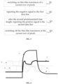
- FIG. 4 is a schematic diagram illustrating a first type of charging of a display panel according to an embodiment of the present application.
- the positive signal is earlier than the negative signal by the first predetermined time length and they are inputted to corresponding data lines to change the phase of the positive signal P and the negative signal N (positive polarity is at the front and negative polarity is at the rear), thereby increasing charging duration of the positive signal P, improving the charging rate, decreasing charging duration of the negative signal N, avoiding mischarge, and thereby improving the whole charging rate of the display panel.
- Step S14 the step of switching off the thin-film transistors of the current row of pixels includes suspending or stopping transmitting a gate signal to the current row of pixels; postponing switching off the thin-film transistor corresponding to the first data line inputted with the positive signal until a first time length is passed; postponing switching off the thin-film transistor corresponding to the second data line inputted with the negative signal until a second time length is passed.
- the second time length is greater than the first time length.
- suspending or stopping transmitting the gate signal to the current row of pixels means disabling the gate signal of the current row of scan line. Since the falling edge of the gate signal occupies a long time, the voltage of the positive signal is high and the voltage of the negative signal is low, the thin-film transistor corresponding to the positive signal will be switched off earlier than the thin-film transistor corresponding to the negative signal even in case of the same gate signal.
- the method further includes obtaining a time difference between the time to switch off the thin-film transistor corresponding to the first data line inputted with the positive signal and the time to switch off the thin-film transistor corresponding to the second data line inputted with the negative signal; the first predetermined time length is the length of the time difference.
- the pixel includes the thin-film transistor and a pixel electrode electrically connected to the thin-film transistor.
- the thin-film transistor is a P-type transistor or a N-type transistor.
- the gate signal of the current row of pixels is switched off such that the thin-film transistors of the current row of pixels are switched off.
- the thin-film transistor is considered to be switched off.
- the thin-film transistor corresponding to the positive polarity will be switched off earlier than the thin-film transistor corresponding to the negative polarity even in case of the same gate signal. Therefore, when the positive and negative signals are inputted to corresponding data lines simultaneously, the charging duration for the positive polarity is shorter than the charging duration for the negative polarity.
- the length of the time difference may be between 0.5 microsecond (including 0.5 microsecond) and 1 microsecond (including 1 microsecond).
- the length of the time difference can be 0.6 microsecond, 0.7 microsecond, 0.8 microsecond or 0.9 microsecond.
- FIG. 5 is a schematic flowchart of a second specific type of pixel charging method according to an embodiment of the present application.
- the step of during the second frame of image, inputting the negative signal to the first data line, and after the second predetermined time length, inputting the positive signal to the second data line includes:
- the display panel may include a display substrate, and a plurality of rows of scan lines, a plurality of columns of data lines, and multiple rows and columns of pixels disposed on the display substrate. It is to be understood that each pixel is electrically connected to one row of scan line and one column of data line, and when a gate signal is inputted to a certain row of scan line to switch on thin-film transistors and a voltage signal is written to a certain column of data line, the voltage signal can charge the pixel connected to the row of scan line and the column of data line.
- the gate of the thin-film transistor of each pixel is electrically connected to one scan line, and the source or the drain of the thin-film transistor of each pixel is electrically connected to one data line.
- the negative signal may be inputted to the first data line based on a result from confirmation on the polarity of the voltage signal that is required to be inputted to either the first data line or the second data line. For example, it is required to input the negative signal to the first data line during an i-th frame of image (where i is a positive integer) based on the confirmation result. Then, when the thin-film transistors of the current row are switched on, the first data line is inputted with the negative signal.
- Step S23 on the basis of the example mentioned in Step S12, the negative signal is to be inputted to the second data signal based on the confirmation result. Then, after the second predetermined time length, the second data line is inputted with the positive signal.
- the second predetermined time length may be between 0.5 microsecond (including 0.5 microsecond) and 1 microsecond (including 1 microsecond). In the present embodiment, the second predetermined time length can be 0.6 microsecond, 0.7 microsecond, 0.8 microsecond or 0.9 microsecond.
- FIG. 6 is a schematic diagram illustrating a second type of charging of a display panel according to an embodiment of the present application.
- the negative signal is earlier than the positive signal by the second predetermined time length and they are inputted to corresponding data lines to change the phase of the positive signal P and the negative signal N (negative polarity is at the front and positive polarity is at the rear), thereby increasing charging duration of the negative signal N, improving the charging rate, decreasing charging duration of the positive signal N, avoiding mischarge, and thereby improving the whole charging rate of the display panel.
- suspending or stopping transmitting the gate signal to the current row of pixels means disabling the gate signal of the current row of scan line. Since the falling edge of the gate signal occupies a long time, the voltage of the positive signal is high and the voltage of the negative signal is low, the thin-film transistor corresponding to the positive signal will be switched off earlier than the thin-film transistor corresponding to the negative signal even in case of the same gate signal.
- the method further includes obtaining a time difference between the time to switch off the thin-film transistor corresponding to the first data line inputted with the negative signal and the time to switch off the thin-film transistor corresponding to the second data line inputted with the positive signal; the second predetermined time length is the length of the time difference.
- the pixel includes the thin-film transistor and a pixel electrode electrically connected to the thin-film transistor.
- the thin-film transistor is a P-type transistor or a N-type transistor.
- the gate signal of the current row of pixels is switched off such that the thin-film transistors of the current row of pixels are switched off.
- the thin-film transistor is considered to be switched off.
- the thin-film transistor corresponding to the positive polarity will be switched off earlier than the thin-film transistor corresponding to the negative polarity even in case of the same gate signal. Therefore, when the positive and negative signals are inputted to corresponding data lines simultaneously, the charging duration for the positive polarity is shorter than the charging duration for the negative polarity.
- the embodiment of the present application is to obtain the length of the time difference.
- the time difference may be an average of or a middle of time differences obtained by switching off the thin-film transistor for many times for the current row, or may be other value.
- the length of the time difference may be between 0.5 microsecond (including 0.5 microsecond) and 1 microsecond (including 1 microsecond).
- the length of the time difference can be 0.6 microsecond, 0.7 microsecond, 0.8 microsecond or 0.9 microsecond.
- the first predetermined time length is equal to the second predetermined time length. That is, in the pixel charging method of the present application, during the first frame of image, the positive signal is inputted to a part of the data lines, and after the first predetermined time length, the negative signal is inputted to the other data lines, and in such a way, the phase of the positive and negative signals is changed (positive polarity is at the front and negative polarity is at the rear); during the second frame of image, the negative signal is inputted to a part of the data lines, and after the second predetermined time length, the positive signal is inputted to the other data lines, and in such a way, the phase of the positive and negative signals is changed (negative polarity is at the front and positive polarity is at the rear).
- the power source voltage will drift based on the polarity and has a first time of power supply interference; during the second frame of image, the power source voltage will drift based on the polarity and has a second time of power supply interference.
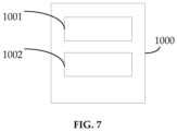
- FIG. 7 is a schematic diagram illustrating the structure of a display panel according to an embodiment of the present application.
- the embodiment of the present application further relates to a display panel 1000, which includes a first charging module 1001 and a second charging module 1002.
- the first charging module 1001 is configured to, during a first frame of image, input a positive signal to the first data line, and after a first predetermined time length, input a negative signal to the second data line.
- the second charging module 1002 is configured to, during a second frame of image, input the negative signal to the first data line, and after a second predetermined time length, input the positive signal to the second data line.
- the display panel of the embodiment of the present application uses the afore-described pixel charging method, which can be referred to above descriptions and is not repeated herein.
- the positive signal is inputted to a part of the data lines, and after the first predetermined time length, the negative signal is inputted to the other data lines, and in such a way, the phase of the positive and negative signals is changed (positive polarity is at the front and negative polarity is at the rear); during the second frame of image, the negative signal is inputted to a part of the data lines, and after the second predetermined time length, the positive signal is inputted to the other data lines, and in such a way, the phase of the positive and negative signals is changed (negative polarity is at the front and positive polarity is at the rear).
- the power source voltage will drift based on the polarity and has a first time of power supply interference; during the second frame of image, the power source voltage will drift based on the polarity and has a second time of power supply interference.
Landscapes
- Engineering & Computer Science (AREA)
- Physics & Mathematics (AREA)
- General Physics & Mathematics (AREA)
- Chemical & Material Sciences (AREA)
- Crystallography & Structural Chemistry (AREA)
- Computer Hardware Design (AREA)
- Theoretical Computer Science (AREA)
- Nonlinear Science (AREA)
- Mathematical Physics (AREA)
- Optics & Photonics (AREA)
- Control Of Indicators Other Than Cathode Ray Tubes (AREA)
- Liquid Crystal Display Device Control (AREA)
Applications Claiming Priority (2)
| Application Number | Priority Date | Filing Date | Title |
|---|---|---|---|
| CN202111290435.0A CN113990237A (zh) | 2021-11-02 | 2021-11-02 | 像素充电方法及显示面板 |
| PCT/CN2021/129858 WO2023077535A1 (zh) | 2021-11-02 | 2021-11-10 | 像素充电方法及显示面板 |
Publications (2)
| Publication Number | Publication Date |
|---|---|
| EP4428844A1 true EP4428844A1 (de) | 2024-09-11 |
| EP4428844A4 EP4428844A4 (de) | 2025-09-03 |
Family
ID=79745875
Family Applications (1)
| Application Number | Title | Priority Date | Filing Date |
|---|---|---|---|
| EP21814664.5A Pending EP4428844A4 (de) | 2021-11-02 | 2021-11-10 | Pixelladeverfahren und anzeigetafel |
Country Status (6)
| Country | Link |
|---|---|
| US (1) | US12073805B2 (de) |
| EP (1) | EP4428844A4 (de) |
| JP (1) | JP7553475B2 (de) |
| KR (1) | KR102836832B1 (de) |
| CN (1) | CN113990237A (de) |
| WO (1) | WO2023077535A1 (de) |
Families Citing this family (1)
| Publication number | Priority date | Publication date | Assignee | Title |
|---|---|---|---|---|
| WO2023168586A1 (zh) * | 2022-03-08 | 2023-09-14 | 京东方科技集团股份有限公司 | 显示面板的驱动方法及显示装置 |
Family Cites Families (16)
| Publication number | Priority date | Publication date | Assignee | Title |
|---|---|---|---|---|
| KR100751172B1 (ko) * | 2000-12-29 | 2007-08-22 | 엘지.필립스 엘시디 주식회사 | 2-도트 인버젼 방식 액정 패널 구동 방법 및 그 장치 |
| JP4400593B2 (ja) | 2006-05-19 | 2010-01-20 | セイコーエプソン株式会社 | 電気光学装置、その駆動方法および電子機器 |
| KR20080089992A (ko) * | 2007-04-03 | 2008-10-08 | 삼성전자주식회사 | 표시 기판 및 이를 포함하는 액정 표시 장치 |
| KR101982716B1 (ko) * | 2012-02-28 | 2019-05-29 | 삼성디스플레이 주식회사 | 표시장치 |
| KR102245640B1 (ko) * | 2014-09-29 | 2021-04-29 | 삼성디스플레이 주식회사 | 데이터 구동 회로 및 이를 포함하는 표시 장치 |
| KR102370280B1 (ko) * | 2014-10-24 | 2022-03-07 | 삼성디스플레이 주식회사 | 적응적 블랙 클리핑 회로, 이를 포함하는 디스플레이 장치 및 적응적 블랙 클리핑 방법 |
| KR102371896B1 (ko) * | 2015-06-29 | 2022-03-11 | 삼성디스플레이 주식회사 | 표시 패널의 구동 방법 및 이를 수행하는 표시 장치 |
| CN105047170B (zh) | 2015-09-09 | 2017-08-25 | 深圳市华星光电技术有限公司 | 驱动装置及液晶显示装置 |
| CN105654917B (zh) | 2016-04-08 | 2018-03-30 | 京东方科技集团股份有限公司 | 极性反转驱动方法、数据驱动器及液晶面板 |
| CN107123408B (zh) | 2017-06-22 | 2019-08-30 | 深圳市华星光电技术有限公司 | 公共电压产生电路及液晶显示器 |
| KR102409823B1 (ko) * | 2017-08-17 | 2022-06-17 | 삼성디스플레이 주식회사 | 표시 패널 구동 회로 및 이를 구비한 표시 장치 |
| CN107507594B (zh) | 2017-09-21 | 2020-06-05 | 深圳市华星光电技术有限公司 | 液晶面板的驱动方法及装置 |
| CN109192168B (zh) * | 2018-10-17 | 2021-08-20 | 维沃移动通信有限公司 | 一种像素充电方法及电子设备 |
| US11189241B2 (en) * | 2020-03-27 | 2021-11-30 | Tcl China Star Optoelectronics Technology Co., Ltd | Method for charging pixels and display panel |
| CN111276109A (zh) * | 2020-03-27 | 2020-06-12 | Tcl华星光电技术有限公司 | 像素充电方法及显示面板 |
| CN111489717A (zh) | 2020-05-12 | 2020-08-04 | Tcl华星光电技术有限公司 | 液晶显示面板及液晶显示面板的充电控制方法 |
-
2021
- 2021-11-02 CN CN202111290435.0A patent/CN113990237A/zh active Pending
- 2021-11-10 EP EP21814664.5A patent/EP4428844A4/de active Pending
- 2021-11-10 US US17/614,734 patent/US12073805B2/en active Active
- 2021-11-10 WO PCT/CN2021/129858 patent/WO2023077535A1/zh not_active Ceased
- 2021-11-10 JP JP2021568782A patent/JP7553475B2/ja active Active
- 2021-11-10 KR KR1020227001228A patent/KR102836832B1/ko active Active
Also Published As
| Publication number | Publication date |
|---|---|
| KR20230066260A (ko) | 2023-05-15 |
| JP2023551609A (ja) | 2023-12-11 |
| CN113990237A (zh) | 2022-01-28 |
| WO2023077535A1 (zh) | 2023-05-11 |
| JP7553475B2 (ja) | 2024-09-18 |
| US12073805B2 (en) | 2024-08-27 |
| KR102836832B1 (ko) | 2025-07-22 |
| EP4428844A4 (de) | 2025-09-03 |
| US20240029680A1 (en) | 2024-01-25 |
Similar Documents
| Publication | Publication Date | Title |
|---|---|---|
| US20150116308A1 (en) | Pixel driving circuit and method, array substrate and liquid crystal display apparatus | |
| US20170148404A1 (en) | Liquid crystal display panel, display device, and driving method | |
| CN101329843B (zh) | 液晶显示装置及其驱动方法 | |
| EP2874002A1 (de) | Arraysubstrat, flüssigkristallanzeigetafel und ansteuerverfahren dafür | |
| US10192510B2 (en) | Source driving module generating two groups of gamma voltages and liquid crystal display device using same | |
| CN106297723B (zh) | 一种像素驱动电路、显示面板以及像素驱动方法 | |
| CN103198804A (zh) | 一种液晶显示装置及其驱动方法 | |
| CN104155820A (zh) | 一种阵列基板及驱动方法 | |
| CN103235431B (zh) | 液晶显示面板及其驱动方法 | |
| US10984745B2 (en) | Driving method and device of display panel, and display device | |
| US20190340988A1 (en) | Display device and method for driving the same | |
| US20210210041A1 (en) | Method for charging liquid crystal pixels, display panel, and storage medium | |
| US11830452B2 (en) | Display panel, display panel driving method, and electronic device | |
| US10074332B2 (en) | Display panel and driving method thereof | |
| CN104464680A (zh) | 一种阵列基板和显示装置 | |
| US10255983B2 (en) | Shift register, unit thereof, and display device | |
| US10446105B2 (en) | Thin film transistor liquid crystal display panel | |
| US9460672B2 (en) | Method for driving a liquid crystal display panel and liquid crystal display | |
| US12073805B2 (en) | Pixel charging method and display panel | |
| US11189241B2 (en) | Method for charging pixels and display panel | |
| CN113628588B (zh) | 显示驱动模组、显示装置及显示方法 | |
| US20150325161A1 (en) | Method and device for controlling voltage of electrode | |
| US11367409B2 (en) | Liquid crystal driving circuit and method solving insufficient charging time of target voltage applied to pixel electrode | |
| US20180053485A1 (en) | Display panel driving method and display panel driving device | |
| CN109147700B (zh) | 阵列基板和显示面板 |
Legal Events
| Date | Code | Title | Description |
|---|---|---|---|
| STAA | Information on the status of an ep patent application or granted ep patent |
Free format text: STATUS: UNKNOWN |
|
| STAA | Information on the status of an ep patent application or granted ep patent |
Free format text: STATUS: THE INTERNATIONAL PUBLICATION HAS BEEN MADE |
|
| PUAI | Public reference made under article 153(3) epc to a published international application that has entered the european phase |
Free format text: ORIGINAL CODE: 0009012 |
|
| STAA | Information on the status of an ep patent application or granted ep patent |
Free format text: STATUS: REQUEST FOR EXAMINATION WAS MADE |
|
| 17P | Request for examination filed |
Effective date: 20211206 |
|
| AK | Designated contracting states |
Kind code of ref document: A1 Designated state(s): AL AT BE BG CH CY CZ DE DK EE ES FI FR GB GR HR HU IE IS IT LI LT LU LV MC MK MT NL NO PL PT RO RS SE SI SK SM TR |
|
| DAV | Request for validation of the european patent (deleted) | ||
| DAX | Request for extension of the european patent (deleted) | ||
| A4 | Supplementary search report drawn up and despatched |
Effective date: 20250731 |
|
| RIC1 | Information provided on ipc code assigned before grant |
Ipc: G09G 3/20 20060101AFI20250725BHEP |