EP4421879A1 - Solar cell and manufacturing method thereof, and photovoltaic module - Google Patents
Solar cell and manufacturing method thereof, and photovoltaic module Download PDFInfo
- Publication number
- EP4421879A1 EP4421879A1 EP23189628.3A EP23189628A EP4421879A1 EP 4421879 A1 EP4421879 A1 EP 4421879A1 EP 23189628 A EP23189628 A EP 23189628A EP 4421879 A1 EP4421879 A1 EP 4421879A1
- Authority
- EP
- European Patent Office
- Prior art keywords
- conductive layer
- layer
- doped
- doped conductive
- solar cell
- Prior art date
- Legal status (The legal status is an assumption and is not a legal conclusion. Google has not performed a legal analysis and makes no representation as to the accuracy of the status listed.)
- Granted
Links
Images


Classifications
-
- H—ELECTRICITY
- H10—SEMICONDUCTOR DEVICES; ELECTRIC SOLID-STATE DEVICES NOT OTHERWISE PROVIDED FOR
- H10F—INORGANIC SEMICONDUCTOR DEVICES SENSITIVE TO INFRARED RADIATION, LIGHT, ELECTROMAGNETIC RADIATION OF SHORTER WAVELENGTH OR CORPUSCULAR RADIATION
- H10F10/00—Individual photovoltaic cells, e.g. solar cells
- H10F10/10—Individual photovoltaic cells, e.g. solar cells having potential barriers
- H10F10/16—Photovoltaic cells having only PN heterojunction potential barriers
- H10F10/164—Photovoltaic cells having only PN heterojunction potential barriers comprising heterojunctions with Group IV materials, e.g. ITO/Si or GaAs/SiGe photovoltaic cells
- H10F10/165—Photovoltaic cells having only PN heterojunction potential barriers comprising heterojunctions with Group IV materials, e.g. ITO/Si or GaAs/SiGe photovoltaic cells the heterojunctions being Group IV-IV heterojunctions, e.g. Si/Ge, SiGe/Si or Si/SiC photovoltaic cells
- H10F10/166—Photovoltaic cells having only PN heterojunction potential barriers comprising heterojunctions with Group IV materials, e.g. ITO/Si or GaAs/SiGe photovoltaic cells the heterojunctions being Group IV-IV heterojunctions, e.g. Si/Ge, SiGe/Si or Si/SiC photovoltaic cells the Group IV-IV heterojunctions being heterojunctions of crystalline and amorphous materials, e.g. silicon heterojunction [SHJ] photovoltaic cells
-
- H—ELECTRICITY
- H10—SEMICONDUCTOR DEVICES; ELECTRIC SOLID-STATE DEVICES NOT OTHERWISE PROVIDED FOR
- H10F—INORGANIC SEMICONDUCTOR DEVICES SENSITIVE TO INFRARED RADIATION, LIGHT, ELECTROMAGNETIC RADIATION OF SHORTER WAVELENGTH OR CORPUSCULAR RADIATION
- H10F77/00—Constructional details of devices covered by this subclass
- H10F77/30—Coatings
- H10F77/306—Coatings for devices having potential barriers
- H10F77/311—Coatings for devices having potential barriers for photovoltaic cells
-
- H—ELECTRICITY
- H10—SEMICONDUCTOR DEVICES; ELECTRIC SOLID-STATE DEVICES NOT OTHERWISE PROVIDED FOR
- H10F—INORGANIC SEMICONDUCTOR DEVICES SENSITIVE TO INFRARED RADIATION, LIGHT, ELECTROMAGNETIC RADIATION OF SHORTER WAVELENGTH OR CORPUSCULAR RADIATION
- H10F77/00—Constructional details of devices covered by this subclass
- H10F77/10—Semiconductor bodies
- H10F77/12—Active materials
- H10F77/122—Active materials comprising only Group IV materials
- H10F77/1223—Active materials comprising only Group IV materials characterised by the dopants
-
- H—ELECTRICITY
- H10—SEMICONDUCTOR DEVICES; ELECTRIC SOLID-STATE DEVICES NOT OTHERWISE PROVIDED FOR
- H10F—INORGANIC SEMICONDUCTOR DEVICES SENSITIVE TO INFRARED RADIATION, LIGHT, ELECTROMAGNETIC RADIATION OF SHORTER WAVELENGTH OR CORPUSCULAR RADIATION
- H10F19/00—Integrated devices, or assemblies of multiple devices, comprising at least one photovoltaic cell covered by group H10F10/00, e.g. photovoltaic modules
- H10F19/90—Structures for connecting between photovoltaic cells, e.g. interconnections or insulating spacers
- H10F19/902—Structures for connecting between photovoltaic cells, e.g. interconnections or insulating spacers for series or parallel connection of photovoltaic cells
- H10F19/906—Structures for connecting between photovoltaic cells, e.g. interconnections or insulating spacers for series or parallel connection of photovoltaic cells characterised by the materials of the structures
-
- H—ELECTRICITY
- H10—SEMICONDUCTOR DEVICES; ELECTRIC SOLID-STATE DEVICES NOT OTHERWISE PROVIDED FOR
- H10F—INORGANIC SEMICONDUCTOR DEVICES SENSITIVE TO INFRARED RADIATION, LIGHT, ELECTROMAGNETIC RADIATION OF SHORTER WAVELENGTH OR CORPUSCULAR RADIATION
- H10F10/00—Individual photovoltaic cells, e.g. solar cells
- H10F10/10—Individual photovoltaic cells, e.g. solar cells having potential barriers
- H10F10/14—Photovoltaic cells having only PN homojunction potential barriers
-
- H—ELECTRICITY
- H10—SEMICONDUCTOR DEVICES; ELECTRIC SOLID-STATE DEVICES NOT OTHERWISE PROVIDED FOR
- H10F—INORGANIC SEMICONDUCTOR DEVICES SENSITIVE TO INFRARED RADIATION, LIGHT, ELECTROMAGNETIC RADIATION OF SHORTER WAVELENGTH OR CORPUSCULAR RADIATION
- H10F19/00—Integrated devices, or assemblies of multiple devices, comprising at least one photovoltaic cell covered by group H10F10/00, e.g. photovoltaic modules
-
- H—ELECTRICITY
- H10—SEMICONDUCTOR DEVICES; ELECTRIC SOLID-STATE DEVICES NOT OTHERWISE PROVIDED FOR
- H10F—INORGANIC SEMICONDUCTOR DEVICES SENSITIVE TO INFRARED RADIATION, LIGHT, ELECTROMAGNETIC RADIATION OF SHORTER WAVELENGTH OR CORPUSCULAR RADIATION
- H10F19/00—Integrated devices, or assemblies of multiple devices, comprising at least one photovoltaic cell covered by group H10F10/00, e.g. photovoltaic modules
- H10F19/80—Encapsulations or containers for integrated devices, or assemblies of multiple devices, having photovoltaic cells
-
- H—ELECTRICITY
- H10—SEMICONDUCTOR DEVICES; ELECTRIC SOLID-STATE DEVICES NOT OTHERWISE PROVIDED FOR
- H10F—INORGANIC SEMICONDUCTOR DEVICES SENSITIVE TO INFRARED RADIATION, LIGHT, ELECTROMAGNETIC RADIATION OF SHORTER WAVELENGTH OR CORPUSCULAR RADIATION
- H10F71/00—Manufacture or treatment of devices covered by this subclass
-
- H—ELECTRICITY
- H10—SEMICONDUCTOR DEVICES; ELECTRIC SOLID-STATE DEVICES NOT OTHERWISE PROVIDED FOR
- H10F—INORGANIC SEMICONDUCTOR DEVICES SENSITIVE TO INFRARED RADIATION, LIGHT, ELECTROMAGNETIC RADIATION OF SHORTER WAVELENGTH OR CORPUSCULAR RADIATION
- H10F71/00—Manufacture or treatment of devices covered by this subclass
- H10F71/121—The active layers comprising only Group IV materials
-
- H—ELECTRICITY
- H10—SEMICONDUCTOR DEVICES; ELECTRIC SOLID-STATE DEVICES NOT OTHERWISE PROVIDED FOR
- H10F—INORGANIC SEMICONDUCTOR DEVICES SENSITIVE TO INFRARED RADIATION, LIGHT, ELECTROMAGNETIC RADIATION OF SHORTER WAVELENGTH OR CORPUSCULAR RADIATION
- H10F71/00—Manufacture or treatment of devices covered by this subclass
- H10F71/129—Passivating
-
- H—ELECTRICITY
- H10—SEMICONDUCTOR DEVICES; ELECTRIC SOLID-STATE DEVICES NOT OTHERWISE PROVIDED FOR
- H10F—INORGANIC SEMICONDUCTOR DEVICES SENSITIVE TO INFRARED RADIATION, LIGHT, ELECTROMAGNETIC RADIATION OF SHORTER WAVELENGTH OR CORPUSCULAR RADIATION
- H10F77/00—Constructional details of devices covered by this subclass
- H10F77/10—Semiconductor bodies
- H10F77/12—Active materials
- H10F77/122—Active materials comprising only Group IV materials
- H10F77/1226—Active materials comprising only Group IV materials comprising multiple Group IV elements, e.g. SiC
- H10F77/1227—Active materials comprising only Group IV materials comprising multiple Group IV elements, e.g. SiC characterised by the dopants
-
- H—ELECTRICITY
- H10—SEMICONDUCTOR DEVICES; ELECTRIC SOLID-STATE DEVICES NOT OTHERWISE PROVIDED FOR
- H10F—INORGANIC SEMICONDUCTOR DEVICES SENSITIVE TO INFRARED RADIATION, LIGHT, ELECTROMAGNETIC RADIATION OF SHORTER WAVELENGTH OR CORPUSCULAR RADIATION
- H10F77/00—Constructional details of devices covered by this subclass
- H10F77/10—Semiconductor bodies
- H10F77/14—Shape of semiconductor bodies; Shapes, relative sizes or dispositions of semiconductor regions within semiconductor bodies
- H10F77/143—Shape of semiconductor bodies; Shapes, relative sizes or dispositions of semiconductor regions within semiconductor bodies comprising quantum structures
-
- H—ELECTRICITY
- H10—SEMICONDUCTOR DEVICES; ELECTRIC SOLID-STATE DEVICES NOT OTHERWISE PROVIDED FOR
- H10F—INORGANIC SEMICONDUCTOR DEVICES SENSITIVE TO INFRARED RADIATION, LIGHT, ELECTROMAGNETIC RADIATION OF SHORTER WAVELENGTH OR CORPUSCULAR RADIATION
- H10F77/00—Constructional details of devices covered by this subclass
- H10F77/20—Electrodes
- H10F77/206—Electrodes for devices having potential barriers
- H10F77/211—Electrodes for devices having potential barriers for photovoltaic cells
-
- Y—GENERAL TAGGING OF NEW TECHNOLOGICAL DEVELOPMENTS; GENERAL TAGGING OF CROSS-SECTIONAL TECHNOLOGIES SPANNING OVER SEVERAL SECTIONS OF THE IPC; TECHNICAL SUBJECTS COVERED BY FORMER USPC CROSS-REFERENCE ART COLLECTIONS [XRACs] AND DIGESTS
- Y02—TECHNOLOGIES OR APPLICATIONS FOR MITIGATION OR ADAPTATION AGAINST CLIMATE CHANGE
- Y02P—CLIMATE CHANGE MITIGATION TECHNOLOGIES IN THE PRODUCTION OR PROCESSING OF GOODS
- Y02P70/00—Climate change mitigation technologies in the production process for final industrial or consumer products
- Y02P70/50—Manufacturing or production processes characterised by the final manufactured product
Definitions
- the present disclosure relates to the technical field of photovoltaic cells and, in particular, to a solar cell and a manufacturing method thereof, and a photovoltaic module.
- one or more embodiments of the present disclosure provide a solar cell, the solar cell includes: a semiconductor substrate, the semiconductor substrate including a first surface and a second surface arranged opposite to each other; an emitter and a first passivation layer formed over the first surface of the semiconductor substrate; a tunneling layer formed over the second surface of the semiconductor substrate; a first doped conductive layer and a retardation layer formed on a surface of the tunneling layer, the first doped conductive layer is located between the tunneling layer and the retardation layer, and the first doped conductive layer and the retardation layer correspond to a metallization region; a second doped conductive layer formed over the surface of the tunneling layer, the second doped conductive layer covering the tunneling layer in a non-metallization region and the retardation layer, the retardation layer is configured to retard migration of a doped element in the second doped conductive layer to the first doped conductive layer; a second passivation layer formed over a surface of the second doped conductive layer; and a second
- one or more embodiments of the present disclosure provide a method for manufacturing solar cell, including: providing a semiconductor substrate, the semiconductor substrate including a first surface and a second surface arranged opposite to each other; forming an emitter on the first surface of the semiconductor substrate after texturing; forming a tunneling layer over the second surface of the semiconductor substrate; forming a first non-conductive layer on a surface of the tunneling layer, the first non-conductive layer corresponding to a metallization region and a non-metallization region; forming a retardation layer over a surface of the first non-conductive layer, the retardation layer corresponding to the metallization region; forming a second non-conductive layer over surfaces of the first non-conductive layer and the retardation layer, and doping the second non-conductive layer so that the second non-conductive layer and the first non-conductive layer that is located in the non-metallization region are transformed into a second doped conductive layer, and the first non-conductive layer located in the metallization region is transformed into a first doped conductive layer
- one or more embodiments of the present disclosure provide a photovoltaic module, the photovoltaic module includes a cover plate, a packaging material layer, and at least one solar cell string including a plurality of solar cells according to the first aspect or manufactured with the manufacturing method according to the second aspect.
- Optimizing surface passivation of crystalline silicon solar cell is one of the important manners to improve the efficiency.
- a TOPCon structure is widely favored due to higher theoretical efficiency thereof.
- the TOPCon structure includes ultra-thin silicon oxide and a heavily doped silicon film, which performs good field passivation effect, so that efficiency of a crystalline silicon solar cell manufactured using TOPCon technology has reached more than 26%.
- a-Si:H amorphous silicon
- CVD chemical vapor deposition
- qVD a quasi-Fermi level difference
- Doping concentration of a conventional doped polysilicon layer is required to reach a certain height, so as to form good contact with a metal electrode.
- a polysilicon layer with high doping concentration may have two problems: phosphorus diffusion to an oxide layer may adversely affect the passivation effect of a tunneling layer; and qVD between doped polysilicon and the silicon substrate is small, resulting in a low upper limit of a theoretical open-circuit voltage, thereby limiting improvement of conversion efficiency of the TOPCon solar cell.
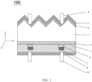
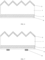
- FIG. 1 shows a schematic structural diagram of a solar cell according to some embodiments of the present disclosure
- the solar cell includes: a semiconductor substrate 1, an emitter 2, a first passivation layer 3, a tunneling layer 4, a first doped conductive layer 5, a retardation layer 6, a second doped conductive layer 7, a second passivation layer 8, a first electrode 9, and a second electrode 10.
- the semiconductor substrate 1 has a first surface and a second surface arranged opposite to each other.
- the emitter 2 and the first passivation layer 3 are located on the first surface of the semiconductor substrate 1.
- the tunneling layer 4 is located on the second surface of the semiconductor substrate 1.
- the first doped conductive layer 5 and the retardation layer 6 are located on a surface of the tunneling layer 4, the first doped conductive layer 5 is located between the tunneling layer 4 and the retardation layer 6, and the first doped conductive layer 5 and the retardation layer 6 correspond to a metallization region.
- the second doped conductive layer 7 is located on the surface of the tunneling layer 4, the second doped conductive layer 7 covers the tunneling layer 4 in a non-metallization region and the retardation layer 6, and a doping concentration of the second doped conductive layer 7 is greater than a doping concentration of the first doped conductive layer 5.
- the second passivation layer 8 is located on a surface of the second doped conductive layer 7.
- the first electrode 9 is in contact with the emitter 2 and a second electrode 10 is in contact with the second doped conductive layer 7.
- the first doped conductive layer 5 with low concentration and the retardation layer 6 are arranged only in the metallization region of the second surface of the solar cell, while the second doped conductive layer 7 with higher concentration is arranged on the entire second surface of the solar cell.
- the first doped conductive layer 5 with lower concentration is in contact with the tunneling layer 4, which can reduce the passivation effect of the doped element on the tunneling layer 4 and reduce recombination current density J 0,metal in the metallization region, and at the same time, a quasi-Fermi level difference qVD between the first doped conductive layer 5 with lower concentration and the semiconductor substrate 1 is smaller, which is conducive to increasing the theoretical open-circuit voltage and thus improving photoelectric conversion efficiency of the solar cell.
- the second doped conductive layer 7 with higher concentration exists in the metallization region and the non-metallization region, which can ensure lateral transport rates of carriers on a rear surface of the solar cell.
- the distance between the second doped conductive layer 7 in the non-metallization region and the semiconductor substrate 1 is relatively short, which can prevent excessive weakening of an energy band bending effect of the second doped conductive layer 7 caused by an excessive long distance between the second doped conductive layer 7 and the semiconductor substrate 1 due to the arrangement of the first doped conductive layer 5 with low concentration and the retardation layer 6, thereby ensuring selective transport of the carriers.
- the design of localized doped conductive layers in the present disclosure can improve the passivation effect in the metallization region, and also ensure lateral transport efficiency of the carriers, which can effectively improve efficiency of the solar cell.
- the first surface of the semiconductor substrate 1 may be a front surface of the solar cell or the rear surface of the solar cell.
- the second surface of the semiconductor substrate 1 is the rear surface of the solar cell.
- the first surface of the semiconductor substrate 1 is the rear surface of the solar cell
- the second surface of the semiconductor substrate 1 is the front surface of the solar cell.
- the front surface of the solar cell is a surface facing the sun (i.e., a light-receiving surface)
- the rear surface of the solar cell is a surface facing away from the sun (i.e., a backlight surface). The following descriptions are all based on examples in which the first surface of the semiconductor substrate 1 is the front surface of the solar cell and the second surface of the semiconductor substrate 1 is the rear surface of the solar cell.
- the metallization region refers to a region where the second electrode 10 of the solar cell penetrates through the second passivation layer 8 to form (direct or indirect) contact with the doped conductive layer.
- conductive metal particles during electrode formation may dissociate from the main structure of the electrode to form indirect contact.
- the non-metallization region refers to regions other than the region where the second electrode 10 penetrates through the second passivation layer 8 and forms contact with the doped conductive layer or a region other than the metallization region.
- the semiconductor substrate 1 is an N-type crystalline silicon substrate (or silicon wafer), or a P-type crystalline silicon substrate (silicon wafer).
- the crystalline silicon substrate (silicon substrate) is, for example, one of a polycrystalline silicon substrate, a monocrystalline silicon substrate, a microcrystalline silicon substrate, or a silicon carbide substrate.
- a specific type of the semiconductor substrate 1 is not limited in the embodiments of the present disclosure.
- a doped element of the semiconductor substrate 1 may be phosphorus, nitrogen, or the like.
- a thickness of the semiconductor substrate 1 ranges from 60 ⁇ m to 240 ⁇ m, which may be, for example, 60 ⁇ m, 80 ⁇ m, 90 ⁇ m, 100 ⁇ m, 120 ⁇ m, 150 ⁇ m, 200 ⁇ m, 240 ⁇ m, or the like, which is not limited herein.
- the emitter 2 may have an emitter 2 structure with a uniform doping depth, or have a selective emitter 2 structure with a different doping concentration and a different doping depth.
- the selective emitter 2 is a heavily doped emitter region corresponding to the metal electrode, and other regions are lightly doped emitter regions.
- the emitter 2 region may be located within the surface of the semiconductor substrate 1, or located outside the surface of the semiconductor substrate 1 to form an independent emitter 2 structure.
- the semiconductor substrate 1 is N-type
- the emitter 2 is P-type, and the semiconductor substrate 1 and the emitter 2 form a PN junction.
- the first passivation layer 3 may include, but is not limited to, a single-layer oxide layer or a multi-layer structure such as silicon oxide, silicon nitride, silicon oxynitride, or aluminum oxide.
- the first passivation layer 3 can produce good passivation effect on the semiconductor substrate 1 and help to improve conversion efficiency of the solar cell. It is to be noted that the first passivation layer 3 may also play a role in reducing reflection of incident light, which, in some examples, may be called as an anti-reflection layer.
- a thickness of the first passivation layer 3 ranges from 10 nm to 120 nm, which may be, for example, 10 nm, 20 nm, 30 nm, 42 nm, 50 nm, 60 nm, 70 nm, 80 nm, 90 nm, 100 nm, 120 nm, or the like, and may be other values in the above range, which is not limited herein.
- the tunneling layer 4 is a thin oxide layer, which may be, for example, silicon oxide or metal oxide, and may include other additional elements, such as nitrogen.
- the tunneling layer 4 may be a stacked structure of one or more of a silicon oxide layer, an aluminum oxide layer, a silicon oxynitride layer, a molybdenum oxide layer, or a hafnium oxide layer.
- the tunneling layer 4 may be an oxygen-containing silicon nitride layer, an oxygen-containing silicon carbide layer, or the like.
- the tunneling layer 4 may not have perfect tunneling barrier in practice, due to, for example, defects such as pinholes, which may lead to dominance of other charge carrier transport mechanisms (e.g., drift and diffusion) over the tunneling effect.
- a thickness of the tunneling layer 4 ranges from 0.5 nm to 2 nm, which may be, for example, 0.5 nm, 0.8 nm, 1 nm, 1.2 nm, 1.5 nm, 1.8 nm, 2 nm, or the like.
- the thinner tunneling layer 4 in the present disclosure helps to prevent transport of majority carriers and promote tunneling collection of minority carriers.
- the first doped conductive layer 5 includes semiconductor materials such as polysilicon, microcrystalline silicon, and silicon carbide.
- a specific type of the first doped conductive layer 5 is not limited in the embodiments of the present disclosure.
- the material of the first doped conductive layer 5 includes polysilicon. That is, the first doped conductive layer 5 is a first doped polysilicon layer, and the second doped conductive layer 7 is a second doped polysilicon layer.
- a doped element in the first doped conductive layer 5 includes at least one of boron, phosphorus, gallium, or arsenic.
- the doping concentration of the first doped conductive layer 5 ranges from 1E18 cm -3 to 1.5E21 cm -3 , which may be, for example, 1E18 cm -3 , 3E18 cm -3 , 8E18 cm -3 , 1E19 cm -3 , 5E19 cm -3 , 1E20 cm -3 , 5E20 cm -3 , 8E20 cm -3 , 1E21 cm -3 , 1.5E21 cm -3 , or the like.
- the first doped conductive layer 5 is a phosphorus-doped polysilicon layer.
- Concentration of phosphorus in the phosphorus-doped polysilicon layer ranges from 1E19 cm -3 to 1.5E21 cm -3 , which may be, for example, 1E19 cm -3 , 5E19 cm -3 , 1E20 cm -3 , 5E20 cm -3 , 8E20 cm -3 , 1E21 cm -3 , 1.5E21 cm -3 , or the like.
- the concentration of the phosphorus in the phosphorus-doped polysilicon layer is controlled within the above range, it is conducive to obtaining excellent passivation and metal contact performance. It may be understood that the concentration of the phosphorus in the phosphorus-doped polysilicon layer refers to concentration of the doped element phosphorus in the phosphorus-doped polysilicon layer that only occupies positions of silicon lattices.
- the first doped conductive layer 5 is an arsenic-doped polysilicon layer.
- Concentration of arsenic in the arsenic-doped polysilicon layer ranges from 1E19 cm -3 to 1.5E21 cm -3 , which may be, for example, 1E19 cm -3 , 5E19 cm -3 , 1E20 cm -3 , 5E20 cm -3 , 8E20 cm -3 , 1E21 cm -3 , 1.5E21 cm -3 , or the like.
- concentration of the arsenic in the arsenic-doped polysilicon layer is controlled within the above range, it is conducive to obtaining excellent passivation and metal contact performance.
- the first doped conductive layer 5 is a boron-doped polysilicon layer.
- Concentration of boron in the boron-doped polysilicon layer ranges from 1E18 cm -3 to 4.5E19 cm -3 , which may be, for example, 1E18 cm -3 , 5E18 cm -3 , 1E19 cm -3 , 2E19 cm -3 , 3E19 cm -3 , 4E19 cm -3 , 4.5E19 cm -3 , or the like.
- concentration of the boron in the boron-doped polysilicon layer is controlled within the above range, it is conducive to obtaining excellent passivation performance, and contact with the metal electrode is ensured at the same time.
- the first doped conductive layer 5 is a gallium-doped polysilicon layer.
- Concentration of gallium in the gallium-doped polysilicon layer ranges from 1E18 cm -3 to 4.5E19 cm -3 , which may be, for example, 1E18 cm -3 , 5E18 cm -3 , 1E19 cm -3 , 2E19 cm -3 , 3E19 cm -3 , 4E19 cm -3 , 4.5E19 cm -3 , or the like.
- concentration of the gallium in the gallium-doped polysilicon layer is controlled within the above range, it is conducive to obtaining excellent passivation performance, and contact with the metal electrode is ensured at the same time.
- the thickness of the first doped conductive layer 5 ranges from 20 nm to 150 nm, which may be, for example, 20 nm, 30 nm, 40 nm, 50 nm, 60 nm, 70 nm, 80 nm, 90 nm, 100 nm, 110 nm, 120 nm, 130 nm, 140 nm, 150 nm, or the like.
- the retardation layer 6 in the present disclosure is a film layer structure configured to retard migration of a doped element in the second doped conductive layer 7 to the first doped conductive layer 5 in the metallization region, which can reduce diffusion of the doped element to the tunneling layer 4 in the metallization region, increase doping concentration of the doped element in the second doped conductive layer 7, and then improve the field passivation capability.
- the material of the retardation layer 6 includes at least one of silicon oxide (e.g., SiO x ), silicon carbide (e.g., SiC), silicon nitride (e.g., SiN x ), and magnesium fluoride (e.g., MgF 2 ).
- the diffusion rate of doped ions in the above materials is much lower than the diffusion rate of doped ions in polysilicon.
- the tetrahedral lattice structure of a polysilicon body Si-Si is more suitable for diffusion of impurity atoms than the retardation layer.
- SiC has slow diffusion of impurity elements due to an amorphous state thereof
- SiO x has slow diffusion of impurity elements due to its own lattice characteristics, so that the impurity elements stay in the retardation layer for a long time and slowly diffuse, thereby playing a retarding role.
- the retardation capability of the retardation layer 6 is defined by a longest distance that thermally diffused doped ions can migrate in a direction of the first doped conductive layer towards the tunneling layer. If the longest distance that the doped ions can migrate is shorter, the retardation capability of the retardation layer 6 is stronger. If the longest distance that the doped ions can migrate is longer, the retardation capability of the retardation layer 6 is weaker.
- an orthographic projection of the retardation layer 6 on the tunneling layer 4 overlaps with an orthographic projection of the first doped conductive layer 5 on the tunneling layer 4.
- the orthographic projection of the retardation layer 6 on the tunneling layer 4 overlaps partially with the orthographic projection of the first doped conductive layer 5 on the tunneling layer 4.
- a thickness of the retardation layer 6 ranges from 0.5 nm to 4 nm, which may be, for example, 0.5 nm, 1 nm, 2 nm, 3 nm, 4 nm, or the like. It may be understood that the thickness direction of the retardation layer 6 refers to a direction from the first doped conductive layer 5 to the tunneling layer 4. When the thickness of the retardation layer 6 is controlled within the above range, the doped element in a direction perpendicular to the surface of the tunneling layer 4 can be retarded from entering the first doped conductive layer 5, so that the doping concentration in the first doped conductive layer 5 is lower.
- the thickness of the retardation layer 6 is less than 0.5 nm, the retardation ability of the retardation layer 6 is poor, and the first doped conductive layer 5 with lower concentration cannot be obtained. If the thickness of the retardation layer 6 is greater than 4 nm, the retardation layer 6 may greatly retard transport of the carriers in a Z-axis direction, which cannot guarantee effective transport of the carriers.
- the concentration of the phosphorus in the phosphorus-doped polysilicon layer refers to concentration of the doped element phosphorus in the phosphorus-doped polysilicon layer that only occupies positions of silicon lattices.
- the second doped conductive layer 7 is an arsenic-doped polysilicon layer.
- Concentration of arsenic in the arsenic-doped polysilicon layer ranges from 5E19 cm -3 to 2E21 cm -3 , which may be, for example, 5E19 cm -3 , 1E20 cm -3 , 5E20 cm -3 , 8E20 cm -3 , 1E21 cm -3 , 2E21 cm -3 , or the like.
- concentration of the arsenic in the arsenic-doped polysilicon layer is controlled within the above range, lateral transport of carriers can be ensured, and it is conducive to increasing the fill factor.
- the first doped conductive layer 5 only corresponds to a local metallization region
- the second doped conductive layer 7 covers the first doped conductive layer 5
- the second doped conductive layer 7 corresponds to an entire rear surface of the solar cell (that is, corresponds to the metallization region and the non-metallization region). Therefore, the thickness of the first doped conductive layer 5 is less than the thickness of the second doped conductive layer 7.
- the second doped conductive layer with higher concentration exists in the metallization region and the non-metallization region, which can ensure lateral transport rates of carriers on a rear surface of the solar cell.
- a distance between the second doped conductive layer in the non-metallization region and the semiconductor substrate is relatively short, which can prevent excessive weakening of an energy band bending effect of the second doped conductive layer caused by an excessive long distance between the second doped conductive layer and the semiconductor substrate due to the arrangement of the first doped conductive layer with low concentration and the retardation layer, thereby ensuring selective transport of the carriers.
- One or more embodiments of the present disclosure further provide a method for manufacturing solar cell, which can be used for manufacturing the solar cell provided in the embodiments of the present disclosure.
- a method for manufacturing solar cell which can be used for manufacturing the solar cell provided in the embodiments of the present disclosure.
- a first non-conductive layer 11 covering the tunneling layer 4 is manufactured first
- the retardation layer 6 is then manufactured in the metallization region
- a second non-conductive layer 12 is manufactured on surfaces of the tunneling layer 4 covering the non-metallization region and the retardation layer 6, and finally doping treatment is performed, so that the second non-conductive layer 12 and the first non-conductive layer 11 that is located in the non-metallization region are transformed into the second doped conductive layer 7 and the first non-conductive layer 11 located in the metallization region is transformed into the first doped conductive layer 5.
- the doped element can diffuse more uniformly throughout the non-metallization region, resulting in existence of fewer of the doped element in the first non-conductive layer 11 located in the non-metallization region and the second non-conductive layer 12. That is, the doping concentration of the second doped conductive layer 7 located in the non-metallization region is greater than the doping concentration of the second doped conductive layer 7 located in the metallization region.
- the doped element in the second doped conductive layer 7 may also diffuse into the first doped conductive layer 5 along the direction parallel to the plane layer where the tunneling layer 4 is located, so that the doping concentration of the first doped conductive layer 5 facing the second doped conductive layer 7 is greater than the doping concentration of the first doped conductive layer 5 facing away from the second doped conductive layer 7.
- the method for manufacturing solar cell provided in the embodiments of the present disclosure may be used for manufacturing a TOPCon solar cell.
- the manufacturing processes for the TOPCon solar cell will be clearly and fully described below with reference to the accompanying drawings in the embodiments of the present disclosure, and the described embodiments are merely some of rather than all of the embodiments of the present disclosure.
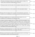
- One or more embodiments of the present disclosure provide a method for manufacturing solar cell. As shown in FIG. 3 , the method includes the following steps.
- a semiconductor substrate 1 is provided, the semiconductor substrate 1 including a first surface and a second surface arranged opposite to each other.
- an emitter 2 is formed on the first surface of the semiconductor substrate 1 after texturing.
- a tunneling layer 4 is formed on the second surface of the semiconductor substrate 1.
- a first non-conductive layer 11 is formed on a surface of the tunneling layer 4, and the first non-conductive layer 11 corresponds to a metallization region and a non-metallization region.
- a retardation layer 6 is formed on a surface of the first non-conductive layer 11, and the retardation layer 6 corresponds to the metallization region.
- a second non-conductive layer 12 is formed on surfaces of the first non-conductive layer 11 and the retardation layer 6, and the second non-conductive layer 12 is doped so that the second non-conductive layer 12 and the first non-conductive layer 11 that is located in the non-metallization region are transformed into a second doped conductive layer 7, and the first non-conductive layer 11 located in the metallization region is transformed into a first doped conductive layer 5, doping concentration of the second doped conductive layer 7 is greater than doping concentration of the first doped conductive layer 5.
- a second passivation layer 8 is formed on a surface of the second doped conductive layer 7 and a first passivation layer 3 is formed on a surface of the emitter 2.
- a second electrode 10 is formed on a surface of the second passivation layer 8 and a first electrode 9 is formed on a surface of the first passivation layer 3.
- the first non-conductive layer 11, the retardation layer 6, and the second non-conductive layer 12 are sequentially formed on the second surface of the semiconductor substrate 1, then doping treatment is performed, and due to the existence of the retardation layer 6, during the doping treatment, fewer of the doped element may enter the first non-conductive layer 11 between the retardation layer 6 and the tunneling layer 4, so that the second non-conductive layer 12 and the first non-conductive layer 11 that is located in the non-metallization region are transformed into the second doped conductive layer 7, and the first non-conductive layer 11 located in the metallization region is transformed into the first doped conductive layer 5, wherein the doping concentration of the second doped conductive layer 7 is greater than the doping concentration of the first doped conductive layer 5.
- the first doped conductive layer 5 with lower concentration is in contact with the tunneling layer 4, which can reduce the passivation effect of the doped element on the tunneling layer 4, and at the same time, a quasi-Fermi level difference qVD between the first doped conductive layer 5 with lower concentration and the semiconductor substrate 1 is smaller, which is conducive to increasing the theoretical open-circuit voltage and improving photoelectric conversion efficiency of the solar cell.
- the second doped conductive layer 7 with higher concentration exists in the metallization region and the non-metallization region, which can ensure lateral transport rates of carriers on the rear surface of the solar cell.
- a distance between the second doped conductive layer 7 in the non-metallization region and the semiconductor substrate 1 is relatively short, which can prevent excessive weakening of an energy band bending effect of the second doped conductive layer 7 caused by an excessive long distance between the second doped conductive layer 7 and the semiconductor substrate 1 due to the arrangement of the first doped conductive layer 5 with low concentration and the retardation layer 6, thereby ensuring selective transport of the carriers.
- the method for manufacturing solar cell is clearly and fully described based on examples in which the first surface of the semiconductor substrate 1 is the front surface of the solar cell and the second surface of the semiconductor substrate 1 is the rear surface of the solar cell.
- a semiconductor substrate 1 is provided, the semiconductor substrate 1 includes a first surface and a second surface arranged opposite to each other.
- the semiconductor substrate 1 is an N-type crystalline silicon substrate (or silicon wafer), or a P-type crystalline silicon substrate (silicon wafer).
- the crystalline silicon substrate (silicon substrate) is, for example, one of a polycrystalline silicon substrate, a monocrystalline silicon substrate, a microcrystalline silicon substrate, or a silicon carbide substrate.
- the specific type of the semiconductor substrate 1 is not limited in the embodiments of the present disclosure.
- a doped element of the semiconductor substrate 1 may be phosphorus, nitrogen, or the like.
- the thickness of the semiconductor substrate 1 ranges from 110 ⁇ m to 250 ⁇ m.
- the thickness of the semiconductor substrate 1 may be 110 ⁇ m, 120 ⁇ m, 140 ⁇ m, 150 ⁇ m, 160 ⁇ m, 170 ⁇ m, 180 ⁇ m, 190 ⁇ m, 200 ⁇ m, 210 ⁇ m, 220 ⁇ m, 230 ⁇ m, 240 ⁇ m, 250 ⁇ m, or the like.
- the thickness of the semiconductor substrate 1 is not limited in the embodiments of the present disclosure.
- an emitter 2 is formed on the first surface of the semiconductor substrate 1 after texturing.
- the front surface of the semiconductor substrate 1 may be textured to form a textured or surface texture structure (e.g., a pyramid structure).
- the texturing may be, for example, chemical etching, laser etching, a mechanical process, or plasma etching, which is not limited herein.
- the front surface of the semiconductor substrate 1 may be textured using a NaOH solution. Due to anisotropy of corrosion of the NaOH solution, a pyramid textured structure may be manufactured.
- the surface of the semiconductor substrate 1 is textured to have a textured structure, which produces a light trapping effect and increases an amount of light absorbed by the solar cell, so as to improve the conversion efficiency of the solar cell.
- a step of cleaning the N-type semiconductor substrate 1 may also be included to remove metal and organic contaminants from the surface.
- the emitter 2 may be formed on the front surface of the semiconductor substrate 1 by any one or more of high-temperature diffusion, paste doping, and ion implantation.
- the emitter 2 is formed by diffusing boron atoms through a boron source.
- boron tribromide may be used as the boron source for diffusion, so that a microcrystalline silicon phase of crystalline silicon is transformed into a polycrystalline silicon phase.
- Due to high concentration of boron on the surface of the semiconductor substrate 1, a layer of borosilicate glass (BSG) may generally be formed. This layer of BSG has a metal impurity absorption effect, which may affect normal operation of the solar cell and is required to be removed later.
- the emitter 2 may have an emitter 2 structure with a uniform doping depth, or have a selective emitter 2 structure with a different doping concentration and a different doping depth.
- a tunneling layer 4 is formed on the second surface of the semiconductor substrate 1.
- the specific process of forming the tunneling layer 4 is not limited in the embodiments of the present disclosure.
- the rear surface of the semiconductor substrate 1 may be oxidized by any one of ozone oxidation, high-temperature thermal oxidation, and nitric acid oxidation.
- the tunneling layer 4 may be one or more of a silicon oxide layer, an aluminum oxide layer, or a silicon oxynitride layer.
- a first non-conductive layer 11 is formed on a surface of the tunneling layer 4, and the first non-conductive layer 11 corresponds to a metallization region and a non-metallization region.
- the first non-conductive layer 11 adopts low temperature deposition.
- an amorphous silicon layer may be manufactured with any one or more methods of chemical vapor deposition (CVD), physical vapor deposition (PVD), and atomic layer deposition (ALD).
- CVD chemical vapor deposition
- PVD physical vapor deposition
- ALD atomic layer deposition
- the manufacturing method for a doped amorphous silicon layer 400 is not limited in the present disclosure.
- the device for deposition may be a CVD device, a PVD device, an ALD device, or the like.
- a temperature of low temperature deposition ranges from 100°C to 300°C.
- the temperature of low temperature deposition may be, for example, 100°C, 110°C, 120°C, 150°C, 170°C, 200°C, 220°C, 250°C, 300°C, or the like.
- the temperature of low temperature deposition is limited in the above range, it is conducive to forming a non-conductive film layer, and local non-conductive materials can be crystallized, thereby improving photoelectric performance of the solar cell.
- a thickness of the first non-conductive layer 11 ranges from 20 nm to 150 nm, which may be, for example, 20 nm, 30 nm, 40 nm, 50 nm, 60 nm, 70 nm, 80 nm, 90 nm, 100 nm, 110 nm, 120 nm, 130 nm, 140 nm, 150 nm, or the like.
- a retardation layer 6 is formed on a surface of the first non-conductive layer 11, and the retardation layer 6 corresponds to the metallization region.
- local laser treatment is performed on the surface of the first non-conductive layer 11 to form the retardation layer 6 corresponding to the metallization region.
- the local laser treatment process of the present disclosure is simple, with high productivity and easy mass production. It is appreciated that, a localized retardation layer 6 may also be formed in other manners, which is not limited in the present disclosure. During the formation of the retardation layer 6, the retardation layer 6 may be completely located in the metallization region, and part of the retardation layer 6 may be located inside the non-metallization region to obtain a stronger retardation effect.
- laser used in laser treatment has a pulse width ranging from 1 ps to 100 ns, which may be, for example, 1 ps, 100 ps, 500 ps, 1 ns, 5 ns, 10 ns, 50 ns, 100 ns, or the like.
- the laser has a wavelength ranging from 250 nm to 532 nm, which may be, for example, 250 nm, 280 nm, 300 nm, 350 nm, 400 nm, 480 nm, 500 nm, 532 nm, or the like.
- power of laser treatment ranges from 20 mJ/cm 2 to 500 mJ/cm 2 , which may be, for example, 20 mJ/cm 2 , 50 mJ/cm 2 , 80 mJ/cm 2 , 100 mJ/cm 2 , 150 mJ/cm 2 , 200 mJ/cm 2 , 300 mJ/cm 2 , 400 mJ/cm 2 , or 500 mJ/cm 2 .
- Silicon nitride absorbed well in a blue-green band may be treated with low-power laser.
- a material with a wide band gap such as silicon oxide is required to be treated with high-power laser.
- a frequency of laser treatment ranges from 100 kHz to 160 kHz, which may be, for example, 100 kHz, 300 kHz, 800 kHz, 1000 kHz, 1300 kHz, or 1600 kHz.
- a number of times of pulse irradiation of laser treatment ranges from 1 to 5 times.
- a second non-conductive layer 12 is formed on surfaces of the first non-conductive layer 11 and the retardation layer 6, to obtain a structure as shown in FIG. 8 , and the second non-conductive layer 12 is doped to obtain a structure as shown in FIG. 9 .
- the doped element diffuses along the Z-axis direction shown in FIG. 1 . That is, in the metallization region, the doped element is transported sequentially from the second non-conductive layer 12 to the retardation layer 6 and then to the first non-conductive layer 11. During the transport, due to the existence of the retardation layer 6, it is more difficult for the doped element to diffuse from the second non-conductive layer 12 to the first non-conductive layer 11. Under the pressure of doping, part of the doped element may still diffuse into the first non-conductive layer 11.
- the second non-conductive layer 12 and the first non-conductive layer 11 that is located in the non-metallization region are transformed into the second doped conductive layer 7, and the first non-conductive layer 11 located in the metallization region is transformed into the first doped conductive layer 5.
- the doping concentration of the second doped conductive layer 7 is greater than the doping concentration of the first doped conductive layer 5. It may be understood that the thickness of the first doped conductive layer 5 is the thickness of the first non-conductive layer 11, and the thickness of the second doped conductive layer 7 is the thickness of the first non-conductive layer 11 plus the thickness of the second non-conductive layer 12.
- resistance of the doped element entering the first non-conductive layer 11 to become the first doped conductive layer 5 becomes greater and greater, so that the doping concentration of the first doped conductive layer 5 decreases sequentially along the direction from the first doped conductive layer 5 to the tunneling layer 4.
- the doped element can diffuse more uniformly throughout the non-metallization region, resulting in existence of fewer of the doped element in the first non-conductive layer 11 located in the non-metallization region and the second non-conductive layer 12. That is, the doping concentration of the second doped conductive layer 7 located in the non-metallization region is greater than the doping concentration of the second doped conductive layer 7 located in the metallization region.
- the doped element in the second doped conductive layer 7 may also diffuse into the first doped conductive layer 5 along the direction parallel to the plane layer where the tunneling layer 4 is located, so that the doping concentration of the first doped conductive layer 5 facing the second doped conductive layer 7 is greater than the doping concentration of the first doped conductive layer 5 facing away from the second doped conductive layer 7.
- the doping treatment adopts high-temperature deposition diffusion, and the specific manufacturing process thereof includes: introducing nitrogen into a high-temperature device for 20 min, exhausting air in a furnace tube, raising temperature of the high-temperature device to 600°C to 1100°C, introducing an inert gas mixed with a dopant source, such as Ar/N 2 , and reacting at a high temperature for 5 min to 50 min; and then introducing oxygen, continuing oxidation reaction at 600°C to 1100°C for 5 min to 60 min, and cooling down the high-temperature device to room temperature after oxidation.
- a dopant source such as Ar/N 2
- a doped element for the doping treatment includes at least one of boron, gallium, phosphorus, and arsenic.
- a dopant source for the doping treatment includes at least one of a boron source, a gallium source, a phosphorus source, and an arsenic source.
- the boron source may be, for example, at least one of BCl 3 , BBr 3 , B 2 H 4 , an organic boron source, and solid silicon containing high-concentration elemental boron
- the gallium source may be, for example, trimethylgallium or solid silicon containing a high-concentration gallium element
- the phosphorus source may be, for example, at least one of POCl 3 , PH 3 , an organic phosphorus source, and solid silicon containing high-concentration elemental phosphorus.
- the arsenic source may be, for example, AsH 3 or solid silicon containing high-concentration elemental arsenic.
- a conductivity type of the doped element is the same as that of the doped element of the semiconductor substrate 1.
- the doped element is an N-type doped element, such as phosphorus or arsenic, and the formed doped layer may be a phosphorus-doped layer or an arsenic-doped silicon layer.
- the semiconductor substrate 1 is a P-type substrate
- the doped element is a P-type doped element, such as boron or gallium
- the formed doped layer is a boron-doped layer or a gallium-doped layer.
- a second passivation layer 8 is formed on a surface of the second doped conductive layer 7 and a first passivation layer 3 is formed on a surface of the emitter 2.
- the first passivation layer 3 may include, but is not limited to, a single-layer oxide layer or a multi-layer structure such as silicon oxide, silicon nitride, silicon oxynitride, or aluminum oxide. It is appreciated that, the first passivation layer 3 may be other types of passivation layers. The specific material of the first passivation layer 3 is not limited in the present disclosure. The above first passivation layer 3 can produce good passivation and anti-reflection effects on the semiconductor substrate 1, which helps to improve the conversion efficiency of the solar cell.
- the second passivation layer 8 may include, but is not limited to, a single-layer oxide layer or a multi-layer structure such as silicon oxide, silicon nitride, silicon oxynitride, or aluminum oxide.
- the second passivation layer 8 is made of silicon nitride.
- a silicon nitride thin-film layer may serve as an anti-reflection film, and the silicon nitride thin film has good insulation, compactness, stability, and a shielding capability for impurity ions.
- the silicon nitride thin-film layer can perform passivation to the semiconductor substrate 1, and obviously improve the photoelectric conversion efficiency of the solar cell.
- a second electrode 10 is formed on a surface of the second passivation layer 8 and a first electrode 9 is formed on a surface of the first passivation layer 3.
- a front busbar and a front finger are printed with paste and dried to form the corresponding front electrode 9.
- a rear busbar and a rear finger may be printed with paste and dried to form the corresponding second electrode 10. Finally, dried solar cells are sintered to manufacture the solar cell.
- the front electrode 9 and the second electrode 10 are not limited in the embodiments of the present disclosure.
- the front electrode 9 is a silver electrode or a silver/aluminum electrode
- the second electrode 10 is a silver electrode or a silver/aluminum electrode.
- one or more embodiments of the present disclosure provide a photovoltaic module 1000, including at least one solar cell string formed by the solar cells described above through electrical connection.
- the photovoltaic module 1000 includes a first cover plate 200, a first packaging adhesive layer 300, at least one solar cell string, a second packaging adhesive layer 400, and a second cover plate 500.
- the solar cell string includes a plurality of solar cells 100 as described above that are connected by conductive strips.
- the solar cells 100 may be connected by partial stacking or by splicing.
- first cover plate 200 and the second cover plate 500 may be transparent or opaque cover plates, such as glass cover plates or plastic cover plates.
- the first packaging adhesive layer 300 and the second packaging adhesive layer 400 each may be an ethylene-vinyl acetate copolymer (EVA) adhesive film, a polyethylene octene co-elastomer (POE) adhesive film or a polyethylene terephthalate (PET) adhesive film.
- EVA ethylene-vinyl acetate copolymer
- POE polyethylene octene co-elastomer
- PET polyethylene terephthalate
- Side edges of the photovoltaic module 1000 may also be completely packaged. That is, the side edges of the photovoltaic module 1000 are fully packaged with a packaging adhesive tape to prevent lamination deviation during the lamination of the photovoltaic module 1000.
- the photovoltaic module 1000 further includes an edge sealing member.
- the edge sealing member is fixedly packaged to a partial edge of the photovoltaic module 1000.
- the edge sealing member may be fixedly packaged to an edge near a corner of the photovoltaic module 1000.
- the edge sealing member may be a high-temperature resistant tape.
- the high-temperature resistant tape has excellent high-temperature resistance and may not decompose or fall off during the lamination, which can ensure the reliable packaging of the photovoltaic module 1000. Two ends of the high-temperature resistant tape are fixed to the second cover plate 500 and the first cover plate 200 respectively.
Landscapes
- Photovoltaic Devices (AREA)
- Engineering & Computer Science (AREA)
- Life Sciences & Earth Sciences (AREA)
- Sustainable Development (AREA)
- Sustainable Energy (AREA)
- Manufacturing & Machinery (AREA)
- Chemical & Material Sciences (AREA)
- Crystallography & Structural Chemistry (AREA)
Abstract
Description
- The present disclosure relates to the technical field of photovoltaic cells and, in particular, to a solar cell and a manufacturing method thereof, and a photovoltaic module.
- With continuous development of the solar cell technologies, the recombination loss in a metal contact region has become one of the most significant constraint factors in improvement of solar cell conversion efficiency. To improve a conversion rate of a solar cell, passivation is generally conducted on the solar cell =by passivated contact, so as to reduce recombinations inside and on surfaces of the solar cell. Common passivated contact solar cells are Heterojunction with Intrinsic Thin-layer (HIT) solar cells and Tunnel Oxide Passivated Contact (TOPCon) solar cells. However, there is limited improvement in passivation performance of the passivation structure of the existing solar cell, so that conversion efficiency of the passivated contact solar cell needs to be improved, and thus difficult in mass production.
- Therefore, how to improve the passivation performance of the passivated contact solar cell has become an urgent problem to be solved in the photovoltaic industry.
- In view of the above, the present disclosure proposes a solar cell, a method for solar cell, and a photovoltaic module. The solar cell can ensure lateral transport capabilities of carriers while improving low passivation performance of a metallization region.
- In a first aspect, one or more embodiments of the present disclosure provide a solar cell, the solar cell includes: a semiconductor substrate, the semiconductor substrate including a first surface and a second surface arranged opposite to each other; an emitter and a first passivation layer formed over the first surface of the semiconductor substrate; a tunneling layer formed over the second surface of the semiconductor substrate; a first doped conductive layer and a retardation layer formed on a surface of the tunneling layer, the first doped conductive layer is located between the tunneling layer and the retardation layer, and the first doped conductive layer and the retardation layer correspond to a metallization region; a second doped conductive layer formed over the surface of the tunneling layer, the second doped conductive layer covering the tunneling layer in a non-metallization region and the retardation layer, the retardation layer is configured to retard migration of a doped element in the second doped conductive layer to the first doped conductive layer; a second passivation layer formed over a surface of the second doped conductive layer; and a second electrode penetrating through the second passivation layer to form contact with the second doped conductive layer and a first electrode penetrating through the first passivation layer to form contact with the emitter.
- In a second aspect, one or more embodiments of the present disclosure provide a method for manufacturing solar cell, including: providing a semiconductor substrate, the semiconductor substrate including a first surface and a second surface arranged opposite to each other; forming an emitter on the first surface of the semiconductor substrate after texturing; forming a tunneling layer over the second surface of the semiconductor substrate; forming a first non-conductive layer on a surface of the tunneling layer, the first non-conductive layer corresponding to a metallization region and a non-metallization region; forming a retardation layer over a surface of the first non-conductive layer, the retardation layer corresponding to the metallization region; forming a second non-conductive layer over surfaces of the first non-conductive layer and the retardation layer, and doping the second non-conductive layer so that the second non-conductive layer and the first non-conductive layer that is located in the non-metallization region are transformed into a second doped conductive layer, and the first non-conductive layer located in the metallization region is transformed into a first doped conductive layer, a doping concentration of the second doped conductive layer is greater than a doping concentration of the first doped conductive layer; forming a second passivation layer over a surface of the second doped conductive layer and forming a first passivation layer over a surface of the emitter; and forming a second electrode on a surface of the second passivation layer and forming a first electrode on a surface of the first passivation layer.
- In a third aspect, one or more embodiments of the present disclosure provide a photovoltaic module, the photovoltaic module includes a cover plate, a packaging material layer, and at least one solar cell string including a plurality of solar cells according to the first aspect or manufactured with the manufacturing method according to the second aspect.
- In order to better illustrate the technical solutions in embodiments of the present disclosure or the related art, the accompanying drawings to be used in the description of the embodiments or the related art will be introduced below. It is apparent that, the accompanying drawings in the following description are only some embodiments of the present disclosure, and other drawings can be obtained by those of ordinary skill in the art from the provided drawings without creative efforts.
-
FIG. 1 is a schematic structural diagram of a solar cell according to one or more embodiments of the present disclosure; -
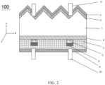
FIG. 2 is a schematic structural diagram of the solar cell according to one or more embodiments of the present disclosure; -
FIG. 3 is a flowchart of manufacturing of the solar cell according to one or more embodiments of the present disclosure; -
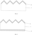
FIG. 4 is a schematic structural diagram of a first emitter formed on a semiconductor substrate according to one or more embodiments of the present disclosure; -
FIG. 5 is a schematic structural diagram of a tunneling layer formed on a second surface of the semiconductor substrate according to one or more embodiments of the present disclosure; -
FIG. 6 is a schematic structural diagram of a first non-conductive layer formed on a surface of the tunneling layer according to one or more embodiments of the present disclosure; -
FIG. 7 is a schematic structural diagram of a retardation layer formed on a surface of the first non-conductive layer according to one or more embodiments of the present disclosure; -
FIG. 8 is a schematic structural diagram of a second non-conductive layer formed on surfaces of the first non-conductive layer and the retardation layer in a non-metallization region according to one or more embodiments of the present disclosure; -
FIG. 9 is a schematic structural diagram after doping treatment of the structure shown inFIG. 8 according to one or more embodiments of the present disclosure; -
FIG. 10 is a schematic structural diagram after a first passivation layer and a second passivation layer are formed on the semiconductor substrate according to one or more embodiments of the present disclosure; and -
FIG. 11 is a schematic structural diagram of a photovoltaic module according to one or more embodiments of the present disclosure. - In order to better understand the technical solutions of the present disclosure, embodiments of the present disclosure will be described in detail below in conjunction with the accompanying drawings.
- It should be clear that the described embodiments are merely some of rather than all of the embodiments of the present disclosure. Based on the embodiments in the present disclosure, all other embodiments obtained by those of ordinary skill in the art without creative efforts fall within the protection scope of the present disclosure.
- The terms used in the embodiments of the present disclosure are intended only to describe particular embodiments and are not intended to limit the present disclosure. As used in the embodiments of the present disclosure and the appended claims, the singular forms of "a/an", "the", and "said" are also intended to include plural forms, unless otherwise clearly indicated in the context.
- It should be understood that the term "and/or" used herein describes an association relationship between associated objects and represents that three relationships may exist. For example, A and/or B may represent the following three cases: only A exists, both A and B exist, and only B exists. In addition, the character "/" herein generally indicates an "or" relationship between the associated objects.
- Optimizing surface passivation of crystalline silicon solar cell is one of the important manners to improve the efficiency. In recent years, with the development of a theoretical technology and people's demand on better passivation effect, a TOPCon structure is widely favored due to higher theoretical efficiency thereof. The TOPCon structure includes ultra-thin silicon oxide and a heavily doped silicon film, which performs good field passivation effect, so that efficiency of a crystalline silicon solar cell manufactured using TOPCon technology has reached more than 26%.
- Most existing TOPCon solar cells use polysilicon (ploy-Si) as a doped layer. A layer of amorphous silicon (a-Si:H) is first deposited by chemical vapor deposition (CVD) and then annealed to transform a-Si: H into poly-Si, which greatly improves the crystallinity, and poly-Si are further doped and activated to improve conductivity of the TOPCon solar cells. Researchers have found that a quasi-Fermi level difference qVD between a silicon substrate and a collection layer is a physical quantity that determines an upper limit of an open-circuit voltage. When qVD is larger, the upper limit of the open-circuit voltage Voc of the solar cell is also higher. Doping concentration of a conventional doped polysilicon layer is required to reach a certain height, so as to form good contact with a metal electrode. However, a polysilicon layer with high doping concentration may have two problems: phosphorus diffusion to an oxide layer may adversely affect the passivation effect of a tunneling layer; and qVD between doped polysilicon and the silicon substrate is small, resulting in a low upper limit of a theoretical open-circuit voltage, thereby limiting improvement of conversion efficiency of the TOPCon solar cell.
- In view of this, embodiments of the present disclosure provide a solar cell.
FIG. 1 shows a schematic structural diagram of a solar cell according to some embodiments of the present disclosure, the solar cell includes: asemiconductor substrate 1, anemitter 2, afirst passivation layer 3, atunneling layer 4, a first dopedconductive layer 5, aretardation layer 6, a second dopedconductive layer 7, asecond passivation layer 8, a first electrode 9, and asecond electrode 10. Thesemiconductor substrate 1 has a first surface and a second surface arranged opposite to each other. Theemitter 2 and thefirst passivation layer 3 are located on the first surface of thesemiconductor substrate 1. Thetunneling layer 4 is located on the second surface of thesemiconductor substrate 1. The first dopedconductive layer 5 and theretardation layer 6 are located on a surface of thetunneling layer 4, the first dopedconductive layer 5 is located between thetunneling layer 4 and theretardation layer 6, and the first dopedconductive layer 5 and theretardation layer 6 correspond to a metallization region. The second dopedconductive layer 7 is located on the surface of thetunneling layer 4, the second dopedconductive layer 7 covers thetunneling layer 4 in a non-metallization region and theretardation layer 6, and a doping concentration of the second dopedconductive layer 7 is greater than a doping concentration of the first dopedconductive layer 5. Thesecond passivation layer 8 is located on a surface of the second dopedconductive layer 7. The first electrode 9 is in contact with theemitter 2 and asecond electrode 10 is in contact with the second dopedconductive layer 7. - The first doped
conductive layer 5 with low concentration and theretardation layer 6 are arranged only in the metallization region of the second surface of the solar cell, while the second dopedconductive layer 7 with higher concentration is arranged on the entire second surface of the solar cell. In this way, on the one hand, the first dopedconductive layer 5 with lower concentration is in contact with thetunneling layer 4, which can reduce the passivation effect of the doped element on thetunneling layer 4 and reduce recombination current density J0,metal in the metallization region, and at the same time, a quasi-Fermi level difference qVD between the first dopedconductive layer 5 with lower concentration and thesemiconductor substrate 1 is smaller, which is conducive to increasing the theoretical open-circuit voltage and thus improving photoelectric conversion efficiency of the solar cell. In addition, the second dopedconductive layer 7 with higher concentration exists in the metallization region and the non-metallization region, which can ensure lateral transport rates of carriers on a rear surface of the solar cell. Moreover, the distance between the second dopedconductive layer 7 in the non-metallization region and thesemiconductor substrate 1 is relatively short, which can prevent excessive weakening of an energy band bending effect of the second dopedconductive layer 7 caused by an excessive long distance between the second dopedconductive layer 7 and thesemiconductor substrate 1 due to the arrangement of the first dopedconductive layer 5 with low concentration and theretardation layer 6, thereby ensuring selective transport of the carriers. Compared with the sequential arrangement of an entire surface of a lightly doped conductive layer, an entire surface of theretardation layer 6, and an entire surface of a heavily doped conductive layer on thetunneling layer 4 on the rear surface of the solar cell to improve the passivation effect, the design of localized doped conductive layers in the present disclosure can improve the passivation effect in the metallization region, and also ensure lateral transport efficiency of the carriers, which can effectively improve efficiency of the solar cell. - In some embodiments, the first surface of the
semiconductor substrate 1 may be a front surface of the solar cell or the rear surface of the solar cell. When the first surface of thesemiconductor substrate 1 is the front surface of the solar cell, the second surface of thesemiconductor substrate 1 is the rear surface of the solar cell. When the first surface of thesemiconductor substrate 1 is the rear surface of the solar cell, the second surface of thesemiconductor substrate 1 is the front surface of the solar cell. It may be understood that the front surface of the solar cell is a surface facing the sun (i.e., a light-receiving surface), and the rear surface of the solar cell is a surface facing away from the sun (i.e., a backlight surface). The following descriptions are all based on examples in which the first surface of thesemiconductor substrate 1 is the front surface of the solar cell and the second surface of thesemiconductor substrate 1 is the rear surface of the solar cell. - For those skilled in the art, the metallization region refers to a region where the
second electrode 10 of the solar cell penetrates through thesecond passivation layer 8 to form (direct or indirect) contact with the doped conductive layer. In some cases, conductive metal particles during electrode formation may dissociate from the main structure of the electrode to form indirect contact. The non-metallization region refers to regions other than the region where thesecond electrode 10 penetrates through thesecond passivation layer 8 and forms contact with the doped conductive layer or a region other than the metallization region. - In some embodiments, the
semiconductor substrate 1 is an N-type crystalline silicon substrate (or silicon wafer), or a P-type crystalline silicon substrate (silicon wafer). The crystalline silicon substrate (silicon substrate) is, for example, one of a polycrystalline silicon substrate, a monocrystalline silicon substrate, a microcrystalline silicon substrate, or a silicon carbide substrate. A specific type of thesemiconductor substrate 1 is not limited in the embodiments of the present disclosure. A doped element of thesemiconductor substrate 1 may be phosphorus, nitrogen, or the like. - In some embodiments, a thickness of the
semiconductor substrate 1 ranges from 60 µm to 240 µm, which may be, for example, 60 µm, 80 µm, 90 µm, 100 µm, 120 µm, 150 µm, 200 µm, 240 µm, or the like, which is not limited herein. - In some embodiments, the
emitter 2 may have anemitter 2 structure with a uniform doping depth, or have aselective emitter 2 structure with a different doping concentration and a different doping depth. For example, theselective emitter 2 is a heavily doped emitter region corresponding to the metal electrode, and other regions are lightly doped emitter regions. Theemitter 2 region may be located within the surface of thesemiconductor substrate 1, or located outside the surface of thesemiconductor substrate 1 to form anindependent emitter 2 structure. When thesemiconductor substrate 1 is N-type, theemitter 2 is P-type, and thesemiconductor substrate 1 and theemitter 2 form a PN junction. - In some embodiments, the
first passivation layer 3 may include, but is not limited to, a single-layer oxide layer or a multi-layer structure such as silicon oxide, silicon nitride, silicon oxynitride, or aluminum oxide. Thefirst passivation layer 3 can produce good passivation effect on thesemiconductor substrate 1 and help to improve conversion efficiency of the solar cell. It is to be noted that thefirst passivation layer 3 may also play a role in reducing reflection of incident light, which, in some examples, may be called as an anti-reflection layer. - In some embodiments, a thickness of the
first passivation layer 3 ranges from 10 nm to 120 nm, which may be, for example, 10 nm, 20 nm, 30 nm, 42 nm, 50 nm, 60 nm, 70 nm, 80 nm, 90 nm, 100 nm, 120 nm, or the like, and may be other values in the above range, which is not limited herein. - In some embodiments, the
tunneling layer 4 is a thin oxide layer, which may be, for example, silicon oxide or metal oxide, and may include other additional elements, such as nitrogen. For example, thetunneling layer 4 may be a stacked structure of one or more of a silicon oxide layer, an aluminum oxide layer, a silicon oxynitride layer, a molybdenum oxide layer, or a hafnium oxide layer. In some other embodiments, thetunneling layer 4 may be an oxygen-containing silicon nitride layer, an oxygen-containing silicon carbide layer, or the like. Thetunneling layer 4 may not have perfect tunneling barrier in practice, due to, for example, defects such as pinholes, which may lead to dominance of other charge carrier transport mechanisms (e.g., drift and diffusion) over the tunneling effect. - In some embodiments, a thickness of the
tunneling layer 4 ranges from 0.5 nm to 2 nm, which may be, for example, 0.5 nm, 0.8 nm, 1 nm, 1.2 nm, 1.5 nm, 1.8 nm, 2 nm, or the like. Thethinner tunneling layer 4 in the present disclosure helps to prevent transport of majority carriers and promote tunneling collection of minority carriers. - In some embodiments, the first doped
conductive layer 5 includes semiconductor materials such as polysilicon, microcrystalline silicon, and silicon carbide. A specific type of the first dopedconductive layer 5 is not limited in the embodiments of the present disclosure. For example, the material of the first dopedconductive layer 5 includes polysilicon. That is, the first dopedconductive layer 5 is a first doped polysilicon layer, and the second dopedconductive layer 7 is a second doped polysilicon layer. - In some embodiments, a doped element in the first doped
conductive layer 5 includes at least one of boron, phosphorus, gallium, or arsenic. - In some embodiments, the doping concentration of the first doped
conductive layer 5 ranges from 1E18 cm-3 to 1.5E21 cm-3, which may be, for example, 1E18 cm-3, 3E18 cm-3, 8E18 cm-3, 1E19 cm-3, 5E19 cm-3, 1E20 cm-3, 5E20 cm-3, 8E20 cm-3, 1E21 cm-3, 1.5E21 cm-3, or the like. - When the doped element in the first doped
conductive layer 5 is phosphorus and the material thereof is polysilicon, the first dopedconductive layer 5 is a phosphorus-doped polysilicon layer. Concentration of phosphorus in the phosphorus-doped polysilicon layer ranges from 1E19 cm-3 to 1.5E21 cm-3, which may be, for example, 1E19 cm-3, 5E19 cm-3, 1E20 cm-3, 5E20 cm-3, 8E20 cm-3, 1E21 cm-3, 1.5E21 cm-3, or the like. When the concentration of the phosphorus in the phosphorus-doped polysilicon layer is controlled within the above range, it is conducive to obtaining excellent passivation and metal contact performance. It may be understood that the concentration of the phosphorus in the phosphorus-doped polysilicon layer refers to concentration of the doped element phosphorus in the phosphorus-doped polysilicon layer that only occupies positions of silicon lattices. - When the doped element in the first doped
conductive layer 5 is arsenic and the material thereof is polysilicon, the first dopedconductive layer 5 is an arsenic-doped polysilicon layer. Concentration of arsenic in the arsenic-doped polysilicon layer ranges from 1E19 cm-3 to 1.5E21 cm-3, which may be, for example, 1E19 cm-3, 5E19 cm-3, 1E20 cm-3, 5E20 cm-3, 8E20 cm-3, 1E21 cm-3, 1.5E21 cm-3, or the like. When the concentration of the arsenic in the arsenic-doped polysilicon layer is controlled within the above range, it is conducive to obtaining excellent passivation and metal contact performance. - When the doped element in the first doped
conductive layer 5 is boron and the material thereof is polysilicon, the first dopedconductive layer 5 is a boron-doped polysilicon layer. Concentration of boron in the boron-doped polysilicon layer ranges from 1E18 cm-3 to 4.5E19 cm-3, which may be, for example, 1E18 cm-3, 5E18 cm-3, 1E19 cm-3, 2E19 cm-3, 3E19 cm-3, 4E19 cm-3, 4.5E19 cm-3, or the like. When the concentration of the boron in the boron-doped polysilicon layer is controlled within the above range, it is conducive to obtaining excellent passivation performance, and contact with the metal electrode is ensured at the same time. - When the doped element in the first doped
conductive layer 5 is gallium and the material thereof is polysilicon, the first dopedconductive layer 5 is a gallium-doped polysilicon layer. Concentration of gallium in the gallium-doped polysilicon layer ranges from 1E18 cm-3 to 4.5E19 cm-3, which may be, for example, 1E18 cm-3, 5E18 cm-3, 1E19 cm-3, 2E19 cm-3, 3E19 cm-3, 4E19 cm-3, 4.5E19 cm-3, or the like. When the concentration of the gallium in the gallium-doped polysilicon layer is controlled within the above range, it is conducive to obtaining excellent passivation performance, and contact with the metal electrode is ensured at the same time. - In some embodiments, the thickness of the first doped
conductive layer 5 ranges from 20 nm to 150 nm, which may be, for example, 20 nm, 30 nm, 40 nm, 50 nm, 60 nm, 70 nm, 80 nm, 90 nm, 100 nm, 110 nm, 120 nm, 130 nm, 140 nm, 150 nm, or the like. - In some embodiments, the
retardation layer 6 in the present disclosure is a film layer structure configured to retard migration of a doped element in the second dopedconductive layer 7 to the first dopedconductive layer 5 in the metallization region, which can reduce diffusion of the doped element to thetunneling layer 4 in the metallization region, increase doping concentration of the doped element in the second dopedconductive layer 7, and then improve the field passivation capability. The material of theretardation layer 6 includes at least one of silicon oxide (e.g., SiOx), silicon carbide (e.g., SiC), silicon nitride (e.g., SiNx), and magnesium fluoride (e.g., MgF2). The diffusion rate of doped ions in the above materials is much lower than the diffusion rate of doped ions in polysilicon. There are many grain boundaries in polysilicon, and the tetrahedral lattice structure of a polysilicon body Si-Si is more suitable for diffusion of impurity atoms than the retardation layer. For example, for the retardation layer, SiC has slow diffusion of impurity elements due to an amorphous state thereof, and SiOx has slow diffusion of impurity elements due to its own lattice characteristics, so that the impurity elements stay in the retardation layer for a long time and slowly diffuse, thereby playing a retarding role. - The retardation capability of the
retardation layer 6 is defined by a longest distance that thermally diffused doped ions can migrate in a direction of the first doped conductive layer towards the tunneling layer. If the longest distance that the doped ions can migrate is shorter, the retardation capability of theretardation layer 6 is stronger. If the longest distance that the doped ions can migrate is longer, the retardation capability of theretardation layer 6 is weaker. - In some embodiments, along a direction parallel to the
tunneling layer 4, that is, along an X-axis direction inFIG. 1 , a ratio of a width of the first dopedconductive layer 5 to a width of theretardation layer 6 is in a range of 1:1 to 1:2, which may be, for example, 1:1, 1:1.2, 1:1.5, 1:1.7, 1:2, or the like. For example, the ratio of the width of the first dopedconductive layer 5 to the width of theretardation layer 6 is 1:1.2.FIG. 2 is a schematic structural diagram of a solar cell in which the ratio of the width of the first dopedconductive layer 5 to the width of theretardation layer 6 is 1:1.2 according to some embodiments of the present disclosure. It may be understood that, in some embodiments, an orthographic projection of theretardation layer 6 on thetunneling layer 4 overlaps with an orthographic projection of the first dopedconductive layer 5 on thetunneling layer 4. In some other embodiments, the orthographic projection of theretardation layer 6 on thetunneling layer 4 overlaps partially with the orthographic projection of the first dopedconductive layer 5 on thetunneling layer 4. Under the limitation of the above ratio, the doping concentration in the first dopedconductive layer 5 can be ensured within a relatively low range, and a passivation effect of the doped element on thetunneling layer 4 can be reduced, which is conducive to increasing the theoretical open-circuit voltage and further improving the conversion efficiency of the solar cell. - In some embodiments, a thickness of the
retardation layer 6 ranges from 0.5 nm to 4 nm, which may be, for example, 0.5 nm, 1 nm, 2 nm, 3 nm, 4 nm, or the like. It may be understood that the thickness direction of theretardation layer 6 refers to a direction from the first dopedconductive layer 5 to thetunneling layer 4. When the thickness of theretardation layer 6 is controlled within the above range, the doped element in a direction perpendicular to the surface of thetunneling layer 4 can be retarded from entering the first dopedconductive layer 5, so that the doping concentration in the first dopedconductive layer 5 is lower. If the thickness of theretardation layer 6 is less than 0.5 nm, the retardation ability of theretardation layer 6 is poor, and the first dopedconductive layer 5 with lower concentration cannot be obtained. If the thickness of theretardation layer 6 is greater than 4 nm, theretardation layer 6 may greatly retard transport of the carriers in a Z-axis direction, which cannot guarantee effective transport of the carriers. - In some embodiments, the second doped
conductive layer 7 covers thetunneling layer 4 in the non-metallization region and theretardation layer 6, and a material of the second dopedconductive layer 7 includes semiconductor materials such as polysilicon, microcrystalline silicon, and silicon carbide. A specific type of the second dopedconductive layer 7 is not limited in the embodiments of the present disclosure. For example, the material of the second dopedconductive layer 7 includes polysilicon. - In some embodiments, a doped element in the second doped
conductive layer 7 includes at least one of boron, phosphorus, gallium, and arsenic. - In some embodiments, the doping concentration of the second doped
conductive layer 7 ranges from 5E18 cm-3 to 2E21 cm-3, which may be, for example, 5E18 cm-3, 8E18 cm-3, 1E19 cm-3, 5E19 cm-3, 1E20 cm-3, 5E20 cm-3, 8E20 cm-3, 1E21 cm-3, 2E21 cm-3, or the like. - When the doped element in the second doped
conductive layer 7 is phosphorus and the material thereof is polysilicon, the second dopedconductive layer 7 is a phosphorus-doped polysilicon layer. Concentration of phosphorus in the phosphorus-doped polysilicon layer ranges from 5E19 cm-3 to 2E21 cm-3, which may be, for example, 5E19 cm-3, 1E20 cm-3, 5E20 cm-3, 8E20 cm-3, 1E21 cm-3, 2E21 cm-3, or the like. When the concentration of the phosphorus in the phosphorus-doped polysilicon layer is controlled within the above range, lateral transport of carriers can be ensured, and it is conducive to increasing the fill factor. It may be understood that the concentration of the phosphorus in the phosphorus-doped polysilicon layer refers to concentration of the doped element phosphorus in the phosphorus-doped polysilicon layer that only occupies positions of silicon lattices. - When the doped element in the second doped
conductive layer 7 is arsenic and the material thereof is polysilicon, the second dopedconductive layer 7 is an arsenic-doped polysilicon layer. Concentration of arsenic in the arsenic-doped polysilicon layer ranges from 5E19 cm-3 to 2E21 cm-3, which may be, for example, 5E19 cm-3, 1E20 cm-3, 5E20 cm-3, 8E20 cm-3, 1E21 cm-3, 2E21 cm-3, or the like. When the concentration of the arsenic in the arsenic-doped polysilicon layer is controlled within the above range, lateral transport of carriers can be ensured, and it is conducive to increasing the fill factor. - When the doped element in the second doped
conductive layer 7 is boron and the material thereof is polysilicon, the second dopedconductive layer 7 is a boron-doped polysilicon layer. Concentration of boron in the boron-doped polysilicon layer ranges from 5E18 cm-3 to 5E19 cm-3, which may be, for example, 5E18 cm-3, 1E19 cm-3, 2E19 cm-3, 3E19 cm-3, 4E19 cm-3, 5E19 cm-3, or the like. When the concentration of the boron in the boron-doped polysilicon layer is controlled within the above range, it is conducive to obtaining excellent passivation performance, and contact with the metal electrode is ensured at the same time. - When the doped element in the second doped
conductive layer 7 is gallium and the material thereof is polysilicon, the second dopedconductive layer 7 is a gallium-doped polysilicon layer. Concentration of gallium in the gallium-doped polysilicon layer ranges from 5E18 cm-3 to 5E19 cm-3, which may be, for example, 5E18 cm-3, 1E19 cm-3, 2E19 cm-3, 3E19 cm-3, 4E19 cm-3, 5E19 cm-3, or the like. When the concentration of the gallium in the gallium-doped polysilicon layer is controlled within the above range, it is conducive to obtaining excellent passivation performance, and contact with the metal electrode is ensured at the same time. - In some embodiments, the thickness of the second doped
conductive layer 7 ranges from 20 nm to 200 nm, which may be, for example, 20 nm, 30 nm, 40 nm, 50 nm, 60 nm, 70 nm, 80 nm, 90 nm, 100 nm, 110 nm, 120 nm, 130 nm, 140 nm, 150 nm, 160 nm, 170 nm, 180 nm, 190 nm, 200 nm, or the like. It may be understood that the first dopedconductive layer 5 only corresponds to a local metallization region, the second dopedconductive layer 7 covers the first dopedconductive layer 5, and the second dopedconductive layer 7 corresponds to an entire rear surface of the solar cell (that is, corresponds to the metallization region and the non-metallization region). Therefore, the thickness of the first dopedconductive layer 5 is less than the thickness of the second dopedconductive layer 7. - In some embodiments, a surface area of the
tunneling layer 4 in contact with the first dopedconductive layer 5 is denoted asS 1, and a sum of the surface area of thetunneling layer 4 in contact with the first dopedconductive layer 5 and a surface area of thetunneling layer 4 in contact with the second dopedconductive layer 7 is denoted as S2, S1:S2 in a range of 1:5 to 1:50, which may be, for example, 1:5, 1:10, 1:20, 1:30, 1:40, 1:45, 1:50, or the like. Within the above range, lateral transport of the carriers of the doped conductive layer in other regions can be ensured while passivation performance of the doped conductive layer in the metallization region can be ensured, which helps to improve the photoelectric conversion efficiency of the solar cell. If S1:S2 is greater than 1:5, the proportion of the first dopedconductive layer 5 is excessively high, resulting in large resistance to the lateral transport of the carriers in the polysilicon layer, an influence on the fill factor of the solar cell, and thus a decrease in the photoelectric conversion efficiency. If S1:S2 is less than 1:50, the proportion of the second dopedconductive layer 7 is excessively high, resulting in an increase in a carrier recombination rate in the metallization region, a significant decrease in the passivation effect, an influence on the open-circuit voltage of the solar cell, and thus a decrease in the photoelectric conversion efficiency. - In the present disclosure, the first doped conductive layer with low concentration and the retardation layer are arranged only in the metallization region of the second surface of the solar cell, while the second doped conductive layer with higher concentration is arranged on the entire second surface of the solar cell, so that, on the one hand, the first doped conductive layer with lower concentration is in contact with the tunneling layer, which can reduce the passivation effect of the doped element on the tunneling layer and reduce recombination current density J0,metal in the metallization region, and at the same time, a quasi-Fermi level difference qVD between the first doped conductive layer with lower concentration and the semiconductor substrate is smaller, which is conducive to increasing the theoretical open-circuit voltage and improving photoelectric conversion efficiency of the solar cell. In addition, the second doped conductive layer with higher concentration exists in the metallization region and the non-metallization region, which can ensure lateral transport rates of carriers on a rear surface of the solar cell. Moreover, a distance between the second doped conductive layer in the non-metallization region and the semiconductor substrate is relatively short, which can prevent excessive weakening of an energy band bending effect of the second doped conductive layer caused by an excessive long distance between the second doped conductive layer and the semiconductor substrate due to the arrangement of the first doped conductive layer with low concentration and the retardation layer, thereby ensuring selective transport of the carriers.
- One or more embodiments of the present disclosure further provide a method for manufacturing solar cell, which can be used for manufacturing the solar cell provided in the embodiments of the present disclosure. During the manufacturing of the doped conductive layer, a first
non-conductive layer 11 covering thetunneling layer 4 is manufactured first, theretardation layer 6 is then manufactured in the metallization region, a secondnon-conductive layer 12 is manufactured on surfaces of thetunneling layer 4 covering the non-metallization region and theretardation layer 6, and finally doping treatment is performed, so that the secondnon-conductive layer 12 and the firstnon-conductive layer 11 that is located in the non-metallization region are transformed into the second dopedconductive layer 7 and the firstnon-conductive layer 11 located in the metallization region is transformed into the first dopedconductive layer 5. Due to the existence of theretardation layer 6, as the doping treatment proceeds, resistance of the doped element entering the firstnon-conductive layer 11 to become the first dopedconductive layer 5 becomes greater and greater, so that the doping concentration of the first dopedconductive layer 5 decreases sequentially along the direction from the first dopedconductive layer 5 to thetunneling layer 4. With the arrangement, the diffusion of the doped element to thetunneling layer 4 can be reduced as much as possible, which is beneficial to improve the passivation performance in the metallization region. - In some embodiments, during the doping treatment, due to the existence of the
retardation layer 6 in the metallization region, transport of the doped element towards the firstnon-conductive layer 11 is prevented, so that more of the doped element exists in the secondnon-conductive layer 12 located in the metallization region. However, in the non-metallization region, without the blocking by theretardation layer 6, the doped element can diffuse more uniformly throughout the non-metallization region, resulting in existence of fewer of the doped element in the firstnon-conductive layer 11 located in the non-metallization region and the secondnon-conductive layer 12. That is, the doping concentration of the second dopedconductive layer 7 located in the non-metallization region is greater than the doping concentration of the second dopedconductive layer 7 located in the metallization region. With the arrangement, concentration of the region in the second dopedconductive layer 7 in contact with thesecond electrode 10 is relatively high, which is conducive to the lateral transport of the carriers and formation of better contact between the second dopedconductive layer 7 and thesecond electrode 10. - In some embodiments, along a direction parallel to a plane layer where the
tunneling layer 4 is located, two sides of the first dopedconductive layer 5 are bordered by the second dopedconductive layer 7 respectively. Therefore, during the doping treatment, the doped element in the second dopedconductive layer 7 may also diffuse into the first dopedconductive layer 5 along the direction parallel to the plane layer where thetunneling layer 4 is located, so that the doping concentration of the first dopedconductive layer 5 facing the second dopedconductive layer 7 is greater than the doping concentration of the first dopedconductive layer 5 facing away from the second dopedconductive layer 7. - The method for manufacturing solar cell provided in the embodiments of the present disclosure may be used for manufacturing a TOPCon solar cell. The manufacturing processes for the TOPCon solar cell will be clearly and fully described below with reference to the accompanying drawings in the embodiments of the present disclosure, and the described embodiments are merely some of rather than all of the embodiments of the present disclosure.
- One or more embodiments of the present disclosure provide a method for manufacturing solar cell. As shown in
FIG. 3 , the method includes the following steps. - In 5100, a
semiconductor substrate 1 is provided, thesemiconductor substrate 1 including a first surface and a second surface arranged opposite to each other. - In S200, an
emitter 2 is formed on the first surface of thesemiconductor substrate 1 after texturing. - In S300, a
tunneling layer 4 is formed on the second surface of thesemiconductor substrate 1. - In S400, a first
non-conductive layer 11 is formed on a surface of thetunneling layer 4, and the firstnon-conductive layer 11 corresponds to a metallization region and a non-metallization region. - In S500, a
retardation layer 6 is formed on a surface of the firstnon-conductive layer 11, and theretardation layer 6 corresponds to the metallization region. - In S600, a second
non-conductive layer 12 is formed on surfaces of the firstnon-conductive layer 11 and theretardation layer 6, and the secondnon-conductive layer 12 is doped so that the secondnon-conductive layer 12 and the firstnon-conductive layer 11 that is located in the non-metallization region are transformed into a second dopedconductive layer 7, and the firstnon-conductive layer 11 located in the metallization region is transformed into a first dopedconductive layer 5, doping concentration of the second dopedconductive layer 7 is greater than doping concentration of the first dopedconductive layer 5. - In S700, a
second passivation layer 8 is formed on a surface of the second dopedconductive layer 7 and afirst passivation layer 3 is formed on a surface of theemitter 2. - In S800, a
second electrode 10 is formed on a surface of thesecond passivation layer 8 and a first electrode 9 is formed on a surface of thefirst passivation layer 3. - In the present disclosure, the first
non-conductive layer 11, theretardation layer 6, and the secondnon-conductive layer 12 are sequentially formed on the second surface of thesemiconductor substrate 1, then doping treatment is performed, and due to the existence of theretardation layer 6, during the doping treatment, fewer of the doped element may enter the firstnon-conductive layer 11 between theretardation layer 6 and thetunneling layer 4, so that the secondnon-conductive layer 12 and the firstnon-conductive layer 11 that is located in the non-metallization region are transformed into the second dopedconductive layer 7, and the firstnon-conductive layer 11 located in the metallization region is transformed into the first dopedconductive layer 5, wherein the doping concentration of the second dopedconductive layer 7 is greater than the doping concentration of the first dopedconductive layer 5. On the one hand, the first dopedconductive layer 5 with lower concentration is in contact with thetunneling layer 4, which can reduce the passivation effect of the doped element on thetunneling layer 4, and at the same time, a quasi-Fermi level difference qVD between the first dopedconductive layer 5 with lower concentration and thesemiconductor substrate 1 is smaller, which is conducive to increasing the theoretical open-circuit voltage and improving photoelectric conversion efficiency of the solar cell. In addition, the second dopedconductive layer 7 with higher concentration exists in the metallization region and the non-metallization region, which can ensure lateral transport rates of carriers on the rear surface of the solar cell. Moreover, a distance between the second dopedconductive layer 7 in the non-metallization region and thesemiconductor substrate 1 is relatively short, which can prevent excessive weakening of an energy band bending effect of the second dopedconductive layer 7 caused by an excessive long distance between the second dopedconductive layer 7 and thesemiconductor substrate 1 due to the arrangement of the first dopedconductive layer 5 with low concentration and theretardation layer 6, thereby ensuring selective transport of the carriers. - In some embodiments, the method for manufacturing solar cell is clearly and fully described based on examples in which the first surface of the
semiconductor substrate 1 is the front surface of the solar cell and the second surface of thesemiconductor substrate 1 is the rear surface of the solar cell. - In 5100, a
semiconductor substrate 1 is provided, thesemiconductor substrate 1 includes a first surface and a second surface arranged opposite to each other. - In some embodiments, the
semiconductor substrate 1 is an N-type crystalline silicon substrate (or silicon wafer), or a P-type crystalline silicon substrate (silicon wafer). The crystalline silicon substrate (silicon substrate) is, for example, one of a polycrystalline silicon substrate, a monocrystalline silicon substrate, a microcrystalline silicon substrate, or a silicon carbide substrate. The specific type of thesemiconductor substrate 1 is not limited in the embodiments of the present disclosure. A doped element of thesemiconductor substrate 1 may be phosphorus, nitrogen, or the like. - In some embodiments, the thickness of the
semiconductor substrate 1 ranges from 110 µm to 250 µm. For example, the thickness of thesemiconductor substrate 1 may be 110 µm, 120 µm, 140 µm, 150 µm, 160 µm, 170 µm, 180 µm, 190 µm, 200 µm, 210 µm, 220 µm, 230 µm, 240 µm, 250 µm, or the like. The thickness of thesemiconductor substrate 1 is not limited in the embodiments of the present disclosure. - In S200, as shown in
FIG. 4 , anemitter 2 is formed on the first surface of thesemiconductor substrate 1 after texturing. - In some embodiments, the front surface of the
semiconductor substrate 1 may be textured to form a textured or surface texture structure (e.g., a pyramid structure). The texturing may be, for example, chemical etching, laser etching, a mechanical process, or plasma etching, which is not limited herein. For example, the front surface of thesemiconductor substrate 1 may be textured using a NaOH solution. Due to anisotropy of corrosion of the NaOH solution, a pyramid textured structure may be manufactured. - It may be understood that the surface of the
semiconductor substrate 1 is textured to have a textured structure, which produces a light trapping effect and increases an amount of light absorbed by the solar cell, so as to improve the conversion efficiency of the solar cell. - In some embodiments, prior to the texturing, a step of cleaning the N-
type semiconductor substrate 1 may also be included to remove metal and organic contaminants from the surface. - In some embodiments, the
emitter 2 may be formed on the front surface of thesemiconductor substrate 1 by any one or more of high-temperature diffusion, paste doping, and ion implantation. For example, theemitter 2 is formed by diffusing boron atoms through a boron source. For example, boron tribromide may be used as the boron source for diffusion, so that a microcrystalline silicon phase of crystalline silicon is transformed into a polycrystalline silicon phase. Due to high concentration of boron on the surface of thesemiconductor substrate 1, a layer of borosilicate glass (BSG) may generally be formed. This layer of BSG has a metal impurity absorption effect, which may affect normal operation of the solar cell and is required to be removed later. - In some embodiments, the
emitter 2 may have anemitter 2 structure with a uniform doping depth, or have aselective emitter 2 structure with a different doping concentration and a different doping depth. - In S300, as shown in
FIG. 5 , atunneling layer 4 is formed on the second surface of thesemiconductor substrate 1. - In some embodiments, the specific process of forming the
tunneling layer 4 is not limited in the embodiments of the present disclosure. For example, the rear surface of thesemiconductor substrate 1 may be oxidized by any one of ozone oxidation, high-temperature thermal oxidation, and nitric acid oxidation. Thetunneling layer 4 may be one or more of a silicon oxide layer, an aluminum oxide layer, or a silicon oxynitride layer. - In S400, as shown in
FIG. 6 , a firstnon-conductive layer 11 is formed on a surface of thetunneling layer 4, and the firstnon-conductive layer 11 corresponds to a metallization region and a non-metallization region. - In some embodiments, the first
non-conductive layer 11 adopts low temperature deposition. For example, an amorphous silicon layer may be manufactured with any one or more methods of chemical vapor deposition (CVD), physical vapor deposition (PVD), and atomic layer deposition (ALD). The manufacturing method for a dopedamorphous silicon layer 400 is not limited in the present disclosure.The device for deposition may be a CVD device, a PVD device, an ALD device, or the like. - In some embodiments, a temperature of low temperature deposition ranges from 100°C to 300°C. The temperature of low temperature deposition may be, for example, 100°C, 110°C, 120°C, 150°C, 170°C, 200°C, 220°C, 250°C, 300°C, or the like. When the temperature of low temperature deposition is limited in the above range, it is conducive to forming a non-conductive film layer, and local non-conductive materials can be crystallized, thereby improving photoelectric performance of the solar cell.
- In some embodiments, a thickness of the first
non-conductive layer 11 ranges from 20 nm to 150 nm, which may be, for example, 20 nm, 30 nm, 40 nm, 50 nm, 60 nm, 70 nm, 80 nm, 90 nm, 100 nm, 110 nm, 120 nm, 130 nm, 140 nm, 150 nm, or the like. - In S500, as shown in
FIG. 7 , aretardation layer 6 is formed on a surface of the firstnon-conductive layer 11, and theretardation layer 6 corresponds to the metallization region. - In some embodiments, in a gas atmosphere of silicon oxide, silicon carbide, silicon nitride, and magnesium fluoride, local laser treatment is performed on the surface of the first
non-conductive layer 11 to form theretardation layer 6 corresponding to the metallization region. Upon comparison between local laser treatment and an existing mask treatment method, the local laser treatment process of the present disclosure is simple, with high productivity and easy mass production. It is appreciated that, alocalized retardation layer 6 may also be formed in other manners, which is not limited in the present disclosure. During the formation of theretardation layer 6, theretardation layer 6 may be completely located in the metallization region, and part of theretardation layer 6 may be located inside the non-metallization region to obtain a stronger retardation effect. - In some embodiments, laser used in laser treatment has a pulse width ranging from 1 ps to 100 ns, which may be, for example, 1 ps, 100 ps, 500 ps, 1 ns, 5 ns, 10 ns, 50 ns, 100 ns, or the like.
- In some embodiments, the laser has a wavelength ranging from 250 nm to 532 nm, which may be, for example, 250 nm, 280 nm, 300 nm, 350 nm, 400 nm, 480 nm, 500 nm, 532 nm, or the like.
- In some embodiments, power of laser treatment ranges from 20 mJ/cm2 to 500 mJ/cm2, which may be, for example, 20 mJ/cm2, 50 mJ/cm2, 80 mJ/cm2, 100 mJ/cm2, 150 mJ/cm2, 200 mJ/cm2, 300 mJ/cm2, 400 mJ/cm2, or 500 mJ/cm2. Silicon nitride absorbed well in a blue-green band may be treated with low-power laser. A material with a wide band gap such as silicon oxide is required to be treated with high-power laser.
- In some embodiments, a frequency of laser treatment ranges from 100 kHz to 160 kHz, which may be, for example, 100 kHz, 300 kHz, 800 kHz, 1000 kHz, 1300 kHz, or 1600 kHz.
- In some embodiments, a number of times of pulse irradiation of laser treatment ranges from 1 to 5 times.
- In S600, a second
non-conductive layer 12 is formed on surfaces of the firstnon-conductive layer 11 and theretardation layer 6, to obtain a structure as shown inFIG. 8 , and the secondnon-conductive layer 12 is doped to obtain a structure as shown inFIG. 9 . - During the doping treatment of the second
non-conductive layer 12, the doped element diffuses along the Z-axis direction shown inFIG. 1 . That is, in the metallization region, the doped element is transported sequentially from the secondnon-conductive layer 12 to theretardation layer 6 and then to the firstnon-conductive layer 11. During the transport, due to the existence of theretardation layer 6, it is more difficult for the doped element to diffuse from the secondnon-conductive layer 12 to the firstnon-conductive layer 11. Under the pressure of doping, part of the doped element may still diffuse into the firstnon-conductive layer 11. With the arrangement, the secondnon-conductive layer 12 and the firstnon-conductive layer 11 that is located in the non-metallization region are transformed into the second dopedconductive layer 7, and the firstnon-conductive layer 11 located in the metallization region is transformed into the first dopedconductive layer 5. The doping concentration of the second dopedconductive layer 7 is greater than the doping concentration of the first dopedconductive layer 5. It may be understood that the thickness of the first dopedconductive layer 5 is the thickness of the firstnon-conductive layer 11, and the thickness of the second dopedconductive layer 7 is the thickness of the firstnon-conductive layer 11 plus the thickness of the secondnon-conductive layer 12. - In some embodiments, during the doping treatment, as the doping treatment proceeds, resistance of the doped element entering the first
non-conductive layer 11 to become the first dopedconductive layer 5 becomes greater and greater, so that the doping concentration of the first dopedconductive layer 5 decreases sequentially along the direction from the first dopedconductive layer 5 to thetunneling layer 4. - In some embodiments, during the doping treatment, due to the existence of the
retardation layer 6 in the metallization region, transport of the doped element towards the firstnon-conductive layer 11 is prevented, so that more of the doped element exists in second amorphous silicon located in the metallization region. However, in the non-metallization region, without the blocking by theretardation layer 6, the doped element can diffuse more uniformly throughout the non-metallization region, resulting in existence of fewer of the doped element in the firstnon-conductive layer 11 located in the non-metallization region and the secondnon-conductive layer 12. That is, the doping concentration of the second dopedconductive layer 7 located in the non-metallization region is greater than the doping concentration of the second dopedconductive layer 7 located in the metallization region. - In some embodiments, along a direction parallel to a plane layer where the
tunneling layer 4 is located, two sides of the first dopedconductive layer 5 are bordered by the second dopedconductive layer 7 respectively. Therefore, during the doping treatment, the doped element in the second dopedconductive layer 7 may also diffuse into the first dopedconductive layer 5 along the direction parallel to the plane layer where thetunneling layer 4 is located, so that the doping concentration of the first dopedconductive layer 5 facing the second dopedconductive layer 7 is greater than the doping concentration of the first dopedconductive layer 5 facing away from the second dopedconductive layer 7. - In some embodiments, the doping treatment adopts high-temperature deposition diffusion, and the specific manufacturing process thereof includes: introducing nitrogen into a high-temperature device for 20 min, exhausting air in a furnace tube, raising temperature of the high-temperature device to 600°C to 1100°C, introducing an inert gas mixed with a dopant source, such as Ar/N2, and reacting at a high temperature for 5 min to 50 min; and then introducing oxygen, continuing oxidation reaction at 600°C to 1100°C for 5 min to 60 min, and cooling down the high-temperature device to room temperature after oxidation.
- In some embodiments, a doped element for the doping treatment includes at least one of boron, gallium, phosphorus, and arsenic. A dopant source for the doping treatment includes at least one of a boron source, a gallium source, a phosphorus source, and an arsenic source. Typically but not restrictively, the boron source may be, for example, at least one of BCl3, BBr3, B2H4, an organic boron source, and solid silicon containing high-concentration elemental boron, the gallium source may be, for example, trimethylgallium or solid silicon containing a high-concentration gallium element, and the phosphorus source may be, for example, at least one of POCl3, PH3, an organic phosphorus source, and solid silicon containing high-concentration elemental phosphorus. The arsenic source may be, for example, AsH3 or solid silicon containing high-concentration elemental arsenic.
- In some embodiments, a conductivity type of the doped element is the same as that of the doped element of the
semiconductor substrate 1. For example, if thesemiconductor substrate 1 is an N-type substrate, the doped element is an N-type doped element, such as phosphorus or arsenic, and the formed doped layer may be a phosphorus-doped layer or an arsenic-doped silicon layer. If thesemiconductor substrate 1 is a P-type substrate, the doped element is a P-type doped element, such as boron or gallium, and the formed doped layer is a boron-doped layer or a gallium-doped layer. - In S700, as shown in
FIG. 10 , asecond passivation layer 8 is formed on a surface of the second dopedconductive layer 7 and afirst passivation layer 3 is formed on a surface of theemitter 2. - In some embodiments, the
first passivation layer 3 may include, but is not limited to, a single-layer oxide layer or a multi-layer structure such as silicon oxide, silicon nitride, silicon oxynitride, or aluminum oxide. It is appreciated that, thefirst passivation layer 3 may be other types of passivation layers. The specific material of thefirst passivation layer 3 is not limited in the present disclosure. The abovefirst passivation layer 3 can produce good passivation and anti-reflection effects on thesemiconductor substrate 1, which helps to improve the conversion efficiency of the solar cell. - In some embodiments, the
second passivation layer 8 may include, but is not limited to, a single-layer oxide layer or a multi-layer structure such as silicon oxide, silicon nitride, silicon oxynitride, or aluminum oxide. For example, thesecond passivation layer 8 is made of silicon nitride. A silicon nitride thin-film layer may serve as an anti-reflection film, and the silicon nitride thin film has good insulation, compactness, stability, and a shielding capability for impurity ions. The silicon nitride thin-film layer can perform passivation to thesemiconductor substrate 1, and obviously improve the photoelectric conversion efficiency of the solar cell. - In S800, a
second electrode 10 is formed on a surface of thesecond passivation layer 8 and a first electrode 9 is formed on a surface of thefirst passivation layer 3. - In some embodiments, on the front surface of the
semiconductor substrate 1, a front busbar and a front finger are printed with paste and dried to form the corresponding front electrode 9. In some embodiments, on the rear surface of thesemiconductor substrate 1, a rear busbar and a rear finger may be printed with paste and dried to form the correspondingsecond electrode 10. Finally, dried solar cells are sintered to manufacture the solar cell. - Specific materials of the front electrode 9 and the
second electrode 10 are not limited in the embodiments of the present disclosure. For example, the front electrode 9 is a silver electrode or a silver/aluminum electrode, and thesecond electrode 10 is a silver electrode or a silver/aluminum electrode. - In a third aspect, one or more embodiments of the present disclosure provide a
photovoltaic module 1000, including at least one solar cell string formed by the solar cells described above through electrical connection. - As shown
FIG. 11 , thephotovoltaic module 1000 includes afirst cover plate 200, a firstpackaging adhesive layer 300, at least one solar cell string, a secondpackaging adhesive layer 400, and asecond cover plate 500. - In some embodiments, the solar cell string includes a plurality of
solar cells 100 as described above that are connected by conductive strips. Thesolar cells 100 may be connected by partial stacking or by splicing. - In some embodiments, the
first cover plate 200 and thesecond cover plate 500 may be transparent or opaque cover plates, such as glass cover plates or plastic cover plates. - Two sides of the first
packaging adhesive layer 300 contact and fit thefirst cover plate 200 and the solar cell string respectively, and two sides of the secondpackaging adhesive layer 400 contact and fit thesecond cover plate 500 and the solar cell string respectively. The firstpackaging adhesive layer 300 and the secondpackaging adhesive layer 400 each may be an ethylene-vinyl acetate copolymer (EVA) adhesive film, a polyethylene octene co-elastomer (POE) adhesive film or a polyethylene terephthalate (PET) adhesive film. - Side edges of the
photovoltaic module 1000 may also be completely packaged. That is, the side edges of thephotovoltaic module 1000 are fully packaged with a packaging adhesive tape to prevent lamination deviation during the lamination of thephotovoltaic module 1000. - The
photovoltaic module 1000 further includes an edge sealing member. The edge sealing member is fixedly packaged to a partial edge of thephotovoltaic module 1000. The edge sealing member may be fixedly packaged to an edge near a corner of thephotovoltaic module 1000. The edge sealing member may be a high-temperature resistant tape. The high-temperature resistant tape has excellent high-temperature resistance and may not decompose or fall off during the lamination, which can ensure the reliable packaging of thephotovoltaic module 1000. Two ends of the high-temperature resistant tape are fixed to thesecond cover plate 500 and thefirst cover plate 200 respectively. The two ends of the high-temperature resistant tape may be bonded to thesecond cover plate 500 and thefirst cover plate 200 respectively, and the middle thereof can limit a side edge of thephotovoltaic module 1000 to prevent lamination deviation of thephotovoltaic module 1000 during the lamination. - The above are merely some embodiments of the present disclosure, and are not intended to limit the present disclosure. The scope of the present disclosure is defined by the appended claims.
Claims (15)
- A solar cell, comprising:a semiconductor substrate, the semiconductor substrate including a first surface and a second surface arranged opposite to each other;an emitter and a first passivation layer formed over the first surface of the semiconductor substrate;a tunneling layer formed over the second surface of the semiconductor substrate;a first doped conductive layer and a retardation layer formed on a surface of the tunneling layer, wherein the first doped conductive layer is located between the tunneling layer and the retardation layer, and the first doped conductive layer and the retardation layer correspond to a metallization region;a second doped conductive layer formed over the surface of the tunneling layer, the second doped conductive layer covering the tunneling layer in a non-metallization region and the retardation layer, wherein the retardation layer is configured to retard migration of a doped element in the second doped conductive layer to the first doped conductive layer;a second passivation layer formed over a surface of the second doped conductive layer; anda second electrode penetrating through the second passivation layer to form contact with the second doped conductive layer and a first electrode penetrating through the first passivation layer to form contact with the emitter.
- The solar cell according to claim 1, wherein a doping concentration of the second doped conductive layer is greater than a doping concentration of the first doped conductive layer.
- The solar cell according to claim 1, wherein a ratio of a width of the first doped conductive layer to a width of the retardation layer is in a range of 1:1 to 1:2.
- The solar cell according to claim 1, wherein a surface area of the tunneling layer in contact with the first doped conductive layer is denoted as S1, a sum of the surface area of the tunneling layer in contact with the first doped conductive layer and a surface area of the tunneling layer in contact with the second doped conductive layer is denoted as S2, and S1:S2 is in a range of 1:5 to 1:50, and/or a doped element in the first doped conductive layer includes at least one of boron, phosphorus, gallium, or arsenic.
- The solar cell according to claim 1, wherein a doping concentration of the first doped conductive layer ranges from 1E18 cm-3 to 1.5E21 cm-3.
- The solar cell according to claim 1, wherein a thickness of the first doped conductive layer ranges from 20 nm to 150 nm.
- The solar cell according to claim 1, wherein a doped element in the second doped conductive layer includes at least one of boron, phosphorus, gallium, or arsenic, and/or a doping concentration of the second doped conductive layer ranges from 5E18 cm-3 to 2E21 cm-3.
- The solar cell according to claim 1, wherein a thickness of the second doped conductive layer ranges from 20 nm to 200 nm.
- The solar cell according to claim 1, wherein a material of the retardation layer includes at least one of silicon oxide, silicon carbide, silicon nitride, or magnesium fluoride, and/or a thickness of the retardation layer ranges from 0.5 nm to 4 nm.
- The solar cell according to claim 1, wherein a thickness of the first doped conductive layer is less than a thickness of the second doped conductive layer.
- The solar cell according to claim 1, wherein a doping concentration of the second doped conductive layer in the non-metallization region is greater than a doping concentration of the second doped conductive layer in the metallization region.
- The solar cell according to claim 1, wherein a doping concentration of the first doped conductive layer decreases along a direction from the first doped conductive layer to the tunneling layer.
- The solar cell according to claim 1, wherein, along a direction parallel to a plane where the tunneling layer is located, a doping concentration of the first doped conductive layer facing the second doped conductive layer is greater than a doping concentration of the first doped conductive layer away from the second doped conductive layer.
- A method for manufacturing solar cell, comprising:providing a semiconductor substrate, the semiconductor substrate including a first surface and a second surface arranged opposite to each other;forming an emitter on the first surface of the semiconductor substrate after texturing;forming a tunneling layer over the second surface of the semiconductor substrate;forming a first non-conductive layer on a surface of the tunneling layer, the first non-conductive layer corresponding to a metallization region and a non-metallization region;forming a retardation layer over a surface of the first non-conductive layer, the retardation layer corresponding to the metallization region;forming a second non-conductive layer over surfaces of the first non-conductive layer and the retardation layer, and doping the second non-conductive layer so that the second non-conductive layer and the first non-conductive layer that is located in the non-metallization region are transformed into a second doped conductive layer, and the first non-conductive layer located in the metallization region is transformed into a first doped conductive layer, wherein a doping concentration of the second doped conductive layer is greater than a doping concentration of the first doped conductive layer;forming a second passivation layer over a surface of the second doped conductive layer and forming a first passivation layer over a surface of the emitter; andforming a second electrode on a surface of the second passivation layer and forming a first electrode on a surface of the first passivation layer.
- A photovoltaic module, comprising:a cover plate;a packaging material layer; andat least one solar cell string,wherein the at least one solar cell string includes a plurality of solar cells according to any one of claims 1 to 13 or manufactured with the method according to claim 14.
Applications Claiming Priority (1)
| Application Number | Priority Date | Filing Date | Title |
|---|---|---|---|
| CN202310172661.1A CN115985981B (en) | 2023-02-22 | 2023-02-22 | Solar cell and its preparation method, photovoltaic module |
Publications (2)
| Publication Number | Publication Date |
|---|---|
| EP4421879A1 true EP4421879A1 (en) | 2024-08-28 |
| EP4421879B1 EP4421879B1 (en) | 2025-02-19 |
Family
ID=85968288
Family Applications (1)
| Application Number | Title | Priority Date | Filing Date |
|---|---|---|---|
| EP23189628.3A Active EP4421879B1 (en) | 2023-02-22 | 2023-08-04 | Solar cell and manufacturing method thereof |
Country Status (6)
| Country | Link |
|---|---|
| US (1) | US12183841B2 (en) |
| EP (1) | EP4421879B1 (en) |
| JP (2) | JP7427833B1 (en) |
| KR (1) | KR102741653B1 (en) |
| CN (2) | CN116581174A (en) |
| AU (1) | AU2023210662B2 (en) |
Families Citing this family (10)
| Publication number | Priority date | Publication date | Assignee | Title |
|---|---|---|---|---|
| CN116581174A (en) | 2023-02-22 | 2023-08-11 | 浙江晶科能源有限公司 | Solar cell and its preparation method, photovoltaic module |
| CN116487452B (en) * | 2023-06-21 | 2023-10-27 | 天合光能股份有限公司 | Solar cell and method for producing solar cell |
| CN117038748B (en) * | 2023-10-08 | 2024-02-06 | 晶科能源(海宁)有限公司 | Solar cells and preparation methods thereof, photovoltaic modules |
| CN120051030A (en) * | 2023-11-15 | 2025-05-27 | 通威太阳能(成都)有限公司 | Solar cell manufacturing method and solar cell |
| CN117476796B (en) * | 2023-11-28 | 2025-07-15 | 正泰新能科技股份有限公司 | TOPCon battery and TOPCon battery preparation method |
| CN118116983A (en) * | 2024-02-20 | 2024-05-31 | 隆基绿能科技股份有限公司 | A solar cell and its preparation method and battery assembly |
| CN119836011A (en) * | 2024-09-05 | 2025-04-15 | 隆基绿能科技股份有限公司 | Solar cell and preparation method |
| CN119730398B (en) * | 2024-12-12 | 2026-03-24 | 浙江晶科能源有限公司 | Solar cells, their fabrication methods and photovoltaic modules |
| CN120129341A (en) * | 2025-05-12 | 2025-06-10 | 浙江晶科能源有限公司 | A method for preparing a solar cell and a solar cell |
| CN121038431B (en) * | 2025-10-30 | 2026-02-24 | 浙江晶科能源有限公司 | Solar cell, method for manufacturing same, laminated cell, and photovoltaic module |
Citations (3)
| Publication number | Priority date | Publication date | Assignee | Title |
|---|---|---|---|---|
| US20220140160A1 (en) * | 2020-10-30 | 2022-05-05 | Zhejiang Jinko Solar Co., Ltd. | Solar cell |
| CN115274875A (en) * | 2022-05-31 | 2022-11-01 | 浙江晶科能源有限公司 | Solar cell and photovoltaic module |
| CN115411151A (en) * | 2022-09-30 | 2022-11-29 | 滁州捷泰新能源科技有限公司 | Novel solar cell and manufacturing method thereof |
Family Cites Families (32)
| Publication number | Priority date | Publication date | Assignee | Title |
|---|---|---|---|---|
| DE102008064685A1 (en) * | 2008-12-19 | 2010-12-16 | Q-Cells Se | solar cell |
| JP5058184B2 (en) | 2009-01-23 | 2012-10-24 | 三菱電機株式会社 | Method for manufacturing photovoltaic device |
| US9564542B2 (en) * | 2009-09-17 | 2017-02-07 | Tetrasun, Inc. | Selective transformation in functional films, and solar cell applications thereof |
| CN109599450A (en) * | 2013-04-03 | 2019-04-09 | Lg电子株式会社 | Solar cell |
| KR101613843B1 (en) | 2013-04-23 | 2016-04-20 | 엘지전자 주식회사 | Solar cell and method for manufacturing the same |
| KR102045001B1 (en) * | 2013-06-05 | 2019-12-02 | 엘지전자 주식회사 | Solar cell and method for manufacturing the same |
| KR102053139B1 (en) * | 2013-09-09 | 2019-12-06 | 엘지전자 주식회사 | Solar cell |
| KR101622091B1 (en) | 2014-08-20 | 2016-05-18 | 엘지전자 주식회사 | Solar cell and method for manufacuring the same |
| US9722104B2 (en) * | 2014-11-28 | 2017-08-01 | Lg Electronics Inc. | Solar cell and method for manufacturing the same |
| KR102397002B1 (en) * | 2015-02-10 | 2022-05-11 | 엘지전자 주식회사 | Solar cell |
| KR102547804B1 (en) * | 2016-06-17 | 2023-06-28 | 오씨아이 주식회사 | Bifacial silicon solar cell and method for manufacturing the same |
| KR102586115B1 (en) * | 2016-08-10 | 2023-10-10 | 오씨아이 주식회사 | Bifacial silicon solar cell |
| KR101995833B1 (en) * | 2016-11-14 | 2019-07-03 | 엘지전자 주식회사 | Solar cell and method for manufacturing the same |
| EP3552244B1 (en) * | 2016-12-12 | 2021-01-06 | Ecole Polytechnique Federale de Lausanne (EPFL) | Silicon heterojunction solar cells and methods of manufacture |
| US11804558B2 (en) * | 2017-12-29 | 2023-10-31 | Maxeon Solar Pte. Ltd. | Conductive contacts for polycrystalline silicon features of solar cells |
| AU2019290813B2 (en) * | 2018-06-22 | 2022-07-28 | Jingao Solar Co., Ltd. | Crystalline silicon solar cell and preparation method therefor, and photovoltaic assembly |
| CN209232797U (en) | 2018-10-17 | 2019-08-09 | 晶澳太阳能有限公司 | Silica-based solar cell and photovoltaic module |
| CN210897294U (en) * | 2019-10-29 | 2020-06-30 | 苏州阿特斯阳光电力科技有限公司 | Solar cell |
| CN112201701B (en) * | 2020-09-30 | 2024-05-03 | 浙江晶科能源有限公司 | Solar cell and photovoltaic module |
| CN112349798B (en) * | 2020-10-27 | 2024-03-08 | 浙江晶科能源有限公司 | Solar cells and manufacturing methods |
| CN112331742B (en) | 2020-11-10 | 2024-11-08 | 帝尔激光科技(无锡)有限公司 | A selective emitter passivation contact solar cell and its preparation method |
| CN112466961B (en) * | 2020-11-19 | 2024-05-10 | 晶科绿能(上海)管理有限公司 | Solar cell and method for manufacturing same |
| CN213519984U (en) | 2020-12-10 | 2021-06-22 | 苏州阿特斯阳光电力科技有限公司 | Solar battery |
| CN112736159A (en) * | 2020-12-31 | 2021-04-30 | 三江学院 | Preparation method of selective polycrystalline silicon thickness and doping concentration battery structure |
| CN114899243B (en) * | 2021-10-29 | 2024-02-06 | 浙江晶科能源有限公司 | Solar cell, preparation method thereof and photovoltaic module |
| CN114038928B (en) * | 2021-11-25 | 2023-09-15 | 浙江晶科能源有限公司 | Solar cells and preparation methods thereof, photovoltaic modules |
| CN217606835U (en) * | 2022-07-11 | 2022-10-18 | 浙江晶科能源有限公司 | Solar cell and photovoltaic module |
| CN115172477B (en) * | 2022-07-26 | 2023-08-25 | 浙江晶科能源有限公司 | Solar cells and photovoltaic modules |
| CN115394881A (en) * | 2022-09-30 | 2022-11-25 | 滁州捷泰新能源科技有限公司 | TOPCON battery with gradient distribution of phosphorus concentration and manufacturing method thereof |
| CN115411152A (en) * | 2022-10-11 | 2022-11-29 | 滁州捷泰新能源科技有限公司 | Manufacturing method of solar cell |
| CN115458617B (en) | 2022-11-04 | 2023-03-24 | 浙江晶科能源有限公司 | Solar cells and photovoltaic modules |
| CN116581174A (en) * | 2023-02-22 | 2023-08-11 | 浙江晶科能源有限公司 | Solar cell and its preparation method, photovoltaic module |
-
2023
- 2023-02-22 CN CN202310608687.6A patent/CN116581174A/en active Pending
- 2023-02-22 CN CN202310172661.1A patent/CN115985981B/en active Active
- 2023-06-27 JP JP2023105399A patent/JP7427833B1/en active Active
- 2023-07-05 KR KR1020230087294A patent/KR102741653B1/en active Active
- 2023-08-03 US US18/365,170 patent/US12183841B2/en active Active
- 2023-08-04 EP EP23189628.3A patent/EP4421879B1/en active Active
- 2023-08-04 AU AU2023210662A patent/AU2023210662B2/en active Active
-
2024
- 2024-01-23 JP JP2024008327A patent/JP7791912B2/en active Active
Patent Citations (3)
| Publication number | Priority date | Publication date | Assignee | Title |
|---|---|---|---|---|
| US20220140160A1 (en) * | 2020-10-30 | 2022-05-05 | Zhejiang Jinko Solar Co., Ltd. | Solar cell |
| CN115274875A (en) * | 2022-05-31 | 2022-11-01 | 浙江晶科能源有限公司 | Solar cell and photovoltaic module |
| CN115411151A (en) * | 2022-09-30 | 2022-11-29 | 滁州捷泰新能源科技有限公司 | Novel solar cell and manufacturing method thereof |
Also Published As
| Publication number | Publication date |
|---|---|
| KR102741653B1 (en) | 2024-12-16 |
| JP7427833B1 (en) | 2024-02-05 |
| JP2024119716A (en) | 2024-09-03 |
| KR20240130586A (en) | 2024-08-29 |
| US12183841B2 (en) | 2024-12-31 |
| JP2024119744A (en) | 2024-09-03 |
| AU2023210662B2 (en) | 2025-05-29 |
| CN115985981B (en) | 2023-06-20 |
| CN115985981A (en) | 2023-04-18 |
| AU2023210662A1 (en) | 2024-09-05 |
| CN116581174A (en) | 2023-08-11 |
| EP4421879B1 (en) | 2025-02-19 |
| US20240282877A1 (en) | 2024-08-22 |
| JP7791912B2 (en) | 2025-12-24 |
Similar Documents
| Publication | Publication Date | Title |
|---|---|---|
| EP4421879B1 (en) | Solar cell and manufacturing method thereof | |
| AU2022209315B2 (en) | Solar Cell and Manufacture Method thereof, and Photovoltaic Module | |
| EP4235805B1 (en) | Solar cell and method for preparing the same | |
| CN111668318B (en) | Photovoltaic module, solar cell and preparation method thereof | |
| CN115172477B (en) | Solar cells and photovoltaic modules | |
| EP4293729A1 (en) | Method for preparing solar cell and solar cell, photovoltaic module | |
| US12310141B2 (en) | Solar cell and photovoltaic module | |
| EP4261899B1 (en) | Photovoltaic cell and method for manufacturing same | |
| CN117712193A (en) | Solar cell, preparation method thereof and photovoltaic module | |
| CN114899243A (en) | Solar cell, preparation method thereof and photovoltaic module | |
| JP2024112747A (en) | Solar cell and its manufacturing method, photovoltaic module | |
| JP2025169190A (en) | Solar cells and photovoltaic modules | |
| CN115172522B (en) | Solar cell, preparation method and photovoltaic module | |
| CN116666478A (en) | Solar cell and its preparation method, photovoltaic module | |
| CN117727822A (en) | Solar cells, manufacturing methods of solar cells and photovoltaic modules | |
| CN118156336A (en) | Solar cell and preparation method thereof, photovoltaic module | |
| CN119230661A (en) | Solar cell and method for manufacturing the same |
Legal Events
| Date | Code | Title | Description |
|---|---|---|---|
| PUAI | Public reference made under article 153(3) epc to a published international application that has entered the european phase |
Free format text: ORIGINAL CODE: 0009012 |
|
| STAA | Information on the status of an ep patent application or granted ep patent |
Free format text: STATUS: REQUEST FOR EXAMINATION WAS MADE |
|
| 17P | Request for examination filed |
Effective date: 20230804 |
|
| AK | Designated contracting states |
Kind code of ref document: A1 Designated state(s): AL AT BE BG CH CY CZ DE DK EE ES FI FR GB GR HR HU IE IS IT LI LT LU LV MC ME MK MT NL NO PL PT RO RS SE SI SK SM TR |
|
| GRAP | Despatch of communication of intention to grant a patent |
Free format text: ORIGINAL CODE: EPIDOSNIGR1 |
|
| STAA | Information on the status of an ep patent application or granted ep patent |
Free format text: STATUS: GRANT OF PATENT IS INTENDED |
|
| INTG | Intention to grant announced |
Effective date: 20241126 |
|
| GRAS | Grant fee paid |
Free format text: ORIGINAL CODE: EPIDOSNIGR3 |
|
| GRAA | (expected) grant |
Free format text: ORIGINAL CODE: 0009210 |
|
| STAA | Information on the status of an ep patent application or granted ep patent |
Free format text: STATUS: THE PATENT HAS BEEN GRANTED |
|
| AK | Designated contracting states |
Kind code of ref document: B1 Designated state(s): AL AT BE BG CH CY CZ DE DK EE ES FI FR GB GR HR HU IE IS IT LI LT LU LV MC ME MK MT NL NO PL PT RO RS SE SI SK SM TR |
|
| REG | Reference to a national code |
Ref country code: GB Ref legal event code: FG4D |
|
| REG | Reference to a national code |
Ref country code: DE Ref legal event code: R096 Ref document number: 602023002104 Country of ref document: DE |
|
| REG | Reference to a national code |
Ref country code: IE Ref legal event code: FG4D |
|
| REG | Reference to a national code |
Ref country code: NL Ref legal event code: MP Effective date: 20250219 |
|
| PG25 | Lapsed in a contracting state [announced via postgrant information from national office to epo] |
Ref country code: RS Free format text: LAPSE BECAUSE OF FAILURE TO SUBMIT A TRANSLATION OF THE DESCRIPTION OR TO PAY THE FEE WITHIN THE PRESCRIBED TIME-LIMIT Effective date: 20250519 |
|
| PG25 | Lapsed in a contracting state [announced via postgrant information from national office to epo] |
Ref country code: FI Free format text: LAPSE BECAUSE OF FAILURE TO SUBMIT A TRANSLATION OF THE DESCRIPTION OR TO PAY THE FEE WITHIN THE PRESCRIBED TIME-LIMIT Effective date: 20250219 |
|
| PG25 | Lapsed in a contracting state [announced via postgrant information from national office to epo] |
Ref country code: PL Free format text: LAPSE BECAUSE OF FAILURE TO SUBMIT A TRANSLATION OF THE DESCRIPTION OR TO PAY THE FEE WITHIN THE PRESCRIBED TIME-LIMIT Effective date: 20250219 |
|
| PG25 | Lapsed in a contracting state [announced via postgrant information from national office to epo] |
Ref country code: ES Free format text: LAPSE BECAUSE OF FAILURE TO SUBMIT A TRANSLATION OF THE DESCRIPTION OR TO PAY THE FEE WITHIN THE PRESCRIBED TIME-LIMIT Effective date: 20250219 |
|
| REG | Reference to a national code |
Ref country code: LT Ref legal event code: MG9D |
|
| PG25 | Lapsed in a contracting state [announced via postgrant information from national office to epo] |
Ref country code: NO Free format text: LAPSE BECAUSE OF FAILURE TO SUBMIT A TRANSLATION OF THE DESCRIPTION OR TO PAY THE FEE WITHIN THE PRESCRIBED TIME-LIMIT Effective date: 20250519 Ref country code: IS Free format text: LAPSE BECAUSE OF FAILURE TO SUBMIT A TRANSLATION OF THE DESCRIPTION OR TO PAY THE FEE WITHIN THE PRESCRIBED TIME-LIMIT Effective date: 20250619 |
|
| PG25 | Lapsed in a contracting state [announced via postgrant information from national office to epo] |
Ref country code: NL Free format text: LAPSE BECAUSE OF FAILURE TO SUBMIT A TRANSLATION OF THE DESCRIPTION OR TO PAY THE FEE WITHIN THE PRESCRIBED TIME-LIMIT Effective date: 20250219 |
|
| PG25 | Lapsed in a contracting state [announced via postgrant information from national office to epo] |
Ref country code: HR Free format text: LAPSE BECAUSE OF FAILURE TO SUBMIT A TRANSLATION OF THE DESCRIPTION OR TO PAY THE FEE WITHIN THE PRESCRIBED TIME-LIMIT Effective date: 20250219 |
|
| PG25 | Lapsed in a contracting state [announced via postgrant information from national office to epo] |
Ref country code: PT Free format text: LAPSE BECAUSE OF FAILURE TO SUBMIT A TRANSLATION OF THE DESCRIPTION OR TO PAY THE FEE WITHIN THE PRESCRIBED TIME-LIMIT Effective date: 20250620 Ref country code: LV Free format text: LAPSE BECAUSE OF FAILURE TO SUBMIT A TRANSLATION OF THE DESCRIPTION OR TO PAY THE FEE WITHIN THE PRESCRIBED TIME-LIMIT Effective date: 20250219 |
|
| PG25 | Lapsed in a contracting state [announced via postgrant information from national office to epo] |
Ref country code: GR Free format text: LAPSE BECAUSE OF FAILURE TO SUBMIT A TRANSLATION OF THE DESCRIPTION OR TO PAY THE FEE WITHIN THE PRESCRIBED TIME-LIMIT Effective date: 20250520 Ref country code: BG Free format text: LAPSE BECAUSE OF FAILURE TO SUBMIT A TRANSLATION OF THE DESCRIPTION OR TO PAY THE FEE WITHIN THE PRESCRIBED TIME-LIMIT Effective date: 20250219 |
|
| PG25 | Lapsed in a contracting state [announced via postgrant information from national office to epo] |
Ref country code: SE Free format text: LAPSE BECAUSE OF FAILURE TO SUBMIT A TRANSLATION OF THE DESCRIPTION OR TO PAY THE FEE WITHIN THE PRESCRIBED TIME-LIMIT Effective date: 20250219 |
|
| PG25 | Lapsed in a contracting state [announced via postgrant information from national office to epo] |
Ref country code: SM Free format text: LAPSE BECAUSE OF FAILURE TO SUBMIT A TRANSLATION OF THE DESCRIPTION OR TO PAY THE FEE WITHIN THE PRESCRIBED TIME-LIMIT Effective date: 20250219 |
|
| PG25 | Lapsed in a contracting state [announced via postgrant information from national office to epo] |
Ref country code: DK Free format text: LAPSE BECAUSE OF FAILURE TO SUBMIT A TRANSLATION OF THE DESCRIPTION OR TO PAY THE FEE WITHIN THE PRESCRIBED TIME-LIMIT Effective date: 20250219 |
|
| PGFP | Annual fee paid to national office [announced via postgrant information from national office to epo] |
Ref country code: DE Payment date: 20250820 Year of fee payment: 3 |
|
| PG25 | Lapsed in a contracting state [announced via postgrant information from national office to epo] |
Ref country code: IT Free format text: LAPSE BECAUSE OF FAILURE TO SUBMIT A TRANSLATION OF THE DESCRIPTION OR TO PAY THE FEE WITHIN THE PRESCRIBED TIME-LIMIT Effective date: 20250219 |
|
| PG25 | Lapsed in a contracting state [announced via postgrant information from national office to epo] |
Ref country code: AT Free format text: LAPSE BECAUSE OF FAILURE TO SUBMIT A TRANSLATION OF THE DESCRIPTION OR TO PAY THE FEE WITHIN THE PRESCRIBED TIME-LIMIT Effective date: 20250219 |
|
| PG25 | Lapsed in a contracting state [announced via postgrant information from national office to epo] |
Ref country code: EE Free format text: LAPSE BECAUSE OF FAILURE TO SUBMIT A TRANSLATION OF THE DESCRIPTION OR TO PAY THE FEE WITHIN THE PRESCRIBED TIME-LIMIT Effective date: 20250219 Ref country code: CZ Free format text: LAPSE BECAUSE OF FAILURE TO SUBMIT A TRANSLATION OF THE DESCRIPTION OR TO PAY THE FEE WITHIN THE PRESCRIBED TIME-LIMIT Effective date: 20250219 |
|
| PG25 | Lapsed in a contracting state [announced via postgrant information from national office to epo] |
Ref country code: RO Free format text: LAPSE BECAUSE OF FAILURE TO SUBMIT A TRANSLATION OF THE DESCRIPTION OR TO PAY THE FEE WITHIN THE PRESCRIBED TIME-LIMIT Effective date: 20250219 |
|
| PG25 | Lapsed in a contracting state [announced via postgrant information from national office to epo] |
Ref country code: SK Free format text: LAPSE BECAUSE OF FAILURE TO SUBMIT A TRANSLATION OF THE DESCRIPTION OR TO PAY THE FEE WITHIN THE PRESCRIBED TIME-LIMIT Effective date: 20250219 |
|
| REG | Reference to a national code |
Ref country code: DE Ref legal event code: R097 Ref document number: 602023002104 Country of ref document: DE |
|
| PLBE | No opposition filed within time limit |
Free format text: ORIGINAL CODE: 0009261 |
|
| STAA | Information on the status of an ep patent application or granted ep patent |
Free format text: STATUS: NO OPPOSITION FILED WITHIN TIME LIMIT |
|
| 26N | No opposition filed |
Effective date: 20251120 |
|
| PG25 | Lapsed in a contracting state [announced via postgrant information from national office to epo] |
Ref country code: MC Free format text: LAPSE BECAUSE OF FAILURE TO SUBMIT A TRANSLATION OF THE DESCRIPTION OR TO PAY THE FEE WITHIN THE PRESCRIBED TIME-LIMIT Effective date: 20250219 |
|
| PG25 | Lapsed in a contracting state [announced via postgrant information from national office to epo] |
Ref country code: LU Free format text: LAPSE BECAUSE OF NON-PAYMENT OF DUE FEES Effective date: 20250804 |