EP4407407A2 - Leistungssequenzierung in einem aktiven silizium-interposer - Google Patents
Leistungssequenzierung in einem aktiven silizium-interposer Download PDFInfo
- Publication number
- EP4407407A2 EP4407407A2 EP24182119.8A EP24182119A EP4407407A2 EP 4407407 A2 EP4407407 A2 EP 4407407A2 EP 24182119 A EP24182119 A EP 24182119A EP 4407407 A2 EP4407407 A2 EP 4407407A2
- Authority
- EP
- European Patent Office
- Prior art keywords
- power
- switch
- control
- interposer
- control input
- Prior art date
- Legal status (The legal status is an assumption and is not a legal conclusion. Google has not performed a legal analysis and makes no representation as to the accuracy of the status listed.)
- Pending
Links
Images

Classifications
-
- H—ELECTRICITY
- H03—ELECTRONIC CIRCUITRY
- H03K—PULSE TECHNIQUE
- H03K17/00—Electronic switching or gating, i.e. not by contact-making and –breaking
- H03K17/51—Electronic switching or gating, i.e. not by contact-making and –breaking characterised by the components used
- H03K17/56—Electronic switching or gating, i.e. not by contact-making and –breaking characterised by the components used by the use, as active elements, of semiconductor devices
- H03K17/687—Electronic switching or gating, i.e. not by contact-making and –breaking characterised by the components used by the use, as active elements, of semiconductor devices the devices being field-effect transistors
- H03K17/6871—Electronic switching or gating, i.e. not by contact-making and –breaking characterised by the components used by the use, as active elements, of semiconductor devices the devices being field-effect transistors the output circuit comprising more than one controlled field-effect transistor
-
- G—PHYSICS
- G06—COMPUTING OR CALCULATING; COUNTING
- G06F—ELECTRIC DIGITAL DATA PROCESSING
- G06F1/00—Details not covered by groups G06F3/00 - G06F13/00 and G06F21/00
- G06F1/26—Power supply means, e.g. regulation thereof
- G06F1/263—Arrangements for using multiple switchable power supplies, e.g. battery and AC
-
- G—PHYSICS
- G06—COMPUTING OR CALCULATING; COUNTING
- G06F—ELECTRIC DIGITAL DATA PROCESSING
- G06F1/00—Details not covered by groups G06F3/00 - G06F13/00 and G06F21/00
- G06F1/16—Constructional details or arrangements
- G06F1/18—Packaging or power distribution
- G06F1/189—Power distribution
-
- G—PHYSICS
- G06—COMPUTING OR CALCULATING; COUNTING
- G06F—ELECTRIC DIGITAL DATA PROCESSING
- G06F1/00—Details not covered by groups G06F3/00 - G06F13/00 and G06F21/00
- G06F1/26—Power supply means, e.g. regulation thereof
-
- H—ELECTRICITY
- H02—GENERATION; CONVERSION OR DISTRIBUTION OF ELECTRIC POWER
- H02M—APPARATUS FOR CONVERSION BETWEEN AC AND AC, BETWEEN AC AND DC, OR BETWEEN DC AND DC, AND FOR USE WITH MAINS OR SIMILAR POWER SUPPLY SYSTEMS; CONVERSION OF DC OR AC INPUT POWER INTO SURGE OUTPUT POWER; CONTROL OR REGULATION THEREOF
- H02M3/00—Conversion of DC power input into DC power output
- H02M3/02—Conversion of DC power input into DC power output without intermediate conversion into AC
- H02M3/04—Conversion of DC power input into DC power output without intermediate conversion into AC by static converters
- H02M3/06—Conversion of DC power input into DC power output without intermediate conversion into AC by static converters using resistors or capacitors, e.g. potential divider
- H02M3/07—Conversion of DC power input into DC power output without intermediate conversion into AC by static converters using resistors or capacitors, e.g. potential divider using capacitors charged and discharged alternately by semiconductor devices with control electrode, e.g. charge pumps
Definitions
- the circuits that are power sequenced include a silicon interposer below the silicon die and above the package substrate for an electrical interface routing between one socket or connection to another.
- the purpose of an interposer is to spread a connection to a wider pitch or to reroute a connection to a different connection.
- This specification describes technologies relating to systems and methods for integrating a power sequencing circuit into an electrical circuit silicon interposer.
- an apparatus including an interposer having a first surface and a second surface that is opposite the first surface, first power connectors that are disposed on the first surface and that receive respective power inputs from one or more power sources, second power connectors that are disposed on the second surface and that receive a respective third power connecter of an integrated circuit when the integrated circuit is mounted on the second surface of the interposer, a plurality of switches formed within the interposer, control circuitry formed within the interposer, and a sequencer circuit coupled to the control input of the control circuitry and that generates the control input signal.
- Each switch has a first terminal connected to one of the first power connectors, a second terminal connected to one of the second power connectors, and a switch control input that receives a switch signal, wherein when the switch signal is in a first state the switch is in a closed position to electrically connect the first terminal to the second terminal, and when the switch signal is in a second state the switch is in an open position to electrically isolate the first terminal from the second terminal.
- the control circuity includes a control input that receives a control input signal a plurality of control outputs, each control output connected to a switch control input and control logic coupled to the control input and the plurality of control outputs, and based on a particular state of the control input signal applied to the control input, generates a corresponding set of switch signals on the control outputs to control the plurality of switches.
- the sequencer circuit generates a plurality of different values for the control input signal, where each value of the control input signal causes the control logic of the control circuitry to generate a corresponding set of switch signals, and the plurality of different values for the control input signal are generated according to a predefined sequence to provide power to the integrated circuit according to power up sequence.
- the sequencer circuit is included in the integrated circuit, and the interposer includes a core rail connection that is not controlled by a switch and that provides power to a core rail of the integrated circuit, and wherein the sequencer circuit is powered by the core rail.
- the sequencer circuit is included in a circuit board upon which the interposer is mounted by the first surface, and the sequencer circuit is connected to a power rail in the circuit board.
- the apparatus further includes a circuit board, and a package layer having a first surface and a second surface that is opposite the first surface, wherein the first surface of the package layer is mounted to the circuit board, and the second surface of the package layer is mounted to the first surface of the interposer.
- the apparatus further includes a charge pump circuit that boosts an input voltage of a switch signal for a particular switch and provides the boosted input voltage of the switch signal to a switch control input of the particular switch.
- the switches are MOSFETs.
- each integrated circuit is self-contained in fulfilling its power sequencing requirement.
- the sequencing requirement can be directly written or changed in the integrated circuit firmware or on-board controller firmware.
- the active interposer circuit arrangement removes multiple power sequencers on the board, creating extra space for additional features and power savings.
- the subject matter of this written description relates to systems and methods for integrating a power sequencing circuit into an circuit device's silicon interposer, such as an application-specific integrated circuits (ASIC's) silicon interposer.
- ASIC's application-specific integrated circuits
- This disclosure describes an apparatus that implements power sequencing with logic and delay circuitry in the interposer, and controlled by a controller either in the ASIC or an on-board controller in the circuit board.
- an ASIC is described, but it is to be understood that other integrated circuits can also benefit from the power sequencing in the silicon interposer.
- Silicon interposers are typically made with older technology nodes and are passive. This disclosure proposes an apparatus that implements logic and delay circuitry in the interposer, which is active and functions as in-package power sequencer for the power rails for the ASIC die(s) that are assembled on the interposer.
- an apparatus in one implementation includes an interposer, first power connectors that receive respective power inputs from one or more power sources, second power connectors that receive a respective third power connecter of an integrated circuit when the integrated circuit is mounted on the interposer, a plurality of switches formed within the interposer, and control circuitry formed within the interposer.
- the control circuity includes a control input that receives a control input signal, a plurality of control outputs, each control output connected to a switch control input, and control logic that generates a corresponding set of switch signals on the control outputs to control the plurality of switches.
- the sequencing logic is stored in the firmware on the ASIC's integrated controller.
- the in-package sequencing circuits e.g., switches
- the sequencing logic is stored in firmware on an embedded on-board controller on the circuit board, and the sequencing circuits have control signals connected to the on-board controller.
- FIG. 1 is a block diagram of an example integrated power sequencing circuit in a silicon interposer.
- FIG. 1 is an example apparatus 100 that includes a sequencer circuit controller 144 located in an ASIC 140 and that controls switch signals for a sequenced power up process.
- the apparatus 100 includes a circuit board 110, a package substrate 120, an interposer 130, and an ASIC 140.
- the circuit board 110 includes power source 112, which supplies power to a core power rail 111, and power sources 114a, 114b, 114n, etc., which supply power to power rails 113a, 113b, 113n, etc. (hereinafter generally referred to as power rails 113), respectively.
- power rails 113 are electrically connected to power connectors in the interposer 130 through the package substrate 120, as further described herein.
- the presented combination of power rails and power sources is for exemplary purposes only, and is not intended to be limiting in a one-to-one ratio.
- one power source may provide power to two or more power rails.
- power source 114a may provide power to both power rails 113a and 113b, thus, power source 114b would not be necessary.
- the interposer 130 electrically couples ASIC 140 to the circuit board 110 through the package substrate 120.
- the package substrate 120 includes a circuit board-facing side at a first end, and an interposer-facing side at a second end.
- the package substrate 120 provides the apparatus 100 with a mechanical base support and a form of an electrical interface that allows external components or circuits (e.g., the interposer 130 and ASIC 140) access to the device (e.g., circuit board 110) housed within on the circuit board-facing side of the package substrate 120.
- vertical through vias (or other conduction means) are formed in the package substrate 120 and are controlled by switches.
- the package substrate 120 may be composed of any known used material such as an epoxy-based laminate, resin-based laminate, a polymer material used as a tape substrate, or the like.
- a core power rail 111 is a vertical through via and shown in the vertical direction in the package substrate 120 and interposer 130, but there is a horizontal bifurcation of the core power rail 111 in the interposer 130 in a horizontal direction that provides power to the switch control circuitry 134.
- the package substrate 120 may include several layers with metal planes or traces that are interconnected to each other by through-hole plated vias.
- the package substrate 120 can include metal conductors that can accomplish this routing function.
- the package substrate 120 includes alternate means of providing an electrical connection such that the power rails 111 and 113 are electrically connected through the package substrate 120 from the circuit board 110 to the interposer 130.
- the interposer 130 includes switch control circuitry 134 and a plurality of switches 132a, 132b, 132n, (also referred to herein as switches 132).
- the switch control circuitry 134 includes control logic that generates switch signals 136a, 136b, 136n, etc. (also referred to herein as switch signals 136) to control the switches 132a, 132b, 132n, respectively, in order to control power for each respective power rail 133, as will be discussed in greater detail in connection with FIG. 2 .
- the interposer 130 further includes a plurality of power connectors 131, 133a, 133b, 133n, etc., on the surface of the substrate-facing side of the interposer 130, and a plurality of power connectors 137, 135a, 135b, 135n, etc., on the surface of the ASIC-facing side of the interposer 130.
- Each of the power connectors may include microbumps to electrically couple the respective power rails 113 to either the ASIC 140 or the circuit board 110 through the package substrate 120.
- power connector 131 is electrically coupled to the core power rail 111, and is connected to the package substrate 131 by a microbump.
- solder bumps may be used for the electrical connections described herein for the plurality of power connectors.
- microbumps may be used for one particular set of power connectors for the electrical connections, and solder bumps may be used for the electrical connections described herein for a different set of power connectors.
- the set of power connectors on the substrate-facing side of the interposer 130 e.g., power connectors 131, 133a-133n
- the set of power connectors on the ASIC-facing side of the interposer 130 may include microbumps to electrically connect the interposer 130 to the set of power connectors on the interposer-facing side of the ASIC 140 (e.g., power connectors 147, 146a-146n).
- the ASIC 140 includes an interposer-facing side at a first end, and an external-facing side at a second end.
- the ASIC 140 includes components such as a controller 144 and a plurality of power inputs 142a, 142b, 142n, etc. (also referred to herein as power inputs 142). Additionally, ASIC 140 includes a plurality of power connectors 147, 146a, 146b, 146n, etc., on the surface of the interposer-facing side of the ASIC 140 that are able to be electrically connected to the interposer 130.
- the controller 144 includes a sequencer circuit that generates and sends a control input signal 145 to the control input of the switch control circuitry 134 in the interposer 130.
- a plurality of different values are generated for the control input signal, where each value of the control input signal 145 causes the control logic of the switch control circuitry 134 to generate a corresponding set of switch signals 136 to control each of the switches 132.
- the plurality of different values for the control input signal 145 are generated by the controller 144 according to a predefined sequence to provide power to the ASIC 140 according to power up sequence.
- the switches 132 turn on and off the individual power rails 113 to the power inputs 142 of the ASIC 140.
- the timing of the control signals and the power gate switching delay are designed such that the sequencing can meet with the particular specification of the ASIC 140.
- a different ASIC 140 with different power up sequencing instructions for the power inputs 142 can be coupled to the switch control circuitry 134 of the interposer 130 and provide a different power up sequence event for the particular ASIC.
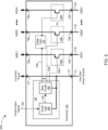
- FIG. 2 is an example circuit arrangement 200 of an active silicon interposer, such as interposer 130 of FIG. 1 .
- interposer 130 is receiving power on the substrate-facing side of the interposer 130 from a core rail power source for the core power rail 111, as well as receiving power from other input power sources VDD1, VDD2, VDDn, etc., for the sequencing power rails 113a, 113b, 113n, etc., respectively.
- the interposer 130 is operable to providing power output on the ASIC-facing side of the interposer 130 for core rail power for the core power rail 111, as well as providing output power VDD1', VDD2', VDDn', etc., to other components for the sequencing power rails 113a, 113b, 113n, etc., respectively.
- the switch control circuitry 134 includes control logic 204 and delay circuitry 206.
- the control logic 204 and delay circuitry 206 each include a power input to receive the core power from the core power rail 111.
- the controller 144 also receives power from the control core power rail 111, and thus is not required to be "switched on.”
- the control logic 204 includes a control input that receives a control input signal 202 (e.g., control input signal 145 from FIG. 1 ) that is received by the switch control circuitry 134 from a sequencer circuit (e.g., controller 144 of the ASIC 140, or an on-board controller on the circuit board 110 as further described herein with reference to FIG. 3 ).
- the controller 144 generates control signals so that that ASIC 140 may be powered up according to a controlled power sequence, e.g., rails may be powered in a specific pre-defined sequence that ensures the ASIC 140, once completely powered up, will operate according to specification and without power-induced errors.
- the control logic 204 provides an output signal 205 to an input of the delay circuitry 206.
- the delay circuitry then generates the switch signals 136a, 136b, 136n, etc., for each respective switch 132a, 132b, 132n, etc., according to a power sequencing process received in the control input signal 202.
- the switch signals 136 include a first state and a second state.
- the switch when the switch signal is in a first state, the switch is in a closed position to electrically connect the first terminal to the second terminal, and when the switch signal is in a second state the switch is in an open position to electrically isolate the first terminal from the second terminal.
- the control logic can be implemented by any appropriate control circuitry that provides switch signals for switches.
- each switch 132a, 132b, 132n includes a first terminal, a second terminal, and a third terminal.
- the third terminal of the each switch receives a control signal that places the first switch in either a closed state in which a conduction path is established between the first and second terminals, or an open state in which the conduction path is eliminated between the first and second terminals.
- the switches 132 or referred to as power gates, turn on and off individual power rails.
- switch 132a is used to switch the power on and off from the power rail 113a (e.g., VDD1) from the power connector 133a on the substrate-facing side of the interposer 130 to the power connector 135a on the ASIC-facing side of the interposer 130.
- switch 132a receives switch signal 136a at the third terminal of the switch 132a that places the switch 132a in a closed state in which a conduction path is established between the first and second terminals of switch 132a, and the output power VDD1' is now provided as an output from the power connector 135a to a connecting device, such as ASIC 140 in FIG. 1 .
- switch 132a receives switch signal 136a at the third terminal of the switch 132a that places the switch 132a in an open state in which the conduction path is eliminated between the first and second terminals of switch 132a, and the power VDD1 is now prohibited as an output from the power connector 135a to a connecting device, such as ASIC 140 in FIG. 1 .
- the interposer 130 includes one or more charge pumps used to elevate the driving voltage of the switch signals 136 and fully open the switches 132.
- charge pump 210 is connected to switch signal 136n.
- the charge pump 210 can boost the voltage for the switch signal 136n in order to provide a voltage that enables switch 132n is fully open to provide the expected power from the power rail 113n (VDDn) to a component that is electrically connected to the ASIC-facing side of the interposer 130, such as ASIC 140 in FIG. 1 .
- the charge pump 210 ensures that the input power received at power connector 133n (VDDn) is substantially similar to the output power at power connector 135n (VDDn').
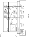
- FIG. 3 is a block diagram of an example integrated power sequencing circuit in a silicon interposer.
- FIG. 3 is an example apparatus 300 includes a sequencer circuit that controls switch signals through a controller on a circuit board.
- the apparatus 300 has a topology similar to apparatus 100 shown in FIG. 1 , except that an on-board controller 316 on the circuit board 310 provides the control input signal 317 to the switch control circuitry 134, instead of the control input signal 145 from the controller 144 of the ASIC 140 as in FIG. 1 .
- the on-board controller 316 also referred to as a sequencer circuit, is electrically connected to core power rail 111 from the power source 112.
- the core power rail is typically the first rail from the circuit board 310, and is also the first rail to turn on in the power rail sequencing process, and powers the integrated chip manager inside the on-board controller 316, which then executes the chip firmware, communicates with the switch control circuitry 134, and manages the rest of the sequencing process, as described herein.
- Embodiments of the subject matter and the operations described in this specification can be implemented in digital electronic circuitry, or in computer software, firmware, or hardware, including the structures disclosed in this specification and their structural equivalents, or in combinations of one or more of them.
- Embodiments of the subject matter described in this specification can be implemented as one or more computer programs, i.e., one or more modules of computer program instructions, encoded on computer storage medium for execution by, or to control the operation of, data processing apparatus.
- An exemplary embodiment can be summarized as an apparatus that includes an interposer, first power connectors that are disposed on a first surface and that receive respective power inputs from one or more power sources, second power connectors that are disposed on the second surface and that receive a respective third power connecter of an integrated circuit when the integrated circuit is mounted on the second surface of the interposer, a plurality of switches formed within the interposer, control circuitry formed within the interposer, and a sequencer circuit coupled to the control input of the control circuitry and that generates a different values for a control input signal that causes the control logic of the control circuitry to generate a corresponding set of switch signals, and the plurality of different values for the control input signal are generated according to a predefined sequence to provide power to the integrated circuit according to power up sequence.
- Example 1 An apparatus, comprising:
- Example 2 The apparatus of example 1, wherein:
- Example 3 The apparatus of example 1, wherein
- Example 4 The apparatus of one of examples 1 to 3, further comprising:
- Example 5 The apparatus of one of examples 1 to 4, further comprising a charge pump circuit that boosts an input voltage of a switch signal for a particular switch and provides the boosted input voltage of the switch signal to a switch control input of the particular switch.
- Example 6 The apparatus of one of examples 1 to 5, wherein the switches are MOSFETs.
Landscapes
- Engineering & Computer Science (AREA)
- Theoretical Computer Science (AREA)
- Power Engineering (AREA)
- Physics & Mathematics (AREA)
- General Engineering & Computer Science (AREA)
- General Physics & Mathematics (AREA)
- Human Computer Interaction (AREA)
- Dc-Dc Converters (AREA)
- Semiconductor Integrated Circuits (AREA)
- Electronic Switches (AREA)
- Power Sources (AREA)
- Logic Circuits (AREA)
Applications Claiming Priority (2)
| Application Number | Priority Date | Filing Date | Title |
|---|---|---|---|
| US16/527,569 US10742211B1 (en) | 2019-07-31 | 2019-07-31 | Power sequencing in an active silicon interposer |
| EP20188629.8A EP3771962B1 (de) | 2019-07-31 | 2020-07-30 | Leistungssequenzierung in einem aktiven silizium-interposer |
Related Parent Applications (2)
| Application Number | Title | Priority Date | Filing Date |
|---|---|---|---|
| EP20188629.8A Division EP3771962B1 (de) | 2019-07-31 | 2020-07-30 | Leistungssequenzierung in einem aktiven silizium-interposer |
| EP20188629.8A Division-Into EP3771962B1 (de) | 2019-07-31 | 2020-07-30 | Leistungssequenzierung in einem aktiven silizium-interposer |
Publications (2)
| Publication Number | Publication Date |
|---|---|
| EP4407407A2 true EP4407407A2 (de) | 2024-07-31 |
| EP4407407A3 EP4407407A3 (de) | 2024-10-30 |
Family
ID=71894686
Family Applications (2)
| Application Number | Title | Priority Date | Filing Date |
|---|---|---|---|
| EP24182119.8A Pending EP4407407A3 (de) | 2019-07-31 | 2020-07-30 | Leistungssequenzierung in einem aktiven silizium-interposer |
| EP20188629.8A Active EP3771962B1 (de) | 2019-07-31 | 2020-07-30 | Leistungssequenzierung in einem aktiven silizium-interposer |
Family Applications After (1)
| Application Number | Title | Priority Date | Filing Date |
|---|---|---|---|
| EP20188629.8A Active EP3771962B1 (de) | 2019-07-31 | 2020-07-30 | Leistungssequenzierung in einem aktiven silizium-interposer |
Country Status (6)
| Country | Link |
|---|---|
| US (2) | US10742211B1 (de) |
| EP (2) | EP4407407A3 (de) |
| CN (2) | CN112305985B (de) |
| DK (1) | DK3771962T3 (de) |
| FI (1) | FI3771962T3 (de) |
| TW (2) | TWI749666B (de) |
Families Citing this family (4)
| Publication number | Priority date | Publication date | Assignee | Title |
|---|---|---|---|---|
| US12471235B2 (en) * | 2021-03-24 | 2025-11-11 | Fanuc Corporation | Electronic apparatus |
| US20230223402A1 (en) * | 2022-01-12 | 2023-07-13 | Kneron Inc. | Three-dimensional Integrated Circuit |
| US12389527B2 (en) | 2023-08-07 | 2025-08-12 | Ciena Corporation | ASIC busbar with remote power phases for telecommunications and networking shelf and circuit card assemblies |
| EP4672883A3 (de) * | 2023-08-07 | 2026-03-25 | Ciena Corporation | Asic-sammelschiene mit entfernten leistungsphasen für telekommunikation und vernetzungsregal- und schaltungskartenanordnungen |
Family Cites Families (25)
| Publication number | Priority date | Publication date | Assignee | Title |
|---|---|---|---|---|
| EP0552288A1 (de) * | 1990-10-03 | 1993-07-28 | Thinking Machines Corporation | Paralleles rechnersystem |
| CN2718635Y (zh) * | 2004-03-03 | 2005-08-17 | 中兴通讯股份有限公司 | 多电源上电顺序控制电路 |
| CN100492228C (zh) * | 2005-05-30 | 2009-05-27 | 杭州华三通信技术有限公司 | 控制多电压上电顺序的装置及方法 |
| US7574540B2 (en) * | 2006-01-03 | 2009-08-11 | Emc Corporation | Managing management controller communications |
| KR100806127B1 (ko) * | 2006-09-06 | 2008-02-22 | 삼성전자주식회사 | 피크 커런트를 감소시키는 파워 게이팅 회로 및 파워게이팅 방법 |
| US7977822B2 (en) | 2007-11-05 | 2011-07-12 | Arm Limited | Dynamically changing control of sequenced power gating |
| US7898072B2 (en) * | 2008-07-11 | 2011-03-01 | Stats Chippac Ltd. | Package stacking system with mold contamination prevention |
| US8907462B2 (en) * | 2009-02-05 | 2014-12-09 | Hewlett-Packard Development Company, L. P. | Integrated circuit package |
| US8680710B2 (en) * | 2010-12-17 | 2014-03-25 | Texas Instruments Incorporated | Analog power sequencer and method |
| US9153508B2 (en) * | 2011-08-17 | 2015-10-06 | Rambus Inc. | Multi-chip package and interposer with signal line compression |
| US8873320B2 (en) * | 2011-08-17 | 2014-10-28 | Taiwan Semiconductor Manufacturing Co., Ltd. | DRAM repair architecture for wide I/O DRAM based 2.5D/3D system chips |
| US8751836B1 (en) * | 2011-12-28 | 2014-06-10 | Datadirect Networks, Inc. | Data storage system and method for monitoring and controlling the power budget in a drive enclosure housing data storage devices |
| US9633872B2 (en) * | 2013-01-29 | 2017-04-25 | Altera Corporation | Integrated circuit package with active interposer |
| US9106229B1 (en) * | 2013-03-14 | 2015-08-11 | Altera Corporation | Programmable interposer circuitry |
| US9059696B1 (en) * | 2013-08-01 | 2015-06-16 | Altera Corporation | Interposer with programmable power gating granularity |
| US9389674B2 (en) * | 2013-09-13 | 2016-07-12 | International Business Machines Corporation | Predictively turning off a charge pump supplying voltage for overdriving gates of the power switch header in a microprocessor with power gating |
| US9298253B2 (en) * | 2013-09-13 | 2016-03-29 | Globalfoundries Inc. | Accelerating the microprocessor core wakeup by predictively executing a subset of the power-up sequence |
| JP6495698B2 (ja) * | 2014-03-20 | 2019-04-03 | 株式会社半導体エネルギー研究所 | 半導体装置、電子部品、及び電子機器 |
| JP6417781B2 (ja) * | 2014-08-13 | 2018-11-07 | 株式会社ソシオネクスト | 半導体装置 |
| US9935052B1 (en) | 2014-11-26 | 2018-04-03 | Altera Corporation | Power line layout in integrated circuits |
| TW201643772A (zh) | 2015-06-08 | 2016-12-16 | 指紋卡公司 | 具有中介結構的指紋感測裝置 |
| CN105786144B (zh) * | 2016-02-02 | 2019-03-15 | 广东技术师范学院 | 一种处理器多电源管理控制装置、系统及方法 |
| US10665579B2 (en) * | 2016-02-16 | 2020-05-26 | Xilinx, Inc. | Chip package assembly with power management integrated circuit and integrated circuit die |
| US9917517B1 (en) * | 2016-10-26 | 2018-03-13 | Google Inc. | Switched tank converter |
| US11036660B2 (en) * | 2019-03-28 | 2021-06-15 | Intel Corporation | Network-on-chip for inter-die and intra-die communication in modularized integrated circuit devices |
-
2019
- 2019-07-31 US US16/527,569 patent/US10742211B1/en active Active
-
2020
- 2020-07-06 US US16/921,571 patent/US11552634B2/en active Active
- 2020-07-27 TW TW109125275A patent/TWI749666B/zh active
- 2020-07-27 TW TW110141976A patent/TWI800087B/zh active
- 2020-07-30 CN CN202010748713.1A patent/CN112305985B/zh active Active
- 2020-07-30 EP EP24182119.8A patent/EP4407407A3/de active Pending
- 2020-07-30 EP EP20188629.8A patent/EP3771962B1/de active Active
- 2020-07-30 DK DK20188629.8T patent/DK3771962T3/da active
- 2020-07-30 CN CN202411003268.0A patent/CN118963518A/zh active Pending
- 2020-07-30 FI FIEP20188629.8T patent/FI3771962T3/fi active
Also Published As
| Publication number | Publication date |
|---|---|
| CN118963518A (zh) | 2024-11-15 |
| DK3771962T3 (da) | 2024-12-02 |
| CN112305985B (zh) | 2024-08-23 |
| EP3771962B1 (de) | 2024-09-04 |
| EP3771962A1 (de) | 2021-02-03 |
| US10742211B1 (en) | 2020-08-11 |
| CN112305985A (zh) | 2021-02-02 |
| EP4407407A3 (de) | 2024-10-30 |
| TW202226758A (zh) | 2022-07-01 |
| US11552634B2 (en) | 2023-01-10 |
| US20210036702A1 (en) | 2021-02-04 |
| TWI800087B (zh) | 2023-04-21 |
| TW202123611A (zh) | 2021-06-16 |
| TWI749666B (zh) | 2021-12-11 |
| FI3771962T3 (fi) | 2024-12-07 |
Similar Documents
| Publication | Publication Date | Title |
|---|---|---|
| EP3771962B1 (de) | Leistungssequenzierung in einem aktiven silizium-interposer | |
| CN102396030B (zh) | 用于降低大的存储器覆盖区背景下的迹线长度和电容的方法和系统 | |
| US9276335B2 (en) | Double-sided circuit board with opposing modular card connector assemblies | |
| US12366882B2 (en) | Field programmable platform array | |
| US6661690B2 (en) | High capacity memory module with built-in performance enhancing features | |
| US11564317B2 (en) | Integrated power delivery board for delivering power to an ASIC with bypass of signal vias in a printed circuit board | |
| US20150359099A1 (en) | Low area over-head connectivity solutions to sip module | |
| JPH0477469B2 (de) | ||
| CN110717569A (zh) | 存储卡、存储卡插槽和电子系统 | |
| US6496380B1 (en) | High capacity memory module with high electrical design margins | |
| HK40042545A (en) | Power sequencing in an active silicon interposer | |
| HK40042545B (zh) | 有源硅中介层中的电源定序 | |
| JP3181710B2 (ja) | 多層プリント回路基板モジュールおよび多層プリント回路基板装置 | |
| HK40119300A (zh) | 有源硅中介层中的电源定序 | |
| US5598035A (en) | Integrated circuit package with external storage capacitor for improved signal quality for sensitive integrated circuit elements | |
| US8837163B2 (en) | Integrated flex tail circuit packaging | |
| JPH03121501A (ja) | 制御装置 | |
| JP2007128959A (ja) | 半導体メモリカードおよび回路基板 | |
| US20080112142A1 (en) | Memory module comprising memory devices | |
| CN115810606A (zh) | 电子设备、电路板和半导体装置 | |
| JP2009010410A (ja) | 半導体装置 | |
| JPH0668942A (ja) | カードエッジコネクタ | |
| JPH10283076A (ja) | 実装状態検出回路 | |
| JP2006245613A (ja) | 半導体装置 | |
| JP2018049956A (ja) | 半導体装置 |
Legal Events
| Date | Code | Title | Description |
|---|---|---|---|
| PUAI | Public reference made under article 153(3) epc to a published international application that has entered the european phase |
Free format text: ORIGINAL CODE: 0009012 |
|
| STAA | Information on the status of an ep patent application or granted ep patent |
Free format text: STATUS: THE APPLICATION HAS BEEN PUBLISHED |
|
| AC | Divisional application: reference to earlier application |
Ref document number: 3771962 Country of ref document: EP Kind code of ref document: P |
|
| AK | Designated contracting states |
Kind code of ref document: A2 Designated state(s): AL AT BE BG CH CY CZ DE DK EE ES FI FR GB GR HR HU IE IS IT LI LT LU LV MC MK MT NL NO PL PT RO RS SE SI SK SM TR |
|
| REG | Reference to a national code |
Ref country code: DE Ref legal event code: R079 Free format text: PREVIOUS MAIN CLASS: G06F0001180000 Ipc: G06F0001260000 |
|
| PUAL | Search report despatched |
Free format text: ORIGINAL CODE: 0009013 |
|
| AK | Designated contracting states |
Kind code of ref document: A3 Designated state(s): AL AT BE BG CH CY CZ DE DK EE ES FI FR GB GR HR HU IE IS IT LI LT LU LV MC MK MT NL NO PL PT RO RS SE SI SK SM TR |
|
| RIC1 | Information provided on ipc code assigned before grant |
Ipc: G06F 1/18 20060101ALI20240924BHEP Ipc: G06F 1/26 20060101AFI20240924BHEP |
|
| STAA | Information on the status of an ep patent application or granted ep patent |
Free format text: STATUS: REQUEST FOR EXAMINATION WAS MADE |
|
| 17P | Request for examination filed |
Effective date: 20250403 |
|
| STAA | Information on the status of an ep patent application or granted ep patent |
Free format text: STATUS: EXAMINATION IS IN PROGRESS |
|
| 17Q | First examination report despatched |
Effective date: 20250625 |
|
| GRAP | Despatch of communication of intention to grant a patent |
Free format text: ORIGINAL CODE: EPIDOSNIGR1 |
|
| STAA | Information on the status of an ep patent application or granted ep patent |
Free format text: STATUS: GRANT OF PATENT IS INTENDED |
|
| INTG | Intention to grant announced |
Effective date: 20260122 |