EP4404277A1 - Schottky-sperrschichtdiode - Google Patents
Schottky-sperrschichtdiode Download PDFInfo
- Publication number
- EP4404277A1 EP4404277A1 EP23793984.8A EP23793984A EP4404277A1 EP 4404277 A1 EP4404277 A1 EP 4404277A1 EP 23793984 A EP23793984 A EP 23793984A EP 4404277 A1 EP4404277 A1 EP 4404277A1
- Authority
- EP
- European Patent Office
- Prior art keywords
- layer
- silicide
- silicide layer
- schottky barrier
- silicon
- Prior art date
- Legal status (The legal status is an assumption and is not a legal conclusion. Google has not performed a legal analysis and makes no representation as to the accuracy of the status listed.)
- Pending
Links
Images

Classifications
-
- H—ELECTRICITY
- H10—SEMICONDUCTOR DEVICES; ELECTRIC SOLID-STATE DEVICES NOT OTHERWISE PROVIDED FOR
- H10D—INORGANIC ELECTRIC SEMICONDUCTOR DEVICES
- H10D62/00—Semiconductor bodies, or regions thereof, of devices having potential barriers
- H10D62/10—Shapes, relative sizes or dispositions of the regions of the semiconductor bodies; Shapes of the semiconductor bodies
- H10D62/102—Constructional design considerations for preventing surface leakage or controlling electric field concentration
- H10D62/103—Constructional design considerations for preventing surface leakage or controlling electric field concentration for increasing or controlling the breakdown voltage of reverse-biased devices
- H10D62/105—Constructional design considerations for preventing surface leakage or controlling electric field concentration for increasing or controlling the breakdown voltage of reverse-biased devices by having particular doping profiles, shapes or arrangements of PN junctions; by having supplementary regions, e.g. junction termination extension [JTE]
- H10D62/106—Constructional design considerations for preventing surface leakage or controlling electric field concentration for increasing or controlling the breakdown voltage of reverse-biased devices by having particular doping profiles, shapes or arrangements of PN junctions; by having supplementary regions, e.g. junction termination extension [JTE] having supplementary regions doped oppositely to or in rectifying contact with regions of the semiconductor bodies, e.g. guard rings with PN or Schottky junctions
- H10D62/107—Buried supplementary regions, e.g. buried guard rings
-
- H—ELECTRICITY
- H10—SEMICONDUCTOR DEVICES; ELECTRIC SOLID-STATE DEVICES NOT OTHERWISE PROVIDED FOR
- H10D—INORGANIC ELECTRIC SEMICONDUCTOR DEVICES
- H10D64/00—Electrodes of devices having potential barriers
- H10D64/60—Electrodes characterised by their materials
- H10D64/64—Electrodes comprising a Schottky barrier to a semiconductor
-
- H—ELECTRICITY
- H10—SEMICONDUCTOR DEVICES; ELECTRIC SOLID-STATE DEVICES NOT OTHERWISE PROVIDED FOR
- H10D—INORGANIC ELECTRIC SEMICONDUCTOR DEVICES
- H10D8/00—Diodes
- H10D8/01—Manufacture or treatment
- H10D8/051—Manufacture or treatment of Schottky diodes
-
- H—ELECTRICITY
- H10—SEMICONDUCTOR DEVICES; ELECTRIC SOLID-STATE DEVICES NOT OTHERWISE PROVIDED FOR
- H10D—INORGANIC ELECTRIC SEMICONDUCTOR DEVICES
- H10D8/00—Diodes
- H10D8/60—Schottky-barrier diodes
-
- H—ELECTRICITY
- H10—SEMICONDUCTOR DEVICES; ELECTRIC SOLID-STATE DEVICES NOT OTHERWISE PROVIDED FOR
- H10D—INORGANIC ELECTRIC SEMICONDUCTOR DEVICES
- H10D8/00—Diodes
- H10D8/60—Schottky-barrier diodes
- H10D8/605—Schottky-barrier diodes of the trench conductor-insulator-semiconductor barrier type, e.g. trench MOS barrier Schottky rectifiers [TMBS]
-
- H—ELECTRICITY
- H10—SEMICONDUCTOR DEVICES; ELECTRIC SOLID-STATE DEVICES NOT OTHERWISE PROVIDED FOR
- H10D—INORGANIC ELECTRIC SEMICONDUCTOR DEVICES
- H10D62/00—Semiconductor bodies, or regions thereof, of devices having potential barriers
- H10D62/10—Shapes, relative sizes or dispositions of the regions of the semiconductor bodies; Shapes of the semiconductor bodies
- H10D62/102—Constructional design considerations for preventing surface leakage or controlling electric field concentration
- H10D62/103—Constructional design considerations for preventing surface leakage or controlling electric field concentration for increasing or controlling the breakdown voltage of reverse-biased devices
- H10D62/105—Constructional design considerations for preventing surface leakage or controlling electric field concentration for increasing or controlling the breakdown voltage of reverse-biased devices by having particular doping profiles, shapes or arrangements of PN junctions; by having supplementary regions, e.g. junction termination extension [JTE]
- H10D62/106—Constructional design considerations for preventing surface leakage or controlling electric field concentration for increasing or controlling the breakdown voltage of reverse-biased devices by having particular doping profiles, shapes or arrangements of PN junctions; by having supplementary regions, e.g. junction termination extension [JTE] having supplementary regions doped oppositely to or in rectifying contact with regions of the semiconductor bodies, e.g. guard rings with PN or Schottky junctions
-
- H—ELECTRICITY
- H10—SEMICONDUCTOR DEVICES; ELECTRIC SOLID-STATE DEVICES NOT OTHERWISE PROVIDED FOR
- H10D—INORGANIC ELECTRIC SEMICONDUCTOR DEVICES
- H10D62/00—Semiconductor bodies, or regions thereof, of devices having potential barriers
- H10D62/10—Shapes, relative sizes or dispositions of the regions of the semiconductor bodies; Shapes of the semiconductor bodies
- H10D62/102—Constructional design considerations for preventing surface leakage or controlling electric field concentration
- H10D62/112—Constructional design considerations for preventing surface leakage or controlling electric field concentration for preventing surface leakage due to surface inversion layers, e.g. by using channel stoppers
Definitions
- the present invention relates to a Schottky barrier diode.
- the Schottky barrier diode is a diode having rectifying properties by utilizing a Schottky barrier formed at a contact portion between a metal and a semiconductor. Since the Schottky barrier diode has an extremely small amount of accumulated charges in carriers, the Schottky barrier diode has characteristics in that turn-on time and turn-off time are extremely short. Accordingly, the Schottky barrier diode is used in many applications such as detection and mixer, high-speed switching, and rectification on a secondary side of power supplies. A technique related to this is disclosed in Japanese Patent No. 3983689 .
- the performance of a diode is expressed by characteristic values of a forward voltage VF that is a voltage applied in a direction from an anode to a cathode, and a reverse current IR that is a minute current flowing when applying a reverse voltage in a direction from the cathode to the anode.
- VF of the Schottky barrier diode is smaller in comparison to a typical PN diode.
- the Schottky barrier diode may be required to have various values of Schottky barrier heights ( ⁇ Bn) so as to obtain desired characteristics.
- An object of various aspects of the invention is to provide a Schottky barrier diode capable of controlling a Schottky barrier height ( ⁇ Bn) to various values, and a manufacturing method thereof.
- a Schottky barrier diode capable of controlling a Schottky barrier height ( ⁇ Bn) to various values.
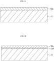
- Fig. 1 is a cross-sectional view illustrating a Schottky barrier diode according to an aspect of the invention.
- the Schottky barrier diode in Fig. 1 includes a silicon layer 11, and a silicide layer 12a containing Pt and Ni is disposed on the silicon layer 11. A junction between the silicon layer 11 and the silicide layer 12a forms a Schottky junction.
- a peak value of a concentration of Pt in the silicide layer 12a with a thickness of 50 nm on the silicide layer 12a side from an interface between the silicide layer 12a and the silicon layer 11, or a peak value of the concentration of Pt in the silicide layer 12a in a case where the thickness of the silicide layer 12a is less than 50 nm may be 1 at% to 60 at%, preferably 50 at% or less, more preferably 40 at% or less, still more preferably 30 at% or less, yet more preferably 20 at% or less, and even more preferably 10 at% or less (or 7 at% or less, 5.5 at% or less, or 4 at% or less).
- the peak value of the concentration of Pt may occur at the interface or on an interface side in the silicide layer 12a.
- the silicide layer 12a containing Pt and Ni is disposed on the silicon layer 11, and proportions and a concentration distribution of Pt and Ni contained in the silicide layer 12a are adjusted so that the peak value or the like of the concentration of Pt in the silicide layer 12a with a thickness of 50 nm on the silicide layer 12a side from the interface between the silicide layer 12a and the silicon layer 11 becomes 1 at% to 60 at% or the like.
- the Schottky barrier height ( ⁇ Bn) occurring at the interface between a metal and a semiconductor can be controlled to various values, and as a result, desired characteristics in the Schottky barrier diode can be obtained.
- a silicon substrate 10 is disposed below the silicon layer 11, and the silicon layer 11 is, for example, an epitaxial layer formed on the silicon substrate 10.
- a rear electrode 21 is formed on a rear surface of the silicon substrate 10, and a metal such as Ni, Ti, Au, Ag, and Al may be used as the rear electrode 21.
- a PtNi alloy layer 12 is disposed on the silicide layer 12a. Note that, in this embodiment, the PtNi alloy layer 12 is disposed on the silicide layer 12a, but a mixed layer of Pt and Ni may be disposed on the silicide layer 12a.
- the silicide layer 12a containing Pt and Ni may be disposed on the silicon layer 11, and Pt may be contained at an interface between the silicide layer 12a and the silicon layer 11.
- the Schottky barrier height ( ⁇ Bn) can be controlled to various values by adjusting proportions and a concentration distribution of Pt and Ni contained in the silicide layer 12a, and as a result, desired characteristics in the Schottky barrier diode can be obtained.
- a guard ring 20 located below an end of the PtNi alloy layer 12 is disposed inside the silicon layer 11.
- a withstand voltage of the Schottky barrier diode can be raised due to the guard ring 20.
- a first laminated structure layer 19 is formed on the PtNi alloy layer 12, and the first laminated structure layer 19 is a layer in which an Al layer 13 and a Ni layer 14 are sequentially laminated.
- the first laminated structure layer 19 is formed on the PtNi alloy layer 12, but as illustrated in Fig. 2 , a second laminated structure layer 18 may be formed on the PtNi alloy layer 12, and the second laminated structure layer 18 is a layer in which the Ni layer 14 and the Al layer 13 are sequentially laminated.
- Fig. 2 is a cross-sectional view illustrating a first modification example of the Schottky barrier diode illustrated in Fig. 1 , and is similar to the Schottky barrier diode illustrated in Fig. 1 except that the first laminated structure layer 19 is modified to the second laminated structure layer 18.
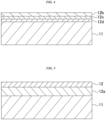
- a channel stopper layer 31 located on an outer side of the guard ring 20 is formed to be separated from the guard ring 20.
- the channel stopper layer 31 is formed in a ring shape.
- a passivation layer 32 is formed on the silicon layer 11 and on an outer side of the PtNi alloy layer 12, and the passivation layer 32 is in contact with the PtNi alloy layer 12 and is located between the guard ring 20 and the channel stopper layer 31.
- the passivation layer 32 for example, an SiO 2 layer, a phosphorous silicate glass (PSG) layer, or an Si 3 N 4 layer can be used.
- a Ti layer 34 is formed between both the PtNi alloy layer 12 and the passivation layer 32, and the first laminated structure layer 19. Note that, in this embodiment, the Ti layer 34 is formed between both the PtNi alloy layer 12 and the passivation layer 32, and the first laminated structure layer 19, but a modification can be made so that the Ti layer 34 is not formed and the first laminated structure layer 19 may be formed on both the PtNi alloy layer 12 and the passivation layer 32.
- a polyimide film 33 as a protective film is formed on side walls of the channel stopper layer 31, the Ti layer 34, and the first laminated structure layer 19, and on the first laminated structure layer 19, but the polyimide film 33 is not formed at the center of an upper surface of the first laminated structure layer 19.
- the PtNi alloy layer 12 is formed between the silicide layer 12a containing Pt and Ni and the Ti layer 34, but a modification may be made so that the PtNi alloy layer 12 is removed and the Ti layer 34 is formed on the silicide layer 12a containing Pt and Ni, or preparation may be performed so that the PtNi alloy layer 12 may not be formed by forming the silicide layer 12a containing Pt and Ni.
- the silicide layer 12a containing Pt and Ni is disposed on the silicon layer 11, and Pt is contained at an interface between the silicide layer 12a and the silicon layer 11.
- proportions and a concentration distribution of Pt and Ni contained in the silicide layer 12a are adjusted so that a peak value of the concentration of Pt in the silicide layer 12a with a thickness of 50 nm on the silicide layer 12a side from the interface between the silicide layer 12a and the silicon layer 11, or a peak value of the concentration of Pt in the silicide layer 12a in a case where the thickness of the silicide layer 12a is less than 50 nm becomes 1 at% to 60 at%.
- a Schottky barrier height ( ⁇ Bn) can be controlled to various values, and as a result, desired characteristics in the Schottky barrier diode can be obtained.
- the Ti layer 34 is formed on the PtNi alloy layer 12, but a modification may be made so that a Mo layer instead of the Ti layer 34 is formed on the PtNi alloy layer 12.
- the Ti layer 34 is formed on the PtNi alloy layer 12, but a modification may be made so that a Mo layer is formed on the Ti layer 34. That is, the Ti layer 34 and the Mo layer may be formed between the PtNi alloy layer 12 and the first laminated structure layer 19.
- the Ti layer 34 is formed on the PtNi alloy layer 12, but a modification may be made so that a laminated film instead of the Ti layer 34 is formed on the PtNi alloy layer 12, and the laminated film is a film in which at least two films among an Al film, a Ni film, and a Mo film are laminated.
- a method of manufacturing a Schottky barrier diode according to another aspect of the invention will be described with reference to Fig. 1 , Figs. 3A and 3B , Fig. 4, and Fig. 5 .
- Figs. 3A and 3B , Fig. 4, and Fig. 5 are cross-sectional views describing a method of preparing a Schottky junction portion illustrated in Fig. 1 .
- the silicon layer 11 is formed on the silicon substrate 10.
- the silicon layer 11 is, for example, an epitaxial layer.
- an oxide film (not illustrated) is formed on a surface of the silicon layer 11, and the guard ring layer 20 is formed on the silicon layer 11.
- the channel stopper layer 31 is formed in the silicon layer 11.
- the passivation layer 32 is formed on the silicon layer 11.
- an oxide film of a Schottky junction surface of the silicon layer 11 is removed through etching (not illustrated).
- a Pt layer 12c is formed on the silicon layer 11 including the Schottky junction surface (process (a)).
- a heat treatment is performed on the Pt layer 12c and the silicon layer 11 at a temperature of 150°C to 300°C to form a Pt silicide layer 12d on the silicon layer 11 as illustrated in Fig. 3B (process (b)).
- the Pt layer 12c that is not silicided remains on the Pt silicide layer 12d. Note that, in this embodiment, the Pt layer 12c that is not silicided remains on the Pt silicide layer 12d, but the Pt layer 12c that is not silicided may not remain on the Pt silicide layer 12d.
- a Ni layer 12b is formed on the Pt silicide layer 12d and the Pt layer 12c (process (c)).
- the Ti layer 34 is formed on the Ni layer 12b. Note that, in this embodiment, the Ti layer 34 is formed, but the process may proceed to the subsequent process without forming the Ti layer 34.
- each of the Pt layer 12c, the Ni layer 12b, and the Ti layer 34 may be formed by using any film forming method among a vapor deposition method, a sputtering method, and a CVD method.
- a heat treatment is performed on the silicon layer 11, the Pt silicide layer 12d, the Pt layer 12c, and the Ni layer 12b at a temperature of 300°C to 600°C.
- the silicide layer 12a containing Pt and Ni is formed on the silicon layer 11, and the PtNi alloy layer 12 or the mixed layer of Pt and Ni is formed on the silicide layer 12a as illustrated in Fig. 5 (process (d)).
- a peak value of the concentration of Pt in the silicide layer with a thickness of 50 nm on the silicide layer side from the interface between the silicide layer 12a and the silicon layer 11, or a peak value of the concentration of Pt in the silicide layer 12a in a case where the thickness of the silicide layer 12a is less than 50 nm can be set to 1 at% to 60 at% by adjusting the thicknesses of the Pt layer 12c and the Ni layer 12b and a ratio of the thicknesses.
- the Pt layer 12c is formed on the silicon layer 11 before forming the silicide layer 12a containing Pt and Ni, and a heat treatment is performed on the Pt layer 12c and the silicon layer 11 at a temperature of 150°C to 300°C to form the Pt silicide layer 12d on the silicon layer 11.
- the peak value of the concentration of Pt in the subsequently formed silicide layer 12a with a thickness of 50 nm on the silicide layer 12a side from the interface between the silicide layer 12a containing Pt and Ni and the silicon layer 11, or the peak value of the concentration of Pt in the silicide layer 12a in a case where the thickness of the silicide layer is less than 50 nm can be set to 1 at% to 60 at%.
- the peak value of the concentration of Pt can be caused to occur at the interface between the silicide layer 12a and the silicon layer 11 or on the interface side in the silicide layer 12a.
- the Schottky barrier height ( ⁇ Bn) can be controlled to various values, and as a result, desired characteristics in the Schottky barrier diode can be obtained.
- the Al layer 13 is formed on the Ti layer 34, and the Ni layer 14 is formed on the Al layer 13.
- a photoresist film (not illustrated) is formed on the Ni layer 14, the Al layer 13, and the Ti layer 34, and the Ni layer 14, the Al layer 13, and the Ti layer 34 are etched by using the photoresist film as a mask. According to this, a pattern formed by the Ni layer 14, the Al layer 13, and the Ti layer 34 is formed.
- the Al layer 13 and the Ni layer 14 are also referred to as the first laminated structure layer 19.
- a metal layer as the rear electrode 21 is formed on a rear surface of the silicon substrate 10.
- the metal layer may be formed by a film forming method by a vapor deposition method or a sputtering method.
- the PtNi alloy layer 12 or the mixed layer of Pt and Ni is formed on the silicide layer 12a, the PtNi alloy layer 12 or the mixed layer of Pt and Ni remains, but the PtNi alloy layer 12 or the mixed layer of Pt and Ni may be removed after the PtNi alloy layer 12 is formed on the silicide layer 12a.
- a method of manufacturing a Schottky barrier diode according to still another aspect of the invention will be described with reference to Fig. 1 , Fig. 3B , Fig. 4, and Fig. 5 .
- the silicon layer 11 is formed on the silicon substrate 10, an oxide film (not illustrated) is formed on a surface of the silicon layer 11, the guard ring layer 20 is formed in the silicon layer 11, and the channel stopper layer 31 is formed in the silicon layer 11.
- the passivation layer 32 is formed on the silicon layer 11, and an oxide film of a Schottky junction surface of the silicon layer 11 is removed (not illustrated).
- the Pt layer 12c is formed on the silicon layer 11 while heating the silicon layer 11 including the Schottky junction surface at a temperature of 150°C to 300°C.
- the Pt silicide layer 12d is formed on the silicon layer 11 while forming the Pt layer 12c (process (a)).
- the Pt layer 12c that is not silicided remains on the Pt silicide layer 12d.
- the Pt layer 12c that is not silicided remains on the Pt silicide layer 12d, but the Pt layer 12c that is not silicided may not remain on the Pt silicide layer 12d.
- the Pt layer 12c formed on the passivation film 32 is removed by patterning the Pt layer 12c through etching.
- the Ni layer 12b is formed on the Pt silicide layer 12d and the Pt layer 12c while heating the silicon layer 11 at a temperature of 150°C to 300°C (process (b)).
- the Ni layer may be slightly silicided or may not be silicided.
- each of the Pt layer 12c and the Ni layer 12b may be formed by using any film forming method among a vapor deposition method, a sputtering method, and a CVD method.
- a peak value of the concentration of Pt in the silicide layer with a thickness of 50 nm on the silicide layer side from the interface between the silicide layer 12a and the silicon layer 11, or a peak value of the concentration of Pt in the silicide layer 12a in a case where the thickness of the silicide layer 12a is less than 50 nm can be set to 1 at% to 60 at% by adjusting the thicknesses of the Pt layer 12c and the Ni layer 12b and a ratio of the thicknesses.
- a heat treatment is performed on the silicon layer 11, the Pt silicide layer 12d, the Pt layer 12c, and the Ni layer 12b at a temperature of 300°C to 600°C to form a desired silicide structure on the silicon layer 11 (process (d)).
- the desired silicide structure for example, as illustrated in Fig. 5 , the silicide layer 12a containing Pt and Ni is formed on the silicon layer 11, and the PtNi alloy layer 12 or the mixed layer of Pt and Ni is formed on the silicide layer 12a.
- the Ti layer 34, the Al layer 13, and the Ni layer 14 are sequentially formed on the PtNi alloy layer 12 or the mixed layer of Pt and Ni at a temperature of 100°C to 250°C.
- the Ti layer 34, the Al layer 13, and the Ni layer 14 are sequentially formed on the PtNi alloy layer 12 or the mixed layer of Pt and Ni, but a Ni layer, a Ti layer, a Mo layer, and an Al layer can also be sequentially formed on the PtNi alloy layer 12 or the mixed layer of Pt and Ni at a temperature of 100°C to 250°C.
- the Ni layer 12b is formed on the Pt silicide layer 12d and the Pt layer 12c while heating the silicon layer 11 at a temperature of 150°C to 300°C, but the following modification may be made.
- the Ni layer 12b, the Ti layer 34, the Mo layer, and the Al layer are continuously formed on the Pt silicide layer 12d and the Pt layer 12c while heating the silicon layer 11 at a temperature of 100°C to 250°C (process (b)).
- the Mo layer corresponds to a reference numeral 13 shown in Fig. 1
- the Al layer corresponds to a reference numeral 14 shown in Fig. 1 .
- each of the Pt layer 12c, the Ni layer 12b, the Ti layer 34, the Mo layer, and the Al layer may be formed by using any film forming method among a vapor deposition method, a sputtering method, and a CVD method.
- the Ni layer 12b, the Ti layer 34, the Mo layer, and the Al layer are patterned through etching to remove a part of the Ni layer 12b, the Ti layer 34, the Mo layer, and the Al layer formed on the passivation film 32 (refer to Fig. 1 ).
- a heat treatment is performed on the silicon layer 11, the Pt silicide layer 12d, the Pt layer 12c, the Ni layer 12b, the Ti layer 34, the Mo layer, and the Al layer at a temperature of 300°C to 600°C to form a desired silicide structure on the silicon layer 11 (process (d)).
- the desired silicide structure for example, as illustrated in Fig. 5 , the silicide layer 12a containing Pt and Ni is formed on the silicon layer 11, and the PtNi alloy layer 12 or the mixed layer of Pt and Ni is formed on the silicide layer 12a.
- the PtNi alloy layer 12 or the mixed layer of Pt and Ni may be removed as in the second embodiment.
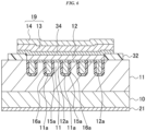
- Fig. 6 is a cross-sectional view illustrating a trench Schottky barrier diode according to still another aspect of the invention, and the same reference numerals will be given the same portion as in Fig. 1 , and description will be given of only a portion different from the first embodiment.
- a plurality of grooves 11a are formed in the silicon layer 11.
- the silicon layer 11 is disposed adjacent to the plurality of grooves 11a.
- An insulator layer 15a is formed on an inner wall of each of the plurality of grooves 11a.
- a conductor layer 16a is disposed in the groove 11a and on the insulator layer 15a.
- the insulator layer 15a for example, an SiO 2 layer formed through thermal oxidization can be used, and as the conductor layer 16a, for example, a polysilicon layer can be used. Note that, in this embodiment, description is given to the trench Schottky barrier diode in which the plurality of grooves 11a are formed, but a trench Schottky barrier diode in which one groove 1 1a is formed can also be used.
- the silicide layer 12a is formed on an upper portion of the conductor layer 16a inside the plurality of grooves 11a. In addition, the silicide layer 12a is formed on a surface of the silicon layer 11 located between the plurality of grooves 11a.
- the grooves 11a are formed in the silicon layer 11, the insulator layer 15a is formed on an inner wall of each of the grooves 11a, the conductor layer 16a is formed inside the groove 11a and on the insulator layer 15a, the silicide layer 12a is formed on an upper portion of the conductor layer 16a, and the silicide layer 12a is formed on a surface of the silicon layer 11 adjacent to the groove 11a.
- the Schottky barrier diode having the trench structure proportions and a concentration distribution of Pt and Ni contained in the silicide layer 12a are adjusted so that a peak value of the concentration of Pt in the silicide layer 12a with a thickness of 50 nm on the silicide layer 12a side from the interface between the silicide layer 12a and the silicon layer 11, or a peak value of the concentration of Pt in the silicide layer 12a in a case where the thickness of the silicide layer 12a is less than 50 nm becomes 1 at% to 60 at%.
- the Schottky barrier height ( ⁇ Bn) can be controlled to various values, and as a result, desired characteristics can be obtained.
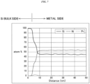
- Fig. 7 is a view illustrating a profile of proportions of respective elements Si, Pt, and Ni in a silicide layer 12a with a thickness of 50 nm on the silicide layer 12a side from an interface between the silicon layer 11 and the silicide layer 12a in a prepared sample of the Schottky barrier diode.
- the profile of the proportions of the respective elements was measured by scanning transmission electron microscope (STEM)/energy dispersive X-ray spectroscopy (EDX).
- a process of preparing the sample is as follows. Note that, the sample will be described with reference to Fig. 1 .
- the silicon layer 11 was formed on the silicon substrate 10 by an epitaxial growth method, and the Pt layer is formed on the silicon layer 11 by a vapor deposition method while heating the silicon substrate at a temperature of 150°C to 300°C.
- the Pt layer is patterned by a photographic process and an etching process.
- the Ni layer is formed by a vapor deposition method at a temperature of 150°C to 300°C.
- any of a Ti layer, a lamination layer of Ti/Al, a lamination layer of Ti/Al or Ni, a lamination layer of Ti/Mo/Al, and a lamination layer of Ti/Mo/Al/Ni is formed on the Ni layer at a temperature of 150°C to 300°C by a vapor deposition method.
- metals other than the Pt layer are patterned by a photographic process and an etching process.
- the silicon substrate 10 and the layers on the silicon substrate 10 are heat-treated (annealed) at a temperature of 300°C to 600°C to form the silicide layer 12a containing Pt and Ni.
- PI polyimide
- PI polyimide
- PI polyimide
- (8) processing such as rear surface grinding and etching of the silicon substrate 10 is performed to obtain a desired silicon substrate thickness.
- a back metal Ti/Ni/Al is formed on a rear surface of the silicon substrate 10. According to this, the rear electrode 21 of the silicon substrate 10 is formed.
- a concentration profile was measured on the silicide layer 12a side from the interface between the silicon layer 11 and the silicide layer 12a prepared as described above with the STEM/EDX.
- a peak value of the concentration of Pt in the silicide layer 12a with a thickness of 50 nm on the silicide layer 12a side from the interface between the silicide layer 12a and the silicon layer 11 was 3 at% or less.
- the peak value of the concentration of Pt was caused to occur at the interface between the silicide layer 12a and the silicon layer 11 or on the interface side in the silicide layer 12a.
- the peak value of the concentration of Pt can be set to 1 at% to 60 at% by adjusting conditions such as the thicknesses and a thickness ratio of the Pt layer 12c and the Ni layer 12b formed on the silicon layer 11 and the annealing temperature. According to this, the Schottky barrier height ( ⁇ Bn) can be controlled to various values, and as a result, desired characteristics in the Schottky barrier diode can be obtained.
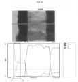
- Fig. 8 is a view illustrating a profile of proportions of the respective elements Si, Pt, and Ni in the silicide layer 12a with a thickness of 50 nm (refer to a reference numeral 32 in Fig. 8 ) on the silicide layer 12a side from the interface (refer to a reference numeral 31 in Fig. 8 ) between the silicon layer 11 and the silicide layer 12a in a prepared sample of the Schottky barrier diode.
- the profile of the proportions of the respective elements was measured by STEM/EDX.
- a process of preparing the sample is as follows. Note that, the sample will be described with reference to Fig. 1 .
- the silicon layer 11 was formed on the silicon substrate 10 by an epitaxial growth method, and a Pt layer is formed on the silicon layer 11 while heated at a temperature of 150°C to 300°C. According to this, a Pt silicide is formed between the Pt layer and the silicon layer 11. In other words, the Pt layer is formed on the silicon layer 11 while forming the Pt silicide.
- the Ni layer is formed at a temperature of 150°C to 300°C. This is continuous vapor deposition (continuous sputtering).
- a lamination layer of Pt/Ni is patterned by a photographic process and etching.
- (4) annealing is performed at a temperature of 300°C to 600°C.
- the silicide layer 12a is formed on the silicon layer 11.
- any of a Ti layer, a lamination layer of Ti/Al, a lamination layer of Ti/Al or Ni, a lamination layer of Ti/Mo/Al, and a lamination layer of Ti/Mo/Al/Ni is formed on the lamination layer of Pt/Ni at a temperature of 150°C to 300°C by a vapor deposition method.
- metals other than the Pt layer are patterned by a photographic process and an etching process.
- polyimide (PI) is applied, and patterning and baking are performed.
- (8) processing such as rear surface grinding and etching of the silicon substrate 10 is performed to obtain a desired silicon substrate thickness.
- a back metal Ti/Ni/Al is formed on a rear surface of the silicon substrate 10. According to this, the rear electrode 21 of the silicon substrate 10 is formed.
- annealing is performed at a temperature of 300°C to 600°C in (4), but the lamination layer of Pt/Ni may be patterned by the photographic process and the etching in (3) after forming the silicide layer 12a on the silicon layer 11 by performing annealing at a temperature of 300°C to 600°C in (4).
- a concentration profile was measured on the silicide layer 12a side from the interface between the silicon layer 11 and the silicide layer 12a prepared as described above with the STEM/EDX.
- a peak value of the concentration of Pt in the silicide layer 12a with a thickness of 50 nm on the silicide layer 12a side from the interface between the silicide layer 12a and the silicon layer 11 was approximately 54 at%.
- the peak value of the concentration of Pt can be set to 1 at% to 60 at% by adjusting conditions such as the thicknesses and a thickness ratio of the Pt layer 12c and the Ni layer 12b formed on the silicon layer 11 and the annealing temperature. According to this, the Schottky barrier height ( ⁇ Bn) can be controlled to various values, and as a result, desired characteristics in the Schottky barrier diode can be obtained.
Landscapes
- Electrodes Of Semiconductors (AREA)
Applications Claiming Priority (2)
| Application Number | Priority Date | Filing Date | Title |
|---|---|---|---|
| JP2022194924 | 2022-12-06 | ||
| PCT/JP2023/022170 WO2024122085A1 (ja) | 2022-12-06 | 2023-06-08 | ショットキーバリアダイオード |
Publications (2)
| Publication Number | Publication Date |
|---|---|
| EP4404277A1 true EP4404277A1 (de) | 2024-07-24 |
| EP4404277A4 EP4404277A4 (de) | 2024-10-23 |
Family
ID=88689499
Family Applications (1)
| Application Number | Title | Priority Date | Filing Date |
|---|---|---|---|
| EP23793984.8A Pending EP4404277A4 (de) | 2022-12-06 | 2023-06-08 | Schottky-sperrschichtdiode |
Country Status (6)
| Country | Link |
|---|---|
| US (1) | US20240379880A1 (de) |
| EP (1) | EP4404277A4 (de) |
| JP (1) | JPWO2024122085A1 (de) |
| CN (1) | CN118451555A (de) |
| TW (1) | TWI900885B (de) |
| WO (1) | WO2024122085A1 (de) |
Families Citing this family (1)
| Publication number | Priority date | Publication date | Assignee | Title |
|---|---|---|---|---|
| CN119486158B (zh) * | 2025-01-16 | 2025-04-22 | 深圳市亚尔讯科技有限公司 | 一种低正向压降的肖特基二极管及其制造方法 |
Family Cites Families (18)
| Publication number | Priority date | Publication date | Assignee | Title |
|---|---|---|---|---|
| US4816879A (en) * | 1982-12-08 | 1989-03-28 | North American Philips Corporation, Signetics Division | Schottky-type rectifier having controllable barrier height |
| JP3983689B2 (ja) * | 2003-02-18 | 2007-09-26 | 新電元工業株式会社 | ショットキーバリアダイオードの製造方法及び絶縁ゲート型バイポーラトランジスタの製造方法 |
| JP2006310555A (ja) * | 2005-04-28 | 2006-11-09 | Nec Electronics Corp | 半導体装置およびその製造方法 |
| US20070123042A1 (en) * | 2005-11-28 | 2007-05-31 | International Business Machines Corporation | Methods to form heterogeneous silicides/germanides in cmos technology |
| US8274128B2 (en) * | 2007-03-23 | 2012-09-25 | Siliconix Technology C. V. Ir | Semiconductor device with buffer layer |
| KR20130014849A (ko) * | 2011-08-01 | 2013-02-12 | 삼성전자주식회사 | 쇼트키 배리어 다이오드 및 이의 제조방법 |
| JP2013102081A (ja) * | 2011-11-09 | 2013-05-23 | Tamura Seisakusho Co Ltd | ショットキーバリアダイオード |
| JP6091941B2 (ja) * | 2012-09-27 | 2017-03-08 | ルネサスエレクトロニクス株式会社 | 半導体装置 |
| JP2014078631A (ja) * | 2012-10-11 | 2014-05-01 | Renesas Electronics Corp | 半導体装置およびその製造方法 |
| CN103681885B (zh) * | 2013-12-18 | 2017-03-29 | 济南市半导体元件实验所 | 肖特基二极管芯片、器件及芯片复合势垒的制备方法 |
| US9263598B2 (en) * | 2014-02-14 | 2016-02-16 | Semiconductor Components Industries, Llc | Schottky device and method of manufacture |
| CN103943495A (zh) * | 2014-03-24 | 2014-07-23 | 吉林麦吉柯半导体有限公司 | 金属与n型硅肖特基接触势垒高度的调节方法 |
| TW201605057A (zh) * | 2014-07-25 | 2016-02-01 | Pan Jit Internat Inc | 溝渠式蕭特基二極體 |
| JP2016213408A (ja) * | 2015-05-13 | 2016-12-15 | 株式会社東芝 | トンネルfet |
| WO2017110940A1 (ja) * | 2015-12-25 | 2017-06-29 | 出光興産株式会社 | 半導体素子及びそれを用いた電気機器 |
| US10651317B2 (en) * | 2016-04-15 | 2020-05-12 | Macom Technology Solutions Holdings, Inc. | High-voltage lateral GaN-on-silicon Schottky diode |
| JP7456220B2 (ja) * | 2020-03-19 | 2024-03-27 | Tdk株式会社 | ショットキーバリアダイオード |
| CN115064589B (zh) * | 2022-04-22 | 2025-12-12 | 济南晶恒电子有限责任公司 | 功率模组肖特基二极管芯片结构及制备方法 |
-
2023
- 2023-06-08 CN CN202380010897.3A patent/CN118451555A/zh active Pending
- 2023-06-08 WO PCT/JP2023/022170 patent/WO2024122085A1/ja not_active Ceased
- 2023-06-08 EP EP23793984.8A patent/EP4404277A4/de active Pending
- 2023-06-08 JP JP2023554829A patent/JPWO2024122085A1/ja active Pending
- 2023-06-08 US US18/559,952 patent/US20240379880A1/en active Pending
- 2023-09-04 TW TW112133544A patent/TWI900885B/zh active
Also Published As
| Publication number | Publication date |
|---|---|
| TWI900885B (zh) | 2025-10-11 |
| WO2024122085A1 (ja) | 2024-06-13 |
| CN118451555A (zh) | 2024-08-06 |
| JPWO2024122085A1 (de) | 2024-06-13 |
| US20240379880A1 (en) | 2024-11-14 |
| EP4404277A4 (de) | 2024-10-23 |
| TW202425359A (zh) | 2024-06-16 |
Similar Documents
| Publication | Publication Date | Title |
|---|---|---|
| CN100370627C (zh) | 碳化硅肖特基器件的外延边端及制造组合该边端的碳化硅器件的方法 | |
| JP5223773B2 (ja) | 炭化珪素半導体装置の製造方法 | |
| US8405184B2 (en) | Trench schottky diode and method for manufacturing the same | |
| US8466474B2 (en) | Silicon carbide semiconductor device and method of producing silicon carbide semiconductor device | |
| US7491633B2 (en) | High switching speed two mask schottky diode with high field breakdown | |
| JP7103444B2 (ja) | 炭化珪素半導体素子 | |
| US10600921B2 (en) | Silicon carbide semiconductor device and method of manufacturing silicon carbide semiconductor device | |
| US8993427B2 (en) | Method for manufacturing rectifier with vertical MOS structure | |
| US8753963B2 (en) | Manufacturing method of multi-trench termination structure for semiconductor device | |
| TWI521693B (zh) | 蕭基能障二極體及其製造方法 | |
| US20130140630A1 (en) | Trench schottky diode and manufacturing method thereof | |
| CN114171607B (zh) | 碳化硅结势垒肖特基二极管 | |
| US7517807B1 (en) | Methods for fabricating semiconductor structures | |
| EP4404277A1 (de) | Schottky-sperrschichtdiode | |
| US5234851A (en) | Small cell, low contact assistance rugged power field effect devices and method of fabrication | |
| WO2017137291A2 (en) | Method for manufacturing a semiconductor device including a self-aligned contact to doped well region | |
| US6690037B1 (en) | Field plated Schottky diode | |
| TWI440096B (zh) | 尚特基二極體及製造方法 | |
| US20250380493A1 (en) | Semiconductor device and method of manufacturing the same | |
| JP7505892B2 (ja) | 半導体装置及び半導体装置の製造方法 | |
| CN118738143A (zh) | 具有倾斜肖特基接触的低势垒肖特基二极管及其制备方法 | |
| WO2025030731A1 (zh) | 半导体整流器件及其制造方法 | |
| KR20220138312A (ko) | 질화물 반도체 소자의 제조방법 | |
| JP2008053487A (ja) | 半導体装置およびその製造方法 | |
| HK1097097B (en) | Schottky diode and method of manufacture |
Legal Events
| Date | Code | Title | Description |
|---|---|---|---|
| STAA | Information on the status of an ep patent application or granted ep patent |
Free format text: STATUS: UNKNOWN |
|
| STAA | Information on the status of an ep patent application or granted ep patent |
Free format text: STATUS: THE INTERNATIONAL PUBLICATION HAS BEEN MADE |
|
| PUAI | Public reference made under article 153(3) epc to a published international application that has entered the european phase |
Free format text: ORIGINAL CODE: 0009012 |
|
| STAA | Information on the status of an ep patent application or granted ep patent |
Free format text: STATUS: REQUEST FOR EXAMINATION WAS MADE |
|
| 17P | Request for examination filed |
Effective date: 20231102 |
|
| AK | Designated contracting states |
Kind code of ref document: A1 Designated state(s): AL AT BE BG CH CY CZ DE DK EE ES FI FR GB GR HR HU IE IS IT LI LT LU LV MC ME MK MT NL NO PL PT RO RS SE SI SK SM TR |
|
| A4 | Supplementary search report drawn up and despatched |
Effective date: 20240924 |
|
| RIC1 | Information provided on ipc code assigned before grant |
Ipc: H01L 29/47 20060101ALI20240918BHEP Ipc: H01L 29/06 20060101ALI20240918BHEP Ipc: H01L 21/329 20060101ALI20240918BHEP Ipc: H01L 29/872 20060101AFI20240918BHEP |
|
| DAV | Request for validation of the european patent (deleted) | ||
| DAX | Request for extension of the european patent (deleted) |