EP4404250A1 - Light detecting device, method for manufacturing light detecting device, and electronic instrument - Google Patents
Light detecting device, method for manufacturing light detecting device, and electronic instrument Download PDFInfo
- Publication number
- EP4404250A1 EP4404250A1 EP22869614.2A EP22869614A EP4404250A1 EP 4404250 A1 EP4404250 A1 EP 4404250A1 EP 22869614 A EP22869614 A EP 22869614A EP 4404250 A1 EP4404250 A1 EP 4404250A1
- Authority
- EP
- European Patent Office
- Prior art keywords
- separation part
- detection device
- light detection
- light
- semiconductor layer
- Prior art date
- Legal status (The legal status is an assumption and is not a legal conclusion. Google has not performed a legal analysis and makes no representation as to the accuracy of the status listed.)
- Withdrawn
Links
Images














Classifications
-
- H—ELECTRICITY
- H10—SEMICONDUCTOR DEVICES; ELECTRIC SOLID-STATE DEVICES NOT OTHERWISE PROVIDED FOR
- H10F—INORGANIC SEMICONDUCTOR DEVICES SENSITIVE TO INFRARED RADIATION, LIGHT, ELECTROMAGNETIC RADIATION OF SHORTER WAVELENGTH OR CORPUSCULAR RADIATION
- H10F39/00—Integrated devices, or assemblies of multiple devices, comprising at least one element covered by group H10F30/00, e.g. radiation detectors comprising photodiode arrays
- H10F39/10—Integrated devices
- H10F39/12—Image sensors
-
- H—ELECTRICITY
- H10—SEMICONDUCTOR DEVICES; ELECTRIC SOLID-STATE DEVICES NOT OTHERWISE PROVIDED FOR
- H10F—INORGANIC SEMICONDUCTOR DEVICES SENSITIVE TO INFRARED RADIATION, LIGHT, ELECTROMAGNETIC RADIATION OF SHORTER WAVELENGTH OR CORPUSCULAR RADIATION
- H10F39/00—Integrated devices, or assemblies of multiple devices, comprising at least one element covered by group H10F30/00, e.g. radiation detectors comprising photodiode arrays
- H10F39/80—Constructional details of image sensors
- H10F39/807—Pixel isolation structures
-
- H—ELECTRICITY
- H10—SEMICONDUCTOR DEVICES; ELECTRIC SOLID-STATE DEVICES NOT OTHERWISE PROVIDED FOR
- H10F—INORGANIC SEMICONDUCTOR DEVICES SENSITIVE TO INFRARED RADIATION, LIGHT, ELECTROMAGNETIC RADIATION OF SHORTER WAVELENGTH OR CORPUSCULAR RADIATION
- H10F39/00—Integrated devices, or assemblies of multiple devices, comprising at least one element covered by group H10F30/00, e.g. radiation detectors comprising photodiode arrays
- H10F39/011—Manufacture or treatment of image sensors covered by group H10F39/12
- H10F39/014—Manufacture or treatment of image sensors covered by group H10F39/12 of CMOS image sensors
-
- H—ELECTRICITY
- H10—SEMICONDUCTOR DEVICES; ELECTRIC SOLID-STATE DEVICES NOT OTHERWISE PROVIDED FOR
- H10F—INORGANIC SEMICONDUCTOR DEVICES SENSITIVE TO INFRARED RADIATION, LIGHT, ELECTROMAGNETIC RADIATION OF SHORTER WAVELENGTH OR CORPUSCULAR RADIATION
- H10F39/00—Integrated devices, or assemblies of multiple devices, comprising at least one element covered by group H10F30/00, e.g. radiation detectors comprising photodiode arrays
- H10F39/10—Integrated devices
- H10F39/12—Image sensors
- H10F39/18—Complementary metal-oxide-semiconductor [CMOS] image sensors; Photodiode array image sensors
-
- H—ELECTRICITY
- H10—SEMICONDUCTOR DEVICES; ELECTRIC SOLID-STATE DEVICES NOT OTHERWISE PROVIDED FOR
- H10F—INORGANIC SEMICONDUCTOR DEVICES SENSITIVE TO INFRARED RADIATION, LIGHT, ELECTROMAGNETIC RADIATION OF SHORTER WAVELENGTH OR CORPUSCULAR RADIATION
- H10F39/00—Integrated devices, or assemblies of multiple devices, comprising at least one element covered by group H10F30/00, e.g. radiation detectors comprising photodiode arrays
- H10F39/10—Integrated devices
- H10F39/12—Image sensors
- H10F39/199—Back-illuminated image sensors
-
- H—ELECTRICITY
- H10—SEMICONDUCTOR DEVICES; ELECTRIC SOLID-STATE DEVICES NOT OTHERWISE PROVIDED FOR
- H10F—INORGANIC SEMICONDUCTOR DEVICES SENSITIVE TO INFRARED RADIATION, LIGHT, ELECTROMAGNETIC RADIATION OF SHORTER WAVELENGTH OR CORPUSCULAR RADIATION
- H10F39/00—Integrated devices, or assemblies of multiple devices, comprising at least one element covered by group H10F30/00, e.g. radiation detectors comprising photodiode arrays
- H10F39/80—Constructional details of image sensors
- H10F39/805—Coatings
-
- H—ELECTRICITY
- H10—SEMICONDUCTOR DEVICES; ELECTRIC SOLID-STATE DEVICES NOT OTHERWISE PROVIDED FOR
- H10F—INORGANIC SEMICONDUCTOR DEVICES SENSITIVE TO INFRARED RADIATION, LIGHT, ELECTROMAGNETIC RADIATION OF SHORTER WAVELENGTH OR CORPUSCULAR RADIATION
- H10F39/00—Integrated devices, or assemblies of multiple devices, comprising at least one element covered by group H10F30/00, e.g. radiation detectors comprising photodiode arrays
- H10F39/80—Constructional details of image sensors
- H10F39/805—Coatings
- H10F39/8053—Colour filters
-
- H—ELECTRICITY
- H10—SEMICONDUCTOR DEVICES; ELECTRIC SOLID-STATE DEVICES NOT OTHERWISE PROVIDED FOR
- H10F—INORGANIC SEMICONDUCTOR DEVICES SENSITIVE TO INFRARED RADIATION, LIGHT, ELECTROMAGNETIC RADIATION OF SHORTER WAVELENGTH OR CORPUSCULAR RADIATION
- H10F39/00—Integrated devices, or assemblies of multiple devices, comprising at least one element covered by group H10F30/00, e.g. radiation detectors comprising photodiode arrays
- H10F39/80—Constructional details of image sensors
- H10F39/806—Optical elements or arrangements associated with the image sensors
- H10F39/8063—Microlenses
-
- H—ELECTRICITY
- H10—SEMICONDUCTOR DEVICES; ELECTRIC SOLID-STATE DEVICES NOT OTHERWISE PROVIDED FOR
- H10F—INORGANIC SEMICONDUCTOR DEVICES SENSITIVE TO INFRARED RADIATION, LIGHT, ELECTROMAGNETIC RADIATION OF SHORTER WAVELENGTH OR CORPUSCULAR RADIATION
- H10F39/00—Integrated devices, or assemblies of multiple devices, comprising at least one element covered by group H10F30/00, e.g. radiation detectors comprising photodiode arrays
- H10F39/80—Constructional details of image sensors
- H10F39/811—Interconnections
-
- H—ELECTRICITY
- H10—SEMICONDUCTOR DEVICES; ELECTRIC SOLID-STATE DEVICES NOT OTHERWISE PROVIDED FOR
- H10W—GENERIC PACKAGES, INTERCONNECTIONS, CONNECTORS OR OTHER CONSTRUCTIONAL DETAILS OF DEVICES COVERED BY CLASS H10
- H10W10/00—Isolation regions in semiconductor bodies between components of integrated devices
-
- H—ELECTRICITY
- H10—SEMICONDUCTOR DEVICES; ELECTRIC SOLID-STATE DEVICES NOT OTHERWISE PROVIDED FOR
- H10W—GENERIC PACKAGES, INTERCONNECTIONS, CONNECTORS OR OTHER CONSTRUCTIONAL DETAILS OF DEVICES COVERED BY CLASS H10
- H10W10/00—Isolation regions in semiconductor bodies between components of integrated devices
- H10W10/01—Manufacture or treatment
Definitions
- the present technology (technology according to the present disclosure) relates to a light detection device, a method of manufacturing the light detection device, and electronic equipment. More particularly, this technology relates to a light detection device having photoelectric conversion regions partitioned therein, a method of manufacturing the light detection device, and electronic equipment.
- pixels have been manufactured in ever-smaller sizes in light detection devices such as back-illuminated CMOS image sensors. Meanwhile, some image sensors have been proposed with structures in which deep trenches completely separate pixels from one another such that electrons or holes generated within photodiodes will not be leaked out to other pixels (e.g., see PTL 1).
- a film doped with a p-type dopant or having negative fixed charges is formed over trench side walls so as to suppress a dark current being leaked out of the trench side walls.
- the present technology aims to provide a light detection device capable of suppressing the worsening of noise characteristics, a method of manufacturing the light detection device, and electronic equipment.
- a light detection device including a semiconductor layer having photoelectric conversion regions, one surface of the semiconductor layer forming a light incident surface, the other surface of the semiconductor layer forming an element forming surface, a trench positioned to partition the photoelectric conversion regions and penetrating the semiconductor layer in a direction of thickness thereof, and a separation part formed in the trench and including a first separation part and a second separation part, the first separation part being positioned on the side of the light incident surface, the second separation part being positioned on the side of the element forming surface.
- a first surface of the second separation part on the side of the first separation part faces a first material.
- a method of manufacturing a light detection device including forming a trench in a position to partition photoelectric conversion regions in a semiconductor layer from the side of an element forming surface thereof, stacking, in the trench, a sacrificial layer and a first material in this order in a direction of thickness of the semiconductor layer, the first material being a material of which an etching rate relative to a selected etchant is lower than that of a material constituting the sacrificial layer, exposing the sacrificial layer from the side of a light incident surface opposite to the side of the element forming surface, removing the sacrificial layer while leaving the first material intact, by use of the selected etchant, and embedding a material different from the material of the sacrificial layer into the trench from the side of the light incident surface.
- electronic equipment including the above-described light detection device and an optical system that causes the light detection device to form an image of image light from a subject.
- the first through fourth embodiments to be discussed below are examples of methods and devices embodying the technical ideas of the present technology. As such, these embodiments are not limitative of the technical ideas of this technology in terms of the material, shape, structure, arrangement, or the like of constituent elements.
- the technical ideas of the present technology may be diversely modified within the technical scope thereof as defined by the appended claims.
- CMOS Complementary Metal Oxide Semiconductor
- solid-state imaging device solid-state imaging device
- the light detection device 1 As depicted in FIG. 1 , the light detection device 1 according to the first embodiment of the present technology is configured centering on a semiconductor chip 2 in a two-dimensional rectangular shape in planar view. That is, the light detection device 1 is mounted on the semiconductor chip 2. As depicted in FIG. 17 , the light detection device 1 admits image light (incident light 106) from a subject via an optical system (optical lens) 102, converts the quantity of the incident light 106 formed as an image on an imaging plane into electrical signals in units of pixels, and outputs the converted electrical signals as pixel signals.
- image light image light
- optical system optical lens
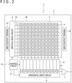
- the semiconductor chip 2 carrying the light detection device 1 has a rectangular-shaped pixel region 2A in the middle of a two-dimensional plane including an X direction and a Y direction intersecting each other, and a peripheral region 2B external to and surrounding the pixel region 2A.
- the pixel region 2A is a light-receiving plane that receives the light focused by the optical system 102 depicted in FIG. 17 , for example.
- a plurality of pixels 3 are arranged in a matrix pattern in the pixel region 2A.
- the pixels 3 are repeatedly arranged in each of the X and Y directions intersecting each other within the two-dimensional plane.
- the X and Y directions are perpendicular to each other, for example.
- the direction perpendicular to both of the X and Y directions is a Z direction (thickness direction).
- a plurality of bonding pads 14 are arranged in the peripheral region 2B.
- the plurality of bonding pads 14 are arranged along each of the four sides of the semiconductor chip 2 on the two-dimensional plane, for example.
- Each of the plurality of bonding pads 14 is an input/output terminal for use in electrically connecting the semiconductor chip 2 to an external device.
- the semiconductor chip 2 has a logic circuit 13 that includes a vertical drive circuit 4, column signal processing circuits 5, a horizontal drive circuit 6, an output circuit 7, and a control circuit 8.
- the logic circuit 13 includes, for example, a CMOS (Complementary MOS) circuit having n-channel conductivity type MOSFETs (Metal Oxide Semiconductor Field Effect Transistors) and p-channel conductivity type MOSFETs as field effect transistors.
- CMOS Complementary MOS
- MOSFETs Metal Oxide Semiconductor Field Effect Transistors
- the vertical drive circuit 4 includes a shift register, for example.
- the vertical drive circuit 4 successively selects desired pixel drive lines 10, and supplies pulses to the selected pixel drive lines 10 for driving relevant pixels 3 so as to drive the pixels 3 in units of rows. That is, the vertical drive circuit 4 selectively scans the pixels 3 in the pixel region 2A in units of rows successively in a vertical direction.
- the vertical drive circuit 4 then supplies the column signal processing circuits 5 via vertical signal lines 11 with the pixel signals that come from the pixels 3 and that are based on signal charges generated by a photoelectric conversion element of each pixel 3 reflecting the quantity of received light.
- the column signal processing circuits 5 are each arranged for each column of the pixels 3, for example. Given signals output from each row of the pixels 3, the column signal processing circuits 5 perform signal processing such as noise removal on the signals output from each pixel column. For example, the column signal processing circuits 5 carry out signal processing such as CDS (Correlated Double Sampling) for removal of fixed pattern noises specific to pixels and AD (Analog Digital) conversion. In an output stage of the column signal processing circuits 5, a horizontal selection switch (not depicted) is provided in such a manner as to be connected to a horizontal signal line 12.
- CDS Correlated Double Sampling
- AD Analog Digital
- the horizontal drive circuit 6 includes a shift register, for example.
- the horizontal drive circuit 6 successively selects each of the column signal processing circuits 5 by consecutively outputting horizontal scanning pulses to the column signal processing circuits 5.
- the horizontal drive circuit 6 then causes each of the column signal processing circuits 5 to output the pixel signal having undergone signal processing, onto the horizontal signal line 12.
- the output circuit 7 Given the pixel signals supplied successively from each column signal processing circuit 5 via the horizontal signal line 12, the output circuit 7 performs signal processing on the supplied pixel signals and outputs the resultant signals.
- the signal processing may include, for example, buffering, black level adjustment, column variation correction, and various types of digital signal processing.
- the control circuit 8 In accordance with a vertical synchronization signal, a horizontal synchronization signal, and a master clock signal, the control circuit 8 generates a clock signal and control signals providing reference to the operation of the vertical drive circuit 4, the column signal processing circuits 5, the horizontal drive circuit 6, and the like. The control circuit 8 then outputs the generated clock signal and control signals to the vertical drive circuit 4, the column signal processing circuits 5, the horizontal drive circuit 6, and the like.
- FIG. 3 is an equivalent circuit diagram depicting a configuration example of a pixel 3.
- the pixel 3 has a photoelectric conversion element PD, a charge accumulation region (Floating Diffusion) FD that accumulates a signal charge resulting from photoelectric conversion by the photoelectric conversion element PD, and a transfer transistor TR that transfers the signal charge resulting from photoelectric conversion by the photoelectric conversion element PD to the charge accumulation region FD.
- the pixel 3 further includes a readout circuit 15 connected electrically to the charge accumulation region FD.
- the photoelectric conversion element PD generates the signal charge reflecting the quantity of received light. Also, the photoelectric conversion element PD temporarily accumulates (holds) the generated signal charge.
- a cathode side of the photoelectric conversion element PD is electrically connected to a source region of the transfer transistor TR.
- An anode side of the photoelectric conversion element PD is electrically connected to a reference potential line (e.g., ground).
- a photodiode may be used as the photoelectric conversion element PD.
- a drain region of the transfer transistor TR is electrically connected to the charge accumulation region FD.
- a gate electrode of the transfer transistor TR is electrically connected to a transfer transistor drive line among the pixel drive lines 10 (see FIG. 2 ).
- the charge accumulation region FD temporarily accumulates and holds the signal charge transferred from the photoelectric conversion element PD via the transfer transistor TR.
- the readout circuit 15 reads the signal charge from the charge accumulation region FD so as to output a pixel signal based on the signal charge.
- the readout circuit 15 includes, but is not limited to, an amplification transistor AMP, a selection transistor SEL, and a reset transistor RST, for example, as pixel transistors.
- These transistors (AMP, SEL, RST) each include, for example, a MOSFET that has a gate insulating film including a silicon oxide film (SiO 2 film), a gate electrode, and a pair of main electrode regions acting as a source region and a drain region.
- These transistors may each alternatively include a MISFET (Metal Insulator Semiconductor FET) of which the gate insulating film is a silicon nitride film (Si 3 N 4 film) or is a multilayer film including a silicon nitride film, a silicon oxide film, and the like.
- MISFET Metal Insulator Semiconductor FET
- a source region of the amplification transistor AMP is electrically connected to a drain region of the selection transistor SEL.
- a drain region of the amplification transistor AMP is electrically connected to a power supply line Vdd and to a drain region of the reset transistor.
- a gate electrode of the amplification transistor AMP is electrically connected to the charge accumulation region FD and to a source region of the reset transistor RST.
- a source region of the selection transistor SEL is electrically connected to a vertical signal line 11 (VSL).
- the drain of the selection transistor SEL is electrically connected to the source region of the amplification transistor AMP.
- a gate electrode of the selection transistor SEL is electrically connected to a selection transistor drive line among the pixel drive lines 10 (see FIG. 2 ).
- the source region of the reset transistor RST is electrically connected to the charge accumulation region FD and to the gate electrode of the amplification transistor AMP.
- the drain region of the reset transistor RST is electrically connected to the power supply line Vdd and to the drain region of the amplification transistor AMP.
- a gate electrode of the reset transistor RST is electrically connected to a reset transistor drive line among the pixel drive lines 10 (see FIG. 2 ).
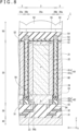
- the light detection device 1 (semiconductor chip 2) has a multilayer structure in which a light collecting layer 50, a semiconductor layer 20, a wiring layer 30, and a support substrate 40 such as a semiconductor substrate are stacked in this order.
- the semiconductor layer 20 includes a semiconductor substrate.
- the semiconductor layer 20 includes, but is not limited to, a monocrystal silicon substrate, for example.
- the semiconductor layer 20 has an element forming surface S1 (the other surface) and a light incident surface S2 (one surface) positioned opposite to each other.
- the element forming surface S1 of the semiconductor layer 20 may be referred to as the principal surface and the light incident surface S2 of the semiconductor layer 20 as the back side.
- the element forming surface S1 is on the side of the wiring layer 30, and the light incident surface S2 is on the side of the light collecting layer 50.
- the semiconductor layer 20 has a photoelectric conversion region 20a formed in each pixel 3. More specifically, in the semiconductor layer 20, island-shaped photoelectric conversion regions 20a partitioned by separation regions 20b are provided in the respective pixels 3, for example.
- the photoelectric conversion regions 20a each include a first region 21, a second region 22, a charge accumulation region 23, a well region, and the like.
- the first region 21 is a first conductivity type semiconductor region such as an n-type semiconductor region (photoelectric conversion part).
- the second region 22 is a second conductivity type semiconductor region such as a p-type semiconductor region.
- the charge accumulation region 23 is a first conductivity type semiconductor region such as an n-type semiconductor region that constitutes the charge accumulation region FD depicted in FIG. 3 .
- the well region is a second conductivity type semiconductor region such as a p-type semiconductor region.
- the photoelectric conversion element PD in FIG. 3 is formed in the photoelectric conversion region 20a.
- the photoelectric conversion region 20a performs photoelectric conversion on the incident light to generate the signal charge.
- Also formed in the semiconductor layer 20 are elements such as the transistors constituting the logic circuit 13 depicted in FIG. 2 and elements such as the transistors in FIG. 3 .
- the example in FIG. 4 indicates the transfer transistor TR formed in the photoelectric conversion region 20a.
- the transfer transistor TR transfers the signal charge generated by photoelectric conversion to the charge accumulation region 23.
- the charge accumulation region 23 accumulates the signal charge.
- the separation regions 20b have a trench structure in which trenches 24 are formed in the semiconductor layer 20 and filled with separation parts 60 or the like, to be discussed later.
- the trenches 24 are positioned in a manner partitioning the photoelectric conversion regions 20a in planar view in the semiconductor layer 20. As depicted in FIG. 4 , the trenches 24 are formed in the separation regions 20b of the semiconductor layer 20, for example. Also, the trenches 24 penetrate the semiconductor layer 20 in the thickness direction thereof. That is, the trenches 24 are formed to provide FTI (Full Trench Isolation).
- FTI Full Trench Isolation
- the light collecting layer 50 includes, but is not limited to, for example, a fixed charge film 51, an insulating film 52, a light blocking layer 53, a planarizing film 54, a color filter 55, and a micro lens (on-chip lens) 56 stacked in this order from the side of the light incident surface S2.
- the fixed charge film 51 is deposited on the semiconductor layer 20 on the side of the light incident surface S2. More specifically, the fixed charge film 51 is deposited in regions including the light incident surface S2 and inner walls of the trenches 24, in a manner covering a surface of the semiconductor layer 20. The fixed charge film 51 is also formed between a first separation part 61 and a second separation part 62, to be discussed later. That is, the fixed charge film 51 is formed at least between the first and second separation parts 61 and 62 to be described below.
- the fixed charge film 51 has a function of capturing electrons and holes that may be generated from the semiconductor layer 20 having defects.
- the fixed charge film 51 includes hafnium oxide (HfO 2 ). Alternatively, zirconium dioxide (ZrO 2 ), tantalum oxide (Ta 2 O 5 ), or the like may be used to form the fixed charge film 51.
- the insulating film 52 is deposited by the CVD method, for example, on that surface of the fixed charge film 51 that is opposite to its surface on the side of the semiconductor layer 20.
- the insulating film 52 is a silicon oxide (SiOz) film, for example.
- the insulating film 52 is deposited in a manner planarizing the trenches 24 by filling them.
- the insulating film 52 deposited in the trenches 24 via the fixed charge film 51 constitutes the first separation part 61, to be discussed below.
- the light blocking layer 53 is stacked on that surface of the insulating film 52 that is opposite to its surface on the side of the fixed charge film 51. More specifically, the light blocking layer 53 is overlaid on the separation regions 20b in planar view. Any suitable light blocking material can be used to form the light blocking layer 53. For example, tungsten (W), aluminum (Al), copper (Cu), or the like can be used.
- the planarizing film 54 is formed in a manner covering that surface of the insulating film 52 that is opposite to its surface on the side of the fixed charge film 51 as well as the light blocking layer 53. Silicon oxide can be used as the material to form the planarizing film 54, for example.
- the micro lens 56 focuses the incident light on the semiconductor layer 20.
- the color filter 55 separates by color the incident light on the semiconductor layer 20.
- the color filter 55 and the micro lens 56 are formed in each of the pixels 3.
- the color filter 55 and the micro lens 56 each include a resinous material, for example.
- the separation parts 60 are formed in the trenches 24 to partition the photoelectric conversion regions 20a.
- the separation parts 60 each include, in the thickness direction of the light detection device 1, the first separation part 61 positioned closer to the side of the light incident surface S2 and the second separation part 62 positioned closer to the side of the element forming surface S1.
- the first separation part 61 is used primarily to partition the photoelectric conversion regions 20a.
- the size of the first separation part 61 in the thickness direction of the semiconductor layer 20 is greater than that of the second separation part 62.
- the second separation part 62 is used not only to partition the photoelectric conversion regions 20a but also to function as a cap on the separation part 60.
- the first separation part 61 serving as a cap, the FTI's shape deformation under the influence of various processes as the transistors, contacts, wires, and the like are being formed on the side of the element forming surface S1 can be suppressed.
- the first separation part 61 is constituted primarily by that portion of the insulating film 52 that is deposited in the trench 24.
- the first separation part 61 includes silicon oxide, for example.
- the second separation part 62 has a first surface S3 on the side of the first separation part 61 and a second surface S4 opposite to the first surface S3.
- the second surface S4 of the second separation part 62 faces the element forming surface S1.
- the first surface S3 is faced with a first material that suppresses etching of the second separation part 62.
- the first surface S3 thus functions as an etching stop surface.
- the second separation part 62 includes the first material.
- the first material is a material resistant to an alkaline etchant such as hydrogen fluoride. Materials of this type include silicon nitride (Si 3 N 4 ), titanium nitride (TiN), and tungsten (W), for example. This embodiment is explained on the assumption that the first material is silicon nitride. It is to be noted that the first material may include impurities.
- a distance “a” between the first surface S3 of the second separation part 62 and the element forming surface S1 is from 200 nm to 300 nm inclusive.
- the distance “a” is greater than a size "b" of the charge accumulation region 23 in the thickness direction.
- the distance between the first surface S3 and the charge accumulation region 23 in the thickness direction is 100 nm. Therefore, there also is a distance of 100 nm between the charge accumulation region 23 on one hand, and the portion of the fixed charge film 51 closest to the element forming surface S1, i.e., the portion between the first surface S3 and the first separation part 61 on the other hand.
- An insulating film 63 covers a side surface (perpendicular to the Z direction) of the second separation part 62.
- the insulating film 63 includes silicon oxide, for example.
- the wiring layer 30 includes an insulating film 31, wiring 32, a gate electrode TRG of the transfer transistor TR, and vias and contacts not depicted.
- the wiring 32 is stacked via the insulating film 31 as illustrated.
- the wiring 32 includes, but not limited to, metal such as copper or aluminum.
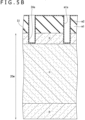
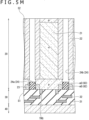
- FIG. 5A a film m1 having openings m1a is formed as a hard mask on the element forming surface S1 of a semiconductor layer 20w.
- the openings m1a are positioned in a manner partitioning the photoelectric conversion regions 20a.
- a known etching technique is used to etch the semiconductor layer 20w from the openings m1a to form trenches 24a.
- the semiconductor layer 20w is thus formed with the trenches 24a in the positions for partitioning the photoelectric conversion regions 20a from the side of the element forming surface S1.
- the film m1 may have a multilayer structure in which a plurality of types of insulating films including silicon oxide and silicon nitride, for example, are stacked.
- the trenches 24a have a depth "c" in the depth direction of the semiconductor layer 20w from the element forming surface S1.
- the region of the semiconductor layer 20w from the element forming surface S1 to the depth "c" is a region where the second region 22 depicted in FIG. 4 is not formed.
- a liner film m2 for protecting side walls of the trenches 24a is stacked on exposed surfaces of the semiconductor layer 20w and the film m1.
- the liner film m2 may have a multilayer structure in which a plurality of types of insulating films including silicon oxide and silicon nitride, for example, are stacked.
- a known etching technique is used to form trenches 24b extending from a bottom of the trenches 24a in the thickness direction of the semiconductor layer 20w.
- the second region 22 is then formed by injecting impurities into exposed surfaces including side walls and a bottom of the trenches 24b.
- the side walls of the trenches 24a are protected by the liner film m2 and thus impervious to the impurities being injected. Thereafter, the liner film m2 is removed.
- the film m1 which is the hard mask, is also partially removed to be made thinner. It is to be noted that, in a case where there is no need to distinguish the trenches 24a and 24b from each other, these trenches are simply referred to as the trenches 24.
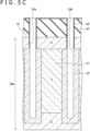
- a film m3 as a silicon oxide film is stacked in a manner covering the exposed surfaces including the side walls and the bottom of the trenches 24.
- a film m4 constituting a sacrificial layer is further stacked. More specifically, the film m4 is stacked in a manner filling the trenches 24.
- the film m4 includes, but is not limited to, a polysilicon (Poly-Si) film, for example.
- a known etch-back technique is used to remove excess portions of the film m4. The portions of the film m4 ranging from the element forming surface S1 to the distance "a" in the thickness direction are removed.
- the portions ranging from the element forming surface S1 to the distance "a" in the thickness direction are thus removed. Further, in the description that follows, the film m4 left intact in the trenches 24 may be referred to as the sacrificial layer M.
- the first material is a material of which the etching rate relative to the selected etchant is lower than that of the material constituting the sacrificial layer M (polysilicon in this embodiment).
- Examples of such a material include silicon nitride (Si 3 N 4 ), titanium nitride (TiN), and tungsten (W). This embodiment is explained on the assumption that the first material is silicon nitride.
- the sacrificial layer M and the film m5 including the first material are stacked in this order in the thickness direction of the semiconductor layer 20w.
- a known etch-back technique, a CMP (Chemical Mechanical Polishing) method, or the like may be used, for example, to planarize the exposed surfaces by removing excess portions of the first material and the film m1 serving as the hard mask. This leaves intact those portions of the film m5 which are embedded in the trenches 24a. More specifically, of the film m5, those portions ranging from the element forming surface S1 to the distance "a" in the thickness direction are left intact. The remaining portions make up the second separation part 62.
- a gate electrode TRG is formed on the element forming surface S1.
- a charge accumulation region 23 is formed in the semiconductor layer 20w by doping with impurities. More specifically, the charge accumulation region 23 is formed by getting the region from the element forming surface S1 to the depth "b" (size "b") in the thickness direction targeted for doping with impurities.
- the wiring layer 30 is formed on the element forming surface S1. The support substrate 40 is further bonded to the wiring layer 30.
- the semiconductor layer 20w on which the wiring layer 30 and the support substrate 40 are formed is turned upside down.
- the CMP method for example, is used to grind that surface of the semiconductor layer 20w that is opposite to the side of the element forming surface S1 so as to make the semiconductor layer 20w thinner. This leaves intact the portions corresponding to the semiconductor layer 20. This also exposes the sacrificial layer M from the side of the light incident surface S2 opposite to the element forming surface S1.
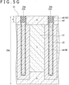
- a film m6 having openings m6a is formed as a hard mask on the light incident surface S2 of the semiconductor layer 20.
- the openings m6a are positioned to overlap with the sacrificial layer M embedded in the trenches 24 in planar view.
- a known etching technique is used to etch the sacrificial layer M via the openings m6a. This removes the sacrificial layer M embedded in the trenches 24.
- the first surface S3 closer to the first separation part 61 functions as an etching stop surface.
- the first material constituting the second separation part 62 and its first surface S3 is a material of which the etching rate relative to the selected etchant is lower than that of the material forming the sacrificial layer M (polysilicon in this embodiment). For this reason, the first surface S3 is hardly or not at all etched. As a result, solely the sacrificial layer M can be removed while the second separation part 62 including the first material is left intact.
- hydrogen fluoride can be used as the etchant but is not limitative.
- the film m6 serving as the hard mask may include silicon oxide, for example. Thereafter, the film m6 as the hard mask is removed.
- excess portions of the film m3, which is a silicon oxide film, are removed. More specifically, of the film m3, the portions except for those covering the side surface (perpendicular to the Z direction) of the second separation part 62 are removed. This can leave intact those portions of the film m3 corresponding to the insulating film 63.
- the fixed charge film 51 and the insulating film 52 are stacked in this order on the exposed surfaces including the side walls of the trenches 24, the first surface S3 of the second separation part 62, and the light incident surface S2.
- Those portions of the insulating film 52 deposited in the trenches 24 via the fixed charge film 51 constitute the first separation part 61. This is how the first separation part 61 is formed.
- the remaining portions of the light collecting layer 50 are formed, which substantially completes the light detection device 1 depicted in FIG. 4 .
- the light detection device 1 is formed in each of a plurality of chip forming regions partitioned by scribe lines (dicing lines) on the semiconductor substrate. Dividing the plurality of chip forming regions along the scribe lines forms semiconductor chips 2 each carrying the light detection device 1.
- the first surface S3 of the second separation part 62 closer to the first separation part 61 is faced with the first material that suppresses etching of the second separation part 62.
- the occurrence of an intense electric field can be suppressed between the fixed charge film 51 and the charge accumulation region 23. Without the intense electric field between the fixed charge film 51 and the charge accumulation region 23, the worsening of white spots and of dark current characteristics can be prevented. With no contact between the fixed charge film 51 and the charge accumulation region 23, an electrical short-circuit therebetween can be prevented. In this manner, it is possible to suppress the worsening of noise characteristics.
- the separation parts 60 including the first separation part 61 and the second separation part 62 formed in the trenches 24 provide the FTI.
- the separation parts 60 on the side of the element forming surface S1 do not constitute an STI (Shallow Trench Isolation) structure.
- the separation parts 60 save space and can be prevented from getting larger in planar view. This can suppress reduction in the degree of freedom in designing the side of the element forming surface S1 even in a case where the photoelectric conversion region 20a is reduced in size by miniaturization.
- the trenches 24 are formed starting from the side of the element forming surface S1. This can improve the overlay accuracy between the trenches 24 and the wiring layer 30 as well as the overlay accuracy between the trenches 24 and the other constituent elements in the semiconductor layer 20 (e.g., charge accumulation region 23). Furthermore, following formation of the wiring layer 30, the material (silicon oxide) constituting the first separation part 61 is embedded into the trenches 24 from the side of the light incident surface S2. Consequently, the material making up the first separation part 61 is not subjected to heat treatment at the time the wiring layer 30 is formed. As a result, warpage and cracking of a wafer can be prevented.
- the first separation part 61 includes silicon oxide. However, this is not limitative of the present technology. As depicted in FIG. 6 , the first separation part 61 may alternatively have a multilayer structure in which a portion 61a including silicon oxide and a portion 61b including metal are stacked in this order, or may have metal alone.
- the metal constituting the portion 61b may be, but is not limited to, aluminum or tungsten, for example.
- the light detection device 1 according to the modification example 1-1 provides advantageous effects similar to those of the light detection device 1 according to the first embodiment discussed above.
- the first separation part 61 includes the portion 61b including metal. This further suppresses color mixing between the photoelectric conversion regions 20a. Moreover, in the case where the first separation part 61 includes metal, the first material of the second separation part provides an advantageous effect of preventing diffusion of the metal.
- the entire second separation part 62 includes the first material.
- the second separation part 62 may alternatively have a multilayer structure in which a first layer 62a including the first material and forming the first surface S3 and a second layer 62b including a second material different from the first material are stacked.
- the second material may include impurities.
- the second material is an insulating material such as silicon oxide.
- the thickness of the first layer 62a in the thickness direction of the semiconductor layer 20 may be between 50 nm and 200 nm inclusive, or between 50 nm and 100 nm inclusive, for example.
- the light detection device 1 according to the modification example 1-2 also provides advantageous effects similar to those of the light detection device 1 according to the first embodiment discussed above.
- the first layer 62a including silicon nitride and the second layer 62b including silicon oxide are stacked. This prevents the positive fixed charge of silicon nitride from affecting the semiconductor layer 20.
- the light detection device 1 according to the modification example 1-3 also provides advantageous effects similar to those of the light detection device 1 according to the first embodiment, the modification example 1-1, and the modification example 1-2 discussed above.
- the second material constituting the second layer 62b depicted in FIG. 7 is an insulating material.
- the second material making up the second layer 62b in FIG. 7 may alternatively be a conductive material such as polysilicon or tungsten.
- the light detection device 1 according to the modification example 1-4 also provides advantageous effects similar to those of the light detection device 1 according to the first embodiment discussed above.
- the second separation part 62 can be used as an electrode. This improves the degree of freedom in design.
- the second material constituting the second layer 62b depicted in FIG. 8 is an insulating material.
- the second material forming the second layer 62b in FIG. 8 may alternatively be a conductive material such as polysilicon, for example.
- the light detection device 1 according to the modification example 1-5 also provides advantageous effects similar to those of the light detection device 1 according to the first embodiment discussed above.
- the second separation part 62 may be used as an electrode. This improves the degree of freedom in design.
- the light detection device 1 according to the second embodiment differs from the light detection device 1 according to the first embodiment above in that a second separation part 62A is provided in place of the second separation part 62.
- the remaining configuration of the light detection device 1 is basically similar to the configuration of the light detection device 1 according to the first embodiment discussed above.
- the constituent elements explained already are designated by the same reference signs and will not be discussed further.
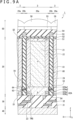
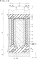
- the separation parts 60 each include the first separation part 61 positioned closer to the side of the light incident surface S2 and the second separation part 62A positioned closer to the side of the element forming surface S1 in the thickness direction of the light detection device 1.
- the second separation part 62A has a multilayer structure in which a first layer 62Aa including the first material and constituting the first surface S3 and a second layer 62Ab including the second material different from the first material are stacked. Also, the separation parts 60 each have an insulating film 64 that separates the second separation part 62A and the first separation part 61 from each other or, to be more specific, separates the second separation part 62A and the fixed charge film 51 from each other.
- the first layer 62Aa has, more specifically, a facing part 62Aa1 and a side wall part 62Aa2, the facing part 62Aa1 facing the first separation part 61 and constituting the first surface S3, the side wall part 62Aa2 being positioned between the semiconductor layer 20 and the insulating film 64 (between a side surface of the second layer 62Ab and the insulating film 63).
- the second material constituting the second layer 62Ab is an insulating material such as silicon oxide.
- the second separation part 62A has the first surface S3 closer to the first separation part 61 and the second surface S4 opposite to the side of the first surface S3.
- the first surface S3 functions as an etching stop surface.
- the second surface S4 of the second separation part 62A faces the element forming surface S1.
- the first material may be, but is not limited to, silicon nitride, for example. Further, the first material is a material of which the etching rate relative to the selected etchant is lower than that of the material constituting the sacrificial layer M explained above in connection with the manufacturing method. For this reason, the first material need only be determined according to the material making up the sacrificial layer M.
- the first material may thus be something other than silicon nitride. For example, any one of polysilicon, silicon oxide, hafnium oxide (HfO 2 ), and aluminum oxide (Al 2 O 3 ) may be selected as the first material, according to the material constituting the sacrificial layer M.
- the thickness of the facing part 62Aa1 in the thickness direction of the semiconductor layer 20 (the thickness of the first layer 62Aa in the stacking direction) is between 5 nm and 50 nm inclusive or between 10 nm and 50 nm inclusive.
- the insulating film 64 is provided to suppress the influence of the positive fixed charge borne by silicon nitride.
- the insulating film 64 is a silicon oxide film, for example.
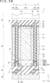
- the insulating film 64 has a thickness between 10 nm and 20 nm inclusive, for example, but is not limited thereto. There may be cases where the influence of the positive fixed charge borne by silicon nitride can be suppressed depending on design, without recourse to the insulating film 64, as depicted in FIG. 9B . Further, the insulating film 64 may be given a thickness of 40 nm or less at the time of manufacture in consideration of etchant penetration from the side of the light incident surface S2.
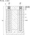
- a method of manufacturing the light detection device 1 is explained below with reference to FIGS. 10A through 10C . It is to be noted that what is described below are primarily the processes of forming the separation parts 60. For this reason, those constituent elements of the light detection device 1 which can be formed by known methods may be omitted from the explanation of the forming processes. Also, the processes similar to those of the method of manufacturing the light detection device 1 according to the above-described first embodiment of the present technology will not be discussed further.
- a known deposition technique or the like is used to form the insulating film 64, thereby obtaining the state illustrated in FIG. 10A .
- a film m5Aa including the first material is stacked in a manner covering the exposed surfaces including the side walls and the bottom of the trenches 24a.
- a film m5Ab including the second material is further stacked in a manner filling the trenches 24a.
- a known etch-back technique the CMP (Chemical Mechanical Polishing) method, or the like may be used, for example, to planarize the exposed surfaces by removing excess portions of the first and second materials as well as the film m1 serving as the hard mask. This leaves intact those portions of the films m5Aa and m5Ab which are embedded in the trenches 24a. The remaining portions make up the first layer 62Aa and the second layer 62Ab of the second separation part 62A.
- the subsequent manufacturing processes are similar to those explained above in connection with the first embodiment and thus will not be discussed further.
- the thickness of the first layer 62Aa in the stacking direction is less than in the case of the first embodiment. This further suppresses the influence of silicon nitride on the semiconductor layer 20.
- the first layer 62Aa has both the facing part 62Aa1 and the side wall part 62Aa2. This means that, even when the thickness of the first layer 62Aa in the stacking direction is less than in the case of the first embodiment, the etchant used to remove the sacrificial layer M is prevented from reaching the second layer 62Ab inside the first layer 62Aa. This prevents the second separation part 62A from being etched.
- the insulating film 64 formed in the process depicted in FIG. 10A may be formed following removal of the sacrificial layer M.
- the first separation part 61 includes silicon oxide. However, this is not limitative of the present technology. As depicted in FIG. 11 , the first separation part 61 may alternatively have a multilayer structure in which the portion 61a including silicon oxide and the portion 61b including metal are stacked in this order.
- the metal making up the portion 61b may be, but is not limited to, aluminum or tungsten, for example.
- the light detection device 1 according to the modification example 2-1 also provides advantageous effects similar to those of the light detection device 1 according to the second embodiment discussed above.
- the first separation part 61 has the portion 61b including metal. This makes it possible further to suppress color mixing between the photoelectric conversion regions 20a.
- the facing part 62Aa1 forms the first surface S3. This makes it possible to prevent the second separation part 62A from being etched upon removal of the sacrificial layer M.
- the second separation part 62A may provide the STI (Shallow Trench Isolation). More specifically, the second separation part 62A may have a horizontal size greater than that of the first separation part 61.
- the second separation part 62A has a multilayer structure in which a first layer 62Ac including the first material and forming the first surface S3 and a second layer 62Ad including the second material different from the first material are stacked. The first layer 62Ac is formed in a region where there is an overlap at least with the first separation part 61 in the thickness direction (i.e., an overlap in planar view).
- the light detection device 1 according to the modification example 2-3 also provides advantageous effects similar to those of the light detection device 1 according to the second embodiment discussed above.
- the second material making up the second layer 62Ab or 62Ad in FIGS. 9A , 11 , and 12 is an insulating material.
- the second material may be a conductive material such as polysilicon.
- the light detection device 1 according to the modification example 2-4 also provides advantageous effects similar to those of the light detection device 1 according to the second embodiment discussed above.
- the second separation part 62A may be used as an electrode. This improves the degree of freedom in design.
- the light detection device 1 according to the third embodiment differs from the light detection device 1 according to the first embodiment above in that a second separation part 62B is provided in place of the second separation part 62.
- the remaining configuration of the light detection device 1 is basically similar to the configuration of the light detection device 1 according to the first embodiment discussed above.
- the constituent elements explained already are designated by the same reference signs and will not be discussed further.
- the separation parts 60 each include the first separation part 61 positioned closer to the side of the light incident surface S2 and the second separation part 62B positioned closer to the side of the element forming surface S1 in the thickness direction of the light detection device 1.
- the trenches 24 in which the separation parts 60 are formed include a first trench 24c positioned closer to the side of the element forming surface S1 and constituting the STI and a second trench 24d positioned closer to the side of the light incident surface S2 and constituting the FTI. It is to be noted that, in the case where the first trench 24c and the second trench 24d are not distinguished from each other, they are simply referred to as the trenches 24.
- the second separation part 62B is provided in a region ranging from the first trench 24c to a portion of the second trench 24d. Further, the second separation part 62B has a multilayer structure in which a first layer 62Ba including the first material and constituting the first surface S3 and a second layer 62Bb including the second material different from the first material are stacked.
- the first layer 62Ba is formed in a portion of the second trench 24d. More specifically, the first layer 62Ba is provided in a portion closer to the first trench 24c inside the second trench 24d.
- the second layer 62Bb is formed in the first trench 24c constituting the STI.
- the first layer 62Ba has a horizontal size equal to that of the first separation part 61
- the second layer 62Bb has a horizontal size greater than that of the first separation part 61.
- the second separation part 62B has the first surface S3 closer to the above-mentioned first separation part 61 and the second surface S4 opposite to the side of the first surface S3.
- the first surface S3 functions as an etching stop surface.
- the second surface S4 of the second separation part 62B (second layer 62Bb) faces the element forming surface S1.
- the first material is silicon doped with impurities. More specifically, the first material may be, but is not limited to, polysilicon doped with impurities, for example.
- the impurities may be boron (B), for example, but are not limited thereto.
- the concentration of boron in the first material is 5 ⁇ 10 18 atoms/cm 3 or higher.
- the second material is an insulating material such as silicon oxide, for example, but is not limited thereto.
- a method of manufacturing the light detection device 1 is explained below with reference to FIGS. 14A through 14G . It is to be noted that what is described below are primarily the processes of forming the separation parts 60. For this reason, those constituent elements of the light detection device 1 which can be formed by known methods may be omitted from the explanation of the forming processes. Also, the processes similar to those of the method of manufacturing the light detection device 1 according to the above-described first embodiment of the present technology will not be discussed further.
- the first trench 24c constituting the STI and the second trench 24d constituting the FTI are formed in the semiconductor layer 20w.
- the film m3 including silicon oxide is stacked in a manner covering the exposed surfaces including the side walls and the bottom of the trenches 24.
- the film m4 forming a sacrificial layer is stacked in the trenches 24.
- the sacrificial layer includes polysilicon, for example.
- a known etch-back technique is used to remove the film m4 stacked in the first trench 24c.
- impurities are injected near the exposed surface of the film m4 including polysilicon and remaining in the trenches 24.
- boron is injected.
- the first material is thus obtained by injecting boron into the polysilicon.
- the region doped with the impurities forms the first layer 62Ba, and the remaining portions make up the sacrificial layer M.
- a film m7 including silicon oxide is stacked in a manner filling the inside of the first trench 24c. Thereafter, an excess insulating film on the side of the element forming surface S1 is removed, and the processes explained in conjunction with the first embodiment and depicted in FIGS. 5H and 5I are carried out.
- the semiconductor layer 20w having the wiring layer 30 and the support substrate 40 formed therein is turned upside down as depicted in FIG. 14F .
- the semiconductor layer 20w is made thinner from the surface opposite to the side of the element forming surface S1 in order to expose the sacrificial layer M stacked inside the second trench 24d.
- the first surface S3 functions as an etching stop surface. More specifically, the first material (polysilicon doped with boron) constituting the first layer 62Ba and its first surface S3 is a material of which the etching rate relative to the selected etchant is lower than that of the material forming the sacrificial layer M (polysilicon in this embodiment). Consequently, the first surface S3 is hardly or not at all etched.
- the sacrificial layer M can be removed while the first layer 62Ba including the first material is left intact.
- hydrogen fluoride can be used as the etchant but is not limitative. The subsequent processes are similar to those explained above in connection with the first embodiment and thus will not be discussed further.
- the light detection device 1 according to the third embodiment also provides advantageous effects similar to those of the light detection device 1 according to the first embodiment discussed above.
- the first material constituting the second separation part 62B is doped with boron.
- the first material may be doped with boron and carbon (C).
- boron and carbon are injected into the film m4 including polysilicon. Carbon is injected to control the diffusion of boron.
- the light detection device 1 according to the modification example 3-1 also provides advantageous effects similar to those of the light detection device 1 according to the third embodiment discussed above.
- the first material is formed by injection of boron after the film m4 including polysilicon is etched back.
- a film m8 including the first material may be stacked by forming a silicon film (e.g., polysilicon film) through the mixture of impurities after the film m4 is etched back, as depicted in FIG. 15 . Thereafter, excess portions of the film m8 are etched back to leave intact the portions corresponding to the first layer 62Ba.
- the light detection device 1 according to the modification example 3-2 also provides advantageous effects similar to those of the light detection device 1 according to the third embodiment discussed above.
- the first separation part 61 includes silicon oxide. However, this is not limitative of the present technology. As depicted in FIG 16 , the first separation part 61 may alternatively have a multilayer structure in which the portion 61a including silicon oxide and the portion 61b including metal are stacked in this order.
- the metal constituting the portion 61b may be metal such as aluminum or tungsten, for example, but is not limited thereto.
- the light detection device 1 according to the modification example 3-3 also provides advantageous effects similar to those of the light detection device 1 according to the third embodiment discussed above.
- the first separation part 61 in the light detection device 1 according to the modification example 3-3 has the portion 61b including metal, it is possible further to suppress color mixing between the photoelectric conversion regions 20a.
- the separation parts 60 have both the portions constituting the FTI and the portions constituting the STI. However, this is not limitative of the present technology. Alternatively, the separation parts 60 may only have the portions constituting the FTI.
- the light detection device 1 according to the modification example 3-4 also provides advantageous effects similar to those of the light detection device 1 according to the third embodiment discussed above.
- the electronic equipment 100 includes a solid-state imaging device 101, an optical lens 102, a shutter device 103, a drive circuit 104, and a signal processing circuit 105.
- the electronic equipment 100 may be electronic equipment such as a camera, but is not limited thereto.
- the electronic equipment 100 has the light detection device 1 as the solid-state imaging device 101.
- the solid-state imaging device 101 has the first surface S3 of the second separation part 62 faced with the first material that suppresses the etching of the second separation part 62, the first surface S3 being positioned closer to the first separation part 61. This makes it possible to suppress the worsening of noise characteristics.
- the electronic equipment 100 is not limited to the camera and may be any other electric devices.
- the electronic equipment 100 may be an imaging device such as a camera module for mobile devices such as mobile phones.
- the electronic equipment 100 can have, as the solid-state imaging device 101, the light detection device 1 according to any one of the first through third embodiments and their modification examples, or the light detection device 1 according to a combination of at least two of the first through third embodiments and their modification examples.
- FIG. 18 is a block diagram depicting an example of schematic configuration of a vehicle control system as an example of a mobile body control system to which the technology according to an embodiment of the present disclosure can be applied.
- the vehicle control system 12000 includes a plurality of electronic control units connected to each other via a communication network 12001.
- the vehicle control system 12000 includes a driving system control unit 12010, a body system control unit 12020, an outside-vehicle information detecting unit 12030, an in-vehicle information detecting unit 12040, and an integrated control unit 12050.
- a microcomputer 12051, a sound/image output section 12052, and a vehicle-mounted network interface (I/F) 12053 are illustrated as a functional configuration of the integrated control unit 12050.
- the microcomputer 12051 can calculate a control target value for the driving force generating device, the steering mechanism, or the braking device on the basis of the information about the inside or outside of the vehicle which information is obtained by the outside-vehicle information detecting unit 12030 or the in-vehicle information detecting unit 12040, and output a control command to the driving system control unit 12010.
- the microcomputer 12051 can perform cooperative control intended to implement functions of an advanced driver assistance system (ADAS) which functions include collision avoidance or shock mitigation for the vehicle, following driving based on a following distance, vehicle speed maintaining driving, a warning of collision of the vehicle, a warning of deviation of the vehicle from a lane, or the like.
- ADAS advanced driver assistance system
- the microcomputer 12051 can perform cooperative control intended for automated driving, which makes the vehicle to travel automatedly without depending on the operation of the driver, or the like, by controlling the driving force generating device, the steering mechanism, the braking device, or the like on the basis of the information about the outside or inside of the vehicle which information is obtained by the outside-vehicle information detecting unit 12030 or the in-vehicle information detecting unit 12040.
- the microcomputer 12051 can output a control command to the body system control unit 12020 on the basis of the information about the outside of the vehicle which information is obtained by the outside-vehicle information detecting unit 12030.
- the microcomputer 12051 can perform cooperative control intended to prevent a glare by controlling the headlamp so as to change from a high beam to a low beam, for example, in accordance with the position of a preceding vehicle or an oncoming vehicle detected by the outside-vehicle information detecting unit 12030.
- FIG. 19 is a diagram depicting an example of the installation position of the imaging section 12031.
- the imaging section 12031 includes imaging sections 12101, 12102, 12103, 12104, and 12105.
- At least one of the imaging sections 12101 to 12104 may have a function of obtaining distance information.
- at least one of the imaging sections 12101 to 12104 may be a stereo camera constituted of a plurality of imaging elements, or may be an imaging element having pixels for phase difference detection.
- the microcomputer 12051 can determine a distance to each three-dimensional object within the imaging ranges 12111 to 12114 and a temporal change in the distance (relative speed with respect to the vehicle 12100) on the basis of the distance information obtained from the imaging sections 12101 to 12104, and thereby extract, as a preceding vehicle, a nearest three-dimensional object in particular that is present on a traveling path of the vehicle 12100 and which travels in substantially the same direction as the vehicle 12100 at a predetermined speed (for example, equal to or more than 0 km/hour). Further, the microcomputer 12051 can set a following distance to be maintained in front of a preceding vehicle in advance, and perform automatic brake control (including following stop control), automatic acceleration control (including following start control), or the like. It is thus possible to perform cooperative control intended for automated driving that makes the vehicle travel automatedly without depending on the operation of the driver or the like.
- automatic brake control including following stop control
- automatic acceleration control including following start control
- the microcomputer 12051 can classify three-dimensional object data on three-dimensional objects into three-dimensional object data of a two-wheeled vehicle, a standard-sized vehicle, a large-sized vehicle, a pedestrian, a utility pole, and other three-dimensional objects on the basis of the distance information obtained from the imaging sections 12101 to 12104, extract the classified three-dimensional object data, and use the extracted three-dimensional object data for automatic avoidance of an obstacle.
- the microcomputer 12051 identifies obstacles around the vehicle 12100 as obstacles that the driver of the vehicle 12100 can recognize visually and obstacles that are difficult for the driver of the vehicle 12100 to recognize visually. Then, the microcomputer 12051 determines a collision risk indicating a risk of collision with each obstacle.
- the microcomputer 12051 In a situation in which the collision risk is equal to or higher than a set value and there is thus a possibility of collision, the microcomputer 12051 outputs a warning to the driver via the audio speaker 12061 or the display section 12062, and performs forced deceleration or avoidance steering via the driving system control unit 12010. The microcomputer 12051 can thereby assist in driving to avoid collision.
- the sound/image output section 12052 controls the display section 12062 so that a square contour line for emphasis is displayed so as to be superimposed on the recognized pedestrian.
- the sound/image output section 12052 may also control the display section 12062 so that an icon or the like representing the pedestrian is displayed at a desired position.
- the technology according to the present disclosure can be applied to the imaging section 12031 or the like from among the components discussed above.
- the light detection device 1 depicted in FIG. 4 and other figures can be adopted as the imaging section 12031.
- Applying the technology according to the present disclosure to the imaging section 12031 can suppress the worsening of noise characteristics and thereby provide easier-to-view captured images. This in turn helps alleviate the fatigue of the driver.
- FIG. 20 is a view depicting an example of a schematic configuration of an endoscopic surgery system to which the technology according to an embodiment of the present disclosure (present technology) can be applied.
- FIG. 20 a state is illustrated in which a surgeon (medical doctor) 11131 is using an endoscopic surgery system 11000 to perform surgery for a patient 11132 on a patient bed 11133.
- the endoscopic surgery system 11000 includes an endoscope 11100, other surgical tools 11110 such as a pneumoperitoneum tube 11111 and an energy device 11112, a supporting arm apparatus 11120 which supports the endoscope 11100 thereon, and a cart 11200 on which various apparatus for endoscopic surgery are mounted.
- the lens barrel 11101 has, at a distal end thereof, an opening in which an objective lens is fitted.
- a light source apparatus 11203 is connected to the endoscope 11100 such that light generated by the light source apparatus 11203 is introduced to a distal end of the lens barrel 11101 by a light guide extending in the inside of the lens barrel 11101 and is irradiated toward an observation target in a body cavity of the patient 11132 through the objective lens.
- the endoscope 11100 may be a forward-viewing endoscope or may be an oblique-viewing endoscope or a side-viewing endoscope.
- An optical system and an image pickup element are provided in the inside of the camera head 11102 such that reflected light (observation light) from the observation target is condensed on the image pickup element by the optical system.
- the observation light is photo-electrically converted by the image pickup element to generate an electric signal corresponding to the observation light, namely, an image signal corresponding to an observation image.
- the image signal is transmitted as RAW data to a CCU 11201.
- the display apparatus 11202 displays thereon an image based on an image signal, for which the image processes have been performed by the CCU 11201, under the control of the CCU 11201.
- the light source apparatus 11203 includes a light source such as, for example, a light emitting diode (LED) and supplies irradiation light upon imaging of a surgical region to the endoscope 11100.
- a light source such as, for example, a light emitting diode (LED) and supplies irradiation light upon imaging of a surgical region to the endoscope 11100.
- LED light emitting diode
- An inputting apparatus 11204 is an input interface for the endoscopic surgery system 11000.
- a user can perform inputting of various kinds of information or instruction inputting to the endoscopic surgery system 11000 through the inputting apparatus 11204.
- the user would input an instruction or a like to change an image pickup condition (type of irradiation light, magnification, focal distance or the like) by the endoscope 11100.
- the light source apparatus 11203 which supplies irradiation light when a surgical region is to be imaged to the endoscope 11100 may include a white light source which includes, for example, an LED, a laser light source or a combination of them.
- a white light source includes a combination of red, green, and blue (RGB) laser light sources, since the output intensity and the output timing can be controlled with a high degree of accuracy for each color (each wavelength), adjustment of the white balance of a picked up image can be performed by the light source apparatus 11203.
- RGB red, green, and blue
- the light source apparatus 11203 may be controlled such that the intensity of light to be outputted is changed for each predetermined time.
- driving of the image pickup element of the camera head 11102 in synchronism with the timing of the change of the intensity of light to acquire images time-divisionally and synthesizing the images an image of a high dynamic range free from underexposed blocked up shadows and overexposed highlights can be created.
- the light source apparatus 11203 may be configured to supply light of a predetermined wavelength band ready for special light observation.
- special light observation for example, by utilizing the wavelength dependency of absorption of light in a body tissue to irradiate light of a narrow band in comparison with irradiation light upon ordinary observation (namely, white light), narrow band observation (narrow band imaging) of imaging a predetermined tissue such as a blood vessel of a superficial portion of the mucous membrane or the like in a high contrast is performed.
- fluorescent observation for obtaining an image from fluorescent light generated by irradiation of excitation light may be performed.
- FIG. 21 is a block diagram depicting an example of a functional configuration of the camera head 11102 and the CCU 11201 depicted in FIG. 20 .
- the lens unit 11401 is an optical system, provided at a connecting location to the lens barrel 11101. Observation light taken in from a distal end of the lens barrel 11101 is guided to the camera head 11102 and introduced into the lens unit 11401.
- the lens unit 11401 includes a combination of a plurality of lenses including a zoom lens and a focusing lens.
- the number of image pickup elements which is included by the image pickup unit 11402 may be one (single-plate type) or a plural number (multi-plate type). Where the image pickup unit 11402 is configured as that of the multi-plate type, for example, image signals corresponding to respective R, G and B are generated by the image pickup elements, and the image signals may be synthesized to obtain a color image.
- the image pickup unit 11402 may also be configured so as to have a pair of image pickup elements for acquiring respective image signals for the right eye and the left eye ready for three dimensional (3D) display. If 3D display is performed, then the depth of a living body tissue in a surgical region can be comprehended more accurately by the surgeon 11131. It is to be noted that, where the image pickup unit 11402 is configured as that of stereoscopic type, a plurality of systems of lens units 11401 are provided corresponding to the individual image pickup elements.
- the image pickup unit 11402 may not necessarily be provided on the camera head 11102.
- the image pickup unit 11402 may be provided immediately behind the objective lens in the inside of the lens barrel 11101.
- the driving unit 11403 includes an actuator and moves the zoom lens and the focusing lens of the lens unit 11401 by a predetermined distance along an optical axis under the control of the camera head controlling unit 11405. Consequently, the magnification and the focal point of a picked up image by the image pickup unit 11402 can be adjusted suitably.
- the communication unit 11404 includes a communication apparatus for transmitting and receiving various kinds of information to and from the CCU 11201.
- the communication unit 11404 transmits an image signal acquired from the image pickup unit 11402 as RAW data to the CCU 11201 through the transmission cable 11400.
- the communication unit 11404 receives a control signal for controlling driving of the camera head 11102 from the CCU 11201 and supplies the control signal to the camera head controlling unit 11405.
- the control signal includes information relating to image pickup conditions such as, for example, information that a frame rate of a picked up image is designated, information that an exposure value upon image picking up is designated and/or information that a magnification and a focal point of a picked up image are designated.
- the image pickup conditions such as the frame rate, exposure value, magnification or focal point may be designated by the user or may be set automatically by the control unit 11413 of the CCU 11201 on the basis of an acquired image signal.
- an auto exposure (AE) function, an auto focus (AF) function and an auto white balance (AWB) function are incorporated in the endoscope 11100.
- the camera head controlling unit 11405 controls driving of the camera head 11102 on the basis of a control signal from the CCU 11201 received through the communication unit 11404.
- the communication unit 11411 includes a communication apparatus for transmitting and receiving various kinds of information to and from the camera head 11102.
- the communication unit 11411 receives an image signal transmitted thereto from the camera head 11102 through the transmission cable 11400.
- the communication unit 11411 transmits a control signal for controlling driving of the camera head 11102 to the camera head 11102.
- the image signal and the control signal can be transmitted by electrical communication, optical communication or the like.
- the image processing unit 11412 performs various image processes for an image signal in the form of RAW data transmitted thereto from the camera head 11102.
- the control unit 11413 performs various kinds of control relating to image picking up of a surgical region or the like by the endoscope 11100 and display of a picked up image obtained by image picking up of the surgical region or the like. For example, the control unit 11413 creates a control signal for controlling driving of the camera head 11102.
- control unit 11413 controls, on the basis of an image signal for which image processes have been performed by the image processing unit 11412, the display apparatus 11202 to display a picked up image in which the surgical region or the like is imaged.
- control unit 11413 may recognize various objects in the picked up image using various image recognition technologies.
- the control unit 11413 can recognize a surgical tool such as forceps, a particular living body region, bleeding, mist when the energy device 11112 is used and so forth by detecting the shape, color and so forth of edges of objects included in a picked up image.
- the control unit 11413 may cause, when it controls the display apparatus 11202 to display a picked up image, various kinds of surgery supporting information to be displayed in an overlapping manner with an image of the surgical region using a result of the recognition. Where surgery supporting information is displayed in an overlapping manner and presented to the surgeon 11131, the burden on the surgeon 11131 can be reduced and the surgeon 11131 can proceed with the surgery with certainty.
- the transmission cable 11400 which connects the camera head 11102 and the CCU 11201 to each other is an electric signal cable ready for communication of an electric signal, an optical fiber ready for optical communication or a composite cable ready for both of electrical and optical communications.
- communication is performed by wired communication using the transmission cable 11400
- the communication between the camera head 11102 and the CCU 11201 may be performed by wireless communication.
- the technology according to the present disclosure can be applied to the image pickup unit 11402 of the camera head 11102 from among the components discussed above.
- the light detection device 1 depicted in FIG. 4 and other figures can be adopted as the image pickup unit 10402.
- Applying the technology according to the present disclosure to the camera head 11102 can suppress the worsening of noise characteristics and thereby provide clearer images of the surgical region. This in turn allows the surgeon to reliably verify the surgical region.
- the technical ideas explained above in connection with the first through fourth embodiments may be combined as desired.
- the first material making up the second separation part 62B in the light detection device 1 according to the third embodiment above is silicon doped with impurities, such a technical idea may also be applied to the light detection device 1 described in the first and second embodiments.
- the first material is any one of polysilicon, silicon oxide, hafnium oxide, and aluminum oxide, such a technical idea may also be applied to the first material of the first embodiment.
- the light detection device 1 according to the second embodiment above has the insulating film 64 separating the second separation part 62A from the fixed charge film 51
- such a technical idea may also be applied to the light detection device 1 described in the first and third embodiments. In this manner, the embodiments and their variations may be diversely combined in accordance with each of the technical ideas.
- the present technology can be applied not only to the above-described solid-state imaging device as the image sensor but also to a whole range of light detection devices including distance measuring sensors also called ToF (Time of Flight) sensors that measure distances.
- the distance measuring sensor is a sensor that emits irradiation light to an object, detects reflected light from a surface of the object, and calculates the distance to the object based on the time of flight of the irradiation light from its emission to its return as reflected light.
- the structure of the above-described separation parts 60 can be adopted as the structure of the distance measuring sensor.
- the separation parts 60 may partition these photoelectric conversion elements PD configured in the one photoelectric conversion region 20a.
- the light detection device 1 may be a multilayer CIS (CMOS Image Sensor) in which two or more semiconductor substrates are stacked one on top of another.
- CMOS Image Sensor CMOS Image Sensor
- at least either the logic circuit 13 or the readout circuit 15 may be mounted on a semiconductor substrate different from the one on which the photoelectric conversion regions 20a are formed.
Landscapes
- Solid State Image Pick-Up Elements (AREA)
- Light Receiving Elements (AREA)
Applications Claiming Priority (2)
| Application Number | Priority Date | Filing Date | Title |
|---|---|---|---|
| JP2021151390 | 2021-09-16 | ||
| PCT/JP2022/014483 WO2023042462A1 (ja) | 2021-09-16 | 2022-03-25 | 光検出装置、光検出装置の製造方法、及び電子機器 |
Publications (1)
| Publication Number | Publication Date |
|---|---|
| EP4404250A1 true EP4404250A1 (en) | 2024-07-24 |
Family
ID=85601956
Family Applications (1)
| Application Number | Title | Priority Date | Filing Date |
|---|---|---|---|
| EP22869614.2A Withdrawn EP4404250A1 (en) | 2021-09-16 | 2022-03-25 | Light detecting device, method for manufacturing light detecting device, and electronic instrument |
Country Status (8)
| Country | Link |
|---|---|
| US (1) | US20240379709A1 (https=) |
| EP (1) | EP4404250A1 (https=) |
| JP (1) | JPWO2023042462A1 (https=) |
| KR (1) | KR20240058850A (https=) |
| CN (1) | CN117716504A (https=) |
| DE (1) | DE112022004422T5 (https=) |
| TW (1) | TW202322373A (https=) |
| WO (1) | WO2023042462A1 (https=) |
Families Citing this family (5)
| Publication number | Priority date | Publication date | Assignee | Title |
|---|---|---|---|---|
| WO2024202548A1 (ja) * | 2023-03-29 | 2024-10-03 | ソニーセミコンダクタソリューションズ株式会社 | 光検出装置及び電子機器 |
| CN121400092A (zh) * | 2023-07-28 | 2026-01-23 | 索尼半导体解决方案公司 | 光检测装置和电子设备 |
| US20250072148A1 (en) * | 2023-08-23 | 2025-02-27 | Taiwan Semiconductor Manufacturing Company, Ltd. | Deep trench isolation structure for image sensor |
| US20250120209A1 (en) * | 2023-10-04 | 2025-04-10 | Taiwan Semiconductor Manufacturing Company, Ltd. | Image sensor device and method of manufacturing the same |
| WO2025225733A1 (ja) * | 2024-04-26 | 2025-10-30 | ソニーセミコンダクタソリューションズ株式会社 | 光検出装置及び電子機器 |
Family Cites Families (7)
| Publication number | Priority date | Publication date | Assignee | Title |
|---|---|---|---|---|
| JP2011054741A (ja) * | 2009-09-01 | 2011-03-17 | Toshiba Corp | 裏面照射型固体撮像装置 |
| JP6299058B2 (ja) * | 2011-03-02 | 2018-03-28 | ソニー株式会社 | 固体撮像装置、固体撮像装置の製造方法及び電子機器 |
| KR102209097B1 (ko) * | 2014-02-27 | 2021-01-28 | 삼성전자주식회사 | 이미지 센서 및 이의 제조 방법 |
| KR102268714B1 (ko) * | 2014-06-23 | 2021-06-28 | 삼성전자주식회사 | 이미지 센서 및 이의 제조 방법 |
| KR102551489B1 (ko) * | 2017-10-13 | 2023-07-04 | 삼성전자주식회사 | 이미지 센서 |
| EP3709357A4 (en) | 2017-11-09 | 2020-12-23 | Sony Semiconductor Solutions Corporation | IMAGE CAPTURE ELEMENT AND ELECTRONIC DEVICE |
| JP7250427B2 (ja) * | 2018-02-09 | 2023-04-03 | キヤノン株式会社 | 光電変換装置、撮像システム、および移動体 |
-
2022
- 2022-03-25 DE DE112022004422.5T patent/DE112022004422T5/de active Pending
- 2022-03-25 EP EP22869614.2A patent/EP4404250A1/en not_active Withdrawn
- 2022-03-25 WO PCT/JP2022/014483 patent/WO2023042462A1/ja not_active Ceased
- 2022-03-25 KR KR1020247006556A patent/KR20240058850A/ko not_active Withdrawn
- 2022-03-25 CN CN202280052277.1A patent/CN117716504A/zh active Pending
- 2022-03-25 US US18/690,173 patent/US20240379709A1/en active Pending
- 2022-03-25 JP JP2023548116A patent/JPWO2023042462A1/ja not_active Abandoned
- 2022-08-19 TW TW111131268A patent/TW202322373A/zh unknown
Also Published As
| Publication number | Publication date |
|---|---|
| WO2023042462A1 (ja) | 2023-03-23 |
| CN117716504A (zh) | 2024-03-15 |
| JPWO2023042462A1 (https=) | 2023-03-23 |
| DE112022004422T5 (de) | 2024-07-11 |
| US20240379709A1 (en) | 2024-11-14 |
| TW202322373A (zh) | 2023-06-01 |
| KR20240058850A (ko) | 2024-05-03 |
Similar Documents
| Publication | Publication Date | Title |
|---|---|---|
| US12211875B2 (en) | Imaging element having p-type and n-type solid phase diffusion layers formed in a side wall of an interpixel light shielding wall | |
| US20240266381A1 (en) | Imaging element and semiconductor element | |
| EP4404250A1 (en) | Light detecting device, method for manufacturing light detecting device, and electronic instrument | |
| US20240431128A1 (en) | Solid-state imaging element, electronic device, and manufacturing method of solid-state imaging element | |
| EP4131429A1 (en) | Imaging device and electronic apparatus | |
| US12615454B2 (en) | Imaging element and imaging device | |
| US20240088191A1 (en) | Photoelectric conversion device and electronic apparatus | |
| US20220344390A1 (en) | Organic cis image sensor | |
| US11502122B2 (en) | Imaging element and electronic device | |
| US20200286936A1 (en) | Semiconductor device and manufacturing method of semiconductor device | |
| WO2024142627A1 (en) | Photodetector and electronic apparatus | |
| US20250228020A1 (en) | Photodetector and electronic apparatus | |
| US20250194283A1 (en) | Photodetection device and electronic apparatus | |
| WO2017122537A1 (ja) | 受光素子、受光素子の製造方法、撮像素子および電子機器 | |
| US20250133845A1 (en) | Photodetector and electronic apparatus | |
| EP4386847A1 (en) | Imaging device and electronic apparatus | |
| US20250374702A1 (en) | Imaging element and electronic device | |
| US20260075976A1 (en) | Photodetection device and electronic apparatus | |
| US20240387593A1 (en) | Solid-state imaging device | |
| US20250006753A1 (en) | Semiconductor device and imaging apparatus | |
| EP4712141A1 (en) | Semiconductor device | |
| US20250142999A1 (en) | Photodetector and method of manufacturing photodetector | |
| US20250228030A1 (en) | Photodetection device and electronic apparatus | |
| EP4654264A1 (en) | Semiconductor device | |
| CN120513709A (zh) | 半导体装置 |
Legal Events
| Date | Code | Title | Description |
|---|---|---|---|
| STAA | Information on the status of an ep patent application or granted ep patent |
Free format text: STATUS: THE INTERNATIONAL PUBLICATION HAS BEEN MADE |
|
| PUAI | Public reference made under article 153(3) epc to a published international application that has entered the european phase |
Free format text: ORIGINAL CODE: 0009012 |
|
| STAA | Information on the status of an ep patent application or granted ep patent |
Free format text: STATUS: REQUEST FOR EXAMINATION WAS MADE |
|
| 17P | Request for examination filed |
Effective date: 20240412 |
|
| AK | Designated contracting states |
Kind code of ref document: A1 Designated state(s): AL AT BE BG CH CY CZ DE DK EE ES FI FR GB GR HR HU IE IS IT LI LT LU LV MC MK MT NL NO PL PT RO RS SE SI SK SM TR |
|
| DAV | Request for validation of the european patent (deleted) | ||
| DAX | Request for extension of the european patent (deleted) | ||
| STAA | Information on the status of an ep patent application or granted ep patent |
Free format text: STATUS: THE APPLICATION HAS BEEN WITHDRAWN |
|
| 18W | Application withdrawn |
Effective date: 20250416 |