EP4404100A1 - Elektronische vorrichtung und steuerungsverfahren - Google Patents
Elektronische vorrichtung und steuerungsverfahren Download PDFInfo
- Publication number
- EP4404100A1 EP4404100A1 EP22869193.7A EP22869193A EP4404100A1 EP 4404100 A1 EP4404100 A1 EP 4404100A1 EP 22869193 A EP22869193 A EP 22869193A EP 4404100 A1 EP4404100 A1 EP 4404100A1
- Authority
- EP
- European Patent Office
- Prior art keywords
- mos transistor
- turning
- coil
- circuit
- load modulation
- Prior art date
- Legal status (The legal status is an assumption and is not a legal conclusion. Google has not performed a legal analysis and makes no representation as to the accuracy of the status listed.)
- Granted
Links
Images


Classifications
-
- G—PHYSICS
- G06—COMPUTING OR CALCULATING; COUNTING
- G06K—GRAPHICAL DATA READING; PRESENTATION OF DATA; RECORD CARRIERS; HANDLING RECORD CARRIERS
- G06K17/00—Methods or arrangements for effecting co-operative working between equipments covered by two or more of main groups G06K1/00 - G06K15/00, e.g. automatic card files incorporating conveying and reading operations
- G06K17/0022—Methods or arrangements for effecting co-operative working between equipments covered by two or more of main groups G06K1/00 - G06K15/00, e.g. automatic card files incorporating conveying and reading operations arrangements or provisions for transferring data to distant stations, e.g. from a sensing device
- G06K17/0025—Methods or arrangements for effecting co-operative working between equipments covered by two or more of main groups G06K1/00 - G06K15/00, e.g. automatic card files incorporating conveying and reading operations arrangements or provisions for transferring data to distant stations, e.g. from a sensing device the arrangement consisting of a wireless interrogation device in combination with a device for optically marking the record carrier
-
- G—PHYSICS
- G06—COMPUTING OR CALCULATING; COUNTING
- G06K—GRAPHICAL DATA READING; PRESENTATION OF DATA; RECORD CARRIERS; HANDLING RECORD CARRIERS
- G06K7/00—Methods or arrangements for sensing record carriers, e.g. for reading patterns
- G06K7/10—Methods or arrangements for sensing record carriers, e.g. for reading patterns by electromagnetic radiation, e.g. optical sensing; by corpuscular radiation
- G06K7/10009—Methods or arrangements for sensing record carriers, e.g. for reading patterns by electromagnetic radiation, e.g. optical sensing; by corpuscular radiation sensing by radiation using wavelengths larger than 0.1 mm, e.g. radio-waves or microwaves
- G06K7/10366—Methods or arrangements for sensing record carriers, e.g. for reading patterns by electromagnetic radiation, e.g. optical sensing; by corpuscular radiation sensing by radiation using wavelengths larger than 0.1 mm, e.g. radio-waves or microwaves the interrogation device being adapted for miscellaneous applications
-
- H—ELECTRICITY
- H04—ELECTRIC COMMUNICATION TECHNIQUE
- H04B—TRANSMISSION
- H04B5/00—Near-field transmission systems, e.g. inductive or capacitive transmission systems
- H04B5/40—Near-field transmission systems, e.g. inductive or capacitive transmission systems characterised by components specially adapted for near-field transmission
- H04B5/45—Transponders
-
- H—ELECTRICITY
- H02—GENERATION; CONVERSION OR DISTRIBUTION OF ELECTRIC POWER
- H02J—ELECTRIC POWER NETWORKS; CIRCUIT ARRANGEMENTS OR SYSTEMS FOR SUPPLYING OR DISTRIBUTING ELECTRIC POWER; SYSTEMS FOR STORING ELECTRIC ENERGY
- H02J50/00—Circuit arrangements or systems for wireless supply or distribution of electric power
- H02J50/10—Circuit arrangements or systems for wireless supply or distribution of electric power using inductive coupling
- H02J50/12—Circuit arrangements or systems for wireless supply or distribution of electric power using inductive coupling of the resonant type
-
- H—ELECTRICITY
- H02—GENERATION; CONVERSION OR DISTRIBUTION OF ELECTRIC POWER
- H02J—ELECTRIC POWER NETWORKS; CIRCUIT ARRANGEMENTS OR SYSTEMS FOR SUPPLYING OR DISTRIBUTING ELECTRIC POWER; SYSTEMS FOR STORING ELECTRIC ENERGY
- H02J50/00—Circuit arrangements or systems for wireless supply or distribution of electric power
- H02J50/80—Circuit arrangements or systems for wireless supply or distribution of electric power involving the exchange of data, concerning supply or distribution of electric power, between transmitting devices and receiving devices
-
- G—PHYSICS
- G06—COMPUTING OR CALCULATING; COUNTING
- G06K—GRAPHICAL DATA READING; PRESENTATION OF DATA; RECORD CARRIERS; HANDLING RECORD CARRIERS
- G06K7/00—Methods or arrangements for sensing record carriers, e.g. for reading patterns
- G06K7/10—Methods or arrangements for sensing record carriers, e.g. for reading patterns by electromagnetic radiation, e.g. optical sensing; by corpuscular radiation
- G06K7/10009—Methods or arrangements for sensing record carriers, e.g. for reading patterns by electromagnetic radiation, e.g. optical sensing; by corpuscular radiation sensing by radiation using wavelengths larger than 0.1 mm, e.g. radio-waves or microwaves
- G06K7/10198—Methods or arrangements for sensing record carriers, e.g. for reading patterns by electromagnetic radiation, e.g. optical sensing; by corpuscular radiation sensing by radiation using wavelengths larger than 0.1 mm, e.g. radio-waves or microwaves setting parameters for the interrogator, e.g. programming parameters and operating modes
Definitions
- Embodiments of this application relate to the field of electronic technologies, and in particular, to an electronic device and a control method.
- a 125K low-frequency radio frequency identification (Radio Frequency Identification, RFID) technology is a near field communication identification technology with a carrier frequency of 125K to 135K hertz. Because of low costs and fast identification, the technology is widely used in access control.
- a wireless charging technology is a wireless energy transmission technology based on a carrier frequency of 110K to 190K hertz. To implement correct energy transmission, the wireless charging technology is also accompanied by a communications technology.
- the inventor finds that the prior art has at least the following problem: A layout area of an RFID circuit is relatively large. However, as a user increasingly requires portability of an electronic device, an existing electronic device has an increasingly small volume and limited space. Therefore, it is difficult to integrate an RFID card reader function into an existing electronic device.
- Embodiments of this application provide an electronic device and a control method, which can resolve a problem that it is difficult to integrate an RFID card reader function into an electronic device.
- an embodiment of this application provides a control method, applied to the electronic device according to the first aspect, and the method includes:
- the electronic device in a manner of sharing some hardware, only a small quantity of components need to be added, so that the electronic device supports a wireless charging receive function, a wireless charging transmit function, an RFID card reader function, and an RFID card simulation function, so that a function of the electronic device can be enriched in a case that a volume of the electronic device is hardly affected.
- first”, “second”, and the like in this specification and claims of this application are used to distinguish between similar objects instead of describing a specific order or sequence. It should be understood that data used in such a way are interchangeable in proper circumstances, so that the embodiments of this application can be implemented in an order other than the order illustrated or described herein.
- Objects classified by "first”, “second”, and the like are usually of a same type, and the number of objects is not limited. For example, there may be one or more first objects.
- "and/or" represents at least one of connected objects, and a character “/" generally represents an "or” relationship between associated objects.
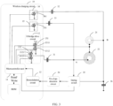
- the electronic device may include a wireless charging circuit 10, an antenna module 20, and a matching circuit 30.
- the matching circuit 30 may include a first resonant capacitor 31, a first load modulation capacitor 32, a second load modulation capacitor 33, and an envelope detection circuit 34.
- a first resonant capacitor 31 a first load modulation capacitor 32
- a second load modulation capacitor 33 a second load modulation capacitor 33
- an envelope detection circuit 34 there may be one or more first resonant capacitors 31, first load modulation capacitors 32, and second load modulation capacitors 33. This may be specifically determined according to an actual requirement, and is not limited in this embodiment of this application.
- the wireless charging circuit 10 may include a microcontroller unit 11, a demodulation circuit 12, an H-bridge drive circuit 13, a first load modulation circuit 14, and a second load modulation circuit 15.
- the H-bridge drive circuit 13 may include a first half-bridge drive circuit 131 and a second half-bridge drive circuit 132, a first end of the first half-bridge drive circuit 131 and a first end of the second half-bridge drive circuit 132 are each electrically connected to a power supply end (VCC), a second end of the first half-bridge drive circuit and a second end of the second half-bridge drive circuit are each grounded, and the first half-bridge drive circuit 131 is electrically connected to the second half-bridge drive circuit 132 sequentially by using the antenna module 20 and the first resonant capacitor 31.
- VCC power supply end
- the first load modulation circuit 14 is separately electrically connected to the antenna module 20 and the envelope detection circuit 34 by using the first load modulation capacitor 32
- the second load modulation circuit 15 is separately electrically connected to the antenna module 20, the first resonant capacitor 31, and the envelope detection circuit 34 by using the second load modulation capacitor 33
- the envelope detection circuit 34 is further electrically connected to the demodulation circuit 12.
- the microcontroller unit 11 is separately electrically connected to the demodulation circuit 12, the first load modulation circuit 14, the second load modulation circuit 15, the first half-bridge drive circuit 131, and the second half-bridge drive circuit 132.
- the wireless charging circuit 10 may be an Integrated Circuit (Integrated Circuit, IC).
- the wireless charging circuit 10 may be referred to as a wireless charging IC.
- the wireless charging circuit 10 may not be integrated. This may be specifically determined according to an actual situation, and is not limited in this embodiment of this application.
- the H-bridge drive circuit 13 may be configured to drive the antenna module 20 to operate in a wireless charging transmit mode, a wireless charging receive mode, an RFID card reader mode, or an RFID card simulation mode.
- the antenna module 20 may include at least one coil.
- the H-bridge drive circuit 13 may be configured to drive some or all of the at least one coil in the antenna module to oscillate, so as to implement wireless charging, reverse wireless charging, RFID card identification, or RFID card simulation. Therefore, the H-bridge drive circuit may also be referred to as a coil drive circuit or an H-bridge coil drive circuit.
- the H-bridge drive circuit 13 may drive a coil to oscillate by using one half-bridge drive circuit.
- the H-bridge drive circuit 13 is in a half-bridge drive mode.
- the H-bridge drive circuit 13 may drive a coil by using two half-bridge drive circuits. In this case, it may be considered that the H-bridge drive circuit 13 is in an H-bridge drive mode.
- the first load modulation circuit 14 and the second load modulation circuit 15 may be configured to perform load modulation, so as to perform protocol communication with a wireless charging transmit device or implement card number sending.
- the envelope detection circuit 34 may be configured to filter a carrier and reserve a baseband signal.
- the demodulation circuit 12 may be configured to demodulate a baseband signal to obtain a charging power expected by a charging receive device or a card number of an RFID card.
- the envelope detection circuit 34 and the demodulation circuit 12 may be configured to: determine a transmit power of the antenna module 20, where the transmit power is determined based on a charging power expected by the charging receive device; and determine the card number of the RFID card.
- the RFID card may be an entity RFID card, or may be an analog RFID card.
- the electronic device may further include another component, such as an application processor that is configured to implement overall control of the electronic device, and may store a card number and send the card number in a wireless communication manner or a Universal Serial Bus (Universal Serial Bus, USB) connection manner.
- an application processor that is configured to implement overall control of the electronic device, and may store a card number and send the card number in a wireless communication manner or a Universal Serial Bus (Universal Serial Bus, USB) connection manner.
- USB Universal Serial Bus
- an operating mode of the electronic device may include a wireless charging receive mode, a wireless charging transmit mode, an RFID card reader mode, and an RFID card simulation mode.
- the electronic device is equivalent to the wireless charging receive device, and may perform the following operations: implementing load modulation by using a load modulation circuit, so as to perform protocol communication with the wireless charging transmit device, and driving a coil in the antenna module to oscillate to implement full-bridge rectification effect, thereby implementing wireless charging.
- the electronic device is equivalent to the wireless charging transmit device, and may perform the following operations: driving a coil in the antenna module to implement reverse wireless charging, and determining the transmit power of the antenna module by using the envelope detection circuit and the demodulation circuit.
- the electronic device is equivalent to an RFID card reader device, and may perform the following operations: driving a coil in the antenna module to implement a card reader function, and determining the card number of the RFID card by using the envelope detection circuit and the demodulation circuit.
- the electronic device is in the RFID card simulation mode, the electronic device is equivalent to an RFID card, and may implement load modulation by using a load modulation circuit, so as to implement card number sending.
- the wireless charging transmit mode (or the RFID card reader mode) may be specifically implemented in the following manner: As shown in FIG. 2 , the H-bridge drive circuit 13 may drive a coil in the antenna module 20 to oscillate, radiate outward, and transmit a carrier signal. After receiving the carrier signal, the wireless charging receive device (or the RFID card) starts load modulation, so that an amplitude of a carrier changes, and a carrier signal with a load modulation signal is formed on one end of the coil near a resonant capacitor. The carrier with the load modulation signal is transmitted to the envelope detection circuit 34, and the envelope detection circuit 34 filters out the carrier, reserves a baseband signal, and transmits the baseband signal to the demodulation circuit 12. The demodulation circuit 12 is configured to demodulate the baseband signal to obtain the charging power expected by the charging receive device (or the card number of the RFID card).
- the wireless charging receive mode, the wireless charging transmit mode, the RFID card reader mode, and the RFID card simulation mode may be implemented by sharing at least one of the following: a wireless charging circuit, a coil, and a matching circuit. Specific descriptions are as follows.
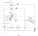
- the antenna module 20 may include a radio frequency identification RFID coil 21 and a wireless charging coil 22, the matching circuit may further include a gating switch 35 and a second resonant capacitor 36.
- a first end of the second resonant capacitor 36 is electrically connected to the first load modulation circuit 14 by using the first load modulation capacitor 32, and a second end of the second resonant capacitor 36 is grounded.
- the gating switch 35 is separately electrically connected to a first point (denoted as A in the figure), a second point (denoted as B in the figure), the envelope detection circuit 34, and the microcontroller unit 11.
- the first point is a common point between the first resonant capacitor 31 and a second end of the wireless charging coil 22, and the second point is a common point between the first load modulation capacitor 32 and the second resonant capacitor 36.
- a first end of the RFID coil 21 is electrically connected to the first half-bridge drive circuit 131, and a second end of the RFID coil 21 is electrically connected to the second point.
- a first end of the wireless charging coil 22 is electrically connected to the first half-bridge drive circuit 131, and the second end of the wireless charging coil 22 is electrically connected to the second half-bridge drive circuit 132 by using the first resonant capacitor 31.
- the second load modulation circuit 15 is electrically connected to the first point by using the second load modulation capacitor 33.
- the first load modulation circuit 14 may be configured to send a card number.
- the second load modulation circuit 15 is configured to implement protocol communication with the wireless charging transmit device.
- the RFID coil 21 is configured to implement card number identification of the RFID card.
- the wireless charging coil 22 is configured to implement wireless charging or reverse wireless charging. Therefore, the second resonant capacitor 36 connected to the RFID coil 21 may be referred to as an RFID resonant capacitor, and the first load modulation capacitor 32 connected to the RFID coil 21 may be referred to as an RFID load modulation capacitor.
- the first resonant capacitor 31 connected to the wireless charging coil 22 may be referred to as a wireless charging resonant capacitor, and the second load modulation capacitor 33 connected to the wireless charging coil 22 may be referred to as a wireless charging load modulation capacitor.
- the gating switch 35 may connect the envelope detection circuit 34 and the first point. In this case, the envelope detection circuit 34 and the demodulation circuit 12 are configured to determine the charging power expected by the wireless charging receive device.
- the gating switch 35 may alternatively connect the envelope detection circuit 34 and the second point. In this case, the envelope detection circuit 34 and the demodulation circuit 12 are configured to determine the card number of the RFID card.
- the wireless charging coil 22 and the RFID coil 21 are completely independently designed, the wireless charging circuit is shared, the resonant capacitor and the load modulation capacitor in the matching circuit are independently designed, and the envelope detection circuit 34 is shared by using the gating switch 35, so that the electronic device supports a wireless charging receive function, a wireless charging transmit function, an RFID card reader function, and an RFID card simulation function.
- the following describes operating states of the electronic device in different operating modes.
- the electronic device may perform protocol communication with the wireless charging transmit device by using the second load modulation circuit 15, and may drive the wireless charging coil 22 by using the H-bridge drive circuit 13 to implement wireless charging.
- the electronic device may control the first load modulation circuit 14 to be in an off state, so as to reduce power consumption.
- the electronic device may control the second load modulation circuit 15 to be in an on state or an off state alternately according to a first preset frequency, so as to perform protocol communication with the wireless charging transmit device.
- the H-bridge drive circuit 13 may drive the wireless charging coil 22 to oscillate by using the H-bridge drive mode, to implement full-bridge rectification effect, thereby implementing wireless charging.
- the microcontroller unit 11 may control the first half-bridge drive circuit 131 and the second half-bridge drive circuit 132 to alternately connect to the power supply end or be grounded at a second preset frequency, that is, at a same moment, one of the first half-bridge drive circuit 131 and the second half-bridge drive circuit 132 is connected to the power supply end but is not grounded, and the other half-bridge drive circuit is not connected to the power supply end but is grounded.
- the first half-bridge drive circuit 131 may be controlled to connect to the power supply end, and the second half-bridge drive circuit 132 is controlled to be grounded. Then, the first half-bridge drive circuit 131 is controlled to be grounded, and the second half-bridge drive circuit 132 is controlled to connect to the power supply end.
- the power supply end of the first half-bridge drive circuit 131, the wireless charging coil 22, the wireless charging resonant capacitor, and the ground of the second half-bridge drive circuit 132 form a path, and a current flows from the power supply end connected to the first half-bridge drive circuit 131 to the ground of the second half-bridge drive circuit 132 to form a forward current.
- the ground of the first half-bridge drive circuit 131, the wireless charging coil 22, the wireless charging resonant capacitor, and the power supply end of the second half-bridge drive circuit 132 form a path, and a current flows from the power supply end connected to the second half-bridge drive circuit 132 to the ground of the first half-bridge drive circuit 131 to form a reverse current.
- first half-bridge drive circuit 131 and the second half-bridge drive circuit 132 are alternately connected to the power supply end and grounded, a reciprocal oscillating current is formed, so that an oscillating voltage of the coil of the wireless charging transmit device changes, to implement full-bridge rectification effect, thereby implementing wireless charging.
- the electronic device may drive the wireless charging coil 22 by using the H-bridge drive circuit 13 to implement wireless charging.
- the H-bridge drive circuit 13 may drive the wireless charging coil 22 to oscillate by using the H-bridge drive mode, thereby implementing reverse wireless charging.
- the microcontroller unit 11 may control the first half-bridge drive circuit 131 and the second half-bridge drive circuit 132 to alternately connect to the power supply end or be grounded at a second preset frequency.
- the gating switch 35 may connect the envelope detection circuit 34 and the first point, so that after demodulating a load modulation signal, the envelope detection circuit 34 and the demodulation circuit 12 may obtain the charging power expected by the charging receive device, and the electronic device may be further triggered to adjust the transmit power of the antenna module 20.
- the electronic device may control the first load modulation circuit 14 and the second load modulation circuit 15 to be in an off state, so as to reduce power consumption.
- the electronic device may drive the RFID coil 21 by using the H-bridge drive circuit 13 to implement card number identification of the RFID card.
- the electronic device may control the second half-bridge drive circuit 132 to be in an off state. In this case, the H-bridge drive circuit 13 is in the half-bridge drive mode.
- the microcontroller unit 11 may control the first half-bridge drive circuit 131 to alternately connect to the power supply end or be grounded, that is, at a same moment, the first half-bridge drive circuit 131 is connected to the power supply end or grounded.
- the first half-bridge drive circuit 131 may be controlled to connect to the power supply end but not to be grounded. Then, the first half-bridge drive circuit 131 is controlled to be grounded but not to connect to the power supply end.
- the power supply end of the first half-bridge drive circuit 131, a third coil 25, the second resonant capacitor 36, and the ground form a path, and a current flows from the power supply end connected to the first half-bridge drive circuit 131 to the ground to form a forward current.
- the second resonant capacitor 36, a third coil 25, and the ground of the first half-bridge drive circuit 131 form a path, and a current flows from the second resonant capacitor 36 to the ground of the first half-bridge drive circuit 131 to form a reverse current.
- the gating switch 35 may connect the envelope detection circuit 34 and the second point.
- the envelope detection circuit 34 and the demodulation circuit 12 may learn the card number of the RFID card after demodulating a load modulation signal.
- the electronic device may control the first load modulation circuit 14 and the second load modulation circuit 15 to be in an off state, so as to reduce power consumption.
- the electronic device may implement card number sending by using the first load modulation circuit 14 and the first half-bridge drive circuit 131.
- a loop current may be formed or a current loop may be disconnected on a path in which the first load modulation circuit 14 and the first half-bridge drive circuit 131 are located. In the circuit path, as long as one end of the circuit path is disconnected, the path may be disconnected. Therefore, card number sending may be performed by using the first load modulation circuit 14 and the first half-bridge drive circuit 131 in the following manner:
- the electronic device may control the second load modulation circuit 15, the first load modulation circuit 14, and the second load modulation circuit 15 to be in an off state, so as to reduce power consumption.
- the antenna module 20 includes a first coil 23.
- the first coil 23 includes a drive common (COM) terminal, a wireless power charge (Wireless Power Charge, WPC) terminal, and an RFID terminal, and the WPC terminal is located between the drive common terminal and the RFID terminal.
- the matching circuit further includes a gating switch 35, a second resonant capacitor 36, and a first switch 37.
- the gating switch 35 is separately electrically connected to a first point, a second point, the envelope detection circuit 34, and the microcontroller unit 11, the first point is a common point between the first resonant capacitor 31 and the WPC terminal, and the second point is a common point between the second resonant capacitor 36 and the first load modulation capacitor 32.
- the drive common terminal is electrically connected to the first half-bridge drive circuit 131, the WPC terminal is electrically connected to the second half-bridge drive circuit 132 by using the first resonant capacitor 31, and the RFID terminal is electrically connected to the second point.
- the second load modulation circuit 15 is electrically connected to the first point by using the second load modulation capacitor 33.
- the first load modulation circuit 14 may be configured to send a card number.
- the second load modulation circuit 15 is configured to implement protocol communication with the wireless charging transmit device.
- a part between the drive COM terminal and the WPC terminal of the first coil 23 may be equivalent to a wireless charging coil, and may be configured to implement wireless charging or reverse wireless charging.
- a part between the drive COM terminal of the first coil 23 and the RFID terminal may be equivalent to an RFID identification coil, and may be configured to implement card number identification of the RFID card. Therefore, the second resonant capacitor 36 connected to the RFID terminal of the first coil 23 may be referred to as an RFID resonant capacitor, and the first load modulation capacitor 32 connected to the RFID terminal of the first coil 23 may be referred to as an RFID load modulation capacitor.
- the first resonant capacitor 31 connected to the WPC terminal of the first coil 23 may be referred to as a wireless charging resonant capacitor, and the second load modulation capacitor 33 connected to the WPC terminal of the first coil 23 may be referred to as a wireless charging load modulation capacitor.
- the electronic device shares some coils so that the electronic device implements the RFID identification technology and the wireless charging technology.
- the RFID identification technology and the wireless charging technology share some coils.
- the second resonant capacitor 36 and the first switch 37 are added.
- a gating switch 35 is added, so that the envelope detection circuit 34 and the demodulation circuit 12 separately perform signal demodulation in different technologies.
- the gating switch 35 may connect the envelope detection circuit 34 and the first point.
- the envelope detection circuit 34 and the demodulation circuit 12 are configured to determine the charging power expected by the wireless charging receive device.
- the gating switch 35 may alternatively connect the envelope detection circuit 34 and the second point.
- the envelope detection circuit 34 and the demodulation circuit 12 are configured to determine the card number of the RFID card.
- the following describes operating states of the electronic device in different operating modes.
- the electronic device may perform protocol communication with the wireless charging transmit device by using the second load modulation circuit 15, and may drive a part of the drive COM terminal and the WPC terminal of the first coil 23 by using the H-bridge drive circuit 13 to implement wireless charging.
- the electronic device may control the first load modulation circuit 14 to be in an off state, so as to reduce power consumption.
- the electronic device may control the second load modulation circuit 15 to be in an on state or an off state alternately according to a first preset frequency, so as to perform protocol communication with the wireless charging transmit device.
- the H-bridge drive circuit 13 may drive the part of the drive COM terminal and the WPC terminal of the first coil 23 to oscillate by using the H-bridge drive mode, to implement full-bridge rectification effect, thereby implementing wireless charging.
- the microcontroller unit 11 may control the first half-bridge drive circuit 131 and the second half-bridge drive circuit 132 to alternately connect to the power supply end or be grounded at a second preset frequency, so that an oscillating voltage of the coil of the wireless charging transmit device changes, to implement full-bridge rectification effect, thereby implementing wireless charging.
- the related description of Implementation 1 Details are not described herein.
- the RFID identification technology and the wireless charging technology share some coils.
- the microcontroller unit 11 may control the first switch 37 to keep an off state.
- the electronic device may drive a part of the drive COM terminal and the WPC terminal of the first coil 23 by using the H-bridge drive circuit 13 to implement wireless charging.
- the H-bridge drive circuit 13 may drive the wireless charging coil 22 to oscillate by using the H-bridge drive mode, thereby implementing reverse wireless charging.
- the microcontroller unit 11 may control the first half-bridge drive circuit 131 and the second half-bridge drive circuit 132 to alternately connect to the power supply end or be grounded at a second preset frequency.
- the microcontroller unit 11 may control the first switch 37 to be turned off.
- the gating switch 35 may connect the envelope detection circuit 34 and the first point, so that after demodulating a load modulation signal, the envelope detection circuit 34 and the demodulation circuit 12 may obtain the charging power expected by the charging receive device, and the electronic device may be further triggered to adjust the transmit power of the antenna module 20.
- the electronic device may control the first load modulation circuit 14 and the second load modulation circuit 15 to be in an off state, so as to reduce power consumption.
- the electronic device may drive a part of the drive COM terminal and the RFID terminal of the first coil 23 by using the H-bridge drive circuit 13 to implement card number identification of the RFID card.
- the electronic device may control the second half-bridge drive circuit 132 to be in an off state. In this case, the H-bridge drive circuit 13 is in the half-bridge drive mode.
- the microcontroller unit 11 may control the first half-bridge drive circuit 131 to alternately connect to the power supply end or be grounded, that is, at a same moment, the first half-bridge drive circuit 131 is connected to the power supply end or grounded.
- the gating switch 35 may connect the envelope detection circuit 34 and the second point.
- the envelope detection circuit 34 and the demodulation circuit 12 may learn the card number of the RFID card after demodulating a load modulation signal.
- the electronic device may control the first load modulation circuit 14 and the second load modulation circuit 15 to be in an off state, so as to reduce power consumption.
- Manner 1 The electronic device may implement card number sending by using the first load modulation circuit 14 and the first half-bridge drive circuit 131.
- a loop current may be formed or a current loop may be disconnected on a path in which the first load modulation circuit 14 and the first half-bridge drive circuit 131 are located.
- the first load modulation circuit 14 may be controlled to be in an on state, and the first half-bridge drive circuit 131 is controlled to be grounded. Then, the first load modulation circuit 14 is controlled to be in an off state, and/or the first half-bridge drive circuit 131 is controlled not to be grounded. This is repeated.
- the electronic device may control the second load modulation circuit 15 and the second half-bridge drive circuit 132 to be in an off state, so as to reduce power consumption and avoid interference from a wireless charging function to RFID card simulation.
- the electronic device may implement card number sending by using the first load modulation circuit 14 and the first switch 37.
- a loop current may be formed or a current loop may be disconnected on a path in which the first load modulation circuit 14 and the first switch 37 are located.
- the first load modulation circuit 14 may be controlled to be in an on state, and the first switch 37 is controlled to be turned on. Then, the first load modulation circuit 14 is controlled to be in an off state, and/or the first switch 37 is controlled to be turned off. This is repeated.
- the electronic device may control the second load modulation circuit 15, the first half-bridge drive circuit, and the second half-bridge drive circuit 132 to be in an off state, so as to reduce power consumption and avoid interference from a wireless charging function to RFID card simulation.
- the electronic device may implement card number sending by using the first load modulation circuit 14, the first half-bridge drive circuit 131, and the first switch 37.
- the first load modulation circuit 14 may be controlled to be in an on state, the first half-bridge drive circuit 131 is controlled to be grounded, and the first switch 37 is controlled to be turned on. Then, the first load modulation circuit 14 is controlled to be in an off state, and/or the first half-bridge drive circuit 131 is controlled not to be grounded, and/or the first switch 37 is controlled to be turned off. This is repeated.
- the electronic device may control the second load modulation circuit 15 and the second load modulation circuit 15 to be in an off state, so as to reduce power consumption and avoid interference from a wireless charging function to RFID card simulation.
- the antenna module 20 may include a second coil 24 and a third coil 25.
- the matching circuit further includes a gating switch 35, a second resonant capacitor 36, and a first switch 37.
- a first end of the second resonant capacitor 36 is electrically connected to the first load modulation circuit 14 by using the first load modulation capacitor 32, and a second end of the second resonant capacitor 36 is grounded by using the first switch 37.
- the gating switch 35 is separately electrically connected to a first point, a second point, the envelope detection circuit 34, and the microcontroller unit 11, the first point is a common point between the first resonant capacitor 31 and a second end of the second coil 24, and the second point is a common point between the second resonant capacitor 36 and the first load modulation capacitor 32.
- a first end of the second coil 24 is electrically connected to the first half-bridge drive circuit 131, and the second end of the second coil 24 is electrically connected to the second half-bridge drive circuit 132 by using the first resonant capacitor 31.
- a first end of the third coil 25 is electrically connected to the first half-bridge drive circuit 131, and a second end of the third coil 25 is electrically connected to the second point.
- the second load modulation circuit 15 is electrically connected to the first point by using the second load modulation capacitor 33.
- Implementation 3 A main difference between Implementation 3 and Implementation 1 is that the first switch 37 is added in Implementation 3 relative to Implementation 1, so that the second coil 24 and the third coil 25 can be independently controlled in Implementation 3. Therefore, in Implementation 3, the four operating modes of the electronic device may be implemented by using a single coil, or the four operating modes of the electronic device may be implemented by using a dual coil. This may be specifically determined according to an actual situation, and is not limited in this embodiment of this application.
- the second coil 24 may be configured to implement wireless charging or reverse wireless charging, and/or implementing card number identification of the RFID card.
- the third coil 25 may be configured to implement wireless charging or reverse wireless charging, and/or implementing card number identification of the RFID card.
- the first load modulation circuit 14 may be configured to implement card number sending, and/or implement protocol communication with the wireless charging transmit device.
- the second load modulation circuit 15 may be configured to implement card number sending, and/or implement protocol communication with the wireless charging transmit device.
- the following describes operating states of the electronic device in different operating modes.
- the electronic device may implement wireless charging by using the second coil 24 and/or the third coil 25. This is separately described as follows:
- the microcontroller unit 11 may control the first load modulation circuit 14 to be in an off state, and the first switch 37 is in an off state.
- the microcontroller unit 11 may first control the second load modulation circuit 15 to be in an on state, control the second half-bridge drive circuit 132 to be grounded, then control the second load modulation circuit 15 to be in an off state, and control the second half-bridge drive circuit 132 not to be grounded. This is performed alternately so as to form load modulation, to implement protocol communication with the wireless charging transmit device, and notify the wireless charging transmit device of the charging power required.
- the H-bridge drive circuit 13 may drive the second coil 24 to oscillate by using the H-bridge drive mode, to implement full-bridge rectification effect, thereby implementing wireless charging.
- the microcontroller unit 11 may control the first half-bridge drive circuit 131 and the second half-bridge drive circuit 132 to alternately connect to the power supply end or be grounded at a second preset frequency, so that an oscillating voltage of the coil of the wireless charging transmit device changes, to implement full-bridge rectification effect, thereby implementing wireless charging.
- b) Wireless charging is implemented by using the third coil 25.
- the microcontroller unit 11 may control the second half-bridge drive circuit 132 to be in an off state.
- the microcontroller unit 11 may control the first load modulation circuit 14 and the first switch 37, or control the first load modulation circuit 14 and the first half-bridge drive circuit 131 to form load modulation, to implement protocol communication with the wireless charging transmit device, and notify the wireless charging transmit device of the charging power required.
- the microcontroller unit 11 may first control the first load modulation circuit 14 to be in an on state, control the first switch 37 to be turned on, then control the first load modulation circuit 14 to be in an off state, and control the first switch 37 to be turned off. This is performed alternately.
- the microcontroller unit 11 may first control the first load modulation circuit 14 to be in an on state, control the first half-bridge drive circuit 131 to be grounded, then control the first load modulation circuit 14 to be in an off state, and control the first half-bridge drive circuit 131 not to be grounded. This is performed alternately.
- the H-bridge drive circuit 13 may drive the third coil 25 to oscillate by using the first half-bridge drive circuit 131, to implement full-bridge rectification effect, thereby implementing wireless charging.
- the H-bridge drive circuit 13 is in a half-bridge drive mode.
- the microcontroller unit 11 may control the first half-bridge drive circuit 131 to be alternately connected to the power supply end or be grounded.
- the first switch 37 is controlled to be turned on.
- Wireless charging is implemented by using the second coil 24 and the third coil 25.
- the microcontroller unit 11 may control the first switch 37 to keep an on state.
- the microcontroller unit 11 may control one of the first load modulation circuit 14 and the second load modulation circuit 15 to be regularly on or off, to form load modulation, to implement protocol communication with the wireless charging transmit device, and notify the wireless charging transmit device of the charging power required.
- the H-bridge drive circuit 13 may drive the second coil 24 and the third coil 25 to oscillate by using the H-bridge drive mode.
- the microcontroller unit 11 may control the first half-bridge drive circuit 131 and the second half-bridge drive circuit 132 to alternately connect to the power supply end or be grounded at a second preset frequency, so that an oscillating voltage of the coil of the wireless charging transmit device changes, to implement full-bridge rectification effect, thereby implementing wireless charging.
- the related description of Implementation 1 Details are not described herein.
- the envelope detection circuit 34 and the demodulation circuit 12 may be configured to obtain the charging power expected by the charging receive device, and the electronic device may be further triggered to adjust the transmit power of the antenna module 20.
- the electronic device may perform reverse wireless charging by using the second coil 24 and/or the third coil 25. This is separately described as follows:
- the electronic device may drive the second coil 24 by using the H-bridge drive circuit 13 to implement wireless charging.
- the first switch 37 may be controlled to be turned off.
- the H-bridge drive circuit 13 may drive the wireless charging coil 22 to oscillate by using the H-bridge drive mode, thereby implementing reverse wireless charging.
- the microcontroller unit 11 may control the first half-bridge drive circuit 131 and the second half-bridge drive circuit 132 to alternately connect to the power supply end or be grounded at a second preset frequency.
- the gating switch 35 may connect the envelope detection circuit 34 and the first point.
- the electronic device may control the first load modulation circuit 14 and the second load modulation circuit 15 to be in an off state, so as to reduce power consumption.
- Reverse wireless charging is performed by using the third coil 25.
- the electronic device may drive the third coil 25 by using the H-bridge drive circuit 13 to implement wireless charging.
- the second half-bridge drive circuit 132 may be controlled to be in an off state.
- the H-bridge drive circuit 13 may drive the third coil 25 to oscillate by using the first half-bridge drive circuit 131.
- the H-bridge drive circuit 13 is in a half-bridge drive mode.
- the microcontroller unit 11 may control the first half-bridge drive circuit 131 to be alternately connected to the power supply end or be grounded.
- the first switch 37 is controlled to be turned on. Further, the first switch 37 may be controlled to be always in an on state.
- the gating switch 35 may connect the envelope detection circuit 34 and the second point.
- the electronic device may control the first load modulation circuit 14 and the second load modulation circuit 15 to be in an off state, so as to reduce power consumption.
- Reverse wireless charging is performed by using the second coil 24 and the third coil 25.
- the microcontroller unit 11 may control the first switch 37 to keep an on state.
- the electronic device may drive the third coil 25 and the third coil 25 by using the H-bridge drive circuit 13 to implement wireless charging.
- the H-bridge drive circuit 13 may drive the second coil 24 and the third coil 25 to oscillate by using the H-bridge drive mode.
- the microcontroller unit 11 may control the first half-bridge drive circuit 131 and the second half-bridge drive circuit 132 to alternately connect to the power supply end or be grounded at a second preset frequency.
- the gating switch 35 may alternately connect the envelope detection circuit 34 and the first point or connect the envelope detection circuit 34 and the second point.
- the electronic device may control the first load modulation circuit 14 and the second load modulation circuit 15 to be in an off state, so as to reduce power consumption.
- the envelope detection circuit 34 and the demodulation circuit 12 may learn the card number of the RFID card after demodulating a load modulation signal.
- the electronic device may implement card number identification by using the second coil 24 and/or the third coil 25. This is separately described as follows:
- the first switch 37 may be controlled to be turned off, and the second half-bridge drive circuit 132 is controlled to be grounded.
- the H-bridge drive circuit 13 may be alternately connected to a power supply or be grounded by using the first half-bridge drive circuit 131, so as to drive the second coil 24 to oscillate.
- the gating switch 35 may connect the envelope detection circuit 34 and the first point.
- the electronic device may control the first load modulation circuit 14 and the second load modulation circuit 15 to be in an off state, so as to reduce power consumption.
- Card number identification is implemented by using the third coil 25.
- the first switch 37 may be controlled to be turned on, and the second half-bridge drive circuit 132 is controlled to be in an off state.
- the H-bridge drive circuit 13 may be alternately connected to a power supply or be grounded by using the first half-bridge drive circuit 131, so as to drive the third coil 25 to oscillate.
- the gating switch 35 may connect the envelope detection circuit 34 and the second point.
- the electronic device may control the first load modulation circuit 14 and the second load modulation circuit 15 to be in an off state, so as to reduce power consumption.
- Card number identification is implemented by using the second coil 24 and the third coil 25.
- the second half-bridge drive circuit 132 may be controlled to be grounded, and the first switch 37 is controlled to be turned on.
- the H-bridge drive circuit 13 may be alternately connected to a power supply or be grounded by using the first half-bridge drive circuit 131, so as to drive the second coil 24 and the third coil 25 to oscillate.
- the gating switch 35 may alternately connect the envelope detection circuit 34 and the first point or connect the envelope detection circuit 34 and the second point, to implement data receiving in a time-sharing manner.
- the electronic device may control the first load modulation circuit 14 and the second load modulation circuit 15 to be in an off state, so as to reduce power consumption.
- the electronic device may implement RFID card simulation by using the second coil 24 and/or the third coil 25. This is separately described as follows:
- Manner 1 The electronic device may implement card number sending by using the second load modulation circuit 15 and the first half-bridge drive circuit 131.
- a loop current may be formed or a current loop may be disconnected on a path in which the second load modulation circuit 15 and the first half-bridge drive circuit 131 are located.
- the second load modulation circuit 15 may be controlled to be in an on state, and the first half-bridge drive circuit 131 is controlled to be grounded. Then, the second load modulation circuit 15 is controlled to be in an off state, and/or the first half-bridge drive circuit 131 is controlled not to be grounded. This is repeated.
- the electronic device may control the first load modulation circuit 14 and the second half-bridge drive circuit 132 to be in an off state, so as to reduce power consumption and avoid interference from a wireless charging function to RFID card simulation.
- the electronic device may implement card number sending by using the first half-bridge drive circuit 131 and the second half-bridge drive circuit 132.
- a loop current may be formed or a current loop may be disconnected on a path in which the first half-bridge drive circuit 131 and the second half-bridge drive circuit 132 are located.
- the first half-bridge drive circuit 131 may be first controlled to be grounded, and the second half-bridge drive circuit 132 is controlled to be grounded. Then, the first half-bridge drive circuit 131 is controlled not to be grounded, and/or the second half-bridge drive circuit 132 is controlled to be grounded. This is repeated.
- the electronic device may control the first load modulation circuit 14 and the second load modulation circuit 15 to be in an off state, so as to reduce power consumption.
- the electronic device may implement card number sending by using the second load modulation circuit 15, the first half-bridge drive circuit 131, and the second half-bridge drive circuit 132.
- the second load modulation circuit 15 may be controlled to be in an on state, the first half-bridge drive circuit 131 is controlled to be grounded, and the second half-bridge drive circuit 132 is controlled to be grounded. Then, the second load modulation circuit 15 is controlled to be in an off state, and/or the first half-bridge drive circuit 131 is controlled not to be grounded, and/or the second half-bridge drive circuit 132 is controlled not to be grounded. This is repeated.
- the electronic device may control the first load modulation circuit 14 to be in an off state, so as to reduce power consumption.
- the first switch may be controlled to be turned off, so as to reduce power consumption.
- RFID card simulation is implemented by using the third coil 25.
- Manner 1 The electronic device may implement card number sending by using the first load modulation circuit 14 and the first half-bridge drive circuit 131.
- a loop current may be formed or a current loop may be disconnected on a path in which the first load modulation circuit 14 and the first half-bridge drive circuit 131 are located.
- the first load modulation circuit 14 may be controlled to be in an on state, and the first half-bridge drive circuit 131 is controlled to be grounded. Then, the first load modulation circuit 14 is controlled to be in an off state, and/or the first half-bridge drive circuit 131 is controlled not to be grounded. This is repeated.
- the electronic device may control the second load modulation circuit 15 and the second half-bridge drive circuit 132 to be in an off state, so as to reduce power consumption.
- the electronic device may implement card number sending by using the first load modulation circuit 14 and the first switch 37.
- a loop current may be formed or a current loop may be disconnected on a path in which the first load modulation circuit 14 and the first switch 37 are located.
- the first load modulation circuit 14 may be controlled to be in an on state, and the first switch 37 is controlled to be turned on. Then, the first load modulation circuit 14 is controlled to be in an off state, and/or the first switch 37 is controlled to be turned off. This is repeated.
- the electronic device may control the second load modulation circuit 15, the first half-bridge drive circuit, and the second half-bridge drive circuit 132 to be in an off state, so as to reduce power consumption.
- the electronic device may implement card number sending by using the first load modulation circuit 14, the first half-bridge drive circuit 131, and the first switch 37.
- the first load modulation circuit 14 may be controlled to be in an on state, the first half-bridge drive circuit 131 is controlled to be grounded, and the first switch 37 is controlled to be turned on. Then, the first load modulation circuit 14 is controlled to be in an off state, and/or the first half-bridge drive circuit 131 is controlled not to be grounded, and/or the first switch 37 is controlled to be turned off. This is repeated.
- the electronic device may control the second load modulation circuit 15 and the second load modulation circuit 15 to be in an off state, so as to reduce power consumption.
- RFID card simulation is implemented by using the second coil 24 and the third coil 25.
- the electronic device may implement card number sending by using the first load modulation circuit 14, the second load modulation circuit 15, and the first half-bridge drive circuit 131.
- the electronic device may first control the first load modulation circuit 14 and the second load modulation circuit 15 to be in an on state, and the first half-bridge drive circuit 131 is controlled to be grounded, so as to form a current loop between the second coil 24 and the third coil 25. Then, the first load modulation circuit 14 is controlled to be in an off state, and/or the second load modulation circuit 15 is controlled to be in an off state, and/or the first half-bridge drive circuit 131 is controlled not to be grounded. This is repeated, so that a current is drawn for a coil of an access controller to form a load, and card number sending can be performed.
- the electronic device may control the second half-bridge drive circuit 132 to be in an off state, and control the first switch 37 to be turned off, so as to reduce power consumption.
- the antenna module 20 may include a fourth coil 26.
- a first end of the fourth coil 26 is electrically connected to the second half-bridge drive circuit 132 by using the first resonant capacitor 31, and a second end of the fourth coil 26 is electrically connected to the first half-bridge drive circuit 131.
- the envelope detection circuit 34 is electrically connected to a first point, and the first point is a common point between the first resonant capacitor 31 and the first end of the fourth coil.
- the first load modulation circuit 14 is electrically connected to the first point by using the first load modulation capacitor 32.
- the second load modulation circuit 15 is electrically connected to the first point by using the second load modulation capacitor 33.
- the fourth coil 26 may be configured to implement wireless charging, implement reverse wireless charging, and implement card number sending.
- the RFID identification technology and the wireless charging technology are implemented by using a same coil.
- the first load modulation circuit 14 may be configured to send a card number.
- the second load modulation circuit 15 is configured to implement protocol communication with the wireless charging transmit device. Therefore, the first load modulation capacitor 32 connected to the first load modulation circuit 14 may be referred to as an RFID load modulation capacitor, and the second load modulation capacitor 33 connected to the second load modulation circuit 15 may be referred to as a wireless charging load modulation capacitor.
- the following describes operating states of the electronic device in different operating modes.
- the electronic device may perform protocol communication with the wireless charging transmit device by using the second load modulation circuit 15, and may drive the fourth coil 26 by using the H-bridge drive circuit 13 to implement wireless charging.
- the electronic device may control the first load modulation circuit 14 to be in an off state, so as to reduce power consumption.
- the electronic device may control the second load modulation circuit 15 to be in an on state or an off state alternately according to a first preset frequency, so as to perform protocol communication with the wireless charging transmit device.
- the H-bridge drive circuit 13 may drive the fourth coil 26 to oscillate by using the H-bridge drive mode, to implement full-bridge rectification effect, thereby implementing wireless charging.
- the microcontroller unit 11 may control the first half-bridge drive circuit 131 and the second half-bridge drive circuit 132 to alternately connect to the power supply end or be grounded at a second preset frequency, so as to form a reciprocal oscillating current, so that an oscillating voltage of the coil of the wireless charging transmit device changes, to implement full-bridge rectification effect, thereby implementing wireless charging.
- the microcontroller unit 11 may control the first half-bridge drive circuit 131 and the second half-bridge drive circuit 132 to alternately connect to the power supply end or be grounded at a second preset frequency, so as to form a reciprocal oscillating current, so that an oscillating voltage of the coil of the wireless charging transmit device changes, to implement full-bridge rectification effect, thereby implementing wireless charging.
- the electronic device may drive the fourth coil 26 by using the H-bridge drive circuit 13 to implement wireless charging.
- the H-bridge drive circuit 13 may drive the wireless charging coil 22 to oscillate by using the H-bridge drive mode, thereby implementing reverse wireless charging.
- the microcontroller unit 11 may control the first half-bridge drive circuit 131 and the second half-bridge drive circuit 132 to alternately connect to the power supply end or be grounded at a second preset frequency.
- the electronic device may control the first load modulation circuit 14 and the second load modulation circuit 15 to be in an off state, so as to reduce power consumption.
- the electronic device may drive the fourth coil 26 by using the H-bridge drive circuit 13 to implement card number identification of the RFID card.
- the microcontroller unit 11 may control the first half-bridge drive circuit 131 to alternately connect to the power supply end or be grounded, and control the second half-bridge drive circuit 132 to be grounded, to implement driving of the fourth coil 26.
- the electronic device may control the first load modulation circuit 14 and the second load modulation circuit 15 to be in an off state, so as to reduce power consumption.
- Manner 1 The electronic device may implement card number sending by using the first load modulation circuit 14 and the first half-bridge drive circuit 131.
- a loop current may be formed or a current loop may be disconnected on a path in which the first load modulation circuit 14 and the first half-bridge drive circuit 131 are located.
- the first load modulation circuit 14 may be controlled to be in an on state, and the first half-bridge drive circuit 131 is controlled to be grounded. Then, the first load modulation circuit 14 is controlled to be in an off state, and/or the first half-bridge drive circuit 131 is controlled not to be grounded. This is repeated.
- the electronic device may control the second load modulation circuit 15 and the second half-bridge drive circuit 132 to be in an off state, so as to reduce power consumption.
- the electronic device may implement card number sending by using the second load modulation circuit 15 and the first half-bridge drive circuit 131.
- a loop current may be formed or a current loop may be disconnected on a path in which the second load modulation circuit 15 and the first half-bridge drive circuit 131 are located.
- the second load modulation circuit 15 may be controlled to be in an on state, and the first half-bridge drive circuit 131 is controlled to be grounded. Then, the second load modulation circuit 15 is controlled to be in an off state, and/or the first half-bridge drive circuit 131 is controlled not to be grounded. This is repeated.
- the electronic device may control the first load modulation circuit 14 and the second half-bridge drive circuit 132 to be in an off state, so as to reduce power consumption.
- the electronic device may implement card number sending by using the first half-bridge drive circuit 131 and the second half-bridge drive circuit 132.
- a loop current may be formed or a current loop may be disconnected on a path in which the first half-bridge drive circuit 131 and the second half-bridge drive circuit 132 are located.
- the first half-bridge drive circuit 131 may be first controlled to be grounded, and the second half-bridge drive circuit 132 is controlled to be grounded. Then, the first half-bridge drive circuit 131 is controlled not to be grounded, and/or the second half-bridge drive circuit 132 is controlled to be grounded. This is repeated.
- the electronic device may control the first load modulation circuit 14 and the second load modulation circuit 15 to be in an off state, so as to reduce power consumption.
- the electronic device may implement card number sending by using the first load modulation circuit 14, the second load modulation circuit 15, the first half-bridge drive circuit 131, and the second half-bridge drive circuit 132.
- the first load modulation circuit 14 may be controlled to be in an on state
- the second load modulation circuit 15 is controlled to be in an on state
- the first half-bridge drive circuit 131 is controlled to be grounded
- the second half-bridge drive circuit 132 is controlled to be grounded.
- the first load modulation circuit 14 is controlled to be in an off state
- the second load modulation circuit 15 is controlled to be in an off state
- the first half-bridge drive circuit 131 is controlled not to be grounded
- the second half-bridge drive circuit 132 is controlled to be grounded. This is repeated.
- the first load modulation circuit 14 includes a first field effect MOS transistor 141
- the second load modulation circuit 15 includes a second MOS transistor 151.
- the first MOS transistor 141 and the second MOS transistor 151 are N-type MOS transistors.
- Agate of the first MOS transistor 141 is electrically connected to the microcontroller unit, a drain of the first MOS transistor 141 is electrically connected to the first load modulation capacitor 32, and a source of the first MOS transistor 141 is grounded.
- a gate of the second MOS transistor 151 is electrically connected to the microcontroller unit, a drain of the second MOS transistor 151 is electrically connected to the second load modulation capacitor 33, and a source of the second MOS transistor 151 is grounded.
- the first MOS transistor 141 is turned on.
- the first MOS transistor 141 is turned off.
- the second MOS transistor 151 is turned on.
- the second MOS transistor 151 is turned off.
- the first half-bridge drive circuit 131 includes a third MOS transistor 1311 and a fourth MOS transistor 1312
- the second half-bridge drive circuit 132 includes a fifth MOS transistor 1321 and a sixth MOS transistor 1322.
- the third MOS transistor 1311 and the fifth MOS transistor 1321 are P-type MOS transistors, and the fourth MOS transistor 1312 and the sixth MOS transistor 1322 are N-type MOS transistors.
- Gates of the third MOS transistor 1311, the fourth MOS transistor 1312, the fifth MOS transistor 1321, and the sixth MOS transistor 1322 are each electrically connected to the microcontroller unit 11, sources of the third MOS transistor 1311 and the fifth MOS transistor 1321 are each electrically connected to the power supply end, a drain of the third MOS transistor 1311 is electrically connected to a drain of the fourth MOS transistor 1312, a drain of the fifth MOS transistor 1321 is electrically connected to a drain of the sixth MOS transistor 1322, and sources of the fourth MOS transistor 1312 and the sixth MOS transistor 1322 are each grounded.
- a third point and a fourth point are each electrically connected to the antenna module 20, the third point is a common point between the drain of the third MOS transistor 1311 and the drain of the fourth MOS transistor 1312, and the fourth point is a common point between the drain of the fifth MOS transistor 1321 and the drain of the sixth MOS transistor 1322.
- the third MOS transistor 1311 may be turned on, and the fourth MOS transistor 1312 may be turned off.
- the third MOS transistor 1311 may be turned off, and the fourth MOS transistor 1312 may be turned on.
- the third MOS transistor 1311 and the fourth MOS transistor 1312 are turned off.
- the fifth MOS transistor 1321 may be turned on, and the sixth MOS transistor 1322 may be turned off.
- the fifth MOS transistor 1321 may be turned off, and the sixth MOS transistor 1322 may be turned on.
- the fifth MOS transistor 1321 and the sixth MOS transistor 1322 are turned off.
- the half-bridge drive circuit may alternatively be formed by using another switch. This may be specifically determined according to an actual situation, and is not limited in this embodiment of this application.
- the first switch 37 in FIG. 3 is also represented as a MOS transistor.
- the first switch 37 may alternatively be a switch in another form, such as a single-pole double-throw switch.
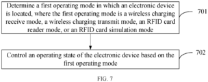
- FIG. 7 is a flowchart of a control method according to an embodiment of this application. As shown in FIG. 7 , the control method may include the following steps:
- an operating mode of the electronic device includes a wireless charging receive mode, a wireless charging transmit mode, an RFID card reader mode, and an RFID card simulation mode, so that the electronic device implements a wireless charging function, an RFID card reader function, and an RFID card simulation function, thereby enriching functions of the electronic device.
- the first load modulation circuit includes the first MOS transistor
- the second load modulation circuit includes the second MOS transistor
- the first half-bridge drive circuit includes the third MOS transistor and the fourth MOS transistor
- the second half-bridge drive circuit includes the fifth MOS transistor and the sixth MOS transistor.
- the first operating mode is a wireless charging receive mode
- the controlling an operating state of the electronic device based on the first operating mode includes:
- the first operating mode is a wireless charging transmit mode
- the controlling an operating state of the electronic device based on the first operating mode includes:
- the first operating mode is an RFID card reader mode
- the controlling an operating state of the electronic device based on the first operating mode includes:
- the first operating mode is an RFID card simulation mode
- the controlling an operating state of the electronic device based on the first operating mode includes:
- the first operating mode is that the first operating mode is a wireless charging receive mode, a wireless charging transmit mode, an RFID card reader mode, or an RFID card simulation mode, for an operating state of each component of the electronic device, refer to the foregoing related description. Details are not described herein.
- the gating switch may be in an off state to reduce power consumption.
- wireless charging IC hardware is shared, wireless charging IC internal software, that is, a control logic of an MCU, is modified, and a 125K low-frequency RFID antenna and a matching path thereof are added, so that a wireless charging function and a 125K low-frequency access control function are simultaneously implemented in a case of a single wireless charging IC.
- the electronic device in this application mainly includes a wireless charging IC, a wireless charging antenna, and a 125K low-frequency RFID antenna.
- the wireless charging IC implements driving of a wireless charging coil, wireless charging energy transmitting and receiving, driving of a 125K low-frequency RFID coil, and signal detecting and receiving, and implements wireless charging and a 125K low-frequency RFID function in a time-sharing manner or simultaneously.
- the wireless charging antenna implements energy and protocol information transmission and receiving during wireless charging.
- the 125K low-frequency RFID antenna implements a low-frequency RFID function.
- the antenna may be shared with the wireless charging antenna in a part of Embodiment 1.
- a design in this application is based on a difference in a shared hardware part in this application, and there are a plurality of embodiments, which may be implemented through turn-on, turn-off, and periodic turn-on and turn-off of the first MOS transistor to the sixth MOS transistor in different operating modes.
- turn-on, turn-off, and periodic turn-on and turn-off of the first MOS transistor to the sixth MOS transistor in different operating modes For a specific embodiment, refer to the following.
- the antenna, the coil, and the antenna coil may be interchanged.
- Embodiment 1 A wireless charging IC is shared, and an antenna is independently designed.
- a wireless charging IC is shared, and a wireless charging antenna is separated from a 125K low-frequency RFID antenna and a matching circuit by independent design.
- a first half-bridge drive circuit (that is, a third MOS transistor and a fourth MOS transistor) of a coil drive circuit is connected to a common drive terminal of the two antennas;
- the apparatus has four operating modes:
- a current may be formed on an RFID coil or a current may not be formed when the path is disconnected, so as to implement a change of a load formed by a primary coil (that is, a coil of a card reader), and implement data sending.
- a primary coil that is, a coil of a card reader
- a current may be drawn to form a load in a manner in which the first MOS transistor and the fourth MOS transistor are turned on.
- Embodiment 2 The wireless charging IC is shared, and the wireless charging coil and the RFID coil are partially shared.
- the apparatus also has four operating modes, and a difference lies in that a special antenna design of the apparatus and a first switch is added to control the RFID antenna to be grounded, to reduce impact.
- the wireless charging antenna and the RFID antenna are partially shared, which is a hybrid antenna technology, as shown in FIG. 4 .
- the coil has three taps that are respectively a common drive terminal of the two antennas, a WPC terminal, and an RFID terminal.
- the common drive terminal of the two antennas is jointly connected to a first half-bridge drive circuit of the wireless charging IC, and the WPC terminal is a central tap of the coil, and is connected to a second half-bridge drive circuit by using a wireless charging resonant capacitor.
- the RFID terminal is an end of a hybrid coil, has a highest inductance value, and is grounded by the first switch and a resonant capacitor.
- This design is similar to Embodiment 1, but a nested design of the coil causes partial sharing of the coil, that is, only a part of the coil is used during wireless charging, and all of the coil is used during RFID communication.
- the apparatus has four operating modes:
- Whether it is turn-on or not in the foregoing three manners can control whether a current is formed on the coil, that is, a load change is formed on a transmitting primary coil, that is, a coil of an access controller or a card reader, to implement data sending.
- a current is formed on the coil
- a load change is formed on a transmitting primary coil, that is, a coil of an access controller or a card reader
- other switches such as the MOS transistor and/or the first switch, need to be in an off state, to avoid impact.
- the apparatus is similar to that in Embodiment 1, and a main change lies in:
- a first antenna and a second antenna are completely independent and need to be arranged separately.
- Embodiment 1 On the basis of Embodiment 1, the functions are implemented without distinction, and functions of two wireless charging antennas and two RFID antennas, or one RFID antenna and one wireless charging antenna can be implemented.
- the first switch for controlling whether a resonant capacitor of the second antenna is grounded is added, which can implement separate control on whether two coils resonate.
- the apparatus has a plurality of operating modes:
- the single-antenna receive mode There are two cases of the single-antenna receive mode, that is, the first antenna and the second antenna.
- the first MOS first switch of the second antenna is first turned off to avoid interference.
- the fourth transistor and the second MOS transistor are turned on or off simultaneously, to form load modulation, and a charging power required by the other party is notified. Then, energy is received.
- the third MOS transistor to the sixth MOS transistor are periodically turned on to perform energy receiving.
- the fifth MOS transistor and the sixth MOS transistor are first turned off, so as to avoid interference of the first antenna.
- the first MOS transistor and the first switch are turned on or off simultaneously, so that load modulation may be formed (similarly, this may alternatively be implemented by turning on or off the first MOS transistor and the fourth MOS transistor simultaneously), and a power required by the other party is notified.
- the third MOS transistor and the fourth MOS transistor are discontinuously turned on or off, so that energy is received.
- the third MOS transistor is turned on, the first switch is turned on.
- the wireless charging antenna induces a voltage to wake up a wireless charging IC.
- the wireless charging IC implements load modulation by using a "wireless charging communication load modulation control circuit" and implements protocol communication with a wireless charging base, to implement charging.
- MOS transistor switching description The first switch is turned on (to implement resonance of the second antenna), one of the first MOS transistor or the second MOS transistor is regularly turned on or off (required for a wireless charging protocol communication function), and the third MOS transistor to the sixth MOS transistor are regularly turned on or off at a carrier frequency, to implement full-bridge rectification effect, thereby implementing wireless charging.
- the coil drive circuit drives the wireless charging antenna to oscillate and emit energy.
- a corresponding receive device draws energy through load modulation, so that an oscillating voltage of a coil at a transmit end changes.
- an envelope detection circuit and an “internal demodulation circuit” implement demodulation of a load modulation signal, and then send a corresponding power according to a requirement of the other party.
- the first antenna or the second antenna may be separately used for reverse wireless charging.
- the first MOS transistor, the second MOS transistor, and the first switch are turned off, the gating switch is switched to the first antenna, and the third MOS transistor to the sixth MOS transistor drive the first antenna to oscillate.
- a duty cycle of the third MOS transistor to the sixth MOS transistor may be adjusted to adjust the power, thereby implementing reverse wireless charging.
- the first MOS transistor, the second MOS transistor, the fifth MOS transistor, and the sixth MOS transistor are turned off, so as to avoid impact of the first antenna.
- the gating switch is switched to the second antenna, and the third MOS transistor and the fourth MOS transistor are discontinuously connected to form a drive.
- a turn-on duty cycle of the third MOS transistor and the fourth MOS transistor may be adjusted to adjust the transmit power, so as to implement wireless charging transmitting.
- the third MOS transistor is turned on, the first switch is turned on.
- the coil drive circuit drives the wireless charging antenna to oscillate and emit energy.
- a corresponding receive device draws energy through load modulation, so that an oscillating voltage of a coil at a transmit end changes.
- an envelope detection circuit and an “internal demodulation circuit” implement demodulation of a load modulation signal, and then send a corresponding power according to a requirement of the other party.
- MOS transistor switching description The first switch is turned on (to implement resonance of the second coil), and a gating switch at a front end of an envelope detection circuit is periodically switched, so as to implement receiving of data in a polling manner.
- the first MOS transistor and the second MOS transistor are turned on (which is not required by the wireless charging transmit end), and the gating switch is periodically switched.
- the third MOS transistor and the sixth MOS transistor are regularly turned on and off at a carrier frequency, so as to drive the two coils simultaneously, thereby implementing reverse wireless charging by the two coils.
- the receive device may be a single wireless charging receive device having two coils or two wireless charging receive devices each having a single coil.
- 125K low-frequency RFID card reader mode Similar to the foregoing reverse wireless charging mode, the coil drive circuit drives the antenna to oscillate, an RFID card tag is energized to start after approaching a coil, and draws energy through load modulation, so that an oscillating voltage of a coil at a transmit end changes.
- an "envelope detection circuit” and an “internal demodulation circuit” implement demodulation of a load modulation signal, and then learn card number information of the RFID card tag approaching.
- the card reader mode may be divided into a single-antenna mode or a dual-antenna mode, which is described in the following:
- a load modulation module inside the wireless charging IC implements load modulation by turning on or turning off a "125K low-frequency RFID load modulation circuit", and finally implements card number sending.
- the card simulation mode may be divided into a single-antenna mode or a dual-antenna mode, which is described in the following:
- the foregoing function modes may be performed simultaneously by using a single or a plurality of combinations.
- different capacitance values may be configured on resonant capacitors of the first antenna and the second antenna to implement different resonance frequencies, so as to support wireless charging technologies and standards of a plurality of frequencies.
- the load modulation capacitor may be a combination of one or more capacitors, or even a resistor, to achieve a better effect.
- Embodiment 4 A wireless charging IC is shared, and an antenna is completely shared.
- a first half-bridge drive circuit (a third MOS transistor and a fourth MOS transistor) is connected to a COM terminal of antennas;
- the apparatus has four operating modes:
- Manner 1 A current is drawn to form a load in a manner in which the first MOS transistor and the fourth MOS transistor are turned on.
- Manner 2 A current is drawn to form a load in a manner in which the second MOS transistor and the fourth MOS transistor are turned on.
- Manner 3 A current is drawn to form a load in a manner in which the fourth MOS transistor and the sixth MOS transistor are turned on.
- Manner 4 A current is drawn to form a load in a manner in which the first MOS transistor, the second MOS transistor, the fourth MOS transistor, and the sixth MOS transistor are turned on.
Landscapes
- Engineering & Computer Science (AREA)
- Computer Networks & Wireless Communication (AREA)
- Physics & Mathematics (AREA)
- Health & Medical Sciences (AREA)
- Toxicology (AREA)
- Theoretical Computer Science (AREA)
- General Physics & Mathematics (AREA)
- Power Engineering (AREA)
- Artificial Intelligence (AREA)
- General Health & Medical Sciences (AREA)
- Computer Vision & Pattern Recognition (AREA)
- Electromagnetism (AREA)
- Signal Processing (AREA)
- General Engineering & Computer Science (AREA)
- Near-Field Transmission Systems (AREA)
Applications Claiming Priority (2)
| Application Number | Priority Date | Filing Date | Title |
|---|---|---|---|
| CN202111095325.9A CN113780501B (zh) | 2021-09-17 | 2021-09-17 | 电子设备及控制方法 |
| PCT/CN2022/118418 WO2023040824A1 (zh) | 2021-09-17 | 2022-09-13 | 电子设备及控制方法 |
Publications (3)
| Publication Number | Publication Date |
|---|---|
| EP4404100A1 true EP4404100A1 (de) | 2024-07-24 |
| EP4404100A4 EP4404100A4 (de) | 2025-03-26 |
| EP4404100B1 EP4404100B1 (de) | 2026-01-21 |
Family
ID=78852049
Family Applications (1)
| Application Number | Title | Priority Date | Filing Date |
|---|---|---|---|
| EP22869193.7A Active EP4404100B1 (de) | 2021-09-17 | 2022-09-13 | Elektronische vorrichtung und steuerungsverfahren |
Country Status (4)
| Country | Link |
|---|---|
| US (1) | US12511505B2 (de) |
| EP (1) | EP4404100B1 (de) |
| CN (1) | CN113780501B (de) |
| WO (1) | WO2023040824A1 (de) |
Families Citing this family (5)
| Publication number | Priority date | Publication date | Assignee | Title |
|---|---|---|---|---|
| CN113780501B (zh) | 2021-09-17 | 2025-02-18 | 维沃移动通信有限公司 | 电子设备及控制方法 |
| CN113708512B (zh) * | 2021-09-17 | 2025-01-24 | 维沃移动通信有限公司 | 电子设备及控制方法 |
| CN114640377B (zh) * | 2022-03-02 | 2023-08-15 | 维沃移动通信有限公司 | 实体卡添加方法、装置、设备和存储介质 |
| CN117294030A (zh) * | 2022-06-20 | 2023-12-26 | 华为技术有限公司 | 一种无线充电芯片、感应装置及电子设备 |
| CN114899922A (zh) * | 2022-06-20 | 2022-08-12 | 维沃移动通信有限公司 | 无线充电设备、电子设备及其充电方法和装置 |
Family Cites Families (25)
| Publication number | Priority date | Publication date | Assignee | Title |
|---|---|---|---|---|
| JP2005151257A (ja) * | 2003-11-17 | 2005-06-09 | Pegasus Net Kk | Rfid通信における2周波通信方式 |
| CN101330334B (zh) * | 2008-03-04 | 2011-08-10 | 国民技术股份有限公司 | 一种用于校准射频sim卡通信距离的装置及方法 |
| US9130407B2 (en) * | 2008-05-13 | 2015-09-08 | Qualcomm Incorporated | Signaling charging in wireless power environment |
| WO2010019961A2 (en) * | 2008-08-15 | 2010-02-18 | Ivi Smart Technologies, Inc. | Rf power conversion circuits & methods, both for use in mobile devices |
| US8390249B2 (en) * | 2009-11-30 | 2013-03-05 | Broadcom Corporation | Battery with integrated wireless power receiver and/or RFID |
| JP2012090175A (ja) * | 2010-10-21 | 2012-05-10 | Sony Corp | 送信装置、および受信装置 |
| CN102932025A (zh) * | 2012-10-25 | 2013-02-13 | 武汉大学 | 一种基于磁共振的无线能量及信号协同传输系统 |
| US9559544B2 (en) * | 2013-03-15 | 2017-01-31 | Jay Marketing Associates, Inc. | Wireless interrogation and wireless charging of electronic devices |
| CN103595145B (zh) * | 2013-10-31 | 2015-08-05 | 浙江大学 | 一种基于公共电感耦合实现高速通讯和无线能量传输的系统 |
| WO2016127815A1 (zh) * | 2015-02-11 | 2016-08-18 | 天地融科技股份有限公司 | 电子设备 |
| CN104866888B (zh) * | 2015-04-20 | 2018-03-06 | 卓捷创芯科技(深圳)有限公司 | 适用于脉宽调制的调幅信号的整流电路和无源射频标签 |
| CN204631912U (zh) * | 2015-05-29 | 2015-09-09 | 成都华气厚普电子技术有限公司 | 一种射频卡读卡装置 |
| JP6519386B2 (ja) | 2015-07-30 | 2019-05-29 | アイシン精機株式会社 | アンテナ駆動装置 |
| JP5995022B1 (ja) * | 2015-09-10 | 2016-09-21 | パナソニックIpマネジメント株式会社 | 無線電力伝送システムおよび送電装置 |
| US10461583B2 (en) * | 2015-11-10 | 2019-10-29 | Samsung Electronics Co., Ltd. | Electronic device and method for wireless charging in electronic device |
| CN106997481B (zh) * | 2016-01-22 | 2020-04-07 | 中芯国际集成电路制造(上海)有限公司 | 一种rfid系统的电子标签的解调电路 |
| CN108781094B (zh) * | 2016-03-08 | 2021-09-28 | 皇家飞利浦有限公司 | 无线感应功率传输 |
| EP3316182A1 (de) * | 2016-10-27 | 2018-05-02 | Melexis Technologies SA | Verfahren und treiberschaltung für resonanzantennenschaltung |
| CN106849387B (zh) * | 2017-02-28 | 2024-07-19 | 深圳市禾家欢科技有限公司 | 一种无线充电发射装置及其智能充电输入和输出方法 |
| CN206564594U (zh) * | 2017-03-24 | 2017-10-17 | 深圳市文鼎创数据科技有限公司 | 一种多天线近场通信调制解调装置及动态令牌 |
| CN207939234U (zh) * | 2018-03-07 | 2018-10-02 | 深圳市华昌德电子有限公司 | 一种低功耗qi无线充电电路 |
| CN111415476A (zh) * | 2020-04-26 | 2020-07-14 | 艾体威尔电子技术(北京)有限公司 | 一种pos机的无线充电实现方法及系统 |
| CN213876801U (zh) * | 2020-12-17 | 2021-08-03 | 深圳数马电子技术有限公司 | 一种射频识别标签 |
| CN113255382B (zh) * | 2021-05-28 | 2021-10-19 | 卓捷创芯科技(深圳)有限公司 | 一种射频场包络峰值检测信号驱动的放电控制电路和方法 |
| CN113780501B (zh) * | 2021-09-17 | 2025-02-18 | 维沃移动通信有限公司 | 电子设备及控制方法 |
-
2021
- 2021-09-17 CN CN202111095325.9A patent/CN113780501B/zh active Active
-
2022
- 2022-09-13 EP EP22869193.7A patent/EP4404100B1/de active Active
- 2022-09-13 WO PCT/CN2022/118418 patent/WO2023040824A1/zh not_active Ceased
-
2024
- 2024-03-17 US US18/607,512 patent/US12511505B2/en active Active
Also Published As
| Publication number | Publication date |
|---|---|
| EP4404100B1 (de) | 2026-01-21 |
| WO2023040824A1 (zh) | 2023-03-23 |
| CN113780501A (zh) | 2021-12-10 |
| CN113780501B (zh) | 2025-02-18 |
| US12511505B2 (en) | 2025-12-30 |
| US20240220748A1 (en) | 2024-07-04 |
| EP4404100A4 (de) | 2025-03-26 |
Similar Documents
| Publication | Publication Date | Title |
|---|---|---|
| EP4404100B1 (de) | Elektronische vorrichtung und steuerungsverfahren | |
| KR101319146B1 (ko) | 수신 안테나 임피던스 변조를 통한 역방향 링크 시그널링 | |
| EP2830228B1 (de) | HF-Vorrichtung und Verfahren mit verbesserter aktiver Belastungsmodulationskapazität | |
| US10432268B2 (en) | Contactless communication and contactless charging in a system | |
| JP2020504442A (ja) | 電力のワイヤレス伝送のためのシステム | |
| CN117875351A (zh) | 增加rfid标签灵敏度的方法 | |
| JP3607585B2 (ja) | 非接触応答装置 | |
| CN105306105B (zh) | 通信电路及具有调制的通信方法 | |
| US11405074B2 (en) | NFC interface with energy management function | |
| EP4687303A1 (de) | Schaltungseinheiten zur implementierung von nahfeldkommunikation und nfc-vorrichtungen | |
| CN105897312A (zh) | 一种为能量采集和小尺寸优化的nfc标签接口 | |
| CN113746507A (zh) | 一种nfc线圈和无线充电线圈的芯片控制电路及方法 | |
| CN113708512B (zh) | 电子设备及控制方法 | |
| US20120163049A1 (en) | Apparatus for collecting wireless energy and wireless electronic label employing the apparatus | |
| CN109698713B (zh) | 具有能量管理功能的nfc接口 | |
| CN103646263A (zh) | Rfid级联通道装置 | |
| CN105897313A (zh) | 一种优化能量采集及实现小尺寸天线的nfc通信系统及方法 | |
| CN203871470U (zh) | 高频多通道复用射频识别天线 | |
| CN112531322B (zh) | 一种多rfid标签识别的高频天线复用方法 | |
| CN202694400U (zh) | 一种具有高激活性能的有源电子标签 | |
| EP4016390A1 (de) | Rfid-etikett für zwei systeme | |
| CN207234767U (zh) | 一种近场通信nfc电路和终端 | |
| CN223539200U (zh) | 读卡电路和近场通信设备 | |
| CN217692821U (zh) | 一种使用线圈进行充电和通信的系统 | |
| CN120601910A (zh) | Nfc控制器 |
Legal Events
| Date | Code | Title | Description |
|---|---|---|---|
| STAA | Information on the status of an ep patent application or granted ep patent |
Free format text: STATUS: THE INTERNATIONAL PUBLICATION HAS BEEN MADE |
|
| PUAI | Public reference made under article 153(3) epc to a published international application that has entered the european phase |
Free format text: ORIGINAL CODE: 0009012 |
|
| STAA | Information on the status of an ep patent application or granted ep patent |
Free format text: STATUS: REQUEST FOR EXAMINATION WAS MADE |
|
| 17P | Request for examination filed |
Effective date: 20240415 |
|
| AK | Designated contracting states |
Kind code of ref document: A1 Designated state(s): AL AT BE BG CH CY CZ DE DK EE ES FI FR GB GR HR HU IE IS IT LI LT LU LV MC MK MT NL NO PL PT RO RS SE SI SK SM TR |
|
| DAV | Request for validation of the european patent (deleted) | ||
| DAX | Request for extension of the european patent (deleted) | ||
| REG | Reference to a national code |
Ref country code: DE Ref legal event code: R079 Free format text: PREVIOUS MAIN CLASS: G06K0017000000 Ipc: H02J0050120000 Ref country code: DE Ref legal event code: R079 Ref document number: 602022028997 Country of ref document: DE Free format text: PREVIOUS MAIN CLASS: G06K0017000000 Ipc: H02J0050120000 |
|
| A4 | Supplementary search report drawn up and despatched |
Effective date: 20250221 |
|
| RIC1 | Information provided on ipc code assigned before grant |
Ipc: G06K 7/10 20060101ALN20250217BHEP Ipc: H04B 5/45 20240101ALI20250217BHEP Ipc: H02J 50/80 20160101ALI20250217BHEP Ipc: H02J 50/12 20160101AFI20250217BHEP |
|
| GRAP | Despatch of communication of intention to grant a patent |
Free format text: ORIGINAL CODE: EPIDOSNIGR1 |
|
| STAA | Information on the status of an ep patent application or granted ep patent |
Free format text: STATUS: GRANT OF PATENT IS INTENDED |
|
| RIC1 | Information provided on ipc code assigned before grant |
Ipc: H02J 50/12 20160101AFI20251021BHEP Ipc: H02J 50/80 20160101ALI20251021BHEP Ipc: H04B 5/45 20240101ALI20251021BHEP Ipc: G06K 7/10 20060101ALN20251021BHEP |
|
| INTG | Intention to grant announced |
Effective date: 20251031 |
|
| GRAS | Grant fee paid |
Free format text: ORIGINAL CODE: EPIDOSNIGR3 |
|
| GRAA | (expected) grant |
Free format text: ORIGINAL CODE: 0009210 |
|
| STAA | Information on the status of an ep patent application or granted ep patent |
Free format text: STATUS: THE PATENT HAS BEEN GRANTED |
|
| AK | Designated contracting states |
Kind code of ref document: B1 Designated state(s): AL AT BE BG CH CY CZ DE DK EE ES FI FR GB GR HR HU IE IS IT LI LT LU LV MC MK MT NL NO PL PT RO RS SE SI SK SM TR |
|
| REG | Reference to a national code |
Ref country code: CH Ref legal event code: F10 Free format text: ST27 STATUS EVENT CODE: U-0-0-F10-F00 (AS PROVIDED BY THE NATIONAL OFFICE) Effective date: 20260121 |
|
| REG | Reference to a national code |
Ref country code: DE Ref legal event code: R096 Ref document number: 602022028997 Country of ref document: DE |
|
| REG | Reference to a national code |
Ref country code: IE Ref legal event code: FG4D |