EP4401153A2 - Solarzelle, herstellungsverfahren dafür, fotovoltaisches modul und photovoltaiksystem - Google Patents
Solarzelle, herstellungsverfahren dafür, fotovoltaisches modul und photovoltaiksystem Download PDFInfo
- Publication number
- EP4401153A2 EP4401153A2 EP24178575.7A EP24178575A EP4401153A2 EP 4401153 A2 EP4401153 A2 EP 4401153A2 EP 24178575 A EP24178575 A EP 24178575A EP 4401153 A2 EP4401153 A2 EP 4401153A2
- Authority
- EP
- European Patent Office
- Prior art keywords
- layer
- tunnel oxide
- oxide layer
- substrate
- polysilicon doped
- Prior art date
- Legal status (The legal status is an assumption and is not a legal conclusion. Google has not performed a legal analysis and makes no representation as to the accuracy of the status listed.)
- Pending
Links
- 238000004519 manufacturing process Methods 0.000 title claims abstract description 44
- 239000000758 substrate Substances 0.000 claims abstract description 128
- 229910021420 polycrystalline silicon Inorganic materials 0.000 claims abstract description 127
- 229920005591 polysilicon Polymers 0.000 claims abstract description 127
- 239000010410 layer Substances 0.000 claims description 521
- 239000000463 material Substances 0.000 claims description 97
- 238000002161 passivation Methods 0.000 claims description 56
- 229910021417 amorphous silicon Inorganic materials 0.000 claims description 50
- 239000002210 silicon-based material Substances 0.000 claims description 38
- 238000006243 chemical reaction Methods 0.000 claims description 17
- XUIMIQQOPSSXEZ-UHFFFAOYSA-N Silicon Chemical compound [Si] XUIMIQQOPSSXEZ-UHFFFAOYSA-N 0.000 claims description 13
- 229910052710 silicon Inorganic materials 0.000 claims description 13
- 239000010703 silicon Substances 0.000 claims description 13
- 238000000137 annealing Methods 0.000 claims description 11
- 238000010030 laminating Methods 0.000 claims description 11
- 238000000034 method Methods 0.000 claims description 11
- 230000008569 process Effects 0.000 claims description 11
- 238000005530 etching Methods 0.000 claims description 9
- 238000002310 reflectometry Methods 0.000 claims description 9
- 230000003247 decreasing effect Effects 0.000 claims description 7
- 229910052581 Si3N4 Inorganic materials 0.000 claims description 6
- VYPSYNLAJGMNEJ-UHFFFAOYSA-N Silicium dioxide Chemical compound O=[Si]=O VYPSYNLAJGMNEJ-UHFFFAOYSA-N 0.000 claims description 6
- HQVNEWCFYHHQES-UHFFFAOYSA-N silicon nitride Chemical compound N12[Si]34N5[Si]62N3[Si]51N64 HQVNEWCFYHHQES-UHFFFAOYSA-N 0.000 claims description 6
- 229910052814 silicon oxide Inorganic materials 0.000 claims description 6
- 239000002356 single layer Substances 0.000 claims description 4
- 230000000694 effects Effects 0.000 description 14
- 239000001257 hydrogen Substances 0.000 description 12
- 229910052739 hydrogen Inorganic materials 0.000 description 12
- UFHFLCQGNIYNRP-UHFFFAOYSA-N Hydrogen Chemical compound [H][H] UFHFLCQGNIYNRP-UHFFFAOYSA-N 0.000 description 11
- 239000004020 conductor Substances 0.000 description 8
- 230000006798 recombination Effects 0.000 description 8
- 238000005215 recombination Methods 0.000 description 8
- PNEYBMLMFCGWSK-UHFFFAOYSA-N Alumina Chemical compound [O-2].[O-2].[O-2].[Al+3].[Al+3] PNEYBMLMFCGWSK-UHFFFAOYSA-N 0.000 description 6
- BLRPTPMANUNPDV-UHFFFAOYSA-N Silane Chemical compound [SiH4] BLRPTPMANUNPDV-UHFFFAOYSA-N 0.000 description 6
- 229910000077 silane Inorganic materials 0.000 description 6
- 229910052760 oxygen Inorganic materials 0.000 description 5
- 239000001301 oxygen Substances 0.000 description 5
- XKRFYHLGVUSROY-UHFFFAOYSA-N Argon Chemical compound [Ar] XKRFYHLGVUSROY-UHFFFAOYSA-N 0.000 description 4
- ZOXJGFHDIHLPTG-UHFFFAOYSA-N Boron Chemical compound [B] ZOXJGFHDIHLPTG-UHFFFAOYSA-N 0.000 description 4
- 238000003491 array Methods 0.000 description 4
- 229910052796 boron Inorganic materials 0.000 description 4
- 239000005922 Phosphane Substances 0.000 description 3
- XYFCBTPGUUZFHI-UHFFFAOYSA-N Phosphine Chemical compound P XYFCBTPGUUZFHI-UHFFFAOYSA-N 0.000 description 3
- QVGXLLKOCUKJST-UHFFFAOYSA-N atomic oxygen Chemical compound [O] QVGXLLKOCUKJST-UHFFFAOYSA-N 0.000 description 3
- 239000000969 carrier Substances 0.000 description 3
- 229910000064 phosphane Inorganic materials 0.000 description 3
- 230000009471 action Effects 0.000 description 2
- 229910052786 argon Inorganic materials 0.000 description 2
- 238000000151 deposition Methods 0.000 description 2
- 239000003989 dielectric material Substances 0.000 description 2
- 238000009792 diffusion process Methods 0.000 description 2
- 239000002019 doping agent Substances 0.000 description 2
- 238000001000 micrograph Methods 0.000 description 2
- -1 oxygen ions Chemical class 0.000 description 2
- 238000013082 photovoltaic technology Methods 0.000 description 2
- 238000000623 plasma-assisted chemical vapour deposition Methods 0.000 description 2
- 238000004626 scanning electron microscopy Methods 0.000 description 2
- 230000005641 tunneling Effects 0.000 description 2
- 239000002253 acid Substances 0.000 description 1
- 230000004888 barrier function Effects 0.000 description 1
- 238000005234 chemical deposition Methods 0.000 description 1
- 238000006388 chemical passivation reaction Methods 0.000 description 1
- 230000008878 coupling Effects 0.000 description 1
- 238000010168 coupling process Methods 0.000 description 1
- 238000005859 coupling reaction Methods 0.000 description 1
- 229910021419 crystalline silicon Inorganic materials 0.000 description 1
- 230000007547 defect Effects 0.000 description 1
- 238000005516 engineering process Methods 0.000 description 1
- 230000002708 enhancing effect Effects 0.000 description 1
- 230000014509 gene expression Effects 0.000 description 1
- 150000002431 hydrogen Chemical class 0.000 description 1
- 230000003993 interaction Effects 0.000 description 1
- 230000001788 irregular Effects 0.000 description 1
- 238000012986 modification Methods 0.000 description 1
- 230000004048 modification Effects 0.000 description 1
- 238000005498 polishing Methods 0.000 description 1
- 238000010248 power generation Methods 0.000 description 1
- 230000001603 reducing effect Effects 0.000 description 1
- HBMJWWWQQXIZIP-UHFFFAOYSA-N silicon carbide Chemical compound [Si+]#[C-] HBMJWWWQQXIZIP-UHFFFAOYSA-N 0.000 description 1
- 229910010271 silicon carbide Inorganic materials 0.000 description 1
- 238000005406 washing Methods 0.000 description 1
- 238000003466 welding Methods 0.000 description 1
Images

Classifications
-
- H—ELECTRICITY
- H10—SEMICONDUCTOR DEVICES; ELECTRIC SOLID-STATE DEVICES NOT OTHERWISE PROVIDED FOR
- H10F—INORGANIC SEMICONDUCTOR DEVICES SENSITIVE TO INFRARED RADIATION, LIGHT, ELECTROMAGNETIC RADIATION OF SHORTER WAVELENGTH OR CORPUSCULAR RADIATION
- H10F77/00—Constructional details of devices covered by this subclass
- H10F77/20—Electrodes
- H10F77/206—Electrodes for devices having potential barriers
- H10F77/211—Electrodes for devices having potential barriers for photovoltaic cells
-
- H—ELECTRICITY
- H10—SEMICONDUCTOR DEVICES; ELECTRIC SOLID-STATE DEVICES NOT OTHERWISE PROVIDED FOR
- H10F—INORGANIC SEMICONDUCTOR DEVICES SENSITIVE TO INFRARED RADIATION, LIGHT, ELECTROMAGNETIC RADIATION OF SHORTER WAVELENGTH OR CORPUSCULAR RADIATION
- H10F77/00—Constructional details of devices covered by this subclass
- H10F77/30—Coatings
- H10F77/306—Coatings for devices having potential barriers
- H10F77/311—Coatings for devices having potential barriers for photovoltaic cells
-
- H—ELECTRICITY
- H10—SEMICONDUCTOR DEVICES; ELECTRIC SOLID-STATE DEVICES NOT OTHERWISE PROVIDED FOR
- H10F—INORGANIC SEMICONDUCTOR DEVICES SENSITIVE TO INFRARED RADIATION, LIGHT, ELECTROMAGNETIC RADIATION OF SHORTER WAVELENGTH OR CORPUSCULAR RADIATION
- H10F10/00—Individual photovoltaic cells, e.g. solar cells
- H10F10/10—Individual photovoltaic cells, e.g. solar cells having potential barriers
- H10F10/14—Photovoltaic cells having only PN homojunction potential barriers
- H10F10/146—Back-junction photovoltaic cells, e.g. having interdigitated base-emitter regions on the back side
-
- H—ELECTRICITY
- H10—SEMICONDUCTOR DEVICES; ELECTRIC SOLID-STATE DEVICES NOT OTHERWISE PROVIDED FOR
- H10F—INORGANIC SEMICONDUCTOR DEVICES SENSITIVE TO INFRARED RADIATION, LIGHT, ELECTROMAGNETIC RADIATION OF SHORTER WAVELENGTH OR CORPUSCULAR RADIATION
- H10F19/00—Integrated devices, or assemblies of multiple devices, comprising at least one photovoltaic cell covered by group H10F10/00, e.g. photovoltaic modules
-
- H—ELECTRICITY
- H10—SEMICONDUCTOR DEVICES; ELECTRIC SOLID-STATE DEVICES NOT OTHERWISE PROVIDED FOR
- H10F—INORGANIC SEMICONDUCTOR DEVICES SENSITIVE TO INFRARED RADIATION, LIGHT, ELECTROMAGNETIC RADIATION OF SHORTER WAVELENGTH OR CORPUSCULAR RADIATION
- H10F71/00—Manufacture or treatment of devices covered by this subclass
- H10F71/121—The active layers comprising only Group IV materials
- H10F71/1221—The active layers comprising only Group IV materials comprising polycrystalline silicon
-
- H—ELECTRICITY
- H10—SEMICONDUCTOR DEVICES; ELECTRIC SOLID-STATE DEVICES NOT OTHERWISE PROVIDED FOR
- H10F—INORGANIC SEMICONDUCTOR DEVICES SENSITIVE TO INFRARED RADIATION, LIGHT, ELECTROMAGNETIC RADIATION OF SHORTER WAVELENGTH OR CORPUSCULAR RADIATION
- H10F71/00—Manufacture or treatment of devices covered by this subclass
- H10F71/129—Passivating
-
- H—ELECTRICITY
- H10—SEMICONDUCTOR DEVICES; ELECTRIC SOLID-STATE DEVICES NOT OTHERWISE PROVIDED FOR
- H10F—INORGANIC SEMICONDUCTOR DEVICES SENSITIVE TO INFRARED RADIATION, LIGHT, ELECTROMAGNETIC RADIATION OF SHORTER WAVELENGTH OR CORPUSCULAR RADIATION
- H10F77/00—Constructional details of devices covered by this subclass
- H10F77/10—Semiconductor bodies
- H10F77/14—Shape of semiconductor bodies; Shapes, relative sizes or dispositions of semiconductor regions within semiconductor bodies
-
- H—ELECTRICITY
- H10—SEMICONDUCTOR DEVICES; ELECTRIC SOLID-STATE DEVICES NOT OTHERWISE PROVIDED FOR
- H10F—INORGANIC SEMICONDUCTOR DEVICES SENSITIVE TO INFRARED RADIATION, LIGHT, ELECTROMAGNETIC RADIATION OF SHORTER WAVELENGTH OR CORPUSCULAR RADIATION
- H10F77/00—Constructional details of devices covered by this subclass
- H10F77/20—Electrodes
- H10F77/206—Electrodes for devices having potential barriers
- H10F77/211—Electrodes for devices having potential barriers for photovoltaic cells
- H10F77/219—Arrangements for electrodes of back-contact photovoltaic cells
Definitions
- the present application relates to the field of photovoltaic technology, and in particularly, to a solar cell and a manufacturing method thereof, a photovoltaic module, and a photovoltaic system.
- passivation processing is generally performed on a silicon substrate to form a passivated contact structure on a surface of the silicon substrate, so as to reduce the recombination of surface carriers, thereby reducing effects of internal defects of the silicon substrate.
- a tunnel oxide layer is combined with a heavily doped polysilicon layer, and an interface recombination between the silicon substrate and the polysilicon is reduced by means of chemical passivation effect of the tunnel oxide layer.
- the tunnel oxide layer may also perform a relatively good tunneling function, so that most carriers are transported according to a tunneling principle, while a few carriers are recombined because they are difficult to tunnel into the polysilicon layer through the tunnel oxide layer due to a relatively high barrier.
- the passivated contact structure has a discontinuous structure and poor integrity often exists, which causes a poor surface passivation effect of the passivated contact structure, and affects the conversion efficiency of the solar cell.
- a solar cell and a manufacturing method thereof, a photovoltaic module, and a photovoltaic system are provided.
- a first aspect of embodiments of the present application provides a solar cell.
- the solar cell includes a substrate and a passivated contact structure;
- the second tunnel oxide layer fully fills each of the holes.
- At least a part of the holes extends through the first tunnel oxide layer.
- a cross-sectional profile of the hole is in a circular shape, and a diameter of the hole is greater than or equal to 100 nm; or a cross-sectional profile of the hole is in a shape of polygon, and a length of at least one edge of the polygon is greater than or equal to 100 nm.
- a thickness of the first tunnel oxide layer is equal to a thickness of the second tunnel oxide layer; and/or the first tunnel oxide layer is made of a same material as the second tunnel oxide layer.
- a thickness of the second tunnel oxide layer is in a range from 0.5 nm to 5 nm.
- the polysilicon doped conductive layer includes a first polysilicon doped conductive layer and a second polysilicon doped conductive layer that are laminated;
- a reflectivity of the first surface of the substrate is greater than 30%;
- the solar cell further includes:
- a second aspect of embodiments of the present application provides a manufacturing method of a solar cell, which includes:
- the sequentially forming and laminating the first tunnel oxide layer and the polysilicon doped conductive layer on the surface of the substrate specifically includes:
- the sequentially forming the first tunnel oxide material layer, the polysilicon doped material layer, and the first oxide material layer on the first surface of the substrate specifically includes:
- a process condition of the annealing process includes:
- the forming the amorphous silicon doped material layer includes: sequentially forming and laminating a first amorphous silicon material layer and a second amorphous silicon material layer on a surface of the first tunnel oxide material layer that is away from the substrate, where an effective electroactive doping concentration of the first amorphous silicon material layer is less than an effective electroactive doping concentration of the second amorphous silicon material layer.
- the effective electroactive doping concentration of the first amorphous silicon material layer is less than 2E20cm -3
- the effective electroactive doping concentration of the second amorphous silicon material layer is greater than or equal to 2E20cm -3 .
- the forming the second tunnel oxide layer on the surface of the polysilicon doped conductive layer that is away from the first tunnel oxide layer includes: forming the second tunnel oxide layer on the surface of the polysilicon doped conductive layer that is away from the first tunnel oxide layer, and the second tunnel oxide layer fully filling the holes.
- the manufacturing method further includes: before the sequentially forming and laminating the first tunnel oxide layer and the polysilicon doped conductive layer on the surface of the substrate,
- the manufacturing method further includes: after the forming the second tunnel oxide layer on the surface of the polysilicon doped conductive layer that is away from the first tunnel oxide layer, forming a first passivation film layer on a surface of the second tunnel oxide layer that is away from the substrate.
- a third aspect of embodiments of the present application provides a photovoltaic module.
- the photovoltaic module includes at least one cell string.
- the cell string includes at least two above solar cells.
- a fourth aspect of embodiments of the present application provides a photovoltaic system.
- the photovoltaic system includes the above photovoltaic module.
- the above solar cell and the manufacturing method thereof, the photovoltaic module, and the photovoltaic system have advantageous effects as follows.
- the second tunnel oxide layer is disposed, and the second tunnel oxide layer at least fills the portion of each of the holes that is located within the first tunnel oxide layer.
- the regions, that is, discontinuous regions, of the first tunnel oxide layer corresponding to the holes can be filled with the second tunnel oxide layer, and regions on the surface of the substrate corresponding to the holes can also be covered by the second tunnel oxide layer.
- the solution of the present application can improve the quality of surface passivation, reduce surface recombination, and improve the conversion efficiency of the solar cell.
- first and second are used for purposes of description only, and cannot be understood to indicate or imply relative importance or implicitly indicate the number of technical features indicated. Therefore, the features defined by “first” and “second” may explicitly or implicitly include at least one of the features.
- the “plurality” means at least two, such as two, three, or more, unless otherwise clearly and specifically defined.
- a first feature being “on” or “below” a second feature may mean that the first feature is in direct contact with the second feature, or the first feature is in undirect contact with the second feature through an intermediate medium.
- a first feature being “over”, “above” and “on” a second feature may mean that the first feature is directly above or obliquely above the second feature, or simply means that the first feature is higher in level than the second feature.
- a first feature being “below”, “under” and “beneath” a second feature may mean that the first feature is directly below or obliquely below the second feature, or simply means that the first feature is lower in level than the second feature.
- a solar cell and a manufacturing method thereof, a photovoltaic module, and a photovoltaic system of embodiments of the present application will be described below with reference to the accompanying drawings.
- the solar cell and the manufacturing method thereof, the photovoltaic module, and the photovoltaic system of embodiments of the present application can improve a surface passivation effect of the passivated contact structure, reduce surface recombination, and improve conversion efficiency of the solar cell.
- the solar cell is a tunnel oxide passivated contact (TOPCon) is used as an example for description.
- the solar cell may also be other types of solar cell, which is the same as the solar cell of the present application, and details thereof are not repeatedly described herein again.
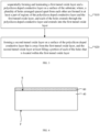
- FIG. 1 is a schematic view of a solar cell according to an embodiment of the present application.
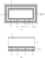
- FIG. 2 is a schematic view of a solar cell according to another embodiment of the present application.
- a first aspect of embodiments of the present application provides a solar cell 200.
- the solar cell 200 includes a substrate 40 and a passivated contact structure 100.
- the passivated contact structure 100 includes a first tunnel oxide layer 10, a polysilicon doped conductive layer 30, and a second tunnel oxide layer 20 that are sequentially disposed on a surface of the substrate 40.
- a plurality of holes 50 arranged spaced apart from each other are formed in at least a part of the regions of the polysilicon doped conductive layer 30 and the first tunnel oxide layer 10.
- Each of the holes 50 extends through the polysilicon doped conductive layer 30 and extends into the first tunnel oxide layer 10.
- the second tunnel oxide layer 20 at least fills the portion of each of the holes 50 that is located within the first tunnel oxide layer 10.
- the second tunnel oxide layer 20 is disposed, and the second tunnel oxide layer 20 at least fills the portion of each of the holes 50 that is located within the first tunnel oxide layer 10.
- the regions, that is, the discontinuous regions, of the first tunnel oxide layer 10 corresponding to the holes 50 can be filled with the second tunnel oxide layer 20, and regions on the surface of the substrate 40 corresponding to the holes 50 can also be covered by the second tunnel oxide layer 20.
- the solution of the present application can improve the quality of surface passivation, reduce surface recombination, and improve the conversion efficiency of the solar cell 200.
- the first tunnel oxide layer 10, the polysilicon doped conductive layer 30, and the second tunnel oxide layer 20 being sequentially disposed on the surface of the substrate 40 means that the first tunnel oxide layer 10 is disposed on a surface of the substrate 40, the polysilicon doped conductive layer 30 is disposed on a surface of the first tunnel oxide layer 10 facing away from the substrate 40, and the second tunnel oxide layer 20 is disposed on a surface of the polysilicon doped conductive layer 30 facing away from the first tunnel oxide layer 10.
- silicon substrate flaws and discontinuous portions in the first tunnel oxide layer 10 caused by the holes 50 can be filled with a part of the material of the second tunnel oxide layer 20.
- the positions of the plurality of holes 50 on the polysilicon doped conductive layer 30 and the first tunnel oxide layer 10 are randomly arranged, and for example, may be distributed within a local region, or may be distributed throughout the entire arrangement range of the polysilicon doped conductive layer 30 and the first tunnel oxide layer 10.
- Each of the holes 50 may include a first hole segment located within the polysilicon doped conductive layer 30 and a second hole segment located within the first tunnel oxide layer 10.
- the second tunnel oxide layer 20 at least filling the portion of each of the holes 50 that is located within the first tunnel oxide layer 10 means that, among all the holes 50, the second hole segments thereof located within the first tunnel oxide layer 10 are covered by the second tunnel oxide layer 20.
- the material of the second tunnel oxide layer 20 filled in each of the holes 50 needs to completely cover the second hole segments of the holes 50 that are located within the first tunnel oxide layer 10. Based on this, a part of the material of the second tunnel oxide layer 20 may further fill the first hole segments of the holes 50 that are located within the polysilicon doped conductive layer 30.
- the second tunnel oxide layer 20 fully fills each of the holes 50. In this way, the second tunnel oxide layer 20 can also form a film layer with relatively good integrity and continuity, and the portions of the substrate 40 corresponding to the holes 50 can have a better passivation effect.
- the holes 50 extends through the first tunnel oxide layer 10.
- the surface of the substrate 40 is partially exposed via the holes 50. Since the second tunnel oxide layer 20 fully fills the holes 50, the second tunnel oxide layer 20 can directly get in contact with the portions of the substrate 40 corresponding to the holes 50, thereby greatly enhancing the passivation effect at these portions.
- a cross-sectional profile of the hole 50 is in a circular shape, and a diameter of the hole 50 is greater than or equal to 100 nm.
- a cross-sectional profile of the hole 50 is in a shape of polygon, and a length of at least one edge of the polygon is greater than or equal to 100 nm.
- the polysilicon doped conductive layer 30 has a discontinuous structure. It may be understood that said polygon herein may be a regular or irregular polygon.
- a thickness of the first tunnel oxide layer 10 is equal to a thickness of the second tunnel oxide layer 20. And/or, the first tunnel oxide layer 10 is made of the same material as the second tunnel oxide layer 20.
- the thickness of the first tunnel oxide layer 10 is equal to the thickness of the second tunnel oxide layer 20, it can be ensured that when the second tunnel oxide layer 20 fills the holes 50, the second tunnel oxide layer 20at least fully fills the second hole segments of the holes 50 that are located within the first tunnel oxide layer 10.
- the second hole segment of each of the holes 50 that is located within the first tunnel oxide layer 10 is filled with a part of the material of the second tunnel oxide layer 20.
- the first tunnel oxide layer 10 and the second tunnel oxide layer 20 have the same thickness range, and made of the same material, so that both the first tunnel oxide layer 10 and the second tunnel oxide layer 20 can form an ultra-thin oxide layer, and uniformity and consistency of performance among positions of the first tunnel oxide layer 10 can be ensured.
- the first tunnel oxide layer 10 and the second tunnel oxide layer 20 may be made of dielectric materials, for example, the dielectric materials may be at least one of silicon oxide, silicon carbide, silicon nitride, or silicon oxynitride.
- the thickness of the second tunnel oxide layer 20 is in a range from 0.5 nm to 5 nm, and the thickness of the first tunnel oxide layer 10 may also be in a range from 0.5 nm to 5 nm.
- the polysilicon doped conductive layer 30 in order to reduce an impact of a dopant on the first tunnel oxide layer 10 in a process of forming the polysilicon doped conductive layer 30, it is considered that the polysilicon doped conductive layer 30 is configured to have a multi-layer structure, and that a part of the layer structure of the polysilicon doped conductive layer 30 adjacent to the first tunnel oxide layer 10 is configured to have a lower doping concentration.
- the polysilicon doped conductive layer 30 includes a first polysilicon doped conductive layer 31 and a second polysilicon doped conductive layer 32 that are laminated.
- the first polysilicon doped conductive layer 31 is adjacent to the first tunnel oxide layer 10, and the second polysilicon doped conductive layer 32 is adjacent to the second tunnel oxide layer 20.
- a doping concentration of the first polysilicon doped conductive layer 31 is lower than a doping concentration of the second polysilicon doped conductive layer 32.
- the first polysilicon doped conductive layer 31 with a relatively low doping concentration can have a higher hydrogen content, thereby assisting the first tunnel oxide layer 10 to achieve better surface passivation.
- the first polysilicon doped conductive layer 31 may also include a plurality of polysilicon doped sub-layers (not shown).
- the plurality of polysilicon doped sub-layers are laminated sequentially along a direction from the substrate 40 to the second tunnel oxide layer 20, with the doping concentrations increasing sequentially along such direction.
- the substrate 40 may include a first surface F and a second surface S that are opposite to each other, and may further include a plurality of side surfaces adjacent to and located between the first surface F and the second surface S.
- the first surface F may correspond to a back surface or a front surface of the solar cell 200.
- the second surface S may correspond to a front surface or a back surface of the solar cell 200.
- an example in which the first surface F corresponds to a back surface of the solar cell 200, and the first tunnel oxide layer 10 is disposed on the first surface F of the substrate 40 is used for description.
- a reflectivity of the first surface F of the substrate 40 is greater than 30%.
- the reflectivity thereof is 38%, 40%, 42%, or 45%.
- a roughness of the first surface F of the substrate 40 is less than 1 ⁇ m.
- the first surface F of the substrate 40 may be configured as a polished surface, so that the first surface F of the substrate 40 can have fewer silicon substrate flaws, thereby easily obtaining a better surface passivation effect.
- the solar cell 200 further includes a first passivation film layer 70, a doped conductive layer 60, a second passivation film layer 80, a first electrode 91, and a second electrode 92.
- the first passivation film layer 70 is laminated on a surface of the second tunnel oxide layer 20 that is away from the substrate 40.
- the first passivation film layer 70 may adopt a single-layer or multi-layer structure.
- the first passivation film layer 70 may be made of silicon oxide, silicon nitride, or silicon oxynitride. With development of the technology of the solar cell 200, the back surface of the solar cell 200 may also receive energy of solar light, which is mainly reflected light or scattered light in the surrounding environment.
- the first passivation film layer 70 may include, for example, at least one first anti-reflection layer (not shown).
- the doped conductive layer 60 and the second passivation film layer 80 are sequentially laminated on a surface of the substrate 40 that is away from the first tunnel oxide layer 10.
- the solar cell 200 may include an N type cell or a P type cell.
- the N type cell includes the substrate 40 doped with an N type element, and the doped conductive layer 60 doped with a P type element.
- the P type cell includes the substrate 40 doped with an P type element, and the doped conductive layer 60 doped with an N type element.
- the doped conductive layer 60 is configured to form a PN junction with the substrate 40.
- the doped conductive layer 60 may be P type doped, for example, may be a doped conductive layer 60 doped with a boron element.
- the doped conductive layer 60 doped with the boron element is also referred to as a P+ type emitter.
- the second passivation film layer 80 is laminated on the doped conductive layer 60.
- the second passivation film layer 80 plays roles in surface passivation and anti-reflection in the solar cell 200. Therefore, dangling bonds on the surface of the substrate 40 can be better chemically passivated, and an anti-reflection effect can be achieved on a front surface of the solar cell 200.
- the second passivation film layer 80 may include a second passivation layer (not shown) and a second anti-reflection layer (not shown) that are sequentially laminated on the doped conductive layer 60.
- the second anti-reflection layer is located on the second surface S of the substrate 40, that is, on a surface on which the solar cell 200 receives incident light.
- the surface on which the solar cell 200 receives incident light is also referred to as a front surface or a light receiving surface.
- the second anti-reflection layer plays an anti-reflection effect on the front surface of the solar cell 200.
- the second anti-reflection layer may adopt a multi-layer structure. In the second anti-reflection layer of the multi-layer structure, each of the layers may be made of silicon oxide, silicon nitride, or silicon oxynitride.
- the second passivation layer may adopt a single-layer structure or a multi-layer structure.
- the second passivation layer may be made of at least one of aluminium oxide, silicon oxide, silicon nitride, or silicon oxynitride.
- the second passivation layer may be formed by chemical deposition.
- first electrode 91 is disposed on the first passivation film layer 70, and is connected to the polysilicon doped conductive layer 30.
- the second electrode 92 is disposed on the second passivation film layer 80, and is connected to the doped conductive layer 60.
- FIG. 3 is a flow chart of a manufacturing method of a solar cell according to an embodiment of the present application.
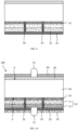
- FIG. 4 is a schematic view of a substrate of which a first surface is etched in the manufacturing method of the solar cell according to an embodiment of the present application.
- FIG. 5 is a schematic view of a first tunnel oxide material layer, a polysilicon doped conductive material layer, and a first oxide material layer formed on the first surface of the substrate in the manufacturing method of the solar cell according to an embodiment of the present application.
- FIG. 6 is a schematic view of a first tunnel oxide layer and a polysilicon doped conductive layer formed on the first surface F of the substrate in the manufacturing method of the solar cell according to an embodiment of the present application.
- FIG. 4 is a schematic view of a substrate of which a first surface is etched in the manufacturing method of the solar cell according to an embodiment of the present application.
- FIG. 5 is a schematic view of a first tunnel oxide material layer, a polysilicon doped conductive material layer
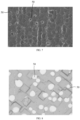
- FIG. 7 is a scanning electron microscopy photograph of holes formed in the manufacturing method of the solar cell according to an embodiment of the present application.
- FIG. 8 is a microscope image of holes formed in the manufacturing method of the solar cell according to an embodiment of the present application.
- FIG. 9 is a schematic view of a second tunnel oxide layer formed in the manufacturing method of the solar cell according to an embodiment of the present application.
- FIG. 10 is a schematic view of a solar cell formed in the manufacturing method of the solar cell according to an embodiment of the present application.
- a second aspect of embodiments of the present application provides a manufacturing method of a passivated contact structure.
- the solar cell 200 described in the foregoing embodiments can be manufactured by using this manufacturing method.
- the manufacturing method of the solar cell includes steps of S10 to S10.
- a first tunnel oxide layer 10 and a polysilicon doped conductive layer 30 are sequentially formed and laminated on a surface of a substrate 40.
- a plurality of holes 50 arranged spaced apart from each other are formed in at least a part of regions of the polysilicon doped conductive layer 30 and the first tunnel oxide layer 10. Each of the holes 50 extends through the polysilicon doped conductive layer 30 and extends into the first tunnel oxide layer 10.
- a second tunnel oxide layer 20 is formed on a surface of the polysilicon doped conductive layer 30 that is away from the first tunnel oxide layer 10, and the second tunnel oxide layer 20 at least fills a portion of each of the holes 50 that is located within the first tunnel oxide layer 10.
- the second tunnel oxide layer 20 is formed on the surface of the polysilicon doped conductive layer 30 that is away from the first tunnel oxide layer 10, and the second tunnel oxide layer 20 at least fills the portion of each of the holes 50 that is located within the first tunnel oxide layer 10.
- the regions of the surface of the substrate 40 and the first tunnel oxide layer 10 that correspond to the holes 50 can be covered by or filled with the second tunnel oxide layer 20.
- the solution of the present application can improve the quality of surface passivation, reduce surface recombination, and improve the conversion efficiency of the solar cell.
- the inventors of the present application had also tested the solution in which the second tunnel oxide layer 20 fills the holes 50. Compared with the solution in which the holes are not covered by the tunnel oxide layer, in the present application, the open circuit voltage Uoc is changed from 728 mV to 729 mV. It can be learned that the performance of the solar cell 200 manufactured by using the manufacturing method of the embodiments of the present application is improved to a certain extent.
- the step of sequentially forming and laminating the first tunnel oxide layer 10 and the polysilicon doped conductive layer 30 on the surface of the substrate 40 in step S10 specifically includes steps of S11 to S13.
- a first tunnel oxide material layer 11, a polysilicon doped material layer 301, and a first oxide material layer 302 are sequentially formed on a first surface F of the substrate 40.
- a plurality of through holes 303 are formed in the polysilicon doped material layer 301 and the first oxide material layer 302, such that regions of the first tunnel oxide material layer 11 corresponding to the through holes 303 are exposed, as shown in FIG. 5 .
- the first tunnel oxide material layer 11, the polysilicon doped material layer 301, and the first oxide material layer 302 that are plated around the second surface S of the substrate 40 and each of the side surfaces of the substrate 40 are removed, to sequentially form the first tunnel oxide layer 10, the polysilicon doped conductive layer 30, and a first oxide layer 305 on the first surface F of the substrate 40.
- the first oxide layer 305 is removed, and at least a part of regions of the first tunnel oxide layer 10 corresponding to the through holes 303 in a thickness direction of the first tunnel oxide material layer 11 is removed, so as to define the holes 50 together with the corresponding through holes 303.
- step S11 specifically includes steps of S111 to S112.
- a first tunnel oxide material layer 11 an amorphous silicon doped material layer 304, and a first oxide material layer 302 are sequentially formed on the first surface F of the substrate 40.
- an annealing process is performed to transform the amorphous silicon doped material layer 304 into the polysilicon doped material layer 301.
- the plurality of through holes 303 are formed in the polysilicon doped material layer 301 and the first oxide material layer 302.
- a process condition of the annealing process in step S112 includes:
- the first preset temperature may be in a range from 850°C to 990°C.
- the step of forming the amorphous silicon doped material layer 304 in step S111 includes: sequentially forming and laminating a first amorphous silicon material layer 3041 and a second amorphous silicon material layer 3042 on a surface of the first tunnel oxide material layer 11 that is away from the substrate 40, where an effective electroactive doping concentration of the first amorphous silicon material layer 3041 is less than an effective electroactive doping concentration of the second amorphous silicon material layer 3042.
- the first amorphous silicon material layer 3041 can alleviate the impact on the first tunnel oxide layer 10 brought by crystallizing the dopant in the second amorphous silicon material layer 3042 during high temperature annealing.
- the undoped or low-concentration doped first amorphous silicon material layer 3041 has a higher hydrogen content, and thus may provide more hydrogen, thereby assisting the first tunnel oxide layer 10 to achieve better surface passivation.
- the inventors of the present application have also tested the solution in which the polysilicon doped conductive layer 30 is formed by the first amorphous silicon material layer 3041 and the second amorphous silicon material layer 3042. Compared with a solution in which a single-layer polysilicon doped conductive layer is formed, in the present application, the open circuit voltage Uoc is changed from 727 mV to 729 mV. It can be learned that the performance of the solar cell 200 manufactured by using the manufacturing method of the embodiments of the present application is improved to a certain extent.
- the effective electroactive doping concentration of the first amorphous silicon material layer 3041 is less than 2E20cm -3
- the effective electroactive doping concentration of the second amorphous silicon material layer 3042 is greater than or equal to 2E20cm -3 .
- the effective electroactive doping concentration of the first amorphous silicon material layer 3041 may be 0, that is, the first amorphous silicon material layer 3041 may be an intrinsic amorphous silicon material layer.
- the removing the first oxide layer 305 and removing at least a part of regions of the first tunnel oxide layer 10 corresponding to the through holes 303 in a thickness direction of the first tunnel oxide layer 10, so as to define the holes 50 together with the corresponding through holes 303 in step S13, in a specific implementation, it can be implemented by washing with an acid solution including HF.
- an acid solution including HF it can be implemented by washing with an acid solution including HF.
- the step of forming the second tunnel oxide layer 20 on the surface of the polysilicon doped conductive layer 30 that is away from the first tunnel oxide layer 10 in step S20 includes: forming the second tunnel oxide layer 20 on the surface of the polysilicon doped conductive layer 30 that is away from the first tunnel oxide layer 10, and the second tunnel oxide layer 20 fully filling the holes 50.
- the manufacturing method further includes: before the step of sequentially forming and laminating the first tunnel oxide layer 10 and the polysilicon doped conductive layer 30 on the surface of the substrate 40 in step S10, performing etching processing on the first surface F of the substrate 40, such that a reflectivity of the first surface F is greater than 30%, and/or, performing etching processing on the first surface F of the substrate 40, such that a roughness of the first surface F of the substrate 40 is less than 1 ⁇ m; where the first surface F is a surface of the substrate 40 on which the first tunnel oxide layer 10 is to be formed.
- the first surface F of the substrate 40 can have fewer silicon substrate flaws, thereby easily obtaining a better surface passivation effect.
- the step of performing etching processing on the first surface F of the substrate 40 includes: forming a doped conductive material layer on the second surface S of the substrate 40.
- the doped conductive layer is P-type and doped with a boron element, for example, the doped conductive material layer may be formed by performing boron diffusion on the second surface S of the substrate 40.
- the doped conductive material layer plated around each of the side surfaces and the first surface F of the substrate 40 is removed by etching, to form a doped conductive layer 60 on the second surface S of the substrate 40, as shown in FIG. 4 .
- the doped conductive layer 60 herein is configured to form a PN junction with the substrate 40, and a doping type of the doped conductive layer 60 is opposite to that of the polysilicon doped conductive layer 30.
- the manufacturing method further includes: after the step of forming the second tunnel oxide layer 20 on the surface of the polysilicon doped conductive layer 30 that is away from the first tunnel oxide layer 10 in step S20,
- the manufacturing method includes step 1 to step 7:
- the step of forming the first tunnel oxide material layer 11 includes: introducing an oxygen source at a temperature of 300°C or higher.
- the oxygen source may be, for example, N 2 O, CO, CO 2 , or the like.
- the oxygen source is ionized under a microwave power supply to generate oxygen ions.
- the oxygen ions react with the surface of the substrate 40 to form an ultra-thin first tunnel oxide material layer 11, which have a thickness in a range from 0.5 nm to 5 nm.
- the step of forming the first amorphous silicon material layer 3041 includes: introducing silane and hydrogen in a first ratio, or silane and argon in a first ratio; and depositing and growing a hydrogen-rich intrinsic amorphous silicon layer as the first amorphous silicon material layer 3041 under the action of a microwave power supply.
- silane, phosphane and hydrogen in a first ratio are introduced, or silane, phosphoane and argon in a first ratio are introduced, and under the action of the microwave power supply, a hydrogen-rich lightly doped amorphous silicon layer is deposited and grew as the first amorphous silicon material layer 3041.
- the step of forming the second amorphous silicon material layer 3042 includes: introducing silane and phosphane in a second ratio different from the first ration, in which the ratio of phosphane to silane is greater than that of the first amorphous silicon material layer 3041, and depositing and growing a doped amorphous silicon layer with a higher doping concentration as the second amorphous silicon material layer 3042.
- Step 4 at a temperature of 800°C or higher, annealing processing is performed on the structure body formed in Step 3, such that the first tunnel oxide material layer 11, the first amorphous silicon material layer 3041, and the second amorphous silicon material layer 3042 are crystallized, and transformed into a polysilicon doped material layer 301, that is, a first polysilicon doped material layer and a second polysilicon doped material layer.
- a polysilicon doped material layer 301 that is, a first polysilicon doped material layer and a second polysilicon doped material layer.
- an excess part of hydrogen on the surface of the first tunnel oxide material layer 11 escapes, forming through holes 303 each having a size of 100 nm or larger in the polysilicon doped material layer 301 and the first oxide material layer 302.
- regions of the first tunnel oxide material layer 11 corresponding to the through holes 303 are exposed, thereby forming a structure shown in FIG. 5 .
- the first tunnel oxide material layer 11, the polysilicon doped material layer 301, and the first oxide material layer 302 that are plated around the second surface S of the substrate 40 and each of the side surfaces of the substrate 40 are removed, to sequentially form the first tunnel oxide layer 10, the polysilicon doped conductive layer 30 (that is, a first polysilicon doped conductive layer 31 and a second polysilicon doped conductive layer 32), and the first oxide layer 305 on the first surface F of the substrate 40.
- the first oxide layer 305 is removed, and at least a part of regions of the first tunnel oxide layer 10 corresponding to the through holes 303 is removed in the thickness direction of the first tunnel oxide layer 10, so as to define the holes 50 together with the corresponding through holes 303.
- the obtained structure body is shown in FIG. 6 , and the structures of the holes 50 are shown in FIGS. 7 and 8 .
- a second tunnel oxide layer 20 is formed on the polysilicon doped conductive layer 30 by using plasma enhanced chemical vapor deposition (PECVD).
- PECVD plasma enhanced chemical vapor deposition
- the second tunnel oxide layer 20 fills the holes 50.
- a range of thickness of the second tunnel oxide layer 20 is consistent with that of the first tunnel oxide layer 10, as shown in FIG. 9 .
- a second passivation film layer 80 is formed on a surface of the doped conductive layer 60 facing away from the substrate 40; a first passivation film layer 70 is formed on a surface of the second tunnel oxide layer 20 facing away from the substrate 40; and a first electrode 91 and a second electrode 92 are formed respectively on the first passivation film layer 70 and the second passivation film layer 80.
- the first passivation film layer 70 and the second passivation film layer 80 may be made of materials including aluminium oxide, silicon nitride, silicon oxynitride, silicon oxide, or the like.
- the solar cell 200 manufactured by using the manufacturing method of the embodiments of the present application since more hydrogen is supplied to passivate the surface of the substrate 40, a sufficient passivation effect can be achieved.
- the second tunnel oxide layer 20 is deposited on the surface of the polysilicon doped conductive layer 30 on which excessive hydrogen escapes.
- the polysilicon doped conductive layer 30 includes holes 50, which can improve and compensate for surface passivation quality. Compared with a hole-free structure, in the present application, the surface passivation quality can be improved, the surface recombination can be reduced, and the conversion efficiency of the solar cell 200 can be improved.
- a third aspect of embodiments of the present application provides a photovoltaic module (not shown in the figure).
- the photovoltaic module includes at least one cell string.
- the cell string includes at least two solar cells 200 described above.
- the solar cells 200 may be connected together by series welding.
- a fourth aspect of embodiments of the present application provides a photovoltaic system (not shown).
- the photovoltaic system includes the foregoing photovoltaic module.
- the photovoltaic system may be applied to a photovoltaic power station, such as a ground-mounted power station, a roof-mounted power station, a water-on-power station, or the like, or may be applied to a device or an apparatus that generates power by using solar energy, such as a user solar power supply, a solar street lamp, a solar vehicle, a solar building, or the like.
- a photovoltaic power station such as a ground-mounted power station, a roof-mounted power station, a water-on-power station, or the like
- a device or an apparatus that generates power by using solar energy such as a user solar power supply, a solar street lamp, a solar vehicle, a solar building, or the like.
- the photovoltaic system may be applied to all fields in which solar energy needs to be used for generating power.
- the photovoltaic system may include photovoltaic arrays, combiner boxes, and inverters.
- the photovoltaic array may be an array combination of a plurality of photovoltaic modules.
- the plurality of photovoltaic modules may form a plurality of photovoltaic arrays.
- the photovoltaic arrays are connected to combiner boxes.
- the combiner boxes may combine the current generated by the photovoltaic arrays.
- the combined current flows through the inverters and is converted into an alternating current required by a mains power network, and is then input to the mains power network to implement solar power supply.
Landscapes
- Photovoltaic Devices (AREA)
- Chemical & Material Sciences (AREA)
- Crystallography & Structural Chemistry (AREA)
- Life Sciences & Earth Sciences (AREA)
- Engineering & Computer Science (AREA)
- Sustainable Development (AREA)
- Sustainable Energy (AREA)
Applications Claiming Priority (1)
| Application Number | Priority Date | Filing Date | Title |
|---|---|---|---|
| CN202311561364.2A CN117276361B (zh) | 2023-11-22 | 2023-11-22 | 太阳能电池及其制作方法、光伏组件及光伏系统 |
Publications (2)
| Publication Number | Publication Date |
|---|---|
| EP4401153A2 true EP4401153A2 (de) | 2024-07-17 |
| EP4401153A3 EP4401153A3 (de) | 2025-01-22 |
Family
ID=89219977
Family Applications (1)
| Application Number | Title | Priority Date | Filing Date |
|---|---|---|---|
| EP24178575.7A Pending EP4401153A3 (de) | 2023-11-22 | 2024-05-28 | Solarzelle und herstellungsverfahren dafür, fotovoltaisches modul und fotovoltaisches system |
Country Status (5)
| Country | Link |
|---|---|
| US (1) | US20240355940A1 (de) |
| EP (1) | EP4401153A3 (de) |
| JP (1) | JP7713561B2 (de) |
| CN (1) | CN117276361B (de) |
| AU (2) | AU2024203444B2 (de) |
Families Citing this family (2)
| Publication number | Priority date | Publication date | Assignee | Title |
|---|---|---|---|---|
| CN117766598B (zh) * | 2023-12-27 | 2024-10-25 | 天合光能股份有限公司 | 光伏电池、光伏电池组件与光伏电池的制造方法 |
| CN120730879B (zh) * | 2025-08-29 | 2025-11-25 | 晶科能源(海宁)有限公司 | 光伏电池及其制备方法、光伏组件 |
Family Cites Families (17)
| Publication number | Priority date | Publication date | Assignee | Title |
|---|---|---|---|---|
| US10043934B2 (en) * | 2011-06-08 | 2018-08-07 | International Business Machines Corporation | Silicon-containing heterojunction photovoltaic element and device |
| KR101620431B1 (ko) * | 2014-01-29 | 2016-05-12 | 엘지전자 주식회사 | 태양 전지 및 이의 제조 방법 |
| KR101622091B1 (ko) | 2014-08-20 | 2016-05-18 | 엘지전자 주식회사 | 태양 전지 및 이의 제조 방법 |
| CN108074989A (zh) * | 2016-11-14 | 2018-05-25 | Lg电子株式会社 | 太阳能电池及其制造方法 |
| WO2020180244A1 (en) | 2019-03-01 | 2020-09-10 | National University Of Singapore | Solar cell and method for fabricating a solar cell |
| CN215183998U (zh) | 2021-04-23 | 2021-12-14 | 苏州腾晖光伏技术有限公司 | 一种基于钝化接触结构的mwt电池 |
| CN113299769B (zh) | 2021-06-04 | 2025-12-02 | 浙江爱旭太阳能科技有限公司 | 一种选择性接触区域掩埋型太阳能电池及其背面接触结构 |
| CN113594274A (zh) | 2021-08-30 | 2021-11-02 | 浙江爱旭太阳能科技有限公司 | 一种太阳能电池及其接触结构、电池组件及光伏系统 |
| CN113838941B (zh) | 2021-11-23 | 2022-02-11 | 浙江爱旭太阳能科技有限公司 | 一种太阳能电池的选择性钝化接触结构和双面太阳能电池 |
| CN115101604A (zh) * | 2022-06-23 | 2022-09-23 | 浙江爱旭太阳能科技有限公司 | TOPCon太阳能电池片及其制备方法、电池组件和光伏系统 |
| CN219917178U (zh) * | 2022-12-19 | 2023-10-27 | 浙江爱旭太阳能科技有限公司 | 一种晶格钝化接触结构、太阳能电池、组件和系统 |
| CN115863452A (zh) * | 2023-01-03 | 2023-03-28 | 晶科能源(海宁)有限公司 | 太阳能电池及其制备方法、光伏组件 |
| CN116093207A (zh) * | 2023-03-02 | 2023-05-09 | 正泰新能科技有限公司 | 一种背接触太阳能电池及其制作方法 |
| CN219371038U (zh) * | 2023-03-16 | 2023-07-18 | 韩华新能源(启东)有限公司 | 一种太阳能电池背面结构及n-tbc背接触太阳能电池 |
| CN116314361B (zh) * | 2023-03-31 | 2025-06-13 | 天合光能股份有限公司 | 太阳电池及太阳电池的制备方法 |
| CN116914027A (zh) * | 2023-08-11 | 2023-10-20 | 天合光能股份有限公司 | 背接触式太阳能电池及制作方法、光伏组件及制作方法 |
| CN116885019A (zh) * | 2023-08-15 | 2023-10-13 | 江西沐邦高科股份有限公司 | 一种太阳能电池及其制备方法 |
-
2023
- 2023-11-22 CN CN202311561364.2A patent/CN117276361B/zh active Active
-
2024
- 2024-05-23 AU AU2024203444A patent/AU2024203444B2/en active Active
- 2024-05-28 EP EP24178575.7A patent/EP4401153A3/de active Pending
- 2024-06-06 JP JP2024092427A patent/JP7713561B2/ja active Active
- 2024-06-28 US US18/757,693 patent/US20240355940A1/en active Pending
-
2025
- 2025-02-06 AU AU2025200820A patent/AU2025200820A1/en active Pending
Also Published As
| Publication number | Publication date |
|---|---|
| US20240355940A1 (en) | 2024-10-24 |
| JP7713561B2 (ja) | 2025-07-25 |
| AU2024203444A1 (en) | 2024-06-13 |
| AU2024203444B2 (en) | 2024-11-28 |
| EP4401153A3 (de) | 2025-01-22 |
| AU2025200820A1 (en) | 2025-02-27 |
| JP2024113117A (ja) | 2024-08-21 |
| CN117276361A (zh) | 2023-12-22 |
| CN117276361B (zh) | 2024-02-02 |
Similar Documents
| Publication | Publication Date | Title |
|---|---|---|
| CN115241298B (zh) | 太阳能电池及其制备方法、光伏组件 | |
| JP2024509329A (ja) | 選択的接触領域埋込型太陽電池及びその裏面接触構造 | |
| EP4401153A2 (de) | Solarzelle, herstellungsverfahren dafür, fotovoltaisches modul und photovoltaiksystem | |
| US20250301820A1 (en) | Solar cell, method for manufacturing the same, photovoltaic module and photovoltaic system | |
| JP2009164544A (ja) | 太陽電池のパッシベーション層構造およびその製造方法 | |
| NL2034327A (en) | Solar cell and manufacture method thereof, and photovoltaic module | |
| JP2024155726A (ja) | 太陽電池およびその製造方法、光起電力モジュール | |
| JP2024511224A (ja) | 選択的接触領域埋込型太陽電池及びその裏面接触構造 | |
| US20160284917A1 (en) | Passivation Layer for Solar Cells | |
| US20250169221A1 (en) | Solar cell, photovoltaic module, and photovoltaic system | |
| CN117650188B (zh) | 太阳电池及其制备方法、光伏组件、光伏系统 | |
| EP4425573A2 (de) | Solarzelle und herstellungsverfahren dafür, fotovoltaisches modul und fotovoltaiksystem | |
| CN116110978A (zh) | 太阳能电池及其制备方法、光伏组件 | |
| CN119836046B (zh) | 一种太阳能电池及太阳能电池的制备方法 | |
| KR20160061409A (ko) | 태양 전지를 생성하는 방법 | |
| KR20160138183A (ko) | 태양 전지의 수광 표면의 패시베이션 | |
| JP2675754B2 (ja) | 太陽電池 | |
| CN119170665A (zh) | 太阳能电池及其制作方法、光伏组件 | |
| CN119069548A (zh) | 太阳能电池及其制备方法、光伏组件 | |
| CN222692235U (zh) | 太阳能电池、光伏组件及光伏系统 | |
| CN119730399A (zh) | 太阳能电池、太阳能电池的制作方法和光伏组件 | |
| CN119364865A (zh) | 太阳能电池及其制备方法、光伏组件 | |
| CN120035260A (zh) | 太阳能电池的制备方法、太阳能电池和光伏组件 | |
| CN119230661A (zh) | 太阳能电池及其制备方法 | |
| CN120640809A (zh) | 背接触电池及其制备方法 |
Legal Events
| Date | Code | Title | Description |
|---|---|---|---|
| PUAI | Public reference made under article 153(3) epc to a published international application that has entered the european phase |
Free format text: ORIGINAL CODE: 0009012 |
|
| STAA | Information on the status of an ep patent application or granted ep patent |
Free format text: STATUS: REQUEST FOR EXAMINATION WAS MADE |
|
| 17P | Request for examination filed |
Effective date: 20240528 |
|
| AK | Designated contracting states |
Kind code of ref document: A2 Designated state(s): AL AT BE BG CH CY CZ DE DK EE ES FI FR GB GR HR HU IE IS IT LI LT LU LV MC ME MK MT NL NO PL PT RO RS SE SI SK SM TR |
|
| PUAL | Search report despatched |
Free format text: ORIGINAL CODE: 0009013 |
|
| AK | Designated contracting states |
Kind code of ref document: A3 Designated state(s): AL AT BE BG CH CY CZ DE DK EE ES FI FR GB GR HR HU IE IS IT LI LT LU LV MC ME MK MT NL NO PL PT RO RS SE SI SK SM TR |
|
| RIC1 | Information provided on ipc code assigned before grant |
Ipc: H01L 31/0216 20140101ALI20241216BHEP Ipc: H01L 31/0747 20120101ALI20241216BHEP Ipc: H01L 31/068 20120101AFI20241216BHEP |