EP4398232A1 - Bildschirmansteuerungsschaltung, anzeigebildschirm und elektronische vorrichtung - Google Patents
Bildschirmansteuerungsschaltung, anzeigebildschirm und elektronische vorrichtung Download PDFInfo
- Publication number
- EP4398232A1 EP4398232A1 EP23799162.5A EP23799162A EP4398232A1 EP 4398232 A1 EP4398232 A1 EP 4398232A1 EP 23799162 A EP23799162 A EP 23799162A EP 4398232 A1 EP4398232 A1 EP 4398232A1
- Authority
- EP
- European Patent Office
- Prior art keywords
- switching transistor
- terminal
- signal
- drive
- drive circuit
- Prior art date
- Legal status (The legal status is an assumption and is not a legal conclusion. Google has not performed a legal analysis and makes no representation as to the accuracy of the status listed.)
- Pending
Links
Images


Classifications
-
- G—PHYSICS
- G09—EDUCATION; CRYPTOGRAPHY; DISPLAY; ADVERTISING; SEALS
- G09G—ARRANGEMENTS OR CIRCUITS FOR CONTROL OF INDICATING DEVICES USING STATIC MEANS TO PRESENT VARIABLE INFORMATION
- G09G3/00—Control arrangements or circuits, of interest only in connection with visual indicators other than cathode-ray tubes
- G09G3/20—Control arrangements or circuits, of interest only in connection with visual indicators other than cathode-ray tubes for presentation of an assembly of a number of characters, e.g. a page, by composing the assembly by combination of individual elements arranged in a matrix no fixed position being assigned to or needed to be assigned to the individual characters or partial characters
- G09G3/22—Control arrangements or circuits, of interest only in connection with visual indicators other than cathode-ray tubes for presentation of an assembly of a number of characters, e.g. a page, by composing the assembly by combination of individual elements arranged in a matrix no fixed position being assigned to or needed to be assigned to the individual characters or partial characters using controlled light sources
- G09G3/30—Control arrangements or circuits, of interest only in connection with visual indicators other than cathode-ray tubes for presentation of an assembly of a number of characters, e.g. a page, by composing the assembly by combination of individual elements arranged in a matrix no fixed position being assigned to or needed to be assigned to the individual characters or partial characters using controlled light sources using electroluminescent panels
- G09G3/32—Control arrangements or circuits, of interest only in connection with visual indicators other than cathode-ray tubes for presentation of an assembly of a number of characters, e.g. a page, by composing the assembly by combination of individual elements arranged in a matrix no fixed position being assigned to or needed to be assigned to the individual characters or partial characters using controlled light sources using electroluminescent panels semiconductive, e.g. using light-emitting diodes [LED]
- G09G3/3208—Control arrangements or circuits, of interest only in connection with visual indicators other than cathode-ray tubes for presentation of an assembly of a number of characters, e.g. a page, by composing the assembly by combination of individual elements arranged in a matrix no fixed position being assigned to or needed to be assigned to the individual characters or partial characters using controlled light sources using electroluminescent panels semiconductive, e.g. using light-emitting diodes [LED] organic, e.g. using organic light-emitting diodes [OLED]
- G09G3/3266—Details of drivers for scan electrodes
-
- G—PHYSICS
- G09—EDUCATION; CRYPTOGRAPHY; DISPLAY; ADVERTISING; SEALS
- G09G—ARRANGEMENTS OR CIRCUITS FOR CONTROL OF INDICATING DEVICES USING STATIC MEANS TO PRESENT VARIABLE INFORMATION
- G09G3/00—Control arrangements or circuits, of interest only in connection with visual indicators other than cathode-ray tubes
- G09G3/20—Control arrangements or circuits, of interest only in connection with visual indicators other than cathode-ray tubes for presentation of an assembly of a number of characters, e.g. a page, by composing the assembly by combination of individual elements arranged in a matrix no fixed position being assigned to or needed to be assigned to the individual characters or partial characters
- G09G3/22—Control arrangements or circuits, of interest only in connection with visual indicators other than cathode-ray tubes for presentation of an assembly of a number of characters, e.g. a page, by composing the assembly by combination of individual elements arranged in a matrix no fixed position being assigned to or needed to be assigned to the individual characters or partial characters using controlled light sources
- G09G3/30—Control arrangements or circuits, of interest only in connection with visual indicators other than cathode-ray tubes for presentation of an assembly of a number of characters, e.g. a page, by composing the assembly by combination of individual elements arranged in a matrix no fixed position being assigned to or needed to be assigned to the individual characters or partial characters using controlled light sources using electroluminescent panels
- G09G3/32—Control arrangements or circuits, of interest only in connection with visual indicators other than cathode-ray tubes for presentation of an assembly of a number of characters, e.g. a page, by composing the assembly by combination of individual elements arranged in a matrix no fixed position being assigned to or needed to be assigned to the individual characters or partial characters using controlled light sources using electroluminescent panels semiconductive, e.g. using light-emitting diodes [LED]
- G09G3/3208—Control arrangements or circuits, of interest only in connection with visual indicators other than cathode-ray tubes for presentation of an assembly of a number of characters, e.g. a page, by composing the assembly by combination of individual elements arranged in a matrix no fixed position being assigned to or needed to be assigned to the individual characters or partial characters using controlled light sources using electroluminescent panels semiconductive, e.g. using light-emitting diodes [LED] organic, e.g. using organic light-emitting diodes [OLED]
- G09G3/3225—Control arrangements or circuits, of interest only in connection with visual indicators other than cathode-ray tubes for presentation of an assembly of a number of characters, e.g. a page, by composing the assembly by combination of individual elements arranged in a matrix no fixed position being assigned to or needed to be assigned to the individual characters or partial characters using controlled light sources using electroluminescent panels semiconductive, e.g. using light-emitting diodes [LED] organic, e.g. using organic light-emitting diodes [OLED] using an active matrix
-
- G—PHYSICS
- G09—EDUCATION; CRYPTOGRAPHY; DISPLAY; ADVERTISING; SEALS
- G09G—ARRANGEMENTS OR CIRCUITS FOR CONTROL OF INDICATING DEVICES USING STATIC MEANS TO PRESENT VARIABLE INFORMATION
- G09G3/00—Control arrangements or circuits, of interest only in connection with visual indicators other than cathode-ray tubes
- G09G3/20—Control arrangements or circuits, of interest only in connection with visual indicators other than cathode-ray tubes for presentation of an assembly of a number of characters, e.g. a page, by composing the assembly by combination of individual elements arranged in a matrix no fixed position being assigned to or needed to be assigned to the individual characters or partial characters
- G09G3/34—Control arrangements or circuits, of interest only in connection with visual indicators other than cathode-ray tubes for presentation of an assembly of a number of characters, e.g. a page, by composing the assembly by combination of individual elements arranged in a matrix no fixed position being assigned to or needed to be assigned to the individual characters or partial characters by control of light from an independent source
- G09G3/36—Control arrangements or circuits, of interest only in connection with visual indicators other than cathode-ray tubes for presentation of an assembly of a number of characters, e.g. a page, by composing the assembly by combination of individual elements arranged in a matrix no fixed position being assigned to or needed to be assigned to the individual characters or partial characters by control of light from an independent source using liquid crystals
-
- G—PHYSICS
- G09—EDUCATION; CRYPTOGRAPHY; DISPLAY; ADVERTISING; SEALS
- G09G—ARRANGEMENTS OR CIRCUITS FOR CONTROL OF INDICATING DEVICES USING STATIC MEANS TO PRESENT VARIABLE INFORMATION
- G09G2310/00—Command of the display device
- G09G2310/04—Partial updating of the display screen
-
- G—PHYSICS
- G09—EDUCATION; CRYPTOGRAPHY; DISPLAY; ADVERTISING; SEALS
- G09G—ARRANGEMENTS OR CIRCUITS FOR CONTROL OF INDICATING DEVICES USING STATIC MEANS TO PRESENT VARIABLE INFORMATION
- G09G2330/00—Aspects of power supply; Aspects of display protection and defect management
- G09G2330/02—Details of power systems and of start or stop of display operation
- G09G2330/021—Power management, e.g. power saving
Definitions
- This application relates to the field of display technologies, and in particular, to a screen drive circuit, a display, and an electronic device.
- organic light-emitting diode organic light-emitting diode
- OLED organic light-emitting diode
- a data signal is linearly written under driving by a line scan signal (also referred to as GOA or a shift register), and is written by using a pixel signal on an entire screen, so as to implement content refreshing.
- GOA line scan signal
- global refreshing causes high power consumption and a long delay.
- this application provides a screen drive circuit, applied to a display and including an array drive circuit and a drive selection circuit.
- the array drive circuit includes a row drive circuit and a column drive circuit; the row drive circuit generates a row drive signal that is used to drive a pixel row in the display; and an input terminal of the drive selection circuit is connected to an output terminal of the row drive circuit, a control terminal of the drive selection circuit receives a row address selection signal to output, based on the row address selection signal, the row drive signal corresponding to a pixel row whose displayed content changes, and the row address selection signal is generated, by a display drive chip connected to the display, based on the pixel row whose displayed content changes.
- the drive selection circuit is configured to output the row drive signal when the row address selection signal is valid and mask the row drive signal when the row address selection signal is invalid.
- some pixel rows in a pixel array can be separately selected based on an update frequency of displayed content on the display for content refreshing, in other words, displayed content in a region whose content is to be updated can be refreshed by using the drive selection circuit, without refreshing displayed content in a picture holding region.
- the pixel array is an effective display region of an AMOLED display, and is configured to display content.
- a typical distribution of the pixel array is an array of 1920* 1080 pixels.
- Each pixel in the pixel array includes an RGB light-emitting diode, that is, an RGBOLED.
- the GOA circuit 100 is a row drive circuit of a row of pixels in a pixel array.
- An input terminal of the GOA circuit 100 is connected to an output terminal of the DDIC, and separately receives a start signal (STV) and two clock signals (CLK1 and CKB) that are sent by the DDIC, so as to receive a serial clock signal output by the DDIC, and write data to the pixel drive circuit based on a serial clock sequence, that is, output a write drive signal.
- STV start signal
- CLK1 and CKB two clock signals
- the drive selection circuit 200 may include a selection circuit 201 and a drive circuit 202.
- the selection circuit 201 includes an input terminal and a control terminal.
- the input terminal of the selection circuit 201 is the input terminal of the drive selection circuit 200
- the control terminal of the selection circuit 201 is the control terminal of the drive selection circuit 200, and is connected to the control signal output terminal of the DDIC.
- the drive circuit 202 converts the write pulse signal into a drive signal with a driving capability, and transmits the drive signal to a row of pixel circuit connected to the drive circuit 202, so that data is written to the corresponding pixel circuit based on a data signal provided by a column drive circuit, that is, displayed content of the pixel is refreshed.
- Q1 and Q2 are connected in series to obtain a first series branch
- Q3 and Q4 are connected in series to obtain a second series branch
- the first series branch is connected in parallel to the second series branch.
- a gate of Q 1 is the input terminal of the selection circuit 201, a second terminal of Q1 is connected to a second terminal of Q2, and a first terminal of Q1 is connected to a first terminal of Q3.
- the first terminal of Q1 is further connected to the input terminal of the drive circuit 202.
- a second terminal of Q3 is connected to a first terminal of Q4, a second terminal of Q4 is connected to a first terminal of Q2, and a common terminal of Q3 and Q4 inputs a negative voltage signal VgL (for example, -8 V).
- VgL negative voltage signal
- Gates of Q3 and Q4 are connected, and then are connected to the second terminal of Q4.
- a gate of Q2 inputs a first voltage signal V1.
- the first voltage signal V1 is a low-level signal, such as a 0 V voltage signal or a direct-current voltage.
- Q5 ⁇ Q7 form two stages of lock circuits.
- Q5 and Q6 are one stage of lock circuit, and Q7 and Q8 are the other stage of lock circuit.
- a first terminal of Q7 inputs the positive voltage signal VgH
- a second terminal of Q7 is connected to a first terminal of Q8, and a second terminal of Q8 inputs the negative voltage signal VgL.
- Gates of Q7 and Q8 input the control signal CLK2.
- the drive circuit 202 includes switching transistors Q9 and Q10.
- a first terminal of Q9 inputs the positive voltage signal VgH
- a second terminal of Q9 is connected to a first terminal of Q10
- a second terminal of Q10 inputs the negative voltage signal VgL.
- a drain-source common terminal of Q9 and Q10 (that is, a serially-connected node of Q9 and Q10) is the output terminal OUT of the drive circuit.
- Gates of Q9 and Q10 are the input terminal of the drive circuit 202, and are connected to the first terminal of Q1.
- Q9 and Q10 may be separately a switching transistor group obtained by connecting a plurality of switching transistors of a same type in parallel, and this application sets no limitation on a quantity of switching transistors connected in parallel.
- Q 1 may alternatively be an NMOS transistor, and another switching transistor in a corresponding circuit may be a semiconductor transistor of a corresponding type. This application sets no limitation thereto.
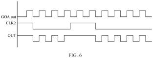
- FIG. 6 is a schematic diagram of waveforms of signals in a drive selection circuit according to an embodiment of this application.
- GOAout is an output signal of the GOA circuit
- CLK2 is a control signal output by the DDIC
- OUT is a signal output by the drive selection circuit 200.
- the drive selection circuit 200 transmits, to a pixel drive circuit at a subsequent stage, the write drive signal output by the GOA circuit 100, so as to drive a pixel of a corresponding row to refresh content. That is, a waveform of the OUT signal output by the drive selection circuit 200 is the same as a pulse signal waveform of GOA out.
- the write drive signal output by the GOA circuit 100 is masked, that is, the write drive signal corresponding to this row of pixels is masked. In other words, displayed content of this row of pixel circuit is not refreshed.
- the OUT signal output by the drive selection circuit 200 is also a high-level signal, that is, a write invalid signal.
- FIG. 7 is a diagram of a circuit principle corresponding to a drive selection circuit in a case that CLK2 is valid.
- CLK2 is valid at a low level is used as an example for description.
- CLK2 may be valid at a high level, and the drive selection circuit needs to be adaptively adjusted. Details are not described herein again.
- a type of a valid level of CLK2 is not limited in this application.
- Q3 and Q4 are in a high-resistance state, and Q1 and Q3 are equivalent to a resistor with a high resistance after being connected in series. Similarly, Q2 and Q4 are also equivalent to a resistor with a high resistance.
- a voltage difference between Q1 and Q3 is VgH-VgL.
- a pulse signal that is, the write drive signal
- a pulse signal at a same frequency is differentially output from point C, that is, the input terminal (that is, point D) of the drive circuit inputs the pulse signal.
- a pulse signal that has a same frequency as the pulse signal output from point C and that has a driving capability is output from the output terminal OUT. It can be learned that, when CLK2 is valid, the write drive signal output by the GOA circuit is output at the output terminal OUT. As shown in FIG.
- a signal finally output by the output terminal OUT of 200 is also a high-level signal, that is, an invalid signal.
- FIG. 9 is a schematic diagram of a plurality of row drive circuits according to an embodiment of this application.
- each row drive circuit includes one GOA circuit and one drive selection circuit.
- An output signal of each GOA circuit is a GOA out signal waveform, that is, all rows (S01-SN) of pixels need to refresh displayed content, and CLK2 is a control signal for row address selection. That CLK2 is valid at a low level is used as an example.
- an OUT signal finally output by each drive selection circuit includes only a row drive signal corresponding to a row whose displayed content is to be updated. For a row whose content is not to be updated, an invalid signal is output.
- the CLK2 signal is a control signal for row address selection, or is referred to as a row selection signal.
- a row drive signal corresponding to the row of pixels is output.
- a row drive signal corresponding to the row of pixels is masked. In coordination with address selection in a column direction, only displayed content of a partial display region of the screen is refreshed based on the displayed content.
- a 12* 10 pixel array is used as an example for description.
- An output terminal of each row of GOA circuit is connected to a drive selection circuit, an output buffer of the DDIC outputs a serial clock signal, and the DDIC generates a row address selection signal CLK2 based on a pixel row whose content is to be updated.
- Logical processing is performed on CLK2 and row drive signals output by N GOA circuits, and finally a corresponding row drive signal is output for only a row whose content is to be updated.
- a drive selection circuit For a CLK2-valid row, a drive selection circuit is on, that is, a corresponding row drive signal is output. For a CLK2-invalid row, a drive selection circuit is off and a corresponding row drive signal is masked. As shown in FIG. 10 , an image that needs to be displayed is a heart pattern, that is, content of the third to the eighth rows needs to be updated, and other rows do not need to be updated.
- the drive selection circuits output only row drive signals corresponding to the third to the eighth rows.
- a write drive signal corresponding to a row whose content is not to be updated is masked.
- a write drive signal corresponding to a row whose content is not to be updated is masked.
- only some regions of the screen are refreshed based on displayed content. Therefore, power consumption and a delay of a screen refreshing process are reduced.
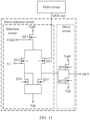
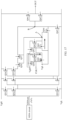
- FIG. 11 is a schematic diagram of a principle of another screen drive circuit according to an embodiment of this application.
- an output terminal of a GOA circuit is connected to an input terminal of a drive selection circuit, a control terminal of the drive selection circuit inputs the row address selection signal CLK2 output by the DDIC, and an output terminal OUT of the drive selection circuit is connected to a row of pixel circuit.
- the drive selection circuit includes a selection circuit and a drive circuit.
- the selection circuit includes switching transistors Q11-Q15, and the drive circuit includes Q16 and Q17 that are connected in series.
- a gate of Q11 inputs the CLK2 signal, a first terminal of Q11 inputs the positive voltage signal VgH, a second terminal of Q11 is connected to a first terminal of Q12, a gate of Q12 inputs the first voltage signal V1, and a second terminal of Q12 is connected to a first terminal of Q14.
- the first terminal of Q12 is further connected to a second terminal of Q13, and a first terminal of Q13 is connected to a first terminal of Q15.
- a gate of Q13 is the input terminal of the drive selection circuit and is connected to the output terminal of the GOA circuit.
- Second terminals of Q14 and Q15 input the negative voltage signal VgL.
- Gates of Q14 and Q15 are both connected to the first terminal of Q14.
- a common terminal of Q13 and Q15 is an output terminal of the selection circuit, and is connected to an input terminal of the drive circuit.
- the input terminal of the drive circuit is gates of Q16 and Q17, a first terminal of Q16 inputs VgH, a second terminal of Q17 inputs VgL, and a drain-source common terminal of Q16 and Q17 is the output terminal OUT of the drive selection circuit.
- the switching transistors Q11, Q12, Q13, and Q16 are all PMOSs, which may be, for example, LTPS-PMOSs.
- the switching transistors Q14, Q15, and Q17 are all NMOSs, which may be, for example, IGZO-NMOSs.
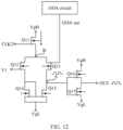
- FIG. 12 is an equivalent circuit diagram of a principle of a drive selection circuit in a case that CLK2 is valid.
- that CLK2 is valid at a low level is used as an example for description.
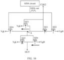
- FIG. 13 is a schematic equivalent circuit diagram of a drive selection circuit in a case that CLK2 is invalid. CLK2 is invalid at a high level.
- the switching transistor Q11 may alternatively be an NMOS.
- CLK2 is valid at a high level and invalid at a low level, and details are not described herein again.
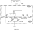
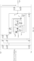
- FIG. 14 is a schematic diagram of a principle of another screen drive circuit according to an embodiment of this application.
- a drive selection circuit includes a selection circuit and a drive circuit.
- the selection circuit includes switching transistors Q21-Q24, and the drive circuit includes switching transistors Q25 and Q26.
- a gate of Q21 inputs the row address selection signal CLK2, Q21 and Q22 are connected in series, a gate of Q22 is connected to an output terminal of a GOA circuit, a first terminal of Q22 inputs the positive voltage signal VgH, a second terminal of Q22 is connected to a first terminal of Q21, and the first terminal of Q21 is connected to an input terminal of the drive circuit.
- a gate of Q24 is connected to the output terminal of the GOA circuit, a first terminal of Q24 is connected to the input terminal of the drive circuit, and a second terminal of Q24 inputs the negative voltage signal VgL.
- the drive circuit includes Q25 and Q26 that are connected in series, gates of Q25 and Q26 are the input terminal of the drive circuit, a first terminal of Q25 is connected to a second terminal of Q26, a second terminal of Q25 inputs VgL, and a first terminal of Q26 inputs VgH.
- a drain-source common terminal of Q25 and Q26 is an output terminal OUT of the drive selection circuit.
- the switching transistors Q23, Q24, and Q25 are all NMOSs, which may be specifically IGZO-NMOSs.
- the switching transistors Q21, Q22, and Q26 are all PMOSs, which may be specifically LTPS-PMOSs.
- Q23 may alternatively be a PMOS transistor, and another switching transistor may correspondingly be a semiconductor transistor of a corresponding type. This application sets no limitation thereto.
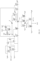
- An output signal GOA out of a GOA circuit is a pulse signal.
- gates of Q31, Q32, and Q33 are connected to an output terminal of a GOA circuit, and sources and drains of Q31, Q32, and Q33 are sequentially connected in series to form a first series branch (that is, a CMOS inverter).
- a first terminal (the drain) of Q31 inputs the positive voltage signal VgH, and the source of Q33 inputs the negative voltage signal VgL.
- Q46 and Q47 may be separately a switching transistor group obtained by connecting a plurality of switching transistors of a same type in parallel, and this application sets no limitation thereto.
- An output terminal GOAout of the GOA circuit outputs a write drive signal (that is, a pulse signal).
- a write drive signal that is, a pulse signal.
- Q33 is on, and Q31 and Q32 are off, to transmit the negative voltage signal VgL to a gate of the second series branch, so that a PMOS transistor in the second series branch is on.
- the positive voltage signal VgH is transmitted to node C, that is, gate voltages of Q34, Q35, and Q45 are VgH, Q34 and Q35 are off, and Q45 is on, so that VgL is transmitted to node B.
- Q46 is on, Q47 is off, and VgH is transmitted to the output terminal OUT by using Q46.
- an output signal of the output terminal OUT is VgH.
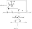
- an embodiment of this application further provides still another screen drive circuit.
- a selection circuit includes switching transistors Q51-Q65, and a drive circuit includes Q66 and Q67.
- the fourth series branch includes two switching transistors Q59 and Q60 that are connected in series over a common gate.
- a second terminal of Q59 is node B, a first terminal of Q60 inputs VgH, and gates of Q59 and Q60 are connected to node A.
- Q59 and Q60 are semiconductor transistors of a same type, and are connected in series over a common gate. Therefore, Q59 and Q60 may be equivalent to one switching transistor, that is, Q56 in FIG. 19 .
- a sixth series branch includes three switching transistors Q63 ⁇ Q65 that are connected in series over a common gate.
- Q64 and Q65 are semiconductor transistors of a same type, which is different from a type of Q63. For example, if Q63 is an NMOS, Q64 and Q65 are PMOSs.
- Q64 and Q65 may be equivalent to one switching transistor. It can be learned that, Q63 ⁇ Q65 form a CMOS inverter.
- Q68 and Q69 are on, so that VgH is transmitted to point D, and further Q57 is on.
- VgL is transmitted to the source of Q58 by using Q57, and a gate voltage of Q58 is VgH. Therefore, Q58 is on, and VgH is transmitted to node B by using Q58.
- Q63 is on, so that VgL is transmitted to node C by using Q63.
- Q67 is on, and finally VgH is transmitted to the output terminal OUT by using Q67. That is, when CLK2 has a low level, GOAout is in a high-level period, and OUT also outputs a high-level signal.
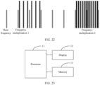
- FIG. 22 is a schematic diagram of a comparison among refresh rates of a base frequency region and frequency multiplication regions.
- a frequency of frequency multiplication 1 is greater than a frequency of a base frequency and is less than a frequency of frequency multiplication 2.
- each partition may be refreshed based on a refresh rate corresponding to its respective partition, and may also be refreshed based on the refresh rate corresponding to the base frequency.
- the disclosed system, apparatus, and method may be implemented in other manners.
- the described apparatus embodiment is merely an example.
- the module or unit division is merely logical function division, and there may be another division manner in actual implementation.
- a plurality of units or components may be combined or integrated into another system, or some features may be ignored or not performed.
- the displayed or discussed mutual couplings or direct couplings or communication connections may be implemented through some interfaces.
- the indirect couplings or communication connections between the apparatuses or units may be implemented in an electrical form, a mechanical form, or another form.
- the units described as separate components may or may not be physically separated, and components displayed as units may or may not be physical units, in other words, may be located in one place, or may be distributed on a plurality of network units. Some or all of the units may be selected based on actual requirements to achieve the objectives of the solutions in embodiments.
- functional units in the embodiments may be integrated into one processing unit, or each of the units may exist alone physically, or two or more units may be integrated into one unit.
- the integrated unit may be implemented in a form of hardware, or may be implemented in a form of a software functional unit.
- the integrated unit When the integrated unit is implemented in the form of the software functional unit and sold or used as an independent product, the integrated unit may be stored in a computer-readable storage medium.
- the computer software product is stored in a storage medium and includes several instructions for instructing a computer device (which may be a personal computer, a server, a network device, or the like) or a processor to perform all or some of the steps of the methods described in the embodiments.
- the foregoing storage medium includes any medium that can store program code, such as a flash memory, a removable hard disk, a read-only memory, a random access memory, a magnetic disk, or an optical disc.
Landscapes
- Engineering & Computer Science (AREA)
- Physics & Mathematics (AREA)
- Computer Hardware Design (AREA)
- General Physics & Mathematics (AREA)
- Theoretical Computer Science (AREA)
- Chemical & Material Sciences (AREA)
- Crystallography & Structural Chemistry (AREA)
- Control Of Indicators Other Than Cathode Ray Tubes (AREA)
Applications Claiming Priority (2)
| Application Number | Priority Date | Filing Date | Title |
|---|---|---|---|
| CN202210482749.9A CN117059033B (zh) | 2022-05-05 | 2022-05-05 | 屏幕驱动电路、显示屏及电子设备 |
| PCT/CN2023/088038 WO2023213175A1 (zh) | 2022-05-05 | 2023-04-13 | 屏幕驱动电路、显示屏及电子设备 |
Publications (2)
| Publication Number | Publication Date |
|---|---|
| EP4398232A1 true EP4398232A1 (de) | 2024-07-10 |
| EP4398232A4 EP4398232A4 (de) | 2025-03-26 |
Family
ID=88646222
Family Applications (1)
| Application Number | Title | Priority Date | Filing Date |
|---|---|---|---|
| EP23799162.5A Pending EP4398232A4 (de) | 2022-05-05 | 2023-04-13 | Bildschirmansteuerungsschaltung, anzeigebildschirm und elektronische vorrichtung |
Country Status (4)
| Country | Link |
|---|---|
| US (1) | US12562127B2 (de) |
| EP (1) | EP4398232A4 (de) |
| CN (1) | CN117059033B (de) |
| WO (1) | WO2023213175A1 (de) |
Cited By (1)
| Publication number | Priority date | Publication date | Assignee | Title |
|---|---|---|---|---|
| EP4468283A4 (de) * | 2022-07-04 | 2025-04-02 | Honor Device Co., Ltd. | Antriebssignalausgabeschaltung, bildschirmantriebsschaltung, anzeigebildschirm und elektronische vorrichtung |
Families Citing this family (9)
| Publication number | Priority date | Publication date | Assignee | Title |
|---|---|---|---|---|
| GB2638079A (en) | 2022-12-19 | 2025-08-13 | Boe Technology Group Co Ltd | Driving circuit, driving method, driving module, and display device |
| CN118891666A (zh) | 2022-12-19 | 2024-11-01 | 京东方科技集团股份有限公司 | 驱动电路、驱动方法、驱动模组和显示装置 |
| US12322343B2 (en) | 2022-12-19 | 2025-06-03 | Chengdu Boe Optoelectronics Technology Co., Ltd. | Driving circuit, driving method, driving module and display device |
| WO2024130491A1 (zh) | 2022-12-19 | 2024-06-27 | 京东方科技集团股份有限公司 | 驱动电路、驱动方法、驱动模组和显示装置 |
| CN118871974B (zh) | 2022-12-19 | 2026-01-02 | 京东方科技集团股份有限公司 | 驱动电路、驱动方法、驱动模组和显示装置 |
| CN119007679B (zh) * | 2024-08-30 | 2025-07-18 | 惠科股份有限公司 | 像素驱动电路、像素驱动方法及显示装置 |
| CN119356782B (zh) * | 2024-10-10 | 2025-09-30 | 武汉凌久微电子有限公司 | 一种基于gpu显示控制器的文本终端刷新方法 |
| CN120472854B (zh) * | 2025-07-11 | 2025-10-03 | 惠科股份有限公司 | 可变刷新率控制电路及其方法、显示面板以及显示设备 |
| CN121393347A (zh) * | 2025-12-25 | 2026-01-23 | 惠科股份有限公司 | 分区刷新电路及其刷新控制方法、显示面板以及显示设备 |
Family Cites Families (17)
| Publication number | Priority date | Publication date | Assignee | Title |
|---|---|---|---|---|
| CN103137081B (zh) * | 2011-11-22 | 2014-12-10 | 上海天马微电子有限公司 | 一种显示面板栅驱动电路及显示屏 |
| CN106663402B (zh) * | 2014-08-05 | 2020-05-19 | 苹果公司 | 使用多个不同刷新速率同时刷新显示设备的多个区域 |
| US9779664B2 (en) * | 2014-08-05 | 2017-10-03 | Apple Inc. | Concurrently refreshing multiple areas of a display device using multiple different refresh rates |
| KR102390093B1 (ko) * | 2015-05-28 | 2022-04-26 | 삼성디스플레이 주식회사 | 게이트 구동 회로 및 표시 장치 |
| KR102458078B1 (ko) * | 2017-08-16 | 2022-10-24 | 엘지디스플레이 주식회사 | 게이트 구동회로와 이를 이용한 표시장치 |
| CN107958655A (zh) * | 2018-01-05 | 2018-04-24 | 京东方科技集团股份有限公司 | 一种液晶显示器和像素单元 |
| CN110910828B (zh) | 2018-09-14 | 2022-01-11 | 华为技术有限公司 | 一种屏幕模组及电子设备 |
| CN111312136B (zh) * | 2018-12-12 | 2022-01-14 | 京东方科技集团股份有限公司 | 移位寄存器单元、扫描驱动电路、驱动方法和显示装置 |
| CN109637478B (zh) * | 2019-01-11 | 2021-01-15 | 昆山龙腾光电股份有限公司 | 一种显示装置及驱动方法 |
| KR102697930B1 (ko) * | 2019-07-29 | 2024-08-26 | 삼성디스플레이 주식회사 | 표시 장치 |
| CN110491331B (zh) * | 2019-09-30 | 2023-01-24 | 京东方科技集团股份有限公司 | 一种显示面板、其驱动方法及显示装置 |
| KR102707322B1 (ko) | 2019-10-11 | 2024-09-20 | 삼성디스플레이 주식회사 | 스캔 드라이버 및 표시 장치 |
| KR102687245B1 (ko) * | 2019-12-18 | 2024-07-22 | 삼성디스플레이 주식회사 | 스캔 드라이버 및 표시 장치 |
| CN210956110U (zh) * | 2019-12-24 | 2020-07-07 | 北京京东方技术开发有限公司 | 一种显示装置 |
| CN112231036A (zh) | 2020-10-21 | 2021-01-15 | 苏州速显微电子科技有限公司 | 一种将显示界面分区域实现不同刷新率刷新的方法 |
| CN113808534B (zh) * | 2021-09-15 | 2023-05-30 | 深圳市华星光电半导体显示技术有限公司 | 显示面板及显示终端 |
| CN113963652B (zh) * | 2021-11-12 | 2023-08-18 | 武汉天马微电子有限公司 | 显示面板及其驱动方法 |
-
2022
- 2022-05-05 CN CN202210482749.9A patent/CN117059033B/zh active Active
-
2023
- 2023-04-13 EP EP23799162.5A patent/EP4398232A4/de active Pending
- 2023-04-13 US US18/703,084 patent/US12562127B2/en active Active
- 2023-04-13 WO PCT/CN2023/088038 patent/WO2023213175A1/zh not_active Ceased
Cited By (1)
| Publication number | Priority date | Publication date | Assignee | Title |
|---|---|---|---|---|
| EP4468283A4 (de) * | 2022-07-04 | 2025-04-02 | Honor Device Co., Ltd. | Antriebssignalausgabeschaltung, bildschirmantriebsschaltung, anzeigebildschirm und elektronische vorrichtung |
Also Published As
| Publication number | Publication date |
|---|---|
| WO2023213175A1 (zh) | 2023-11-09 |
| CN117059033A (zh) | 2023-11-14 |
| US20250246148A1 (en) | 2025-07-31 |
| CN117059033B (zh) | 2024-09-10 |
| EP4398232A4 (de) | 2025-03-26 |
| WO2023213175A9 (zh) | 2024-02-01 |
| US12562127B2 (en) | 2026-02-24 |
Similar Documents
| Publication | Publication Date | Title |
|---|---|---|
| EP4398232A1 (de) | Bildschirmansteuerungsschaltung, anzeigebildschirm und elektronische vorrichtung | |
| US11545093B2 (en) | Shift register, gate driving circuit, display device and gate driving method | |
| KR101475243B1 (ko) | 디스플레이 패널의 게이트 구동 회로 및 이를 갖는 디스플레이 스크린 | |
| US12211413B2 (en) | Gate drive circuit having a shift register unit and control unit and driving method thereof | |
| US11011117B2 (en) | Shift register, drive method thereof, drive control circuit, and display apparatus | |
| US20170178558A1 (en) | Shift register unit and method for driving the same, gate drive circuit and display device | |
| US8134531B2 (en) | Source line driving circuit, active matrix type display device and method for driving the same | |
| GB2550507B (en) | Display panel and driving circuit thereof | |
| US20220284843A1 (en) | Shift register unit, shift register, display panel and driving method thereof | |
| US11232763B2 (en) | Shift register and driving method for compensating for linear pattern appearing on display device | |
| US11183103B2 (en) | Shift register unit and driving method thereof, gate driving circuit, and display device | |
| WO2025247132A1 (zh) | 显示面板、显示装置及驱动方法 | |
| CN118887918A (zh) | 一种显示面板的驱动方法和显示装置 | |
| US12033554B2 (en) | Shift register in display, gate drive circuit, display device, and driving method for same | |
| JP2001325798A (ja) | 論理回路およびこれを用いた表示装置 | |
| EP4468283B1 (de) | Anzeigevorrichtung | |
| CN119785712B (zh) | 一种显示面板和显示装置 | |
| US20250279037A1 (en) | Stage circuit of gate driver and display device including the same | |
| CN120035854B (zh) | 一种移位寄存器、驱动方法、栅极驱动电路及显示装置 | |
| US12236893B2 (en) | Display device using clocks having different frequencies for different display areas | |
| WO2025166648A9 (zh) | 移位寄存器单元及其驱动方法、发光控制电路、显示装置 | |
| WO2024244859A1 (zh) | 栅驱动电路单元及其驱动方法、栅驱动电路和显示装置 | |
| CN120472848A (zh) | 像素驱动电路、显示面板及显示装置 | |
| WO2025166647A1 (zh) | 移位寄存器单元及其驱动方法、栅极驱动电路、显示装置 |
Legal Events
| Date | Code | Title | Description |
|---|---|---|---|
| STAA | Information on the status of an ep patent application or granted ep patent |
Free format text: STATUS: THE INTERNATIONAL PUBLICATION HAS BEEN MADE |
|
| PUAI | Public reference made under article 153(3) epc to a published international application that has entered the european phase |
Free format text: ORIGINAL CODE: 0009012 |
|
| STAA | Information on the status of an ep patent application or granted ep patent |
Free format text: STATUS: REQUEST FOR EXAMINATION WAS MADE |
|
| 17P | Request for examination filed |
Effective date: 20240403 |
|
| AK | Designated contracting states |
Kind code of ref document: A1 Designated state(s): AL AT BE BG CH CY CZ DE DK EE ES FI FR GB GR HR HU IE IS IT LI LT LU LV MC ME MK MT NL NO PL PT RO RS SE SI SK SM TR |
|
| A4 | Supplementary search report drawn up and despatched |
Effective date: 20250224 |
|
| RIC1 | Information provided on ipc code assigned before grant |
Ipc: G09G 3/36 20060101ALI20250219BHEP Ipc: G09G 3/20 20060101AFI20250219BHEP |
|
| DAV | Request for validation of the european patent (deleted) | ||
| DAX | Request for extension of the european patent (deleted) | ||
| STAA | Information on the status of an ep patent application or granted ep patent |
Free format text: STATUS: EXAMINATION IS IN PROGRESS |
|
| 17Q | First examination report despatched |
Effective date: 20250821 |
|
| GRAP | Despatch of communication of intention to grant a patent |
Free format text: ORIGINAL CODE: EPIDOSNIGR1 |
|
| STAA | Information on the status of an ep patent application or granted ep patent |
Free format text: STATUS: GRANT OF PATENT IS INTENDED |
|
| INTG | Intention to grant announced |
Effective date: 20251124 |
|
| GRAS | Grant fee paid |
Free format text: ORIGINAL CODE: EPIDOSNIGR3 |
|
| GRAA | (expected) grant |
Free format text: ORIGINAL CODE: 0009210 |
|
| STAA | Information on the status of an ep patent application or granted ep patent |
Free format text: STATUS: THE PATENT HAS BEEN GRANTED |