EP4395502A2 - Lichtemittierende anzeigevorrichtung - Google Patents
Lichtemittierende anzeigevorrichtung Download PDFInfo
- Publication number
- EP4395502A2 EP4395502A2 EP23212729.0A EP23212729A EP4395502A2 EP 4395502 A2 EP4395502 A2 EP 4395502A2 EP 23212729 A EP23212729 A EP 23212729A EP 4395502 A2 EP4395502 A2 EP 4395502A2
- Authority
- EP
- European Patent Office
- Prior art keywords
- subpixel
- subpixels
- light emitting
- boundary
- trench
- Prior art date
- Legal status (The legal status is an assumption and is not a legal conclusion. Google has not performed a legal analysis and makes no representation as to the accuracy of the status listed.)
- Pending
Links
Images


Classifications
-
- H—ELECTRICITY
- H10—SEMICONDUCTOR DEVICES; ELECTRIC SOLID-STATE DEVICES NOT OTHERWISE PROVIDED FOR
- H10K—ORGANIC ELECTRIC SOLID-STATE DEVICES
- H10K59/00—Integrated devices, or assemblies of multiple devices, comprising at least one organic light-emitting element covered by group H10K50/00
- H10K59/10—OLED displays
- H10K59/12—Active-matrix OLED [AMOLED] displays
- H10K59/121—Active-matrix OLED [AMOLED] displays characterised by the geometry or disposition of pixel elements
- H10K59/1213—Active-matrix OLED [AMOLED] displays characterised by the geometry or disposition of pixel elements the pixel elements being TFTs
-
- H—ELECTRICITY
- H10—SEMICONDUCTOR DEVICES; ELECTRIC SOLID-STATE DEVICES NOT OTHERWISE PROVIDED FOR
- H10K—ORGANIC ELECTRIC SOLID-STATE DEVICES
- H10K50/00—Organic light-emitting devices
- H10K50/80—Constructional details
- H10K50/805—Electrodes
- H10K50/81—Anodes
-
- H—ELECTRICITY
- H10—SEMICONDUCTOR DEVICES; ELECTRIC SOLID-STATE DEVICES NOT OTHERWISE PROVIDED FOR
- H10K—ORGANIC ELECTRIC SOLID-STATE DEVICES
- H10K50/00—Organic light-emitting devices
- H10K50/80—Constructional details
- H10K50/805—Electrodes
- H10K50/82—Cathodes
-
- H—ELECTRICITY
- H10—SEMICONDUCTOR DEVICES; ELECTRIC SOLID-STATE DEVICES NOT OTHERWISE PROVIDED FOR
- H10K—ORGANIC ELECTRIC SOLID-STATE DEVICES
- H10K50/00—Organic light-emitting devices
- H10K50/80—Constructional details
- H10K50/85—Arrangements for extracting light from the devices
- H10K50/856—Arrangements for extracting light from the devices comprising reflective means
-
- H—ELECTRICITY
- H10—SEMICONDUCTOR DEVICES; ELECTRIC SOLID-STATE DEVICES NOT OTHERWISE PROVIDED FOR
- H10K—ORGANIC ELECTRIC SOLID-STATE DEVICES
- H10K59/00—Integrated devices, or assemblies of multiple devices, comprising at least one organic light-emitting element covered by group H10K50/00
- H10K59/10—OLED displays
- H10K59/12—Active-matrix OLED [AMOLED] displays
- H10K59/121—Active-matrix OLED [AMOLED] displays characterised by the geometry or disposition of pixel elements
-
- H—ELECTRICITY
- H10—SEMICONDUCTOR DEVICES; ELECTRIC SOLID-STATE DEVICES NOT OTHERWISE PROVIDED FOR
- H10K—ORGANIC ELECTRIC SOLID-STATE DEVICES
- H10K59/00—Integrated devices, or assemblies of multiple devices, comprising at least one organic light-emitting element covered by group H10K50/00
- H10K59/10—OLED displays
- H10K59/12—Active-matrix OLED [AMOLED] displays
- H10K59/122—Pixel-defining structures or layers, e.g. banks
-
- H—ELECTRICITY
- H10—SEMICONDUCTOR DEVICES; ELECTRIC SOLID-STATE DEVICES NOT OTHERWISE PROVIDED FOR
- H10K—ORGANIC ELECTRIC SOLID-STATE DEVICES
- H10K59/00—Integrated devices, or assemblies of multiple devices, comprising at least one organic light-emitting element covered by group H10K50/00
- H10K59/10—OLED displays
- H10K59/12—Active-matrix OLED [AMOLED] displays
- H10K59/123—Connection of the pixel electrodes to the thin film transistors [TFT]
-
- H—ELECTRICITY
- H10—SEMICONDUCTOR DEVICES; ELECTRIC SOLID-STATE DEVICES NOT OTHERWISE PROVIDED FOR
- H10K—ORGANIC ELECTRIC SOLID-STATE DEVICES
- H10K59/00—Integrated devices, or assemblies of multiple devices, comprising at least one organic light-emitting element covered by group H10K50/00
- H10K59/10—OLED displays
- H10K59/12—Active-matrix OLED [AMOLED] displays
- H10K59/124—Insulating layers formed between TFT elements and OLED elements
-
- H—ELECTRICITY
- H10—SEMICONDUCTOR DEVICES; ELECTRIC SOLID-STATE DEVICES NOT OTHERWISE PROVIDED FOR
- H10K—ORGANIC ELECTRIC SOLID-STATE DEVICES
- H10K59/00—Integrated devices, or assemblies of multiple devices, comprising at least one organic light-emitting element covered by group H10K50/00
- H10K59/30—Devices specially adapted for multicolour light emission
- H10K59/35—Devices specially adapted for multicolour light emission comprising red-green-blue [RGB] subpixels
-
- H—ELECTRICITY
- H10—SEMICONDUCTOR DEVICES; ELECTRIC SOLID-STATE DEVICES NOT OTHERWISE PROVIDED FOR
- H10K—ORGANIC ELECTRIC SOLID-STATE DEVICES
- H10K59/00—Integrated devices, or assemblies of multiple devices, comprising at least one organic light-emitting element covered by group H10K50/00
- H10K59/30—Devices specially adapted for multicolour light emission
- H10K59/35—Devices specially adapted for multicolour light emission comprising red-green-blue [RGB] subpixels
- H10K59/351—Devices specially adapted for multicolour light emission comprising red-green-blue [RGB] subpixels comprising more than three subpixels, e.g. red-green-blue-white [RGBW]
-
- H—ELECTRICITY
- H10—SEMICONDUCTOR DEVICES; ELECTRIC SOLID-STATE DEVICES NOT OTHERWISE PROVIDED FOR
- H10K—ORGANIC ELECTRIC SOLID-STATE DEVICES
- H10K59/00—Integrated devices, or assemblies of multiple devices, comprising at least one organic light-emitting element covered by group H10K50/00
- H10K59/30—Devices specially adapted for multicolour light emission
- H10K59/35—Devices specially adapted for multicolour light emission comprising red-green-blue [RGB] subpixels
- H10K59/353—Devices specially adapted for multicolour light emission comprising red-green-blue [RGB] subpixels characterised by the geometrical arrangement of the RGB subpixels
-
- H—ELECTRICITY
- H10—SEMICONDUCTOR DEVICES; ELECTRIC SOLID-STATE DEVICES NOT OTHERWISE PROVIDED FOR
- H10K—ORGANIC ELECTRIC SOLID-STATE DEVICES
- H10K59/00—Integrated devices, or assemblies of multiple devices, comprising at least one organic light-emitting element covered by group H10K50/00
- H10K59/80—Constructional details
- H10K59/805—Electrodes
- H10K59/8051—Anodes
- H10K59/80515—Anodes characterised by their shape
-
- H—ELECTRICITY
- H10—SEMICONDUCTOR DEVICES; ELECTRIC SOLID-STATE DEVICES NOT OTHERWISE PROVIDED FOR
- H10K—ORGANIC ELECTRIC SOLID-STATE DEVICES
- H10K59/00—Integrated devices, or assemblies of multiple devices, comprising at least one organic light-emitting element covered by group H10K50/00
- H10K59/80—Constructional details
- H10K59/875—Arrangements for extracting light from the devices
- H10K59/876—Arrangements for extracting light from the devices comprising a resonant cavity structure, e.g. Bragg reflector pair
Definitions
- the present invention relates to a light emitting display device.
- a light emitting display device uses a light emitting element in which charges are injected into a light emitting layer formed between a cathode as an electron injection electrode and an anode as a hole injection electrode so that electrons and holes pair up and then annihilate to emit light.
- the light emitting layer is formed on the entire surface of the substrate through a deposition process without a separate mask.
- adjacent subpixels are electrically connected through the light emitting layer, allowing leakage current to flow to the adjacent subpixels.
- the possibility of occurrence of such the leakage current increases as display devices become higher resolution.
- image quality of the display device deteriorates.
- the present invention is directed to a light emitting display device that substantially obviates one or more of the problems due to limitations and disadvantages of the related art.
- An advantage of the present invention is to provide a light emitting display device which can prevent leakage current between adjacent subpixels.
- a light emitting display device includes: a substrate on which a plurality of subpixels arranged in a matrix form along a plurality of row lines and a plurality of column lines are defined; a first electrode formed for each subpixel on the substrate; a bank that which covers an edge of the first electrode and includes a trench formed along a boundary between neighboring subpixels; a light emitting layer located on the first electrode and separated for each subpixel by the trench; and a second electrode formed on the light emitting layers of the plurality of subpixels, wherein the subpixel has a quadrangular protruding corner portion and three inclined corners portions, wherein the plurality of subpixels include first and second subpixels adjacent to each other in a row direction, and fourth and third subpixels that are respectively adjacent to the first and second subpixels in a column direction, wherein the trench includes: a first corner groove in a second diagonal direction which is formed at
- a light emitting display device includes: a substrate on which a plurality of subpixels arranged in a matrix form along a plurality of row lines and a plurality of column lines are defined; a first electrode formed for each subpixel on the substrate; a bank that which covers an edge of the first electrode and includes a trench formed along a boundary between neighboring subpixels; a light emitting layer located on the first electrode and separated for each subpixel by the trench; and a second electrode formed on the light emitting layers of the plurality of subpixels, wherein the trench includes: a first trench line along a boundary between neighboring column lines; and a second trench line along a boundary between neighboring row lines, wherein the first trench line includes a first side groove in a column direction, and first and second corner grooves that are connected between adjacent first side grooves, form an isosceles portion protruding to one side in a row direction, have second and first diagonal directions, respectively, and are connected to each other at a first contact point, wherein the second
- FIG. 1 is a plan view schematically illustrating a light emitting display device according to a first embodiment of the present invention.
- FIG. 2 is a cross-sectional view taken along a line II-II' of FIG. 1 and schematically shows a cross-sectional structure of subpixels.
- the plurality of subpixels SP may include subpixels that constitute a unit pixel and display first, second and third colors as different colors, for example, red (R), green (G), and blue (B) subpixels respectively displaying red, green, and blue.
- the plurality of subpixels SP may further include a subpixel displaying white.
- the plurality of thin film transistors TR may be formed in each subpixel SP on the substrate 101. Meanwhile, in this embodiment, for convenience of explanation, one thin film transistor TR connected to the light emitting diode OD in the subpixel SP is shown. Meanwhile, the thin film transistor TR in FIG. 2 may be a driving thin film transistor, but is not limited thereto.
- the first insulating layer 111 may be formed substantially on the entire surface of the substrate 101 while covering the thin film transistor TR.
- the first insulating layer 111 may be made of an organic insulating material or an inorganic insulating material.
- a first reflector 121 may be formed within the R subpixel SP.
- the second insulating layer 112 may be formed the first insulating layer 111 on which the first reflector 121 is formed and substantially over the entire surface of the substrate 101.
- the second insulating layer 112 may be made of an organic insulating material or an inorganic insulating material.
- a second reflector 122 may be formed within the G subpixel SP.
- the third insulating layer 113 may be formed on the second insulating layer 112 on which the second reflector 122 is formed and substantially over the entire surface of the substrate 101.
- the third insulating layer 113 may be made of an organic insulating material or an inorganic insulating material.
- a contact hole CH exposing one electrode, for example, a drain electrode, of the thin film transistor TR may be formed in the first to third insulating layers 111 to 113.
- the light emitting layer 145 may be separated (or disconnected or divided) in a unit of each subpixel SP by the trench TC surrounding each subpixel SP and be formed in a pattern corresponding to each subpixel SP.
- the light emitting layer 145 may have a single-layer stack structure or a multi-layer stack structure. When the light emitting layer 145 has a single-layer stack structure, it may be completely separated into subpixels SP by the trench TC.
- the trench TC may be formed along the boundary of the subpixel SP, so that the light emitting layers 145 between the neighboring subpixels SP may be physically separated from each other. Accordingly, occurrence of leakage current through the light emitting layer 145 between the neighboring subpixels SP can be prevented.
- the second electrode 150 may be formed of a metal material having a transflective property, for example, magnesium (Mg), silver (Ag), or an alloy of magnesium (Mg) and silver (Ag).
- a metal material having a transflective property for example, magnesium (Mg), silver (Ag), or an alloy of magnesium (Mg) and silver (Ag).
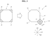
- the second, third, and fourth corner portions C2, C3, and C4, which are the remaining inclined corner portions of each subpixel SP, may be arranged, for example, in a clockwise direction.
- the second, third, and fourth corner portions C2, C3, and C4 may be respectively located on the lower left side of the second diagonal direction DD2, the upper left side of the first diagonal direction DD1, and the upper right side of the second diagonal direction DD2.
- the second and fourth subpixels SP2 and SP4 adjacent in the second diagonal direction DD2 may be spaced apart from each other with the first corner portion C1 of the first subpixel SP1 interposed therebetween.
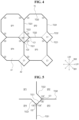
- the subpixel SP located in the odd column line may have its protruding corner portion located on the lower right side and facing the first diagonal direction DD1
- the subpixel SP located in the even column line may have its protruding corner located on the upper right side and facing the second diagonal direction DD2.
- the first trench line and the second trench line may alternately share the first and second corner grooves TCC1 and TCC2 of the protruding corner portion Cp.
- the subpixel SP may have four corner portions, of which three corner portions may have an inclined chamfer shape and the remaining corner portion Cp may have a protruding square shape.
- the first region A1 may have three corner portions in a chamfer shape, and the second region A2 may have one corner portion Cp in a protruding form.
- a light emitting diode may be provided at the emission region in the first region A1.
- the light emitting diode and a thin film transistor may be connected to each other.
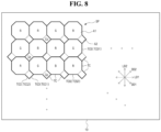
- a trench TC surrounding each subpixel SP may be formed along a boundary of each subpixel SP. As such, the trench TC may be formed at the boundary between the neighboring subpixels SP to separate them.
- the protruding corner portions Cp may be configured to alternate in direction along the column line.
- the subpixels SP arranged along each column line may be configured such that the directions of the protruding corner portions Cp may alternate in the first diagonal direction DD1 and the second diagonal direction DD2.
- the subpixel SP located in the odd row line may have its protruding corner portion located on the lower right side and facing the first diagonal direction DD1
- the subpixel SP located in the even row line may have its protruding corner located on the lower left side and facing the second diagonal direction DD2.
- a first trench line which is the trench TC disposed in the boundary line that is located on one side, for example, on the right side of the subpixels SP on each column line and extends along the column line (or a boundary line which is between the neighboring column lines), may have a shape that alternately protrudes to the right and left along the shape of the protruding corner portion Cp.
- the first trench line may be configured with the first side grooves TCS1 in the column direction LD2, and the first and second corner grooves TCC1 and TCC2 which are connected between the neighboring first side grooves TCS1 and form a part protruding in a form of a right-angled isosceles.
- a second trench line which is the trench TC disposed in the boundary line that is located on one side, for example, on the lower side of the subpixels SP on each row line and extends along the row line (or a boundary line which is between the neighboring row lines), may have a shape that protrudes downward along the shape of the protruding corner portion Cp.
- the first trench line and the second trench line may alternately share the first and second corner grooves TCC1 and TCC2 of the protruding corner portion Cp.
- the subpixels SP surrounded by them may be defined.
- the protruding corner portions Cp may be alternately arranged in opposite diagonal directions on the column line. In this way, subpixel patterns in the same direction are not repeated, and phenomenon of the same pattern being visible can be relieved.
- the light emitting display device 10 of this embodiment can have the effects and advantages mentioned in the first embodiment.
- the trench is formed along the boundary of the subpixel, so that the light emitting layers of the neighboring subpixels can be physically separated from each other. Accordingly, the occurrence of leakage current through the light emitting layer between the neighboring subpixels can be prevented.
- the trench which is formed at the boundaries between the adjacent subpixels meeting each other, can be formed in a "Y" shape with intersection angles of 90 degrees, 135 degrees, and 135 degrees, the trench of the desired width can be formed through a mask process using the OPC design. As a result, the light emitting layer can be separated between the neighboring subpixels by the trench.
- protruding corner portions can be alternately arranged in opposite diagonal directions on the row line or column line. In this case, subpixel patterns in the same direction are not repeated, and the phenomenon of the same pattern being visible can be relieved.
Landscapes
- Engineering & Computer Science (AREA)
- Microelectronics & Electronic Packaging (AREA)
- Physics & Mathematics (AREA)
- Optics & Photonics (AREA)
- Geometry (AREA)
- Electroluminescent Light Sources (AREA)
- Devices For Indicating Variable Information By Combining Individual Elements (AREA)
Applications Claiming Priority (1)
| Application Number | Priority Date | Filing Date | Title |
|---|---|---|---|
| KR1020220188261A KR20240105832A (ko) | 2022-12-29 | 2022-12-29 | 발광표시장치 |
Publications (2)
| Publication Number | Publication Date |
|---|---|
| EP4395502A2 true EP4395502A2 (de) | 2024-07-03 |
| EP4395502A3 EP4395502A3 (de) | 2024-10-23 |
Family
ID=88978513
Family Applications (1)
| Application Number | Title | Priority Date | Filing Date |
|---|---|---|---|
| EP23212729.0A Pending EP4395502A3 (de) | 2022-12-29 | 2023-11-28 | Lichtemittierende anzeigevorrichtung |
Country Status (6)
| Country | Link |
|---|---|
| US (1) | US20240224688A1 (de) |
| EP (1) | EP4395502A3 (de) |
| JP (2) | JP2024096016A (de) |
| KR (1) | KR20240105832A (de) |
| CN (1) | CN118284154A (de) |
| TW (1) | TWI872834B (de) |
Families Citing this family (1)
| Publication number | Priority date | Publication date | Assignee | Title |
|---|---|---|---|---|
| TW202226641A (zh) * | 2020-11-26 | 2022-07-01 | 日商索尼集團公司 | 顯示裝置、電子機器及顯示裝置之製造方法 |
Family Cites Families (14)
| Publication number | Priority date | Publication date | Assignee | Title |
|---|---|---|---|---|
| KR100741967B1 (ko) * | 2004-11-08 | 2007-07-23 | 삼성에스디아이 주식회사 | 평판표시장치 |
| JP2016057488A (ja) * | 2014-09-10 | 2016-04-21 | 株式会社ジャパンディスプレイ | 自発光型表示装置 |
| KR102433274B1 (ko) * | 2017-11-28 | 2022-08-18 | 삼성디스플레이 주식회사 | 유기 발광 표시 장치 |
| KR102514205B1 (ko) * | 2017-12-07 | 2023-03-27 | 엘지디스플레이 주식회사 | 유기발광 표시장치 |
| US11088339B2 (en) * | 2018-07-31 | 2021-08-10 | Lg Display Co., Ltd. | Electroluminescent display device |
| KR102646218B1 (ko) * | 2018-11-02 | 2024-03-08 | 엘지디스플레이 주식회사 | 전계 발광 표시 장치 |
| KR102844770B1 (ko) * | 2018-12-13 | 2025-08-08 | 엘지디스플레이 주식회사 | 전계발광 표시장치 및 그를 포함한 개인 몰입형 표시장치 |
| JP2019117941A (ja) * | 2019-03-19 | 2019-07-18 | セイコーエプソン株式会社 | 電気光学装置 |
| KR20210114094A (ko) * | 2020-03-09 | 2021-09-23 | 삼성디스플레이 주식회사 | 디스플레이 장치 |
| CN111710792B (zh) * | 2020-06-30 | 2023-05-02 | 云谷(固安)科技有限公司 | 显示面板及显示面板的制备方法 |
| KR20220020166A (ko) * | 2020-08-11 | 2022-02-18 | 엘지디스플레이 주식회사 | 표시 장치 |
| KR20220035646A (ko) * | 2020-09-14 | 2022-03-22 | 엘지디스플레이 주식회사 | 표시 장치 |
| KR102933781B1 (ko) * | 2020-09-16 | 2026-03-03 | 엘지디스플레이 주식회사 | 표시장치 |
| JP7657597B2 (ja) * | 2021-01-21 | 2025-04-07 | 株式会社ジャパンディスプレイ | 表示装置 |
-
2022
- 2022-12-29 KR KR1020220188261A patent/KR20240105832A/ko active Pending
-
2023
- 2023-11-28 EP EP23212729.0A patent/EP4395502A3/de active Pending
- 2023-11-28 US US18/521,844 patent/US20240224688A1/en active Pending
- 2023-11-29 TW TW112146425A patent/TWI872834B/zh active
- 2023-12-15 JP JP2023211867A patent/JP2024096016A/ja active Pending
- 2023-12-28 CN CN202311830904.2A patent/CN118284154A/zh active Pending
-
2025
- 2025-10-24 JP JP2025179358A patent/JP2026010189A/ja active Pending
Also Published As
| Publication number | Publication date |
|---|---|
| EP4395502A3 (de) | 2024-10-23 |
| JP2026010189A (ja) | 2026-01-21 |
| KR20240105832A (ko) | 2024-07-08 |
| TW202442097A (zh) | 2024-10-16 |
| CN118284154A (zh) | 2024-07-02 |
| JP2024096016A (ja) | 2024-07-11 |
| TWI872834B (zh) | 2025-02-11 |
| US20240224688A1 (en) | 2024-07-04 |
Similar Documents
| Publication | Publication Date | Title |
|---|---|---|
| US11871634B2 (en) | Display device | |
| CN112534583B (zh) | 显示基板、显示装置及高精度金属掩模板 | |
| US9305489B2 (en) | Organic light emitting diode display | |
| CN114450802B (zh) | 一种显示面板、掩膜组件和显示装置 | |
| JP7621981B2 (ja) | 表示装置、表示パネル及びその製造方法 | |
| US11587986B2 (en) | Organic light emitting display device including reflection structure | |
| CN116075188B (zh) | 一种显示基板及显示装置 | |
| JP7561816B2 (ja) | ディスプレイ装置 | |
| JP2023145605A (ja) | 表示装置、および電子機器 | |
| JP2026010189A (ja) | 発光表示装置 | |
| CN115148759A (zh) | 显示基板及显示装置 | |
| US12520666B2 (en) | Display substrate and display device | |
| KR20230173983A (ko) | 디스플레이 장치 | |
| KR102778154B1 (ko) | 표시 장치 | |
| US20250098469A1 (en) | Light emitting display device | |
| WO2023039792A1 (zh) | 显示面板和显示装置 | |
| JP2025070987A (ja) | 表示パネル | |
| JP2025105460A (ja) | ディスプレイパネルおよびディスプレイ装置 | |
| KR20260026955A (ko) | 디스플레이 장치 | |
| JP2025517679A (ja) | 有機発光表示装置 | |
| CN118120349A (zh) | 显示面板和显示装置 | |
| WO2026044716A1 (zh) | 显示面板及显示装置 | |
| CN116367603A (zh) | 显示装置 | |
| CN116264803A (zh) | 显示装置 | |
| KR20220096852A (ko) | 표시 장치 |
Legal Events
| Date | Code | Title | Description |
|---|---|---|---|
| PUAI | Public reference made under article 153(3) epc to a published international application that has entered the european phase |
Free format text: ORIGINAL CODE: 0009012 |
|
| STAA | Information on the status of an ep patent application or granted ep patent |
Free format text: STATUS: REQUEST FOR EXAMINATION WAS MADE |
|
| 17P | Request for examination filed |
Effective date: 20231128 |
|
| AK | Designated contracting states |
Kind code of ref document: A2 Designated state(s): AL AT BE BG CH CY CZ DE DK EE ES FI FR GB GR HR HU IE IS IT LI LT LU LV MC ME MK MT NL NO PL PT RO RS SE SI SK SM TR |
|
| PUAL | Search report despatched |
Free format text: ORIGINAL CODE: 0009013 |
|
| AK | Designated contracting states |
Kind code of ref document: A3 Designated state(s): AL AT BE BG CH CY CZ DE DK EE ES FI FR GB GR HR HU IE IS IT LI LT LU LV MC ME MK MT NL NO PL PT RO RS SE SI SK SM TR |
|
| RIC1 | Information provided on ipc code assigned before grant |
Ipc: H10K 59/80 20230101ALI20240917BHEP Ipc: H10K 59/122 20230101ALI20240917BHEP Ipc: H10K 59/121 20230101AFI20240917BHEP |
|
| RIC1 | Information provided on ipc code assigned before grant |
Ipc: H10K 59/121 20230101AFI20250815BHEP Ipc: H10K 59/122 20230101ALI20250815BHEP Ipc: H10K 59/80 20230101ALI20250815BHEP |
|
| GRAP | Despatch of communication of intention to grant a patent |
Free format text: ORIGINAL CODE: EPIDOSNIGR1 |
|
| STAA | Information on the status of an ep patent application or granted ep patent |
Free format text: STATUS: GRANT OF PATENT IS INTENDED |
|
| INTG | Intention to grant announced |
Effective date: 20251007 |
|
| GRAJ | Information related to disapproval of communication of intention to grant by the applicant or resumption of examination proceedings by the epo deleted |
Free format text: ORIGINAL CODE: EPIDOSDIGR1 |
|
| STAA | Information on the status of an ep patent application or granted ep patent |
Free format text: STATUS: REQUEST FOR EXAMINATION WAS MADE |
|
| GRAP | Despatch of communication of intention to grant a patent |
Free format text: ORIGINAL CODE: EPIDOSNIGR1 |
|
| STAA | Information on the status of an ep patent application or granted ep patent |
Free format text: STATUS: GRANT OF PATENT IS INTENDED |
|
| INTC | Intention to grant announced (deleted) | ||
| INTG | Intention to grant announced |
Effective date: 20260309 |