EP4386830A1 - Sicherungsstruktur mit metallischem heizer und wärmeverteilungsstruktur für sicherungskörper - Google Patents
Sicherungsstruktur mit metallischem heizer und wärmeverteilungsstruktur für sicherungskörper Download PDFInfo
- Publication number
- EP4386830A1 EP4386830A1 EP23201726.9A EP23201726A EP4386830A1 EP 4386830 A1 EP4386830 A1 EP 4386830A1 EP 23201726 A EP23201726 A EP 23201726A EP 4386830 A1 EP4386830 A1 EP 4386830A1
- Authority
- EP
- European Patent Office
- Prior art keywords
- fuse
- metal
- heater
- fuse body
- metal heater
- Prior art date
- Legal status (The legal status is an assumption and is not a legal conclusion. Google has not performed a legal analysis and makes no representation as to the accuracy of the status listed.)
- Pending
Links
Images









Classifications
-
- H—ELECTRICITY
- H10—SEMICONDUCTOR DEVICES; ELECTRIC SOLID-STATE DEVICES NOT OTHERWISE PROVIDED FOR
- H10W—GENERIC PACKAGES, INTERCONNECTIONS, CONNECTORS OR OTHER CONSTRUCTIONAL DETAILS OF DEVICES COVERED BY CLASS H10
- H10W20/00—Interconnections in chips, wafers or substrates
- H10W20/40—Interconnections external to wafers or substrates, e.g. back-end-of-line [BEOL] metallisations or vias connecting to gate electrodes
- H10W20/49—Adaptable interconnections, e.g. fuses or antifuses
- H10W20/493—Fuses, i.e. interconnections changeable from conductive to non-conductive
-
- H—ELECTRICITY
- H10—SEMICONDUCTOR DEVICES; ELECTRIC SOLID-STATE DEVICES NOT OTHERWISE PROVIDED FOR
- H10W—GENERIC PACKAGES, INTERCONNECTIONS, CONNECTORS OR OTHER CONSTRUCTIONAL DETAILS OF DEVICES COVERED BY CLASS H10
- H10W20/00—Interconnections in chips, wafers or substrates
- H10W20/40—Interconnections external to wafers or substrates, e.g. back-end-of-line [BEOL] metallisations or vias connecting to gate electrodes
- H10W20/41—Interconnections external to wafers or substrates, e.g. back-end-of-line [BEOL] metallisations or vias connecting to gate electrodes characterised by their conductive parts
- H10W20/44—Conductive materials thereof
- H10W20/4451—Semiconductor materials, e.g. polysilicon
-
- H—ELECTRICITY
- H10—SEMICONDUCTOR DEVICES; ELECTRIC SOLID-STATE DEVICES NOT OTHERWISE PROVIDED FOR
- H10W—GENERIC PACKAGES, INTERCONNECTIONS, CONNECTORS OR OTHER CONSTRUCTIONAL DETAILS OF DEVICES COVERED BY CLASS H10
- H10W40/00—Arrangements for thermal protection or thermal control
- H10W40/10—Arrangements for heating
Definitions
- the present disclosure relates to fuses, and more specifically, to a fuse structure including a polysilicon fuse body with a metal heater and a heat spreading structure.
- E-fuses can be 'programmed' to change interconnections within the IC. More particularly, a fuse body or link can be caused to stop or greatly reduce current flow therethrough by application of a prescribed current controlled, for example, by a transistor. Once sufficient changes have occurred in the fuse body, the fuse body is open or blown, stopping or greatly reducing current from passing through the fuse.
- One common fuse includes a fuse body made of polysilicon.
- polysilicon e-fuses can be heated to reduce the amount of current required to program them. However, current heating approaches are ineffective at delivering sufficient heat to reduce the current required to program the fuse.
- An aspect of the disclosure provides a fuse structure, comprising: a fuse body including a polysilicon; a metal heater over the fuse body; and a heating spreading structure thermally coupled to the metal heater and extending horizontally adjacent to at least one side of the fuse body.
- An aspect of the disclosure provides a fuse structure comprising: a fuse body on a dielectric layer, the fuse body including a polysilicon; a first fuse electrode and a second fuse electrode coupled to respective opposite ends of the fuse body; a metal heater above the fuse body and laterally overlapping at least a portion of the fuse body; a first heater electrode and a fourth heater electrode coupled to respective opposite ends of the metal heater and defining an electrical current path through the metal heater; and a heat spreading structure extending adjacent to the fuse body, the heat spreading structure coupled to the metal heater.
- An aspect of the disclosure provides a method for heating a fuse in an integrated circuit (IC) structure, the fuse including a fuse body including polysilicon, the method comprising: heating an area over the fuse body using a metal heater; and spreading heat from the metal heater through a heat spreading structure thermally coupled to the metal heater and extending horizontally adjacent to at least one side of the fuse body.
- IC integrated circuit
- such phrasing is intended to encompass the first listed option (A) only, or the selection of the second listed option (B) only, or the selection of the third listed option (C) only, or the selection of the first and the second listed options (A and B), or the selection of the first and third listed options (A and C) only, or the selection of the second and third listed options (B and C) only, or the selection of all three options (A and B and C).
- This may be extended, as readily apparent by one of ordinary skill in the art, for as many items listed.
- Embodiments of the disclosure include a fuse structure having a fuse body including a polysilicon, and a metal heater over the fuse body.
- the fuse structure also includes a heat spreading structure thermally coupled to the metal heater and extending horizontally adjacent to at least one side of the fuse body.
- the metal heater can be a portion of a metal wire or a resistor including a resistive metal.
- the heat spreading structure may include a plurality of metal contacts.
- the fuse structure including the heat spreading structure reduces the necessary programming energy and also reduces the size of a programming current source, which will reduce the overall circuitry footprint.
- the fuse structure does not require any additional masks to implement.
- FIG. 1 shows a perspective view of a fuse structure 100 according to embodiments of the disclosure.
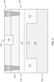
- FIG. 2 shows a Y cross-sectional view of fuse structure 100 in FIG. 1 along view line 2-2 (across fuse body 102), and
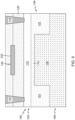
- FIG. 3 shows an X cross-sectional view of fuse structure 100 in FIG. 1 along view line 3-3 (through fuse body 102).
- Fuse structure 100 includes a fuse body 102 including a polysilicon.
- the polysilicon can be any polysilicon used for fuses and/or during formation of other devices such as transistor or resistors (not shown) over an active region 106 of an integrated circuit (IC) structure 104. That is, fuse body 102 may be formed as part of active region 106 of a substrate 108 in IC structure 104 in which fuse structure 100 is used.
- substrate 108 is shown as a bulk semiconductor substrate, but it may include any now known or later developed substrate, e.g., fin, nanosheets, semiconductor-on-insulator (SOI).
- Fuse body 102 may include a polysilicon body 110.
- Polysilicon body 110 may have a pair of spacers 112 ( FIG.
- Spacers 112 may include any now known or later developed spacer material such as but not limited to silicon nitride. Spacers 112 may be omitted in some cases.
- Fuse body 102 is on a dielectric layer 114.
- Dielectric layer 114 may include any now known or later developed gate dielectric materials such as but not limited to hafnium silicate (HfSiO), hafnium oxide (HfO 2 ), zirconium silicate (ZrSiO x ), zirconium oxide(ZrO 2 ), silicon oxide (SiO 2 ), silicon nitride (Si 3 N 4 ), silicon oxynitride (SiON), high-k material or any combination of these materials.
- fuse structure 100 may include a first fuse electrode 116 and a second fuse electrode 118 coupled to respective opposite ends of fuse body 102.
- Fuse electrodes 116, 118 may include any form of metal contacts and/or wires extending through interlayer dielectric (ILD) layer(s) 120 ( FIG. 3 ) above fuse body 102.
- ILD interlayer dielectric
- Active region 106 and fuse structure 100 may be further electrically isolated by any variety of trench isolations 122, e.g., trenches filled with silicon oxide.
- Fuse structure 100 also includes a metal heater 130 over fuse body 102. As shown in FIG. 1 , metal heater 130 (laterally) overlaps at least a portion of fuse body 102 such that heat produced by metal heater 130 heats fuse body 102. A dielectric layer (portion of ILD layer(s) 120) is between fuse body 102 and particularly, polysilicon body 110 thereof and metal heater 130. As will be described, metal heater 130 can take a variety of forms according to embodiments of the disclosure.
- metal heater 130 includes at least a portion of a metal wire 132.
- Metal wire 132 can be any now known or later developed wire structure found in IC structure 104.
- Metal wire 132 and any metal contacts (described herein) can be formed using any now known or later developed semiconductor fabrication techniques. In one non-limiting example, metal wires and metal contacts may be formed by patterning a mask, etching wire and/or contact openings in respective dielectric layer(s). The metal may include refractory metal liner and a metal body.
- the refractory metal liner may include, for example, ruthenium (Ru), tantalum (Ta), titanium (Ti), tungsten (W), iridium (Ir), rhodium (Rh) and platinum (Pt), etc., or mixtures of thereof.
- the metal body may be any now known or later developed contact or wire metal such as but not limited to copper (Cu) or tungsten (W).
- Metal wires 132 may run laterally in any manner required to route electrical signals.
- Metal heater 130 may also include a first heater electrode 134 and a second heater electrode 136 coupled to respective opposite ends of metal heater 130 and defining an electrical current path through metal wire 132 of metal heater 130.
- electrodes 134, 136 are shown (dashed lines) as portions of metal wire 132, but could also include metal contacts to the opposite ends of metal heater 130.
- Fuse structure 100 also includes a heating spreading structure 140 thermally coupled to metal heater 130 and extending horizontally adjacent to at least one side of fuse body 102.
- heat spreading structure 140 includes a plurality of metal contacts 142.
- Metal contacts 142 in IC structure 104 can take a couple of forms. Certain metal contacts, such as those used as electrodes 116, 118 for fuse body 102, are operative metal contacts and carry electrical signals/current.
- Metal contacts 142 that are part of heat spreading structure 140 have the same physical structure as operative metal contacts, but in certain embodiments, may be used solely for communication of heat (thermal communication) from metal heater 130 to fuse body 102 and do not necessarily carry an electrical signal/current.
- operative metal contacts such as electrodes 116, 118 may run vertically in any manner required to route electrical signals.
- metal contacts 142 of heat spreading structure 140 may run vertically in any manner to mainly direct heat to fuse body 102. As will be described, in some cases metal contacts 142 may transmit heat and carry current.
- heat spreading structure 140 e.g., metal contacts 142
- metal contacts 142 extend vertically to be horizontally adjacent to pair of spacers 112 of fuse body 102.
- Metal contacts 142 do not land on fuse body 102, and may partially land on spacers 112 or land on active region 106 adjacent to fuse body 102.
- metal contacts 142 of heat spreading structure 140 are outside the electrical current path of metal heater 130, i.e., there is no current running through metal contacts 142 in this embodiment. Heat from metal heater 130 is delivered by heat spreading structure 140 closer to fuse body 102 than in conventional fuse structures, reducing the necessary programming energy necessary for fuse structure 100.
- Fuse structure 100 with heat spreading structure 140 also reduces the size of a required programming current source, which reduces the overall circuitry footprint. Also, advantageously, fuse structure 100 does not require any additional masks to implement - metal contacts 142 can be formed at the same time as other operative metal contacts (e.g., electrodes 116, 118 of fuse body 102) of IC structure 104.
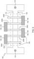
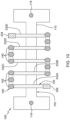
- Metal contacts 142 can have any cross-sectional shape typically used within IC structures such as circular (see e.g., FIG. 8 ) or bar shaped (see e.g., FIG. 9 ). In the latter case, metal contacts 142 may become elongated elements 144 ( FIG. 9 ) running parallel to fuse body 102.
- Metal contacts 142 may also have a cross-sectional dimension configured to create the desired heating of fuse body 102. Further, any number of metal contacts 142 may be used to create the desired heating of fuse body 102. While metal contacts 142 are shown on both sides of fuse body 102, they may be used only on one side.
- FIG. 4 shows a Y cross-sectional view of fuse structure 100 (similar to FIG. 2 ), and FIG. 5 shows an X cross-sectional view of fuse structure 100 (similar to FIG. 3 ), according to another embodiment of the disclosure.
- fuse structure 100 includes metal heater 130 in the form of a resistor 232 including a resistive metal.
- the resistive metal may include any now known or later developed metal or metal alloy used for a resistor element such as but not limited to: titanium, tantalum nitride, tungsten silicide or tungsten polysilicon.
- heat spreading structure 140 may include plurality of metal contacts 142 in thermal contact with metal heater 130, but here the metal heater includes resistor 232.
- Heat spreading structure 140 e.g., metal contacts 142, extend vertically to be horizontally adjacent to fuse body 102, e.g., pair of spacers 112 of fuse body 102. Metal contacts 142 do not land on fuse body 102, and may partially land on spacers 112 or land on active region 106 adjacent to fuse body 102.
- Metal heater 130 in the form of resistor 232 may include a first heater electrode 234 and a second heater electrode 236 coupled to respective opposite ends of resistor 232, and defining an electrical current path through resistor 232.
- electrodes 234, 236 are shown as metal wires 238 with contacts 240 thereunder, however, they could take other forms. While the contacts for electrodes 234, 236 are shown as separate from metal contacts 142, they may be one structure, e.g., with metal contacts 142 partially landing on resistor 232 and partially extending vertically to be horizontally adjacent to pair of spacers 112 of fuse body 102.
- FIG. 6 shows a Y cross-sectional view of fuse structure 100 (similar to FIGS. 2 and 4 ), according to another embodiment of the disclosure.
- metal heater 130 includes resistor 232 with first heater electrode 234 and second heater electrode 236 extending vertically thereabove.
- heat spreading structure 140 may include plurality of metal contacts 142 in thermal contact with resistor 232. Heat spreading structure 140, e.g., metal contacts 142, extend vertically to be horizontally adjacent to fuse body 102, e.g., pair of spacers 112 of fuse body 102. Metal contacts 142 do not land on fuse body 102, and may partially land on spacers 112 or land on active region 106 adjacent to fuse body 102.
- metal contacts 142 are not directly coupled to resistor 232.
- heat spreading structure 140 also includes a metal wire 250 thermally coupling metal contacts 142 together.
- resistor 232 is over metal wire 250.
- a thin dielectric layer 252 (part of ILD layer(s) 120) may separate resistor 232 and metal wire 250. In this manner, resistor 232 heats metal wire 250 and the heat is transferred laterally over fuse body 102 and then vertically thereto by metal contacts 142.
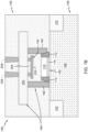
- FIG. 7A shows a Y cross-sectional view of fuse structure 100, according to another embodiment of the disclosure.
- FIG. 7A is similar to FIG. 6 , except resistor 232 is between metal wire 250 and fuse body 102, i.e., metal wire 250 is above resistor 232.
- Heater electrodes 234, 236 are routed to avoid metal wire 250, i.e., to the sides of metal wire 250, and metal contacts 142 of heat spreading structure 140 are routed to avoid resistor 232, i.e., to the sides of resistor 232.
- a thin dielectric layer 254 may separate resistor 232 and metal wire 250.
- resistor 232 heats metal wire 250 and the heat is transferred laterally over fuse body 102 and then vertically thereto by metal contacts 142.
- FIG. 7B shows a Y cross-sectional view of fuse structure 100 showing various landing arrangements of metal contacts 142 of heat spreading structure 140, according to alternative embodiments of the disclosure. While shown with the FIG. 7A embodiment, the various alternative embodiments of metal contacts 142 can be applied to any embodiment disclosed herein.
- metal contacts 142 of fuse structure 100 do not land on any structure, but simply pass next to spacers 112.
- metal contacts 142 may land on active region 106, i.e., they contact and stop on active region 106. (See also FIGS. 2 , 4 and 12-16 ).
- FIG. 7B shows a Y cross-sectional view of fuse structure 100 showing various landing arrangements of metal contacts 142 of heat spreading structure 140, according to alternative embodiments of the disclosure. While shown with the FIG. 7A embodiment, the various alternative embodiments of metal contacts 142 can be applied to any embodiment disclosed herein.
- metal contacts 142 of fuse structure 100 do not land on any structure, but simply pass next to spacers 112.
- metal contacts 142 may land on
- metal contacts 142 may at least partially land on spacer 112, e.g., depending on a width of spacer 112. While each drawing shows a particular landing arrangement for metal contacts 142, metal contacts 142 within a given heat spreading structure 140 and/or fuse structure 100 may include any landing arrangement. That is, metal contacts 142 within given heat spreading structure 140 and/or fuse structure 100 can have different landing arrangements.
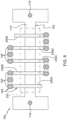
- FIGS. 8 and 9 show top-down views of fuse structure 100 according to another embodiment.
- FIGS. 8 and 9 are similar to FIGS. 6 and 7 , but in this embodiment, metal wire 250 of heat spreading structure 140 includes a plurality of metal wires 250A-E extending over fuse body 102. Each metal wire 250A-E may couple to at least a portion of the plurality of metal contacts 142, e.g., one or more of the metal contacts 142.
- metal heater 130 may include resistor 232 (shown in dashed lines to indicate it can be above or below metal wires 250A-E). While five metal wires 250A-E are shown arranged in a sinusoidal layout, any number of metal wires 250 may be used and may be coupled to any number of metal contacts 142 to provide the desired heat transfer to fuse body 102.
- FIGS. 8 and 9 also show a couple of the cross-sectional shape options, among others, of metal contacts 142.
- FIG. 8 shows a circular cross-section
- FIG. 9 shows a bar shaped cross-section.
- metal contacts 142 may become elongated elements 144 running parallel to fuse body 102.
- metal contacts 142 may also have a cross-sectional dimension configured to create the desired heating of fuse body 102.
- any number of metal contacts 142 may be used to create the desired heating of fuse body 102.
- metal contacts 142 are shown on both sides of fuse body 102, they may be used only on one side.
- FIG. 10 and 11 show top-down views of fuse structure 100 according to another embodiment.
- FIGS. 10 and 11 are similar to FIGS. 8 and 9 , except a metal wire 260 is not part of heat spreading structure 140, but part of metal heater 130.
- metal heater 130 as in FIGS. 1-3 , includes a plurality of metal wires 332A-E extending over fuse body 102. Each metal wire 332A-E may couple to a least a portion of metal contacts 142 of heat spreading structure 140.
- metal wires 332A-E While five metal wires 332A-E are shown arranged in a sinusoidal layout, any number of metal wires 332 may be used as part of metal heater 130, and may be coupled to any number of metal contacts 142 of heat spreading structure 140 to provide the desired heat transfer to fuse body 102.
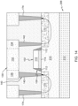
- FIGS. 12-14 show Y cross-sectional views of fuse structure 100, according to other embodiments of the disclosure. More particularly, FIGS. 12-14 show previous embodiments including additional heating features for heating fuse body 102.
- fuse structure 100 may include additional heating features in the form of a doped region 170 in substrate 108 below and to each side of fuse body 102 and a contact 174 landing on each doped region 170.
- Doped regions 170 are shown as n-type doped regions (n+), but they could be doped p-type depending on the type of transistors to be used elsewhere in IC structure 104. A portion of the plurality of metal contacts 142 land on each of the doped regions 170.
- FIG. 12 shows the additional heating features applied to the FIGS. 4-5 embodiment.
- FIG. 13 shows the additional heating feature applied to the FIGS. 4-5 embodiment, but including a semiconductor-on-insulator (SOI) substrate 208 application.
- SOI substrate 208 includes a semiconductor-on-insulator (SOI) layer (not shown) over a buried insulator layer 210 over a base semiconductor layer 212.
- FIG. 14 shows the additional heating features applied to the FIGS. 1-3 embodiment with an SOI substrate 208, like in FIG. 13 .
- current can be directed through one doped region 170 (left side) using contact 174 (left side) to heat fuse body 102 from underneath and to the side using doped region 170 (left side).
- Current can then pass vertically upward through metal contacts 142 to metal heater 130, through metal heater 130 (resistor 232 in FIGS. 12-13 , metal wire 132 in FIG. 14 ), and then vertically downward through metal contacts 142.
- Metal contacts 142 thus carry current and thermally communicate heat to fuse body 102 to/from metal heater 130.
- Current can pass from metal contacts 142 through the other doped region 170 (right side) to further heat fuse body 102 from underneath and to the side using doped region 170 (right side).
- Current can then pass out through contact 174 (right side). In this manner, the additional heating features of doped regions 170 can add more heat to fuse body 102.
- FIGS. 15-16 show Y cross-sectional views of fuse structure 100, according to other embodiments of the disclosure.
- FIGS. 15-16 show previous embodiments including additional heating features for heating fuse body 102.
- fuse structure 100 may include additional heating features in the form of additional metal contacts 274 landing on active region 106 to the sides of fuse body 102.
- FIG. 15 shows the additional metal contacts 274 applied to the FIGS. 2-3 embodiments.
- FIG. 16 shows the additional metal contacts 274 applied to the FIGS. 4-5 embodiment.
- current can be directed through one additional contact 274 (left side) to heat fuse body 102 from underneath and to the side using active region 106 (left side). Current can then pass vertically upward through metal contacts 142 to metal heater 130 (metal wire 132 in FIG.
- Metal contacts 142 thus carry current and thermally communicate heat to fuse body 102 from metal heater 130.
- Current can pass from metal contacts 142 through active region 106 (right side) to further heat fuse body 102 from underneath and to the side using active region 106 (right side).
- Current can then pass out through metal contact 274 (right side). In this manner, the additional heating features are provided using active region 106 to add more heat to fuse body 102.
- a method for heating a fuse in IC structure 104 may include heating an area over fuse body 102 using metal heater 130, and spreading heat from metal heater 130 through heat spreading structure 140 thermally coupled to metal heater 130 and extending horizontally adjacent to at least one side of fuse body 102.
- Embodiments of the disclosure provide various technical and commercial advantages, examples of which are discussed herein.
- Embodiments of the disclosure provide a fuse structure that reduces the necessary programming energy and also reduces the size of a programming current source, which will reduce the overall circuitry footprint. As described, the fuse structure does not require any additional masks to implement.
- the structure and method as described above are used in the fabrication of integrated circuit chips.
- the resulting integrated circuit chips can be distributed by the fabricator in raw wafer form (that is, as a single wafer that has multiple unpackaged chips), as a bare die, or in a packaged form.
- the chip is mounted in a single chip package (such as a plastic carrier, with leads that are affixed to a motherboard or other higher-level carrier) or in a multichip package (such as a ceramic carrier that has either or both surface interconnections or buried interconnections).
- the chip is then integrated with other chips, discrete circuit elements, and/or other signal processing devices as part of either (a) an intermediate product, such as a motherboard, or (b) an end product.
- the end product can be any product that includes integrated circuit chips, ranging from toys and other low-end applications to advanced computer products having a display, a keyboard or other input device, and a central processor.
- Approximating language may be applied to modify any quantitative representation that could permissibly vary without resulting in a change in the basic function to which it is related. Accordingly, a value modified by a term or terms, such as “about”, “approximately” and “substantially”, are not to be limited to the precise value specified. In at least some instances, the approximating language may correspond to the precision of an instrument for measuring the value.
- range limitations may be combined and/or interchanged, such ranges are identified and include all the sub-ranges contained therein unless context or language indicates otherwise. "Approximately” as applied to a particular value of a range applies to both values, and unless otherwise dependent on the precision of the instrument measuring the value, may indicate +/-10% of the stated value(s).
- the term "include” and its variants may be interpreted as meaning that an embodiment includes stated features, while not necessarily excluding the presence of other features that are not explicitly stated.
Landscapes
- Design And Manufacture Of Integrated Circuits (AREA)
Applications Claiming Priority (1)
| Application Number | Priority Date | Filing Date | Title |
|---|---|---|---|
| US18/064,472 US20240194592A1 (en) | 2022-12-12 | 2022-12-12 | Fuse structure with metal heater and heat spreading structure for fuse body |
Publications (1)
| Publication Number | Publication Date |
|---|---|
| EP4386830A1 true EP4386830A1 (de) | 2024-06-19 |
Family
ID=88290684
Family Applications (1)
| Application Number | Title | Priority Date | Filing Date |
|---|---|---|---|
| EP23201726.9A Pending EP4386830A1 (de) | 2022-12-12 | 2023-10-05 | Sicherungsstruktur mit metallischem heizer und wärmeverteilungsstruktur für sicherungskörper |
Country Status (3)
| Country | Link |
|---|---|
| US (1) | US20240194592A1 (de) |
| EP (1) | EP4386830A1 (de) |
| CN (1) | CN118198029A (de) |
Citations (4)
| Publication number | Priority date | Publication date | Assignee | Title |
|---|---|---|---|---|
| US20050029620A1 (en) * | 2003-08-07 | 2005-02-10 | Nec Electronics Corporation | Semiconductor device |
| US20070221966A1 (en) * | 2006-03-23 | 2007-09-27 | Taiwan Semiconductor Manufacturing Co., Ltd. | Method for integrally forming an electrical fuse device and a MOS transistor |
| CN104659013A (zh) * | 2013-11-19 | 2015-05-27 | 中芯国际集成电路制造(上海)有限公司 | 电熔丝结构及半导体器件 |
| CN109148414A (zh) * | 2017-06-13 | 2019-01-04 | 中芯国际集成电路制造(上海)有限公司 | 一种电可编程熔丝结构及电子装置 |
-
2022
- 2022-12-12 US US18/064,472 patent/US20240194592A1/en active Pending
-
2023
- 2023-10-05 EP EP23201726.9A patent/EP4386830A1/de active Pending
- 2023-10-23 CN CN202311372685.8A patent/CN118198029A/zh active Pending
Patent Citations (4)
| Publication number | Priority date | Publication date | Assignee | Title |
|---|---|---|---|---|
| US20050029620A1 (en) * | 2003-08-07 | 2005-02-10 | Nec Electronics Corporation | Semiconductor device |
| US20070221966A1 (en) * | 2006-03-23 | 2007-09-27 | Taiwan Semiconductor Manufacturing Co., Ltd. | Method for integrally forming an electrical fuse device and a MOS transistor |
| CN104659013A (zh) * | 2013-11-19 | 2015-05-27 | 中芯国际集成电路制造(上海)有限公司 | 电熔丝结构及半导体器件 |
| CN109148414A (zh) * | 2017-06-13 | 2019-01-04 | 中芯国际集成电路制造(上海)有限公司 | 一种电可编程熔丝结构及电子装置 |
Also Published As
| Publication number | Publication date |
|---|---|
| US20240194592A1 (en) | 2024-06-13 |
| CN118198029A (zh) | 2024-06-14 |
Similar Documents
| Publication | Publication Date | Title |
|---|---|---|
| US5744839A (en) | ESD protection using selective siliciding techniques | |
| US9184129B2 (en) | Three-terminal antifuse structure having integrated heating elements for a programmable circuit | |
| CN101814501B (zh) | 半导体装置 | |
| US7253064B2 (en) | Cascode I/O driver with improved ESD operation | |
| US7183612B2 (en) | Semiconductor device having an electrostatic discharge protecting element | |
| US10483383B2 (en) | Semiconductor device including a gate contact structure | |
| CN112951822B (zh) | 半导体器件 | |
| US4825280A (en) | Electrostatic discharge protection for semiconductor devices | |
| CN104979342A (zh) | 具有静电放电保护结构的半导体器件 | |
| JP7684922B2 (ja) | 半導体装置 | |
| US8486796B2 (en) | Thin film resistors and methods of manufacture | |
| US20240194592A1 (en) | Fuse structure with metal heater and heat spreading structure for fuse body | |
| US20250287689A1 (en) | Integrated circuit structure and method for manufacturing the same | |
| JP6930615B2 (ja) | 半導体装置 | |
| US20090253239A1 (en) | Method and structure for ballast resistor | |
| US20200118720A1 (en) | Tunable multi-segment thermistor | |
| TWI810899B (zh) | 熔絲結構 | |
| JP3204226B2 (ja) | 半導体装置 | |
| JP6246261B2 (ja) | 半導体装置 | |
| JP2906576B2 (ja) | 半導体装置 | |
| TWI919587B (zh) | 半導體裝置 | |
| JP2000040821A (ja) | 半導体装置の保護装置 | |
| JP3830871B2 (ja) | 静電放電保護素子 | |
| JP6894859B2 (ja) | 半導体装置 | |
| JPS62232965A (ja) | 半導体装置 |
Legal Events
| Date | Code | Title | Description |
|---|---|---|---|
| PUAI | Public reference made under article 153(3) epc to a published international application that has entered the european phase |
Free format text: ORIGINAL CODE: 0009012 |
|
| STAA | Information on the status of an ep patent application or granted ep patent |
Free format text: STATUS: REQUEST FOR EXAMINATION WAS MADE |
|
| 17P | Request for examination filed |
Effective date: 20231005 |
|
| AK | Designated contracting states |
Kind code of ref document: A1 Designated state(s): AL AT BE BG CH CY CZ DE DK EE ES FI FR GB GR HR HU IE IS IT LI LT LU LV MC ME MK MT NL NO PL PT RO RS SE SI SK SM TR |
|
| REG | Reference to a national code |
Ref country code: DE Ref legal event code: R079 Free format text: PREVIOUS MAIN CLASS: H01L0023340000 Ipc: H10W0020490000 |
|
| GRAP | Despatch of communication of intention to grant a patent |
Free format text: ORIGINAL CODE: EPIDOSNIGR1 |
|
| RIC1 | Information provided on ipc code assigned before grant |
Ipc: H10W 20/49 20260101AFI20260417BHEP Ipc: H10W 40/10 20260101ALI20260417BHEP |
|
| STAA | Information on the status of an ep patent application or granted ep patent |
Free format text: STATUS: GRANT OF PATENT IS INTENDED |
|
| INTG | Intention to grant announced |
Effective date: 20260527 |