EP4382984A1 - Linseneinheit, optisches system und vorrichtung zur messung spektraler eigenschaften - Google Patents
Linseneinheit, optisches system und vorrichtung zur messung spektraler eigenschaften Download PDFInfo
- Publication number
- EP4382984A1 EP4382984A1 EP22852993.9A EP22852993A EP4382984A1 EP 4382984 A1 EP4382984 A1 EP 4382984A1 EP 22852993 A EP22852993 A EP 22852993A EP 4382984 A1 EP4382984 A1 EP 4382984A1
- Authority
- EP
- European Patent Office
- Prior art keywords
- lens
- lens unit
- set forth
- optical system
- unit
- Prior art date
- Legal status (The legal status is an assumption and is not a legal conclusion. Google has not performed a legal analysis and makes no representation as to the accuracy of the status listed.)
- Pending
Links
Images













Classifications
-
- G—PHYSICS
- G02—OPTICS
- G02B—OPTICAL ELEMENTS, SYSTEMS OR APPARATUS
- G02B13/00—Optical objectives specially designed for the purposes specified below
- G02B13/14—Optical objectives specially designed for the purposes specified below for use with infrared or ultraviolet radiation
-
- G—PHYSICS
- G01—MEASURING; TESTING
- G01J—MEASUREMENT OF INTENSITY, VELOCITY, SPECTRAL CONTENT, POLARISATION, PHASE OR PULSE CHARACTERISTICS OF INFRARED, VISIBLE OR ULTRAVIOLET LIGHT; COLORIMETRY; RADIATION PYROMETRY
- G01J3/00—Spectrometry; Spectrophotometry; Monochromators; Measuring colours
- G01J3/02—Details
- G01J3/0205—Optical elements not provided otherwise, e.g. optical manifolds, diffusers, windows
- G01J3/0208—Optical elements not provided otherwise, e.g. optical manifolds, diffusers, windows using focussing or collimating elements, e.g. lenses or mirrors; performing aberration correction
-
- G—PHYSICS
- G01—MEASURING; TESTING
- G01J—MEASUREMENT OF INTENSITY, VELOCITY, SPECTRAL CONTENT, POLARISATION, PHASE OR PULSE CHARACTERISTICS OF INFRARED, VISIBLE OR ULTRAVIOLET LIGHT; COLORIMETRY; RADIATION PYROMETRY
- G01J3/00—Spectrometry; Spectrophotometry; Monochromators; Measuring colours
- G01J3/28—Investigating the spectrum
- G01J3/45—Interferometric spectrometry
- G01J3/453—Interferometric spectrometry by correlation of the amplitudes
- G01J3/4535—Devices with moving mirror
-
- G—PHYSICS
- G02—OPTICS
- G02B—OPTICAL ELEMENTS, SYSTEMS OR APPARATUS
- G02B13/00—Optical objectives specially designed for the purposes specified below
- G02B13/001—Miniaturised objectives for electronic devices, e.g. portable telephones, webcams, PDAs, small digital cameras
- G02B13/0015—Miniaturised objectives for electronic devices, e.g. portable telephones, webcams, PDAs, small digital cameras characterised by the lens design
- G02B13/002—Miniaturised objectives for electronic devices, e.g. portable telephones, webcams, PDAs, small digital cameras characterised by the lens design having at least one aspherical surface
- G02B13/003—Miniaturised objectives for electronic devices, e.g. portable telephones, webcams, PDAs, small digital cameras characterised by the lens design having at least one aspherical surface having two lenses
-
- G—PHYSICS
- G02—OPTICS
- G02B—OPTICAL ELEMENTS, SYSTEMS OR APPARATUS
- G02B13/00—Optical objectives specially designed for the purposes specified below
- G02B13/001—Miniaturised objectives for electronic devices, e.g. portable telephones, webcams, PDAs, small digital cameras
- G02B13/0015—Miniaturised objectives for electronic devices, e.g. portable telephones, webcams, PDAs, small digital cameras characterised by the lens design
- G02B13/002—Miniaturised objectives for electronic devices, e.g. portable telephones, webcams, PDAs, small digital cameras characterised by the lens design having at least one aspherical surface
- G02B13/0035—Miniaturised objectives for electronic devices, e.g. portable telephones, webcams, PDAs, small digital cameras characterised by the lens design having at least one aspherical surface having three lenses
-
- G—PHYSICS
- G02—OPTICS
- G02B—OPTICAL ELEMENTS, SYSTEMS OR APPARATUS
- G02B13/00—Optical objectives specially designed for the purposes specified below
- G02B13/001—Miniaturised objectives for electronic devices, e.g. portable telephones, webcams, PDAs, small digital cameras
- G02B13/008—Miniaturised objectives for electronic devices, e.g. portable telephones, webcams, PDAs, small digital cameras designed for infrared light
-
- G—PHYSICS
- G02—OPTICS
- G02B—OPTICAL ELEMENTS, SYSTEMS OR APPARATUS
- G02B13/00—Optical objectives specially designed for the purposes specified below
- G02B13/18—Optical objectives specially designed for the purposes specified below with lenses having one or more non-spherical faces, e.g. for reducing geometrical aberration
-
- G—PHYSICS
- G02—OPTICS
- G02B—OPTICAL ELEMENTS, SYSTEMS OR APPARATUS
- G02B27/00—Optical systems or apparatus not provided for by any of the groups G02B1/00 - G02B26/00, G02B30/00
- G02B27/0025—Optical systems or apparatus not provided for by any of the groups G02B1/00 - G02B26/00, G02B30/00 for optical correction, e.g. distorsion, aberration
-
- G—PHYSICS
- G02—OPTICS
- G02B—OPTICAL ELEMENTS, SYSTEMS OR APPARATUS
- G02B27/00—Optical systems or apparatus not provided for by any of the groups G02B1/00 - G02B26/00, G02B30/00
- G02B27/0025—Optical systems or apparatus not provided for by any of the groups G02B1/00 - G02B26/00, G02B30/00 for optical correction, e.g. distorsion, aberration
- G02B27/0037—Optical systems or apparatus not provided for by any of the groups G02B1/00 - G02B26/00, G02B30/00 for optical correction, e.g. distorsion, aberration with diffracting elements
-
- G—PHYSICS
- G02—OPTICS
- G02B—OPTICAL ELEMENTS, SYSTEMS OR APPARATUS
- G02B7/00—Mountings, adjusting means, or light-tight connections, for optical elements
- G02B7/02—Mountings, adjusting means, or light-tight connections, for optical elements for lenses
- G02B7/021—Mountings, adjusting means, or light-tight connections, for optical elements for lenses for more than one lens
-
- G—PHYSICS
- G02—OPTICS
- G02B—OPTICAL ELEMENTS, SYSTEMS OR APPARATUS
- G02B9/00—Optical objectives characterised both by the number of the components and their arrangements according to their sign, i.e. + or -
- G02B9/12—Optical objectives characterised both by the number of the components and their arrangements according to their sign, i.e. + or - having three components only
- G02B9/14—Optical objectives characterised both by the number of the components and their arrangements according to their sign, i.e. + or - having three components only arranged + - +
- G02B9/16—Optical objectives characterised both by the number of the components and their arrangements according to their sign, i.e. + or - having three components only arranged + - + all the components being simple
-
- G—PHYSICS
- G02—OPTICS
- G02B—OPTICAL ELEMENTS, SYSTEMS OR APPARATUS
- G02B9/00—Optical objectives characterised both by the number of the components and their arrangements according to their sign, i.e. + or -
- G02B9/34—Optical objectives characterised both by the number of the components and their arrangements according to their sign, i.e. + or - having four components only
Definitions
- the present invention relates to a lens unit, an optical system, and a spectral characteristic measurement device.
- Patent Literature 1 discloses a near-infrared spectral characteristic measurement device which includes an objective lens that collimates signal light from a specimen, a phase shifter that is provided in collimated light, and an imaging lens that causes an image of the specimen to be formed in a detecting section.
- Patent Literature 2 discloses an imaging system which includes an optical system (objective lens) that collimates light from an object, a plurality of imaging lenses that each cause an image to be formed in a detecting section with use of a part of collimated light, and filters that are provided to the respective plurality of imaging lenses.
- Patent Literature 2 also describes design of an objective lens for the visible region.
- spectral characteristic measurement devices such as a hyperspectral camera
- a lens unit is desired which is for configuring such a spectral characteristic measurement device, which can be used in a wavelength band of the infrared region, which can be applied to an objective lens, an imaging lens, or the like, and which has good resolution while sufficiently suppressing chromatic aberration.
- the object of the present invention is to provide (i) a lens unit that is for an infrared region and that has good resolution while sufficiently suppressing chromatic aberration, (ii) an optical system that includes the lens unit, and (iii) a spectral characteristic measurement device that includes the lens unit.
- a lens unit in accordance with an aspect of the present invention is a lens unit which includes a first lens, a second lens, and a third lens that are disposed in order and which is used for an infrared region that includes at least any one of wavelengths in a range of 7 pm to 14 pm, wherein an effective diameter of the first lens is larger than an effective diameter of the third lens, and an optical axis thickness of the third lens is greater than an optical axis thickness of any one of the first lens and the second lens.
- a lens unit in accordance with an aspect of the present invention has good resolution while sufficiently suppressing chromatic aberration.
- An optical system 1 in accordance with an embodiment is an optical system which can be used in a wavelength range of an infrared region (7 pm to 14 pm) and in which an image of an object plane T is formed on an image plane S on which an image sensor (detecting section) or the like can be disposed.
- Fig. 1 is a cross-sectional view that illustrates a configuration of a main part of the optical system 1 and that is along an optical axis. Note, here, that a cross-sectional view of an optical system 1 of Example 1 described later is illustrated as an example. Note that the infrared region means a region of wavelengths from 7 ⁇ m to 14 pm, unless otherwise specified.
- the optical system 1 includes a first lens unit 2 that is a lens unit in accordance with an aspect of the present invention, a second lens unit 3 that is a lens unit in accordance with an aspect of the present invention, and a diaphragm 4.
- the first lens unit 2 is an objective lens, and collimates light that has entered the first lens unit 2 from an object plane T side.
- the first lens unit 2 is configured such that a first lens L1, a second lens L2, and a third lens L3 are disposed in order from a diaphragm 4 side toward the object plane T side.
- the second lens unit 3 is an imaging lens that converges the collimated light on the image plane S, and is configured such that a first lens L1, a second lens L2, and a third lens L3 are disposed in order from a diaphragm 4 side toward an image plane S side.
- the second lens unit 3 has a configuration similar to that of the first lens unit 2.
- the second lens unit 3 is disposed so as to be bilaterally symmetrical to the first lens unit 2 with respect to the diaphragm 4.
- the diaphragm for each of these lens units is located to a collimated light side of the first lens L1.
- the diaphragm 4 for each of the units is configured so as to be shared.
- optical system 1 it is possible to apply the optical system 1 to a multispectral camera or a hyperspectral camera by, for example, disposing a filter or a phase shifter in a vicinity of the position of the diaphragm 4.
- the lens units are described below. Since the second lens unit 3 has a configuration similar to that of the first lens unit 2, the first lens unit 2 is described, unless otherwise specified.
- the first lens unit 2 is accommodated and fixed in a lens barrel 21.
- Fig. 2 is a cross-sectional view illustrating a state where the first lens unit 2 is accommodated and fixed in the lens barrel 21.
- Fig. 3 is a front view illustrating the first lens unit 2.
- the lens barrel 21 includes a first hole 22, a second hole 23, and a third hole 24.
- the third lens L3 is fitted in the first hole 22 in a state where the optical axis is aligned with the central axis of the lens barrel 21.
- the second hole 23 is connected to the first hole 22, and has a diameter larger than that of the first hole 22.
- the second lens L2 is fitted in the second hole 23 in a state where a first spacer 25 having a ring shape intervenes between the second lens L2 and the third lens L3.
- the first lens L1 is fitted in the second hole 23 in a state where a second spacer 26 having a ring shape intervenes between the first lens L1 and the second lens L2.
- the third hole 24 is connected to the second hole 23, and has a diameter larger than that of the second hole 23.
- a third spacer 27 having a ring shape is fitted in the third hole 24.
- a surface of the first lens L1 which surface is not in contact with the second spacer 26 is pressed by the third spacer 27.
- an aluminum alloy for example, A5052 or A5056
- Such an aluminum alloy may be subjected to a satin treatment (treatment for making asperities). Further, the aluminum alloy may be used in a state of being black anodized.
- the material of the lens barrel 21 is not limited to the aluminum alloy.
- the lens barrel 21 may be made of SUS304 (austenitic stainless steel), and black trivalent chromium plating may be applied to a surface layer.
- the effective diameter of the first lens L1 is larger than the effective diameter of the third lens L3.
- the optical axis thickness t3 of the third lens L3 is greater than the optical axis thickness of each of the first lens L1 and the second lens L2.
- the optical axis thickness t3 of the third lens L3 is preferably 0.5 times to 2 times a second distance d2 that is a distance on the optical axis between the second lens L2 and the third lens L3 (distance between respective surfaces of the second lens L2 and the third lens L3 which surfaces face each other).
- the optical system 1 has a high modulation transfer function (MTF) in each of a tangential direction and a sagittal direction at a spatial frequency of 41.7 cycles/mm.
- the spatial frequency of 41.7 cycles/mm corresponds to a Nyquist frequency f N of an image sensor having a pixel pitch of 12 pm.
- the first lens unit 2 (second lens unit 3) has such good resolution as to be used for an image sensor that is for an infrared region and that has a pixel pitch substantially equal to a wavelength. That the MTF at the above-described spatial frequency is high means having such good resolution as to be used for an image sensor that has a narrow pitch substantially equal to a wavelength.
- a first distance d1 that is a distance on the optical axis between the first lens L1 and the second lens L2 is preferably shorter than the second distance d2.
- a numerical aperture (NA) on an image side becomes higher, and it is possible to reduce the root mean square (RMS) radius of a concentrated spot on the image plane.
- the thickness of the first spacer 25 is preferably caused to be greater than the thickness of the second spacer 26. In this case, a tilt error is unlikely to occur when the lenses are assembled in the lens barrel.
- the ratio of the second distance d2 to the first distance d1 is preferably not more than 9.
- Examples of a material of each lens include germanium and chalcogenide glass.
- the chalcogenide glass contains 20% to 90% of tellurium (Te) by mol%, and preferably contains at least any one of 0% to 50% of germanium (Ge) and 0% to 50% of gallium (Ga).
- Absorption of light by the chalcogenide glass is very little over a wide wavelength range of the infrared region, i.e., a wavelength range of 7 pm to 14 pm, and tends to have a good internal transmittance at least in the above wavelength range.
- An internal transmittance refers to a transmittance inside the material, and does not include a reflection loss on a surface of the material.
- the chalcogenide glass is capable of achieving an internal transmittance of not less than 90%, particularly not less than 95%, at a wavelength of 10 pm.
- Such chalcogenide glass was developed by the applicant of the present application (see PCT International Publication, No. WO2020/105719A1 ).
- the Abbe number of the chalcogenide glass at a wavelength of 10 ⁇ m is preferably not less than 100 or not less than 150, and particularly preferably not less than 200.
- the Abbe number ( ⁇ 10) is calculated by an expression below.
- Application of the chalcogenide glass having the above Abbe number makes it possible to suppress chromatic aberration.
- v10 (refractive index at wavelenght of 10 ⁇ m - 1) / (refractive index at wavelength of 8 ⁇ m - refractive index at wavelength of 12 ⁇ m)
- the refractive index of the chalcogenide glass at a wavelength of 10 pm is preferably 2.5 to 4.0, 2.74 to 3.92, or 2.8 to 3.8, and particularly preferably 2.9 to 3.7.
- the refractive index is low, it is necessary to cause the radius of curvature of the lens to be smaller than that of a lens made of a material having a high refractive index. This is likely to result in an increase in the degree of difficulty in processing the lens.
- an optical degree of freedom is impaired, e.g., the thickness in the direction of the optical axis becomes greater.
- the chalcogenide glass preferably does not contain a toxic substance such as As, Se, or Tl. This makes it possible to reduce an environmental load.
- the third lens L3 is preferably made of a material which has, at a wavelength of 10 pm, an internal transmittance that is equal to or higher than the internal transmittance of a material of which the second lens L2 is made and that is equal to or higher than the internal transmittance of a material of which the first lens L1 is made.
- the above configuration causes an image formed by the optical system 1 to have good resolution.
- the internal transmittance of the material of which the third lens L3 is made is preferably not less than 90% and particularly preferably not less than 95% at a wavelength of 10 pm.
- the third lens L3 is preferably made of the above-described chalcogenide glass.
- the third lens L3 is preferably made of the chalcogenide glass having a refractive index of 2.5 to 4.0 at a wavelength of 10 pm.
- the above configuration causes an image formed by the optical system 1 to have good resolution.
- the second lens L2 is preferably made of the chalcogenide glass having a refractive index of 2.5 to 4.0 at a wavelength of 10 pm.
- the above configuration causes an image formed by the optical system 1 to have better resolution.
- the first lens L1 is preferably made of germanium. In this case, the first lens L1 has good durability and good hardness.
- Each lens of the first lens unit 2 (second lens unit 3) preferably has the following configuration.
- the first lens L1 preferably has positive power and has a meniscus shape in which a second lens L2 side of the first lens L1 is concave.
- the second lens L2 preferably has negative power.
- the third lens L3 preferably has positive power and has a meniscus shape in which a second lens L2 side of the third lens L3 is convex.
- the first lens L1 preferably has the diaphragm 4 that is located to a side of the first lens L1 which side is opposite from the second lens L2 in the direction of the optical axis.
- the ratio of the diameter of the diaphragm 4 to the effective diameter of an image is preferably 3 to 5 and more preferably 3 to 4.5. This configuration causes the NA on the image side to be high in the second lens unit 3, which is an imaging lens. Moreover, an NA on the object plane side becomes high in the first lens unit 2, which is an objective lens.
- At least one surface of the first lens L1 is preferably a spherical lens.
- the first lens L1 is often disposed at a position at which misalignment easily occurs. Therefore, the above configuration makes it easy to suppress occurrence of a tilt error.
- Both surfaces of the first lens L1 are more preferably spherical lenses.
- At least one surface of the second lens L2 or the third lens L3 is preferably an aspherical surface, or at least one surface of each of the second lens L2 and the third lens L3 is preferably an aspherical surface.
- the aspherical surface includes a diffraction surface.
- the second lens L2 and the third lens L3 are disposed at respective positions at each of which misalignment is unlikely to occur. Therefore, a tilt is unlikely to occur when each of the second lens L2 and the third lens L3 is mounted on the lens barrel 21.
- a surface of the third lens L3 which surface is located on a side opposite from a side that faces the second lens L2 is more preferably an aspherical surface.
- a surface of the second lens L2 which surface is located on a side that faces the third lens L3 is more preferably an aspherical surface.
- a surface of the second lens L2 which surface is located on a side that faces the first lens L1 may be an aspherical surface.
- the second lens L2 preferably has a diffraction surface. More specifically, at least one of the surface of the second lens L2 which surface is located on the side that faces the third lens L3 and the surface of the second lens L2 which surface is located on the side that faces the first lens L1 is preferably a diffraction surface. In this case, chromatic aberration is easily reduced. A level difference between a concave and a convex of the diffraction surface is preferably 1 pm to 10 ⁇ m. In this case, chromatic aberration is more easily suppressed.
- the NA on the image side preferably satisfies not less than 0.4.
- the NA on the image side is directly connected to resolution. Therefore, the resolution of the optical system 1 is improved.
- the MTF in the wavelength range of 7 ⁇ m to 14 ⁇ m at the spatial frequency of 41.7 cycles/mm satisfies preferably not less than 0.35 and particularly preferably not less than 0.40 in an image circle. This configuration causes the optical system 1 to have good resolution, resulting in good resolution on the image plane S.
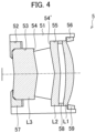
- FIG. 4 is a cross-sectional view illustrating a state where the lens unit 5 is accommodated and fixed in a lens barrel 51.
- the lens barrel 51 has a first hole 52, a second hole 53, a third hole 55, and a fourth hole 56.
- a third lens L3 is fitted in the first hole 52 and the second hole 53 in a state where an optical axis is aligned with the central axis of the lens barrel 51.
- a circumferential edge part of a surface of the third lens L3 which surface does not face a second lens L2 is pressed by a first spacer 57 having a ring shape.
- the first spacer 57 having a ring shape is fitted in the first hole 52.
- the second hole 53 is connected to the first hole 52, and has a diameter smaller than that of the first hole 52.
- the second hole 53 has a protruding part 54 that engages with a circumferential edge part of a surface of the third lens L3 which surface is not in contact with the first spacer 57.
- the third hole 55 is connected to the second hole 53, and has a diameter larger than that of the second hole 53.
- the third hole 55 has a protruding part 54' that engages with a circumferential edge part of a surface of the second lens L2 which surface is not in contact with a second spacer 58.
- the second lens L2, the second spacer 58 having a ring shape, and a first lens L1 are fitted in the third hole 55 in order.
- the fourth hole 56 is connected to the third hole 55, and has a diameter larger than that of the third hole 55.
- a third spacer 59 having a ring shape is fitted in the fourth hole 56.
- the third spacer 59 presses a circumferential edge part of a surface of the first lens L1 which surface is not in contact with the second spacer 58.
- At least one surface of the second lens L2 or the third lens L3 is preferably an aspherical surface, or at least one surface of each of the second lens L2 and the third lens L3 is preferably an aspherical surface.
- the second lens L2 and the third lens L3 are disposed at respective positions at each of which misalignment is unlikely to occur. Therefore, a tilt is unlikely to occur when each of the second lens L2 and the third lens L3 is mounted on the lens barrel 51.
- the second lens L2 and the third lens L3 has an aspherical surface
- a reduction in an MTF and an expansion of an RMS radius which reduction and expansion are caused by occurrence of a tilt are unlikely to occur, and also aberration is easily suppressed.
- at least one of respective surfaces of the second lens L2 and the third lens L3 which surfaces face each other is more preferably an aspherical surface. In this case, a deterioration of resolution which deterioration is caused by a slight tilt error or decenter error during assembly of the lenses is unlikely to be induced.
- Fig. 5 is a cross-sectional view illustrating a spectral characteristic measurement device 10 to which lens units in accordance with an embodiment are applied.
- the spectral characteristic measurement device 10 includes a first lens unit 2, a second lens unit 3, a sample support plate 6, a detecting section 7, and a phase shifter 8.
- the configurations of the first lens unit 2 and the second lens unit 3 of the spectral characteristic measurement device 10 are similar to those of the first lens unit 2 and the second lens unit 3 of the optical system 1.
- a third lens L3 of the first lens unit 2 is disposed so as to face the sample support plate 6, and a third lens L3 of the second lens unit 3 is disposed so as to face the detecting section 7.
- the phase shifter 8 is disposed between the first lens unit 2 and the second lens unit 3.
- the optical axis of the first lens unit 2 and the optical axis of the second lens unit 3 are perpendicular to each other in the phase shifter 8.
- the optical axis is bent perpendicularly in the phase shifter 8 of a reflection type.
- a basic optical configuration is the same as that of the above-described optical system 1 of a transmission type.
- the phase shifter 8 is disposed in a vicinity of the position of a diaphragm 4 of the optical system 1. That is, the first lens unit 2 and the second lens unit 3 are disposed symmetrically with respect to the phase shifter 8.
- the spectral characteristic measurement device 10 employs the phase shifter 8 of a reflection type.
- the phase shifter 8 includes a fixed mirror section 81, a movable mirror section 82, and a driving section 83.
- the fixed mirror section 81 and the movable mirror section 82 are disposed so as to be arranged in the direction perpendicular to the drawing surface of Fig. 5 (direction of an x axis) in a state where the movable mirror section 82 is located on a far side of the direction of the x axis with respect to the fixed mirror section 81.
- the fixed mirror section 81 and the movable mirror section 82 are disposed so as to be tilted ⁇ degrees (approximately 45 degrees) with respect to the optical axis of the first lens unit 2. That is, the fixed mirror section 81 and the movable mirror section 82 are disposed so as to be tilted ⁇ degrees (approximately 45 degrees) with respect to the optical axis of the second lens unit 3.
- the movable mirror section 82 is configured such that the movable mirror section 82 can be moved in the direction perpendicular to a surface of the movable mirror section 82.
- phase shifter 8 is not limited the reflection type, and may be of a transmission type.
- Infrared light is emitted from a light source (not illustrated) toward a sample (not illustrated) in a state where the sample is supported on the sample support plate 6.
- the infrared light is scattered by various components of the sample, and the scattered light enters the third lens L3 of the first lens unit 2.
- the scattered light is caused to be a collimated light beam by the first lens unit 2.
- the collimated light beam reaches the fixed mirror section 81 and the movable mirror section 82 of the phase shifter 8. A part of the light is reflected by the fixed mirror section 81, and enters a first lens L1 of the second lens unit 3 as a first light beam.
- the remaining part of the light is reflected by the movable mirror section 82, and enters the first lens L1 of the second lens unit 3 as a second light beam.
- the first light beam and the second light beam that have entered the second lens unit 3 cause an image to be formed on a light receiving surface of the detecting section 7, so that an interference image is formed.
- a waveform of an interferogram (change in imaging intensity (change in intensity of interference light)) is obtained.
- a spectral characteristic of the sample is obtained.
- the spectral characteristic measurement device 10 includes lens units of an aspect of the present invention. Therefore, an image formed in the detecting section 7 has good resolution. This makes it possible to obtain a waveform of a clear and well resolved interferogram.
- a lens unit of Example 1 is the first lens unit or the second lens unit 3 illustrated in Fig. 1 .
- the second lens unit 3 is described below.
- the first lens unit also has the same configuration.
- Tables 1 and 2 below respectively show basic lens data and aspherical surface data of the second lens unit 3 of Example 1.
- chalcogenide glass used in the examples and the comparative examples below has a refractive index of 3.465 at a wavelength of 10 ⁇ m and an Abbe number ⁇ 10 of 253.
- Germanium has a refractive index of 4.004 at wavelength of 10 pm and an Abbe number ⁇ 10 of 942.
- an infrared sensor detecting section 7 having a pitch of 12 pm was premised.
- Example 1 Basic lens data Surface number Radius of curvature Distance Material Effective diameter 1 (Diaphragm) ⁇ 40.00 32.0 2 55.380 6.00 G 46.4 3 110.945 4.00 44.0 4 123.082 4.50 CH 41.0 5* 67.226 13.00 39.0 6 45.300 18.00 CH 31.0 7 41.447 9.00 20.0 Image plane ⁇ 9.6
- a first lens L1 of the second lens unit 3 is made of germanium, and a second lens L2 and a third lens L3 each employ chalcogenide glass.
- the optical axis thickness t3 of the third lens L3 is greater than the optical axis thickness of each of the first lens L1 and the second lens L2.
- the effective diameter of the first lens L1 is larger than the effective diameter of the third lens L3.
- Table 3 shows t3/cps, t3/d2, d2/d1, cpa/cps, an F-number, f, and an NA of the second lens unit 3 of Example 1.
- Table 3 further shows results of MTFs and spot diagrams of an optical system 1 of Example 1 which optical system 1 employs lens units of Example 1 as an objective lens (first lens unit 2) and an imaging lens (second lens unit 3).
- the "t3" represents the thickness of the third lens L3 in the direction of the optical axis (distance shown in the row “Surface 6" of the basic lens data)
- the “ ⁇ s” represents the effective diameter of the image plane S
- the "d2” represents a distance on the optical axis between the second lens L2 and the third lens L3 (distance shown in the row “Surface 5" of the basic lens data)
- the "d1” represents a distance on the optical axis between the first lens L1 and the second lens L2 (distance shown in the row “Surface 3" of the basic lens data)
- the " ⁇ a” represents the diameter of an aperture diaphragm.
- Example 1 1.88 1.38 3.25 3.33 1.16 37.2 0.430 0.412 good
- Example 2 1.88 1.29 7.00 3.43 1.09 36.1 0.458 0.441 good
- Example 3 1.88 0.82 7.33 3.33 1.12 35.7 0.448 0.446 good
- Example 4 1.88 0.82 7.33 3.33 1.20 38.2 0.418 0.369 good
- Example a 2.60 0.89 8.00 3.33 1.20 38.2 0.419 0.371 good
- Example 6 2.60 0.89 8.00 3.34 1.19 38.1 0.420 0.409 good
- Example 7 3.54 9.44 0.72 4.36 1.17 49.1 0.428 0.352 good
- Example 8 1.88 1.38 3.25 4.83 1.10 35.2 0.453 0.444 good
- Example 9 1.49 0.79 4.50 3.
- the total length (sum of distances between surfaces) of the optical system 1 of Example 1 is 189 mm.
- the NA of the second lens unit 3 of Example 1 exceeds 0.4.
- the second lens unit 3 of Example 1 is suitable for a hyperspectral camera, and also is applicable to various optical systems.
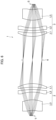
- Fig. 6 is a ray diagram obtained by illustrating optical paths on a cross-sectional view of a main part of the optical system 1 of Example 1 which optical system 1 employs the lens units of Example 1 as an objective lens (first lens unit 2) and an imaging lens (second lens unit 3).
- Fig. 7 is a graph showing spatial frequency dependence of the MTFs of the optical system 1 of Example 1 in a wavelength range of 7 pm to 14 pm.
- the MTFs in a tangential direction and a sagittal direction are shown.
- the Nyquist frequency f N of an image sensor having a pixel pitch of 12 pm is 41.7 cycles/mm.
- the MTFs of the optical system 1 of Example 1 are each not less than 0.35 at a spatial frequency of 41.7 cycles/mm. Therefore, the optical system 1 of Example 1 has good MTFs. Thus, it is found that good resolution that allows use for an image sensor having a narrow pitch substantially equal to a wavelength is obtained.
- Table 3 shows an MTF at the spatial frequency of 41.7 cycles/mm.
- Table 3 shows a minimum one of values in the tangential direction and the sagittal direction regarding light beams emitted from object heights.
- the object heights Y are 0.00 mm, 1.20 mm, 2.40 mm, 3.60 mm, and 4.80 mm.
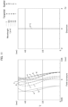
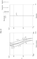
- the left side of Fig. 8 is a graph showing, by millimeter, shift amounts (field curvatures) in the tangential direction and the sagittal direction in the wavelength range of 7 pm to 14 pm.
- the right side of Fig. 8 is a graph showing, by percentage, distortions in the tangential direction at each wavelength.
- a through j each represent a field curvature and a distortion in the tangential direction or the sagittal direction at a wavelength of 7 pm, 8.5 pm, 10 pm, 12 pm, or 14 pm.
- the shift amounts in the tangential direction and the sagittal direction in the wavelength range of 7 pm to 14 pm are small.
- the distortions in the tangential direction and the sagittal direction in the wavelength range of 7 pm to 14 pm are extremely small and close to 0%.
- optical system 1 has good characteristics (resolution, aberration characteristics) indicates that the first lens unit 2 and the second lens unit 3 have excellent characteristics.
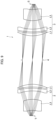
- Fig. 9 is a ray diagram obtained by illustrating optical paths on a cross-sectional view of a main part of an optical system 1 of Example 2.
- Tables 4 and 5 respectively show basic lens data and aspherical surface data of a second lens unit 3 of Example 2.
- Table 3 above shows t3/ ⁇ s, t3/d2, d2/d1, ⁇ a/ ⁇ s, an F-number, f, and an NA of the second lens unit 3 of Example 2.
- Table 3 above further shows results of MTFs and spot diagrams of the optical system 1 of Example 2 which optical system 1 employs lens units of Example 2 as an objective lens (first lens unit 2) and an imaging lens (second lens unit 3).
- the total length of the optical system 1 of Example 2 is 184 mm.
- Example 2 Basic lens data Surface number Radius of curvature Distance Material Effective diameter 1 (Diaphragm) ⁇ 40.00 33.0 2 53.611 4.50 G 46.4 3 107.812 2.00 44.0 4 109.466 4.50 CH 44.0 5* 67.355 14.00 41.0 6 45.903 18.00 CH 29.8 7 39.846 9.00 18.8 Image plane ⁇ 9.6 [Table 5] Example 2 Aspherical surface data Coefficient Fifth surface ⁇ 0 A2 0 A4 7.127535E-07 A6 1.263693E-10 A8 0 A10 0
- Fig. 10 is a graph showing spatial frequency dependence of the MTFs in a wavelength range of 7 pm to 14 pm. According to Fig. 10 , the MTFs of the optical system 1 of Example 2 are each not less than 0.35 at a spatial frequency of 41.7 cycles/mm.
- the left side of Fig. 11 is a graph showing, by millimeter, shift amounts (field curvatures) in a tangential direction and a sagittal direction in the wavelength range of 7 pm to 14 pm.
- the right side of Fig. 11 is a graph showing, by percentage, distortions in the tangential direction at each wavelength. According to Fig. 11 , the shift amounts in the tangential direction and the sagittal direction in the wavelength range of 7 pm to 14 pm are small. Further, the distortions in the tangential direction and the sagittal direction in the wavelength range of 7 pm to 14 pm are extremely small and close to 0%. Thus, it is found that, in the optical system 1 of Example 2, aberration is suppressed.
- Fig. 12 is a ray diagram obtained by illustrating optical paths on a cross-sectional view of a main part of an optical system 1 of Example 3.
- Tables 6 and 7 respectively show basic lens data and aspherical surface data of a second lens unit 3 of Example 3.
- Table 3 above shows t3/ ⁇ s, t3/d2, d2/d1, ⁇ a/ ⁇ s, an F-number, f, and an NA of the second lens unit 3 of Example 3.
- Table 3 above further shows results of MTFs and spot diagrams of the optical system 1 of Example 3 which optical system 1 employs lens units of Example 3 as an objective lens (first lens unit 2) and an imaging lens (second lens unit 3).
- the total length of the optical system 1 of Example 3 is 195 mm.
- Example 3 Basic lens data Surface number Radius of curvature Distance Material Effective diameter 1 (Diaphragm) ⁇ 37.00 32.0 2 59.280 4.50 G 43.7 3 123.252 3.00 42.6 4* 1020.944 4.00 CH 41.0 5* 117.297 22.00 39.3 6* 34.314 18.00 CH 33.0 7* 33.356 9.00 20.1 Image plane ⁇ 9.6 [Table 7] Example 3 Aspherical surface data Coefficient Fourth surface Fifth surface Sixth surface Seventh surface ⁇ 0 0 0 0 A2 0 0 0 0 A4 3.356928E-07 2.440322E-07 1.819963E-07 3.221109E-06 A6 -4.507063E-11 -4.444816E-11 8.134734E-12 -8.676762E-09 A8 -1.845401E-13 -2.842570E-13 4.476816E-13 1.805166E-11 A10 0 0 -2.316204E-15 -3.316243E-13
- Fig. 13 is a graph showing spatial frequency dependence of the MTFs in a wavelength range of 7 pm to 14 pm. According to Fig. 13 , the MTFs of the optical system 1 of Example 3 are each not less than 0.35 at a spatial frequency of 41.7 cycles/mm.
- the left side of Fig. 14 is a graph showing, by millimeter, shift amounts (field curvatures) in a tangential direction and a sagittal direction in the wavelength range of 7 ⁇ m to 14 pm.
- the right side of Fig. 14 is a graph showing, by percentage, distortions in the tangential direction at each wavelength.
- the shift amounts in the tangential direction and the sagittal direction in the wavelength range of 7 pm to 14 pm are small.
- the distortions in the tangential direction and the sagittal direction in the wavelength range of 7 pm to 14 pm are extremely small and close to 0%.
- Fig. 15 is a ray diagram obtained by illustrating optical paths on a cross-sectional view of a main part of an optical system 1 of Example 4.
- Table 8 shows basic lens data of Example 4.
- Table 3 above shows t3/cps, t3/d2, d2/d1, cpajcps, an F-number, f, and an NA of a second lens unit 3 of Example 4.
- Table 3 above further shows results of MTFs and spot diagrams of the optical system 1 of Example 4 which optical system 1 employs lens units of Example 4 as an objective lens (first lens unit 2) and an imaging lens (second lens unit 3). Lenses of the second lens unit 3 of Example 4 do not have an aspherical surface.
- the total length of the optical system 1 of Example 4 is 195 mm.
- Fig. 16 is a ray diagram obtained by illustrating optical paths on a cross-sectional view of a main part of an optical system 1 of Example 5.
- Tables 9 and 10 respectively show basic lens data and aspherical surface data of a second lens unit 3 of Example 5.
- Table 3 above shows t3/ ⁇ s, t3/d2, d2/d1, ⁇ a/ ⁇ s, an F-number, f, and an NA of the second lens unit 3 of Example 5.
- Table 3 above further shows results of MTFs and spot diagrams of the optical system 1 of Example 5 which optical system 1 employs lens units of Example 5 as an objective lens (first lens unit 2) and an imaging lens (second lens unit 3).
- the total length of the optical system 1 of Example 5 is 245 mm.
- Example 5 Basic lens data Surface number Radius of curvature Distance Material Effective diameter 1 (Diaphragm) ⁇ 50.00 32.0 2 61.170 4.50 G 46.9 3 106.810 3.50 45.6 4* 315.372 4.50 CH 44.0 5* 114.806 28.00 42.0 6* 40.822 25.00 CH 34.1 7* 37.615 7.00 18.3 Image plane ⁇ 9.6 [Table 10] Example 5 Aspherical surface data Coefficient Fourth surface Fifth surface Sixth surface Seventh surface ⁇ 0 0 0 0 A2 0 0 0 0 A4 2.582082E-07 3.126138E-07 -4.425896E-07 -5.608176E-06 A6 -7.594670E-10 -9.626130E-10 -3.066738E-10 -9.457386E-09 A8 1.795998E-12 2.645816E-12 8.195477E-13 4.929964E-11 A10 -2.017857E-15 -3.303396E-15 -2
- Fig. 17 is a ray diagram obtained by illustrating optical paths on a cross-sectional view of a main part of an optical system 1 of Example 6.
- Tables 11 and 12 respectively show basic lens data and aspherical surface data of a second lens unit 3 of Example 6.
- Table 3 above shows t3/ ⁇ s, t3/d2, d2/d1, ⁇ a/ ⁇ s, an F-number, f, and an NA of the second lens unit 3 of Example 7.
- Table 3 above further shows results of MTFs and spot diagrams of the optical system 1 of Example 6 which optical system 1 employs lens units of Example 6 as an objective lens (first lens unit 2) and an imaging lens (second lens unit 3).
- the total length of the optical system 1 of Example 6 is 245 mm.
- Example 6 Basic lens data Surface number Radius of curvature Distance Material Effective diameter 1 (Diaphragm) ⁇ 50.00 32.0 2 59.843 4.50 G 47.0 3 102.735 3.50 45.7 4* 280.377 4.50 CH 44.1 5* 108.216 28.00 42.1 6* 40.720 25.00 CH 34.2 7* 38.028 7.00 18.3 Image plane ⁇ 9.6 [Table 12] Example 6 Aspherical surface data Coefficient Fourth surface Fifth surface Sixth surface Seventh surface ⁇ 0 0 0 0 A2 0 0 0 0 A4 -1.574997E-07 -1.897424E-07 -5.145472E-07 -5.338938E-06 A6 0 0 -6.439937E-11 -2.240402E-09 A8 0 0 0 0 0 0 0 0 0 0
- Fig. 18 is a ray diagram obtained by illustrating optical paths on a cross-sectional view of a main part of an optical system 1 of Example 7.
- Tables 13 and 14 respectively show basic lens data and aspherical surface data of a second lens unit 3 of Example 7.
- Table 3 above shows t3/ ⁇ s, t3/d2, d2/d1, ⁇ a/ ⁇ s, an F-number, f, and an NA of the second lens unit 3 of Example 7.
- Table 3 above further shows results of MTFs and spot diagrams of the optical system 1 of Example 7 which optical system 1 employs lens units of Example 7 as an objective lens (first lens unit 2) and an imaging lens (second lens unit 3).
- the total length of the optical system 1 of Example 7 is 213.4 mm.
- Example 7 Basic lens data Surface number Radius of curvature Distance Material Effective diameter 1 (Diaphragm) ⁇ 30.00 42.0 2 188.967 4.50 CH 47.3 3 457.694 5.00 46.9 4* 71.196 3.60 CH 45.2 5* 45.508 3.60 42.4 6 57.013 34.00 G 44.9 7 97.160 26.00 31.0 Image plane ⁇ 9.6 [Table 14] Example 7 Aspherical surface data Coefficient Fourth surface Fifth surface ⁇ 0 0 A2 0 0 A4 3.417494E-07 5.034096E-07 A6 0 0 A8 0 0 A10 0 0 0
- Fig. 19 is a ray diagram obtained by illustrating optical paths on a cross-sectional view of a main part of an optical system 1 of Example 8.
- Tables 15, 16, and 17 show basic lens data and diffraction surface data of a second lens unit 3 of Example 8.
- Table 3 above shows t3/ ⁇ s, t3/d2, d2/d1, ⁇ a/ ⁇ s, an F-number, f, and an NA of the second lens unit 3 of Example 8.
- Table 3 above further shows results of MTFs and spot diagrams of the optical system 1 of Example 8 which optical system 1 employs lens units of Example 8 as an objective lens (first lens unit 2) and an imaging lens (second lens unit 3).
- the total length of the optical system 1 of Example 8 is 189 mm.
- Example 8 Basic lens data Surface number Radius of curvature Distance Material Effective diameter 1 (Diaphragm) ⁇ 40.00 32.0 2 42.652 6.00 G 46.4 3 41.730 4.00 44.0 4* (Diffraction surface) 50.850 4.50 CH 41.0 5 69.889 13.00 39.0 6 44.326 18.00 CH 31.0 7 37.765 9.00 20.0 Image plane ⁇ 9.6
- Example 8 As shown in Table 15, in Example 8, a first lens L1 is made of germanium, and a second lens L2 and a third lens L3 are each made of chalcogenide glass. A fourth surface of the second lens L2 is a diffraction surface.
- Example 8 Aspherical surface data Coefficient Fourth surface ⁇ 0 A2 0 A4 -6.421421E-07 A6 -3.278357E-10 A8 0 A10 0
- Example 8 Diffraction surface data Coefficient Fourth surface P1 -696.16961 P2 -57.56012
- ⁇ P 1 ⁇ h / h n 2 + P 2 ⁇ h / h n 4
- Fig. 20 is a graph showing spatial frequency dependence of the MTFs in a wavelength range of 7 pm to 14 pm. According to Fig. 20 , the MTFs of the optical system 1 of Example 8 are each not less than 0.35 at a spatial frequency of 41.7 cycles/mm.
- the left side of Fig. 21 is a graph showing, by millimeter, field curvatures in a tangential direction and a sagittal direction in the wavelength range of 7 pm to 14 pm.
- the right side of Fig. 21 is a graph showing, by percentage, distortions in the tangential direction at each wavelength. According to Fig. 21 , shift amounts in the tangential direction and the sagittal direction in the wavelength range of 7 pm to 14 pm are small. Further, the distortions in the tangential direction and the sagittal direction in the wavelength range of 7 pm to 14 pm are extremely small and close to 0%. Thus, it is found that, in the optical system 1 of Example 8, aberration is suppressed.
- Fig. 22 is a ray diagram obtained by illustrating optical paths on a cross-sectional view of a main part of an optical system 1 of Example 9.
- Tables 18, 19, and 20 show basic lens data and diffraction surface data of a second lens unit 3 of Example 9.
- Table 3 above shows t3/ ⁇ s, t3/d2, d2/d1, ⁇ a/ ⁇ s, an F-number, f, and an NA of the second lens unit 3 of Example 9.
- Table 3 above further shows results of MTFs and spot diagrams of the optical system 1 of Example 9 which optical system 1 employs lens units of Example 9 as an objective lens (first lens unit 2) and an imaging lens (second lens unit 3).
- the total length of the optical system 1 of Example 9 is 191.6 mm.
- Example 9 As shown in Table 18, in Example 9, a first lens L1 is made of germanium, and a second lens L2 and a third lens L3 are each made of chalcogenide glass. A fifth surface of the second lens L2 is a diffraction surface.
- Example 9 Aspherical surface data Coefficient Fifth surface ⁇ 0 A2 0 A4 5.399270E-07 A6 1.168815E-11 A8 0 A10 0
- Example 9 Diffraction surface data Coefficient Fifth surface P1 -943.69016 P2 392.78661
- Fig. 23 is a graph showing spatial frequency dependence of the MTFs in a wavelength range of 7 pm to 14 pm. According to Fig. 23 , the MTFs of the optical system 1 of Example 9 are each not less than 0.35 at a spatial frequency of 41.7 cycles/mm.
- the left side of Fig. 24 is a graph showing, by millimeter, field curvatures in a tangential direction and a sagittal direction in the wavelength range of 7 pm to 14 pm.
- the right side of Fig. 24 is a graph showing, by percentage, distortions in the tangential direction at each wavelength. According to Fig. 24 , shift amounts in the tangential direction and the sagittal direction in the wavelength range of 7 pm to 14 pm are small. Further, the distortions in the tangential direction and the sagittal direction in the wavelength range of 7 pm to 14 pm are extremely small and close to 0%. Thus, it is found that, in the optical system 1 of Example 9, aberration is suppressed.
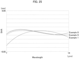
- Fig. 25 is a graph showing axial chromatic aberration in the wavelength range of 7 pm to 14 pm with regard to Examples 1, 8, and 9. It is found that, as compared with Example 1 which does not have a diffraction surface, Examples 8 and 9 each of which has a diffraction surface have improved axial chromatic aberration.
- Fig. 26 is a ray diagram obtained by illustrating optical paths on a cross-sectional view of a main part of an optical system of Comparative Example 1.
- Tables 21 and 22 respectively show basic lens data and aspherical surface data of a second lens unit of Comparative Example 1.
- Table 3 above shows t3/ ⁇ s, t3/d2, d2 / d 1, ⁇ a/ ⁇ s, an F-number, f, and an NA of the second lens unit of Comparative Example 1.
- Table 3 above further shows results of MTFs and spot diagrams of the optical system of Comparative Example 1 which optical system employs lens units of Comparative Example 1 as an objective lens (first lens unit) and an imaging lens (second lens unit).
- the total length of the optical system of Comparative Example 1 is 244 mm.
- a first lens L1 and a third lens L3 are each made of germanium, and a second lens L2 is made of chalcogenide glass.
- the optical axis thickness of the second lens L2 is greater than the optical axis thickness of each of the first lens L1 and the third lens L3, and the effective diameter of the first lens L1 is larger than the effective diameter of the third lens L3.
- Fig. 27 is a ray diagram obtained by illustrating optical paths on a cross-sectional view of a main part of an optical system 1 of Comparative Example 2.
- Tables 23 and 24 respectively show basic lens data and aspherical surface data of a second lens unit of Comparative Example 2.
- Table 3 above shows t3/ ⁇ s, t3/d2, d2 / d 1, ⁇ a/ ⁇ s, an F-number, f, and an NA of the second lens unit of Comparative Example 2.
- Table 3 above further shows results of MTFs and spot diagrams of the optical system of Comparative Example 2 which optical system employs lens units of Comparative Example 2 as an objective lens (first lens unit) and an imaging lens (second lens unit).
- the total length of the optical system of Comparative Example 2 is 252 mm.
- a third lens L3 is made of germanium, and a first lens L1 and a second lens L2 are each made of chalcogenide glass.
- the optical axis thickness of the first lens L1 is greater than the optical axis thickness of each of the second lens L2 and the third lens L3, and the effective diameter of the first lens L1 is larger than the effective diameter of the third lens L3.
- Fig. 28 is a ray diagram obtained by illustrating optical paths on a cross-sectional view of a main part of an optical system 1 of Comparative Example 3.
- Tables 25 and 26 respectively show basic lens data and aspherical surface data of a second lens unit of Comparative Example 3.
- Table 3 above shows t3/ ⁇ s, t3/d2, d2/d1, ⁇ a/ ⁇ s, an F-number, f, and an NA of the second lens unit of Comparative Example 3.
- Table 3 above further shows results of MTFs and spot diagrams of the optical system of Comparative Example 3 which optical system employs lens units of Comparative Example 3 as an objective lens (first lens unit) and an imaging lens (second lens unit 3).
- the total length of the optical system of Comparative Example 3 is 145.9 mm.
- a first lens L1 is made of germanium, and a second lens L2 and a third lens L3 are each made of chalcogenide glass.
- the optical axis thickness of the first lens L1 is greater than the optical axis thickness of each of the second lens L2 and the third lens L3, and the effective diameter of the first lens L1 is larger than the effective diameter of the third lens L3.
- the optical systems 1 of Examples 1 through 9 each have a high NA on the image side and have good resolution while aberration is suppressed. Moreover, it was confirmed that the optical systems 1 of Examples 1 through 9 each have a high MTF at the spatial frequency of 41.7 cycles/mm and have such good resolution as to be used for an image sensor having a pixel pitch of approximately 12 pm. Therefore, in a case where each of the optical systems 1 in accordance with the examples of the present invention is applied to a spectral characteristic measurement device 10, it is possible to obtain a waveform of a clear and well resolved interferogram.
- the optical axis thickness of the second lens L2 is greater than the optical axis thickness of each of the first lens L1 and the third lens L3.
- the optical axis thickness of the first lens L1 is greater than the optical axis thickness of each of the second lens L2 and the third lens L3. Therefore, the NA on the image side of each of the optical systems of Comparative Examples 1 and 3 is less than 0.4, and the MTF at the spatial frequency of 41.7 cycles/mm of each of the optical systems of Comparative Examples 1 through 3 is lower than 0.35.
- each of the optical systems of Comparative Examples 1 through 3 has poor resolution, and it is not possible to obtain a waveform of a clear interferogram in a case where each of the optical systems of Comparative Examples 1 through 3 is applied to a spectral characteristic measurement device 10.
- Example 7 By a comparison of Examples 1 through 6, 8, and 9 with Example 7, it is found that a higher MTF is obtained in a case where the third lens L3 is made of chalcogenide glass than in a case where the third lens L3 is made of germanium. Further, t3/d2 is preferably 0.5 to 2, and d2/d1 is preferably higher than 1.
- d2/d1 is preferably not more than 9.
- t3/cps is preferably 1 to 4
- ⁇ a/ ⁇ s is preferably 3 to 5 and more preferably 3 to 4.5.
- Example 8 and 9 As described above, as compared with Example 1 which does not have a diffraction surface, Examples 8 and 9 each of which has a diffraction surface have improved axial chromatic aberration.
- a lens unit in accordance with a first aspect of the present invention is a lens unit which includes a first lens, a second lens, and a third lens that are disposed in order and which is used for an infrared region that includes at least any one of wavelengths in a range of 7 pm to 14 pm, wherein an effective diameter of the first lens is larger than an effective diameter of the third lens, and an optical axis thickness of the third lens is greater than an optical axis thickness of any one of the first lens and the second lens.
- the lens unit has good resolution. In a case where the lens unit is applied to a spectral characteristic measurement device, it is possible to obtain a clear interferogram.
- the lens unit in accordance with a second aspect of the present invention is arranged such that, in the first aspect, the optical axis thickness of the third lens is 0.5 times to 2 times a second distance which is a distance on an optical axis between the second lens and the third lens. According to the above configuration, an NA on an image side becomes high, and it is possible to suppress an expansion of an RMS radius. Moreover, it is possible to reduce chromatic aberration.
- the lens unit in accordance with a third aspect of the present invention is arranged such that, in the first or second aspect, a first distance which is a distance on an optical axis between the first lens and the second lens is shorter than a second distance which is a distance on the optical axis between the second lens and the third lens. According to the above configuration, the NA on the image side becomes high, and it is possible to reduce chromatic aberration.
- the lens unit in accordance with a fourth aspect of the present invention is arranged such that, in the third aspect, a ratio of the second distance to the first distance is not more than 9.
- the lens unit in accordance with a fifth aspect of the present invention is arranged such that, in any one of the first through fourth aspects, the third lens is made of chalcogenide glass which has a refractive index of 2.5 to 4.0 at a wavelength of 10 pm. According to the above configuration, the third lens has a high transmittance.
- the lens unit in accordance with the sixth aspect of the present invention is arranged such that, in the fifth aspect, the second lens is made of chalcogenide glass which has a refractive index of 2.5 to 4.0 at a wavelength of 10 pm. According to the above configuration, the second lens has a high transmittance.
- the lens unit in accordance with a seventh aspect of the present invention is arranged such that, in the fifth or sixth aspect, the first lens is made of germanium. According to the above configuration, the first lens has good durability and good hardness.
- the lens unit in accordance with an eighth aspect of the present invention is arranged such that, in any one of the first through seventh aspects, the first lens has positive power and has a meniscus shape in which a second lens side of the first lens is concave; the second lens has negative power; and the third lens has positive power and has a meniscus shape in which a second lens side of the third lens is convex. In this case, the lens unit becomes compact.
- the lens unit in accordance with a ninth aspect of the present invention is arranged so as to, in any one of the first through eighth aspects, include a diaphragm that is located to a side of the first lens which side is opposite from the second lens in a direction of an optical axis.
- the lens unit in accordance with a tenth aspect of the present invention is arranged such that, in the ninth aspect, a ratio of a diameter of the diaphragm to an effective diameter of an image is 3 to 5. According to the above configuration, the NA on the image side becomes high.
- the lens unit in accordance with an eleventh aspect of the present invention is arranged such that, in any one of the first through tenth aspects, the third lens is made of a material which has, at a wavelength of 10 pm, an internal transmittance that is equal to or higher than an internal transmittance of a material of which the second lens is made and that is equal to or higher than an internal transmittance of a material of which the first lens is made. According to the above configuration, an image has good resolution.
- the lens unit in accordance with a twelfth aspect of the present invention is arranged such that, in any one of the first through eleventh aspects, the second lens has a diffraction surface. According to the above configuration, chromatic aberration is easily reduced.
- the lens unit in accordance with a thirteenth aspect of the present invention is arranged such that, in the twelfth aspect, a level difference between a concave and a convex of the diffraction surface is 1 pm to 10 pm. According to the above configuration, chromatic aberration is more easily reduced.
- the lens unit in accordance with a fourteenth aspect of the present invention is arranged such that, in any one of the first through thirteenth aspects, at least one surface of the first lens is a spherical surface. According to the above configuration, it is possible to suppress a deterioration of optical characteristics even in a case where a tilt error is caused during assembly of the first lens.
- the lens unit in accordance with a fifteenth aspect of the present invention is arranged such that, in any one of the first through fourteenth aspects, both surfaces of the first lens are spherical lenses. Similarly, it is possible to suppress a deterioration of the optical characteristics.
- the lens unit in accordance with a sixteenth aspect of the present invention is arranged such that, in any one of the first through fifteenth aspects, at least one surface of the second lens or the third lens is an aspherical surface, or at least one surface of each of the second lens and the third lens is an aspherical surface.
- the second lens and the third lens are disposed at respective positions at each of which misalignment is unlikely to occur. Therefore, a tilt is unlikely to occur when each of the second lens and the third lens is mounted on a lens barrel.
- the lens unit in accordance with a seventeenth aspect of the present invention is arranged such that, in any one of the first through sixteenth aspects, a surface of the third lens which surface is located on a side opposite from a side that faces the second lens is an aspherical surface.
- the surface is disposed at a position at which misalignment is unlikely to occur. Therefore, a tilt is unlikely to occur when the lens is mounted on a lens barrel.
- the surface is an aspherical surface, a deterioration of resolution which deterioration is caused by a slight tilt error or decenter error during assembly of the lens is unlikely to be induced.
- the lens unit in accordance with an eighteenth aspect of the present invention is arranged such that, in any one of the first through seventeenth aspects, a numerical aperture on an image side satisfies not less than 0.4. According to the above configuration, the lens unit has good resolution.
- the lens unit in accordance with a nineteenth aspect of the present invention is arranged so as to, in any one of the first through eighteenth aspects, further include a lens barrel, wherein the first lens, the second lens, and the third lens are accommodated and fixed in the lens barrel.
- the lens unit in accordance with a twentieth aspect of the present invention is arranged such that, in the nineteenth aspect, the lens barrel has: a first hole in which the third lens is fitted; a second hole which is connected to the first hole, which has a diameter larger than a diameter of the first hole, in which the second lens is fitted in a state where a first spacer having a ring shape intervenes between the second lens and the third lens, and in which the first lens is fitted in a state where a second spacer having a ring shape intervenes between the first lens and the second lens; and a third hole which is connected to the second hole, which has a diameter larger than the diameter of the second hole, and in which a third spacer having a ring shape is fitted, and a surface of the first lens which surface is not in contact with the second spacer is pressed by the third spacer.
- the lens unit is compactly accommodated.
- the lens unit in accordance with a twenty-first aspect of the present invention is arranged such that, in the twentieth aspect, a thickness of the first spacer is greater than a thickness of each of the second spacer and the third spacer. According to the above configuration, a tilt error is unlikely to occur when the lenses are assembled in the lens barrel.
- the lens unit in accordance with a twenty-second aspect of the present invention is arranged such that, in any one of the nineteenth through twenty-first aspects, the lens barrel is made of an aluminum alloy.
- An optical system in accordance with a twenty-third aspect of the present invention includes: a first lens unit and a second lens unit each of which is a lens unit described in any one of the above aspects; and a phase shifter which is disposed between the first lens unit and the second lens unit, wherein the first lens unit and the second lens unit are disposed symmetrically with respect to the phase shifter. According to the above configuration, the optical system becomes compact.
- the optical system in accordance with a twenty-fourth aspect of the present invention is arranged such that, in the twenty-third aspect, the phase shifter is of a transmission type or a reflection type.
- the optical system in accordance with a twenty-fifth aspect of the present invention is arranged such that, in the twenty-third or twenty-fourth aspect, a modulation transfer function in a wavelength range of 7 pm to 14 pm and at a spatial frequency of 41.7 cycles/mm satisfies not less than 0.35 in an image circle. According to the above configuration, the optical system has high resolution, and resolution on an image plane is improved.
- a spectral characteristic measurement device in accordance with a twenty-sixth aspect of the present invention includes an optical system described in any one of the twenty-third through twenty-fifth aspects. According to the above configuration, it is possible to obtain a waveform of a clear and well resolved interferogram. Therefore, it is possible to evaluate a sample with high accuracy.
- the present invention is not limited to the embodiments, but can be altered by a skilled person in the art within the scope of the claims.
- the present invention also encompasses, in its technical scope, any embodiment derived by combining technical means disclosed in differing embodiments.
Landscapes
- Physics & Mathematics (AREA)
- General Physics & Mathematics (AREA)
- Optics & Photonics (AREA)
- Spectroscopy & Molecular Physics (AREA)
- Health & Medical Sciences (AREA)
- Toxicology (AREA)
- Lenses (AREA)
Applications Claiming Priority (3)
| Application Number | Priority Date | Filing Date | Title |
|---|---|---|---|
| JP2021127842 | 2021-08-03 | ||
| JP2022032767 | 2022-03-03 | ||
| PCT/JP2022/029460 WO2023013574A1 (ja) | 2021-08-03 | 2022-08-01 | レンズユニット、光学システム、及び分光特性測定装置 |
Publications (2)
| Publication Number | Publication Date |
|---|---|
| EP4382984A1 true EP4382984A1 (de) | 2024-06-12 |
| EP4382984A4 EP4382984A4 (de) | 2025-07-09 |
Family
ID=85154732
Family Applications (1)
| Application Number | Title | Priority Date | Filing Date |
|---|---|---|---|
| EP22852993.9A Pending EP4382984A4 (de) | 2021-08-03 | 2022-08-01 | Linseneinheit, optisches system und vorrichtung zur messung spektraler eigenschaften |
Country Status (4)
| Country | Link |
|---|---|
| US (1) | US20240411116A1 (de) |
| EP (1) | EP4382984A4 (de) |
| JP (1) | JPWO2023013574A1 (de) |
| WO (1) | WO2023013574A1 (de) |
Families Citing this family (1)
| Publication number | Priority date | Publication date | Assignee | Title |
|---|---|---|---|---|
| JP7764218B2 (ja) * | 2021-11-25 | 2025-11-05 | キヤノン株式会社 | 光学系、それを備える測距装置及び撮像システム |
Family Cites Families (14)
| Publication number | Priority date | Publication date | Assignee | Title |
|---|---|---|---|---|
| JPH11174318A (ja) * | 1997-12-15 | 1999-07-02 | Sony Corp | 対物レンズ及び光ピックアップ装置 |
| US6763186B2 (en) * | 2002-01-25 | 2004-07-13 | Canon Kabushiki Kaisha | Zoom lens, and camera incorporating such zoom lens |
| JP2010134378A (ja) * | 2008-12-08 | 2010-06-17 | Sumitomo Electric Ind Ltd | レンズユニット |
| JP2012173561A (ja) * | 2011-02-22 | 2012-09-10 | Tamron Co Ltd | 赤外線レンズ |
| KR101293217B1 (ko) * | 2011-10-21 | 2013-08-05 | 주식회사 소모홀딩스엔테크놀러지 | 고해상도 원적외선 카메라용 렌즈 유니트 |
| WO2013129519A1 (ja) * | 2012-02-29 | 2013-09-06 | 国立大学法人香川大学 | 分光特性測定装置及び分光特性測定方法 |
| JPWO2015029645A1 (ja) * | 2013-08-28 | 2017-03-02 | コニカミノルタ株式会社 | 遠赤外線用のレンズ,撮影レンズ系及びカメラシステム |
| JP6405757B2 (ja) * | 2014-07-10 | 2018-10-17 | 株式会社タムロン | 遠赤外線レンズ及び遠赤外線撮像装置 |
| JP6625437B2 (ja) * | 2016-01-15 | 2019-12-25 | 京セラ株式会社 | 赤外線用結像レンズ |
| JP6791745B2 (ja) * | 2016-12-22 | 2020-11-25 | マクセル株式会社 | レンズユニットおよび車載カメラ |
| JP2019219486A (ja) * | 2018-06-19 | 2019-12-26 | 日本電産コパル株式会社 | レンズバレル、及び撮像装置 |
| JP7146561B2 (ja) | 2018-10-16 | 2022-10-04 | キヤノン株式会社 | 結像光学系、それを備える撮像装置及びアクセサリ装置 |
| WO2020105719A1 (ja) | 2018-11-21 | 2020-05-28 | 日本電気硝子株式会社 | カルコゲナイドガラスレンズ |
| JP7184700B2 (ja) * | 2019-04-05 | 2022-12-06 | 浜松ホトニクス株式会社 | 分散測定装置、パルス光源、分散測定方法、および分散補償方法 |
-
2022
- 2022-08-01 US US18/291,822 patent/US20240411116A1/en active Pending
- 2022-08-01 EP EP22852993.9A patent/EP4382984A4/de active Pending
- 2022-08-01 WO PCT/JP2022/029460 patent/WO2023013574A1/ja not_active Ceased
- 2022-08-01 JP JP2023540327A patent/JPWO2023013574A1/ja active Pending
Also Published As
| Publication number | Publication date |
|---|---|
| JPWO2023013574A1 (de) | 2023-02-09 |
| EP4382984A4 (de) | 2025-07-09 |
| WO2023013574A1 (ja) | 2023-02-09 |
| US20240411116A1 (en) | 2024-12-12 |
Similar Documents
| Publication | Publication Date | Title |
|---|---|---|
| US5311611A (en) | Imaging ball lens optically immersed with a fiber optic faceplate | |
| US8248693B2 (en) | Reflective triplet optical form with external rear aperture stop for cold shielding | |
| EP4382984A1 (de) | Linseneinheit, optisches system und vorrichtung zur messung spektraler eigenschaften | |
| CA2647405A1 (en) | Wide-angle catoptric system | |
| CA1103498A (en) | Wide annulus unit power optical system | |
| JP4212721B2 (ja) | 広角反射光学系 | |
| JPWO2023013574A5 (de) | ||
| CN115200707A (zh) | 一种成像光谱仪分光系统 | |
| US5940214A (en) | Optical arrangement with diffractive optical element | |
| US20240377621A1 (en) | Lens unit | |
| US20040207914A1 (en) | Imaging system having a dual cassegrain-like format | |
| CN220105399U (zh) | 光学镜头和激光雷达 | |
| CN217504983U (zh) | 一种成像光谱仪分光系统 | |
| JP3045483B2 (ja) | 反射光学系 | |
| CN118330858A (zh) | 一种短中波红外折衍混合无热化成像光谱光学系统 | |
| US7142374B2 (en) | Optical system for laser riflescope | |
| US20250138271A1 (en) | Lens unit | |
| JP2008032991A (ja) | 干渉計用基準レンズ | |
| US6297916B1 (en) | Imaging lens for interferometric device | |
| JP2709944B2 (ja) | テレセントリックfθレンズ | |
| CN115112237A (zh) | 一种消像散+1级衍射型凸面光栅同心折反射式成像光谱仪 | |
| CN117716269A (zh) | 透镜单元、光学系统、以及分光特性测定装置 | |
| CN218886278U (zh) | 成像系统 | |
| CN221945382U (zh) | 一种基于自由曲面的紧凑型Offner成像光谱仪 | |
| US8269975B1 (en) | Computer generated hologram system for wavefront measurement system calibration |
Legal Events
| Date | Code | Title | Description |
|---|---|---|---|
| STAA | Information on the status of an ep patent application or granted ep patent |
Free format text: STATUS: THE INTERNATIONAL PUBLICATION HAS BEEN MADE |
|
| PUAI | Public reference made under article 153(3) epc to a published international application that has entered the european phase |
Free format text: ORIGINAL CODE: 0009012 |
|
| STAA | Information on the status of an ep patent application or granted ep patent |
Free format text: STATUS: REQUEST FOR EXAMINATION WAS MADE |
|
| 17P | Request for examination filed |
Effective date: 20240208 |
|
| AK | Designated contracting states |
Kind code of ref document: A1 Designated state(s): AL AT BE BG CH CY CZ DE DK EE ES FI FR GB GR HR HU IE IS IT LI LT LU LV MC MK MT NL NO PL PT RO RS SE SI SK SM TR |
|
| DAV | Request for validation of the european patent (deleted) | ||
| DAX | Request for extension of the european patent (deleted) | ||
| A4 | Supplementary search report drawn up and despatched |
Effective date: 20250610 |
|
| RIC1 | Information provided on ipc code assigned before grant |
Ipc: G02B 27/00 20060101ALI20250603BHEP Ipc: G02B 9/34 20060101ALI20250603BHEP Ipc: G01J 3/02 20060101ALI20250603BHEP Ipc: G02B 13/18 20060101ALI20250603BHEP Ipc: G02B 13/00 20060101ALI20250603BHEP Ipc: G02B 7/02 20210101ALI20250603BHEP Ipc: G01J 3/453 20060101ALI20250603BHEP Ipc: G01J 3/36 20060101ALI20250603BHEP Ipc: G02B 13/14 20060101AFI20250603BHEP |