EP4366318A1 - Kameramodul - Google Patents
Kameramodul Download PDFInfo
- Publication number
- EP4366318A1 EP4366318A1 EP22833721.8A EP22833721A EP4366318A1 EP 4366318 A1 EP4366318 A1 EP 4366318A1 EP 22833721 A EP22833721 A EP 22833721A EP 4366318 A1 EP4366318 A1 EP 4366318A1
- Authority
- EP
- European Patent Office
- Prior art keywords
- guide
- disposed
- circuit board
- printed circuit
- region
- Prior art date
- Legal status (The legal status is an assumption and is not a legal conclusion. Google has not performed a legal analysis and makes no representation as to the accuracy of the status listed.)
- Pending
Links
Images


Classifications
-
- H—ELECTRICITY
- H04—ELECTRIC COMMUNICATION TECHNIQUE
- H04N—PICTORIAL COMMUNICATION, e.g. TELEVISION
- H04N23/00—Cameras or camera modules comprising electronic image sensors; Control thereof
- H04N23/57—Mechanical or electrical details of cameras or camera modules specially adapted for being embedded in other devices
-
- H—ELECTRICITY
- H05—ELECTRIC TECHNIQUES NOT OTHERWISE PROVIDED FOR
- H05K—PRINTED CIRCUITS; CASINGS OR CONSTRUCTIONAL DETAILS OF ELECTRIC APPARATUS; MANUFACTURE OF ASSEMBLAGES OF ELECTRICAL COMPONENTS
- H05K1/00—Printed circuits
- H05K1/02—Details
- H05K1/0213—Electrical arrangements not otherwise provided for
- H05K1/0215—Grounding of printed circuits by connection to external grounding means
-
- H—ELECTRICITY
- H04—ELECTRIC COMMUNICATION TECHNIQUE
- H04N—PICTORIAL COMMUNICATION, e.g. TELEVISION
- H04N23/00—Cameras or camera modules comprising electronic image sensors; Control thereof
- H04N23/50—Constructional details
- H04N23/51—Housings
-
- H—ELECTRICITY
- H04—ELECTRIC COMMUNICATION TECHNIQUE
- H04N—PICTORIAL COMMUNICATION, e.g. TELEVISION
- H04N23/00—Cameras or camera modules comprising electronic image sensors; Control thereof
- H04N23/50—Constructional details
- H04N23/55—Optical parts specially adapted for electronic image sensors; Mounting thereof
-
- H—ELECTRICITY
- H05—ELECTRIC TECHNIQUES NOT OTHERWISE PROVIDED FOR
- H05K—PRINTED CIRCUITS; CASINGS OR CONSTRUCTIONAL DETAILS OF ELECTRIC APPARATUS; MANUFACTURE OF ASSEMBLAGES OF ELECTRICAL COMPONENTS
- H05K9/00—Screening of apparatus or components against electric or magnetic fields
- H05K9/0064—Earth or grounding circuit
-
- H—ELECTRICITY
- H04—ELECTRIC COMMUNICATION TECHNIQUE
- H04N—PICTORIAL COMMUNICATION, e.g. TELEVISION
- H04N23/00—Cameras or camera modules comprising electronic image sensors; Control thereof
- H04N23/50—Constructional details
- H04N23/54—Mounting of pick-up tubes, electronic image sensors, deviation or focusing coils
Definitions
- the teachings in accordance with exemplary and non-limiting embodiments of this invention relate generally to a camera module.
- subminiature camera modules have been developed, and subminiature camera modules are widely used in small electronic products such as smartphones, laptops, game consoles, etc.
- subminiature cameras are not only used in small electronic products, but also in vehicles.
- subminiature cameras are used as black box cameras for vehicle protection or objective data of traffic accidents, rear view cameras that allow the driver to monitor the blind spots at the rear of the vehicle through the screen to ensure safety when reversing, and perimeter detection cameras that can monitor the surroundings of the vehicle.
- the camera may include a lens, a lens holder for receiving the lens, an image sensor for converting an image of a subject gathered by the lens into an electrical signal, and a printed circuit board on which the image sensor is mounted.
- a housing forming the exterior of the camera may have an enclosed structure throughout to prevent contamination of the internal components with foreign matter, including moisture.
- a camera module may comprise: a first body including a lens; a second body coupled to the first body; and a printed circuit board interposed between the first body and the second body, wherein the first body may include a first guide projecting downwardly and include a first projection, and wherein the printed circuit board may include a first guide hole into which the first projection is coupled, and wherein the first guide may be soldered to the first guide hole.
- the first protrusion may include a first region having a first diameter and a second region having a second diameter smaller than the first diameter, and a region between the first region and the second region may be disposed on an inner side of the first guide hole.
- an inclined region may be disposed between the first region and the second region.
- the first guide and the first guide hole may each be provided in plurality, and may be disposed in each corner region of the first body and the printed circuit board.
- the first body may include a second protrusion projecting downwardly and contacting a top surface of the printed circuit board.
- an escape groove may be disposed between the second protrusion and the first guide, which may be more recessed than in other areas.
- the first body may include a second guide projecting downwardly and having a coupling groove formed in its center, and the second body may include a third guide projecting upwardly and engaging the second guide.
- a second guide hole may be disposed on the printed circuit board facing the second guide and the third guide in which the second guide or the third guide is engaged.
- an epoxy may be disposed between the lower surface of the first body and the upper surface of the second body.
- a camera module may comprise: a first body including a top plate and a first side plate projecting downwardly from an edge of the top plate;
- the first body, second body, and printed circuit board are electrically connected to form a ground region, so that electromagnetic waves generated in the circuit region of the printed circuit board can be prevented from radiating outward and affecting adjacent electronic components, or from entering the printed circuit board, thereby further improving the electrical characteristics of the camera module and preventing the inclusion of noise in the electrical signals, resulting in superior quality images.
- the printed circuit board and the first body are joined by soldering, thereby providing an advantage of reducing the manufacturing cost by reducing the number of components.
- the present invention is not limited to the given exemplary embodiments described, but may be implemented in a variety of different forms, and one or more of components among the exemplary embodiments may be optionally combined or substituted between embodiments within the scope of the present invention.
- references to "at least one (or more) of A and (or) B and C" may include one or more of any combination of A, B, and C that may be assembled.
- first, second, A, B, (a), (b), and the like may be used to describe components of embodiments of the invention. Such terms are intended only to distinguish one component from another, and are not intended to limit the nature or sequence or order of such components by such terms.
- a component when a component is described as “connected,” “coupled,” or “attached” to another component, it can include cases where the component is “connected,” “coupled,” or “attached” to the other component directly, as well as cases where the component is “connected,” “coupled,” or “attached” to another component that is between the component and the other component.
- “above” or “below” when described as being formed or disposed “above” or “below” each component, “above” or “below” includes not only when two components are in direct contact with each other, but also when one or more other components are formed or disposed between the two components. Furthermore, when expressed as “above” or “below”, it may include the meaning of upward as well as downward with respect to a single component.
- FIG. 1 is a perspective view illustrating the appearance of a camera module according to an exemplary embodiment of the present invention
- FIG. 2 is a cross-sectional view of a camera module according to an exemplary embodiment of the present invention
- FIG. 3 is an exploded perspective view of a camera module according to an exemplary embodiment of the present invention
- FIG. 4 is a drawing illustrating FIG. 3 from another angle
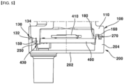
- FIG. 5 is a cross-sectional view illustrating a combined structure of a first body, a second body, and a printed circuit board according to an exemplary embodiment of the present invention
- FIG. 6 is a perspective view illustrating a portion of one of the undersides of the first body in an exemplary embodiment of the present invention
- FIG. 1 is a perspective view illustrating the appearance of a camera module according to an exemplary embodiment of the present invention
- FIG. 2 is a cross-sectional view of a camera module according to an exemplary embodiment of the present invention
- FIG. 3 is an exploded perspective view of a camera module according to
- FIG. 7 is a perspective view illustrating the coupling structure of the first body and the printed circuit board, according to an exemplary embodiment of the present invention
- FIG. 8 is a cross-sectional view of a first guide according to an exemplary embodiment of the present invention
- FIG. 9 is a cross-sectional view illustrating a combined structure of a first guide and a printed circuit board according to an exemplary embodiment of the present invention
- FIG. 10 is a perspective view of the top surface of the second body according to an exemplary embodiment of the present invention
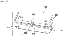
- FIG. 11 is a perspective view illustrating the coupling structure of the first body and the printed circuit board according to an exemplary embodiment of the present invention.
- the camera module (10) may be a vehicle camera module.
- the camera module (10) may be coupled to a vehicle.
- the camera module (10) may be used in one or more of a front camera, a side camera, a rear camera, and a black box of the vehicle.
- the camera module (10) may be disposed at the front of the vehicle.
- the camera module (10) may be disposed at the rear of the vehicle.
- the camera module (10) may be coupled to a windscreen of the vehicle.
- the camera module (10) may be coupled to the windscreen of the front or rear of the vehicle.
- the camera module (10) may be disposed on the side of a vehicle.
- the camera module (10) may photograph a subject and output an image to a display (not shown).
- the camera module (10) may include a first body (100).
- the first body (100) may be referred to as a front body, an upper housing, or a first housing.
- the first body (100) may include a body portion (110).
- the first body (100) may include a barrel portion (120).
- the first body (100) may include a lens (300).
- the body portion (110), barrel portion (120), and lens (300) of the first body (100) may be integrally formed. Any two or more of the body portion (110), barrel portion (120), and lens (300) of the first body (100) may be integrally formed.
- the body portion (110), the barrel portion (120), and the lens (300) may each be formed separately.
- the body portion (110) may be coupled to the barrel portion (120).
- the body portion (110) may be integrally formed with the barrel portion (120).
- the body portion (110) may be formed of a metal material.
- the body portion (110) may be disposed on the second body (200, described later).
- the body portion (110) may be coupled to the second body (200).
- a bottom end of the body portion (110) may be secured to the second body (200).
- the body portion (110) may be coupled to the second body (200) by an adhesive.
- the body portion (110) may be coupled to the printed circuit board (400, described later).
- the body portion (110) may be formed as a rectangular shape with an opening at the bottom. In this case, the corners of the body portion (110) may be rounded.
- the body portion (110) may include a top plate (112) and a first side plate (114) extending from the top plate (112).
- the top plate (112) may be formed in a rectangular shape.
- the top plate (112) may extend outwardly from a lower outer peripheral surface of the barrel portion (120).
- a first side plate (114) may extend downwardly from an outer edge of the top plate (112).
- the first side plate (114) may include a plurality of plates.
- the first side plate (114) may include four side plates.
- the first side plate (114) may be formed in the shape of a square plate.
- the first side plate (114) may include a first-1 side plate and a first-2 side plate, a first-3 side plate disposed opposite the first-1 side plate, and a first-4 side plate disposed opposite the first-2 side plate.
- the first side plate (114) may include first and fourth corners disposed among the first-1 to first-4 side plates, respectively. Each of the first to fourth corners may include a rounded shape in at least a portion.
- a space portion may be formed that is compartmentalized from other regions.
- the space portion may be open at the bottom and covered at the top by the barrel portion (120) and the lens (300).
- the body portion (110) may include a first edge region (130) (see FIGS. 5 and 9 ).
- the first edge region (130) may be disposed on an outer side of the space portion.
- the first edge region (130) may form a bottom surface of the body portion (110).
- the first edge region (130) may include a first protrusion (132), a second protrusion (180), and a first groove (134). Relative to the center of the body portion (110), the second protrusion (180) may be disposed on an inner side of the first protrusion (132), and the first groove (134) may be disposed between the first protrusion (132) and the second protrusion (180).
- the first protrusion (132) may be formed to project downwardly from a bottom surface of the body portion (110) than other areas. A lower end of the first protrusion (132) may be disposed above a top surface of the printed circuit board (300). A bottom surface of the first protrusion (132) may contact a top surface of the second side plate (204) of the second body (200), as will be described later. A lower end of the first protrusion (132) may be disposed above a lower end of the second protrusion (180).
- the second protrusion (180) may be disposed on an inner side of the first protrusion (132).
- a bottom side of the second protrusion (180) may be a bottom side of the first body (100).
- a bottom side of the second protrusion (180) may contact a top side of the printed circuit board (400). In other words, the underside of the first body (100) may contact the top surface of the printed circuit board (400).
- the bottom of the second protrusion (180) may project downwardly from the bottom of the first protrusion (132).
- a space portion may be formed on an inner side of the second protrusion (180).
- An inner surface of the second protrusion (180) may form an inner surface of the space portion.
- the first groove (134) may be disposed between the first protrusion (132) and the second protrusion (180), and may have a shape that is more upwardly recessed than other regions.
- the first groove (134) may be arranged to at least partially overlap in an optical axis direction with the second side plate (204) of the second body (200).
- An inner surface of the first groove (134) may be formed with a slope such that the cross-sectional area of the first groove (134) narrows upwardly.
- the first groove (134) may have an adhesive member (not shown) disposed therein.
- the adhesive member may include an epoxy. Upon curing of the epoxy, the first body (100) and the second body (200) may be mutually bonded. In some cases, an adhesive member may be disposed between the second protrusion (180) and the printed circuit board (400), as well as on the side of the printed circuit board (400). Areas of the outer surface of the first body (100) other than the adhesive region where the adhesive member is disposed may be coated. In other words, a metal area of the first body (100) may be exposed to the outside through the bonding area.
- the first body (100) may include a barrel portion (120).
- the barrel portion (120) may be a lens barrel.
- the barrel portion (120) may be formed of a metal material.
- the barrel portion (120) may be disposed on the body portion (110).
- the barrel portion (120) may extend from a top surface of the body portion (110).
- the barrel portion (120) may be integrally formed with the body portion (110).
- the barrel portion (120) may be coupled to the body portion (110).
- the barrel portion (120) may be secured to the body portion (110) by an adhesive.
- the barrel portion (120) may accommodate a lens (300) therein.
- the barrel portion (120) may include a hole (121).
- the lens (300) may be disposed in the hole (121) of the barrel portion (120).
- the inner circumferential surface of the hole in the barrel portion (120) may be formed in a shape and size that corresponds to the outer circumferential shape of the lens (300).
- the first body (100) may include a first guide (140).
- the first guide (140) may be formed to project downwardly from a bottom surface of the first body (100).
- the first guide (140) may project downwardly from a bottom surface of the top plate (112) and may be at least partially coupled to the printed circuit board (400).
- the first guide (140) may include a first guide body (142) projecting downwardly from a bottom surface of the top plate (112), and a first projection (150) projecting downwardly from a bottom surface of the first guide body (142).
- the first guide body (142) may have a shape that projects inwardly from an inner surface of the space within the first body (100).
- a bottom surface of the first guide body (142) may form a plane coincident with a bottom surface of the second protrusion (180).
- the first projection (150) may project downwardly from a bottom surface of the first guide body (142).
- the cross-sectional area of the first projection (150) may be formed to be smaller than the cross-sectional area of the first guide body (142).
- a lower end of the first projection (150) may be disposed lower than a lower surface of the second projection (180).
- the first protrusion (150) may be coupled to the first guide hole (430) of the printed circuit board (400), which will be described later.
- the first protrusion (150) may be soldered to the first guide hole (430).
- the first projection (150) may be circular in cross-section.
- the first projection (150) may include a first region (152) having a first diameter, and a second region (154) disposed downstream of the first region (152) and having a second diameter smaller than the first diameter.
- an inclined region (153) may be disposed to connect the first region (152) and the second region (154).
- the region between the first region (152) and the second region (154) may be disposed within the first guide hole (430), which will be described later.
- the region between the first region (152) and the second region (154) may be arranged to overlap in a direction perpendicular to the optical axis with a region comprising one-half the height of the first guide hole (430), relative to the optical axis direction.
- the outer surface of the first projection (150) may be plated.
- a plating area made of Ni, Ni+Sn may be formed on the outer surface of the first protrusion (150). Accordingly, a grounding structure may be implemented between the grounding region (450) of the printed circuit board (400, described later) and the first body (100).
- an escape groove (144) may be formed in a shape that is recessed upwardly from the other regions.
- the escape groove (144) may be disposed between the second protrusion (180) and a peripheral surface of the first protrusion (150).
- the escape groove (144) may have an arc-shaped cross-section.
- the escape groove (144) may be disposed on the outer side of the first region (152).
- the escape groove (144) allows a portion of the solder paste, such as lead, to be received so that the printed circuit board (400) and the first body (100) can be firmly bonded, and a clearance space from the top surface of the printed circuit board (400) can be provided to prevent tilting of the printed circuit board (400) with respect to the bottom surface of the second protrusion (180).
- a plurality of first guides (140) may be provided and spaced apart from each other along an edge of the first body (100).
- the first body (100) may include a second guide (162).
- the second guide (162) may be formed to project downwardly from a bottom surface of the top plate (112), and may have an upwardly recessed coupling (engagement) groove (160) disposed in its center.
- the second guide (162) may be disposed between a plurality of first guides (140) disposed adjacent to each other.
- the second guides (162) may be formed to project inwardly from an inner surface of a region forming one side of an inner surface of the space within the first body (100).
- a bottom surface of the second guide (162) may form a plane coplanar with a bottom surface of the second protrusion (180).
- the coupling groove (160) may be circular in cross-section, and allow the second body (200) to be engaged with the third guide (270).
- a slope (165) may be formed that tapers in cross-section upwardly to facilitate entry of the third guide (270) into the space within the coupling groove (160).
- the first body (100) may include a lens (300).
- the lens (300) may be disposed in the barrel portion (120).
- the lens (300) may be coupled to the barrel portion (120).
- the lens (300) may be disposed in a hole (121) of the barrel portion (120).
- the lens (300) may include a plurality of lenses (310).
- the plurality of lenses (310) may be housed in the barrel.
- the lens (300) may be aligned with an image sensor, as described later.
- the lens (300) may be optically aligned with the image sensor.
- the optical axis of the lens (300) may coincide with the optical axis of the image sensor.
- the first body (100) may include an infrared ray filter (IR filter) disposed between the lens (300) and the image sensor.
- IR filter infrared ray filter
- the outer surface of the lens (300) may be disposed with a protruding region (320) that projects outwardly.
- the protruding region (320) may be disposed on the top surface of the barrel portion (120).
- a sealing member (not shown) may be disposed between the bottom surface of the protruding region (320) and the top surface of the barrel portion (120).
- the camera module (10) may include a second body (200).
- the second body (200) may be named any one of a rear body, a lower housing, and a second housing.
- the second body (200) may be formed in a rectangular shape with an open top.
- the second body (200) may be formed of a metal material.
- the second body (200) may be disposed below the first body (100).
- the second body (200) may be coupled to the first body (100).
- the second body (200) may be coupled with the first body (100) to form an interior space.
- the second body (200) may include a space portion (207) having a top surface opening.
- the second body (200) may include a bottom plate (202).
- the bottom plate (202) may be opposite the top plate (112) of the body portion (110) of the first body (100).
- the bottom plate (202) may be spaced apart from the top plate (112) of the body portion (110) of the first body (100) in an optical axis direction.
- the bottom plate (202) may be parallel to the top plate (112) of the body portion (110) of the first body (100).
- the bottom plate (202) may be formed in a rectangular shape. In this case, the corners of the bottom plate (202) may include a rounded shape at least in part.
- the second body (200) may include a second side plate (204).
- the second side plate (204) may extend from the bottom plate (202).
- the second side plate (204) may extend from an outer edge of the bottom plate (202).
- a shield can (not shown) may be disposed on the second side plate (204).
- An inner surface of the second side plate (204) may be contacted by the shield can.
- a top of the second side plate (204) may be coupled to the first body (100).
- the top surface of the second side plate (204) may contact the underside of the first protrusion (132).
- An outer surface of the second side plate (204) may be disposed in the same plane as an outer surface of the first side plate (114) of the first body (100).
- the second body (200) may include a connector lead portion (290).
- the connector lead portion (290) may be coupled to the bottom plate (202).
- the connector lead portion (290) may be disposed in a hole (not shown) in the bottom plate (202).
- the connector lead portion (290) may pass through a hole in the bottom plate (202).
- the connector lead portion (290) may have a connector (500) disposed therein.
- the connector lead portion (290) may be formed of a metal material.
- the second body (200) may include a third guide (270).
- the third guide (270) may be formed to project upwardly from a top surface of the bottom plate (202).
- the third guide (270) may be disposed to face the second guide (162) in an optical axis direction.
- the third guide (270) may include a third guide bodies (274, 276), and a second projection (272) that projects upwardly from a top surface of the third guide bodies (274, 276) and engages the coupling groove (160).
- the cross-sectional shape of the second projection (272) may be formed to correspond to the cross-sectional shape of the coupling groove (160).
- the third guide body (274, 276) may have a plurality of regions with different cross-sectional areas.
- the third guide body (274, 276) may include a third-1 guide body (276) and a third-2 guide body (274).
- the cross-sectional area of the third-1 guide body (276) may be formed to be larger than the cross-sectional area of the third-2 guide body (274).
- the third-1 guide body (276) may be disposed at a lower portion of the third-2 guide body (274).
- the second body (200) may include a reinforcement portion (280) connecting the third guide bodies (274, 276) to the inner surface of the second side plate (204).
- An optical axis length of the reinforcement portion (280) may correspond to an optical axis length of the third guide bodies (274, 276).
- the assembly direction of the first body (100) and the second body (200) may be guided by the coupling structure of the second projection (272) and the coupling groove (160). Furthermore, the coupling structure of the second protrusion (272) and the coupling groove (160), which are disposed in a certain position, can prevent mis-assembly or mis-alignment when the printed circuit board (400) is placed.
- the camera module (10) may include a printed circuit board (400).
- the printed circuit board (400) may be disposed between the first body (100) and the second body (200).
- a top surface of the printed circuit board (400) may contact a bottom surface of the second protrusion (180).
- the printed circuit board (400) may be disposed in the space portion (207) within the second body (200).
- An image sensor (410) may be disposed on a top surface of printed circuit board (400).
- a connector (500) may be coupled to a bottom surface of the printed circuit board (400).
- the printed circuit board (400) may be electrically connected to the connector (500).
- a first guide hole (430) may be disposed in a region of the printed circuit board (400) that faces the first guide (140).
- the first guide hole (430) may be formed to extend downwardly from a top surface of the printed circuit board (400).
- the first guide hole (430) may be provided in a plurality, corresponding to a number and location of the first guide (140). In one example, the first guide hole (430) may be disposed in each corner region of the printed circuit board (400).
- the first protrusion (150) may be coupled to the first guide hole (430).
- the first projection (150) may be soldered to the first guide hole (430).
- a solder portion (250) may be disposed in the forming region of the first guide hole (430) on the top and bottom of the printed circuit board (400).
- a grounding region (450) of the ground power source may be formed on the outer side of the first guide hole (430) among the upper and lower sides of the printed circuit board (400). Accordingly, a grounding structure of the first body (100) and the printed circuit board (400) may be implemented.
- a second guide hole (420) may be disposed in a region of the printed circuit board (400) that faces the second guide (162) or the third guide (270).
- the second guide hole (420) may be disposed in a region of the printed circuit board (400) that faces the second guide (162) or the third guide (270.
- the second guide hole (420) may be formed to extend downwardly from the top surface of the printed circuit board (400). When viewed from the side, the second guide hole (420) may have a recessed shape that is more inwardly recessed than other areas.
- the second guide hole (420) may have a second projection (272) engaged to penetrate it.
- the second guide hole (420) may engage a lower portion of the second guide (162).
- the coupling direction of the second body (200) may be guided primarily by the coupling structure between the connector (500) and the connector lead portion (290), and the coupling structure of the second guide hole (420), the coupling groove (160), and the second protrusion (272) may provide secondary guidance of the coupling of the second body (200).
- the first body, the second body, and the printed circuit board are electrically connected to form a ground region, so that electromagnetic waves generated in the circuit region of the printed circuit board can be prevented from radiating outward and affecting adjacent electronic components or from entering the printed circuit board, thereby further improving the electrical characteristics of the camera module and preventing the inclusion of noise in the electrical signals, resulting in an image of excellent quality.
- the printed circuit board and the first body are joined by soldering to thereby provide the advantage of reducing the manufacturing cost by reducing the number of components.
Landscapes
- Engineering & Computer Science (AREA)
- Multimedia (AREA)
- Signal Processing (AREA)
- Microelectronics & Electronic Packaging (AREA)
- Studio Devices (AREA)
- Camera Bodies And Camera Details Or Accessories (AREA)
- Credit Cards Or The Like (AREA)
- Transforming Light Signals Into Electric Signals (AREA)
- Mounting Of Printed Circuit Boards And The Like (AREA)
Applications Claiming Priority (2)
| Application Number | Priority Date | Filing Date | Title |
|---|---|---|---|
| KR1020210087298A KR20230006278A (ko) | 2021-07-02 | 2021-07-02 | 카메라 모듈 |
| PCT/KR2022/009561 WO2023277668A1 (ko) | 2021-07-02 | 2022-07-01 | 카메라 모듈 |
Publications (2)
| Publication Number | Publication Date |
|---|---|
| EP4366318A1 true EP4366318A1 (de) | 2024-05-08 |
| EP4366318A4 EP4366318A4 (de) | 2025-05-28 |
Family
ID=84691995
Family Applications (1)
| Application Number | Title | Priority Date | Filing Date |
|---|---|---|---|
| EP22833721.8A Pending EP4366318A4 (de) | 2021-07-02 | 2022-07-01 | Kameramodul |
Country Status (6)
| Country | Link |
|---|---|
| US (1) | US20240314922A1 (de) |
| EP (1) | EP4366318A4 (de) |
| JP (1) | JP2024529293A (de) |
| KR (1) | KR20230006278A (de) |
| CN (1) | CN117616766A (de) |
| WO (1) | WO2023277668A1 (de) |
Families Citing this family (2)
| Publication number | Priority date | Publication date | Assignee | Title |
|---|---|---|---|---|
| KR20250082891A (ko) * | 2023-11-30 | 2025-06-09 | 엘지이노텍 주식회사 | 카메라 모듈 |
| KR20250165116A (ko) * | 2024-05-17 | 2025-11-25 | 엘지이노텍 주식회사 | 카메라 모듈 |
Family Cites Families (15)
| Publication number | Priority date | Publication date | Assignee | Title |
|---|---|---|---|---|
| JP3241019B2 (ja) * | 1999-03-15 | 2001-12-25 | 日本電気株式会社 | コプレーナ線路 |
| EP2136552A1 (de) * | 2007-04-13 | 2009-12-23 | Panasonic Corporation | Festkörperabbildungsvorrichtung und verfahren zu ihrer herstellung |
| KR101022870B1 (ko) * | 2009-11-10 | 2011-03-16 | 삼성전기주식회사 | 카메라 모듈 |
| KR101376882B1 (ko) * | 2012-11-15 | 2014-03-20 | 삼성전기주식회사 | 차량용 카메라 |
| KR101952853B1 (ko) * | 2013-07-12 | 2019-02-27 | 삼성전기주식회사 | 카메라 모듈 |
| KR102279786B1 (ko) * | 2015-02-26 | 2021-07-21 | 엘지이노텍 주식회사 | 카메라 모듈 및 차량용 카메라 |
| KR102374766B1 (ko) * | 2015-09-01 | 2022-03-16 | 엘지이노텍 주식회사 | 카메라 모듈, 차량용 카메라 및 카메라 모듈의 제조방법 |
| KR102502284B1 (ko) * | 2016-01-12 | 2023-02-22 | 엘지이노텍 주식회사 | 카메라 모듈 |
| WO2018066911A1 (ko) * | 2016-10-06 | 2018-04-12 | 엘지이노텍 주식회사 | 카메라 모듈 및 카메라 모듈 제조 방법 |
| JP2018098660A (ja) * | 2016-12-13 | 2018-06-21 | 日本電産コパル株式会社 | 撮像装置 |
| KR102323625B1 (ko) * | 2017-04-21 | 2021-11-08 | 엘지이노텍 주식회사 | 카메라 모듈 및 자동차 |
| KR102371643B1 (ko) * | 2017-07-04 | 2022-03-08 | 엘지이노텍 주식회사 | 카메라 모듈 |
| KR102433450B1 (ko) * | 2017-11-29 | 2022-08-17 | 엘지이노텍 주식회사 | 카메라 모듈 |
| US20190373142A1 (en) * | 2018-05-31 | 2019-12-05 | Sharp Kabushiki Kaisha | Imaging apparatus |
| KR102902591B1 (ko) * | 2019-11-12 | 2025-12-22 | 엘지이노텍 주식회사 | 카메라 모듈 |
-
2021
- 2021-07-02 KR KR1020210087298A patent/KR20230006278A/ko active Pending
-
2022
- 2022-07-01 CN CN202280047281.9A patent/CN117616766A/zh active Pending
- 2022-07-01 JP JP2024500084A patent/JP2024529293A/ja active Pending
- 2022-07-01 US US18/575,572 patent/US20240314922A1/en active Pending
- 2022-07-01 EP EP22833721.8A patent/EP4366318A4/de active Pending
- 2022-07-01 WO PCT/KR2022/009561 patent/WO2023277668A1/ko not_active Ceased
Also Published As
| Publication number | Publication date |
|---|---|
| WO2023277668A1 (ko) | 2023-01-05 |
| JP2024529293A (ja) | 2024-08-06 |
| EP4366318A4 (de) | 2025-05-28 |
| US20240314922A1 (en) | 2024-09-19 |
| CN117616766A (zh) | 2024-02-27 |
| KR20230006278A (ko) | 2023-01-10 |
Similar Documents
| Publication | Publication Date | Title |
|---|---|---|
| US20250334859A1 (en) | Camera module | |
| EP4366318A1 (de) | Kameramodul | |
| US20240380963A1 (en) | Camera module | |
| US20240361675A1 (en) | Camera module | |
| EP4369093A1 (de) | Kameramodul | |
| US20250365487A1 (en) | Camera module | |
| JP2023532030A (ja) | カメラモジュール | |
| US20240348901A1 (en) | Camera module | |
| US20240284022A1 (en) | Camera module | |
| US12487507B2 (en) | Camera module | |
| KR20250123011A (ko) | 카메라 모듈 | |
| US20260025563A1 (en) | Camera module | |
| CN220603691U (zh) | 雷达视频一体机 | |
| KR20250019994A (ko) | 카메라 모듈 | |
| KR20250129424A (ko) | 카메라 모듈 | |
| KR20250062332A (ko) | 카메라 모듈 | |
| KR20250082891A (ko) | 카메라 모듈 | |
| KR20250062331A (ko) | 카메라 모듈 |
Legal Events
| Date | Code | Title | Description |
|---|---|---|---|
| STAA | Information on the status of an ep patent application or granted ep patent |
Free format text: STATUS: THE INTERNATIONAL PUBLICATION HAS BEEN MADE |
|
| PUAI | Public reference made under article 153(3) epc to a published international application that has entered the european phase |
Free format text: ORIGINAL CODE: 0009012 |
|
| STAA | Information on the status of an ep patent application or granted ep patent |
Free format text: STATUS: REQUEST FOR EXAMINATION WAS MADE |
|
| 17P | Request for examination filed |
Effective date: 20240102 |
|
| AK | Designated contracting states |
Kind code of ref document: A1 Designated state(s): AL AT BE BG CH CY CZ DE DK EE ES FI FR GB GR HR HU IE IS IT LI LT LU LV MC MK MT NL NO PL PT RO RS SE SI SK SM TR |
|
| DAV | Request for validation of the european patent (deleted) | ||
| DAX | Request for extension of the european patent (deleted) | ||
| REG | Reference to a national code |
Ref country code: DE Ref legal event code: R079 Free format text: PREVIOUS MAIN CLASS: H04N0023000000 Ipc: H04N0023510000 |
|
| A4 | Supplementary search report drawn up and despatched |
Effective date: 20250428 |
|
| RIC1 | Information provided on ipc code assigned before grant |
Ipc: H04N 23/51 20230101AFI20250422BHEP |