EP4341995B1 - Leistungselektronische baugruppe - Google Patents
Leistungselektronische baugruppe Download PDFInfo
- Publication number
- EP4341995B1 EP4341995B1 EP22751342.1A EP22751342A EP4341995B1 EP 4341995 B1 EP4341995 B1 EP 4341995B1 EP 22751342 A EP22751342 A EP 22751342A EP 4341995 B1 EP4341995 B1 EP 4341995B1
- Authority
- EP
- European Patent Office
- Prior art keywords
- structures
- insulator
- electronics assembly
- power electronics
- power
- Prior art date
- Legal status (The legal status is an assumption and is not a legal conclusion. Google has not performed a legal analysis and makes no representation as to the accuracy of the status listed.)
- Active
Links
Images

Classifications
-
- H—ELECTRICITY
- H10—SEMICONDUCTOR DEVICES; ELECTRIC SOLID-STATE DEVICES NOT OTHERWISE PROVIDED FOR
- H10W—GENERIC PACKAGES, INTERCONNECTIONS, CONNECTORS OR OTHER CONSTRUCTIONAL DETAILS OF DEVICES COVERED BY CLASS H10
- H10W40/00—Arrangements for thermal protection or thermal control
- H10W40/20—Arrangements for cooling
- H10W40/25—Arrangements for cooling characterised by their materials
- H10W40/255—Arrangements for cooling characterised by their materials having a laminate or multilayered structure, e.g. direct bond copper [DBC] ceramic substrates
-
- H—ELECTRICITY
- H10—SEMICONDUCTOR DEVICES; ELECTRIC SOLID-STATE DEVICES NOT OTHERWISE PROVIDED FOR
- H10W—GENERIC PACKAGES, INTERCONNECTIONS, CONNECTORS OR OTHER CONSTRUCTIONAL DETAILS OF DEVICES COVERED BY CLASS H10
- H10W70/00—Package substrates; Interposers; Redistribution layers [RDL]
- H10W70/40—Leadframes
- H10W70/421—Shapes or dispositions
- H10W70/435—Shapes or dispositions of insulating layers on leadframes, e.g. bridging members
-
- H—ELECTRICITY
- H05—ELECTRIC TECHNIQUES NOT OTHERWISE PROVIDED FOR
- H05K—PRINTED CIRCUITS; CASINGS OR CONSTRUCTIONAL DETAILS OF ELECTRIC APPARATUS; MANUFACTURE OF ASSEMBLAGES OF ELECTRICAL COMPONENTS
- H05K1/00—Printed circuits
- H05K1/02—Details
- H05K1/0201—Thermal arrangements, e.g. for cooling, heating or preventing overheating
- H05K1/0203—Cooling of mounted components
- H05K1/0209—External configuration of printed circuit board adapted for heat dissipation, e.g. lay-out of conductors, coatings
-
- H—ELECTRICITY
- H05—ELECTRIC TECHNIQUES NOT OTHERWISE PROVIDED FOR
- H05K—PRINTED CIRCUITS; CASINGS OR CONSTRUCTIONAL DETAILS OF ELECTRIC APPARATUS; MANUFACTURE OF ASSEMBLAGES OF ELECTRICAL COMPONENTS
- H05K1/00—Printed circuits
- H05K1/02—Details
- H05K1/03—Use of materials for the substrate
- H05K1/0306—Inorganic insulating substrates, e.g. ceramic, glass
-
- H—ELECTRICITY
- H10—SEMICONDUCTOR DEVICES; ELECTRIC SOLID-STATE DEVICES NOT OTHERWISE PROVIDED FOR
- H10W—GENERIC PACKAGES, INTERCONNECTIONS, CONNECTORS OR OTHER CONSTRUCTIONAL DETAILS OF DEVICES COVERED BY CLASS H10
- H10W40/00—Arrangements for thermal protection or thermal control
- H10W40/20—Arrangements for cooling
- H10W40/25—Arrangements for cooling characterised by their materials
- H10W40/254—Diamond
-
- H—ELECTRICITY
- H10—SEMICONDUCTOR DEVICES; ELECTRIC SOLID-STATE DEVICES NOT OTHERWISE PROVIDED FOR
- H10W—GENERIC PACKAGES, INTERCONNECTIONS, CONNECTORS OR OTHER CONSTRUCTIONAL DETAILS OF DEVICES COVERED BY CLASS H10
- H10W42/00—Arrangements for protection of devices
- H10W42/80—Arrangements for protection of devices protecting against overcurrent or overload, e.g. fuses or shunts
-
- H—ELECTRICITY
- H10—SEMICONDUCTOR DEVICES; ELECTRIC SOLID-STATE DEVICES NOT OTHERWISE PROVIDED FOR
- H10W—GENERIC PACKAGES, INTERCONNECTIONS, CONNECTORS OR OTHER CONSTRUCTIONAL DETAILS OF DEVICES COVERED BY CLASS H10
- H10W90/00—Package configurations
-
- H—ELECTRICITY
- H05—ELECTRIC TECHNIQUES NOT OTHERWISE PROVIDED FOR
- H05K—PRINTED CIRCUITS; CASINGS OR CONSTRUCTIONAL DETAILS OF ELECTRIC APPARATUS; MANUFACTURE OF ASSEMBLAGES OF ELECTRICAL COMPONENTS
- H05K2201/00—Indexing scheme relating to printed circuits covered by H05K1/00
- H05K2201/10—Details of components or other objects attached to or integrated in a printed circuit board
- H05K2201/10007—Types of components
- H05K2201/10166—Transistor
-
- H—ELECTRICITY
- H10—SEMICONDUCTOR DEVICES; ELECTRIC SOLID-STATE DEVICES NOT OTHERWISE PROVIDED FOR
- H10W—GENERIC PACKAGES, INTERCONNECTIONS, CONNECTORS OR OTHER CONSTRUCTIONAL DETAILS OF DEVICES COVERED BY CLASS H10
- H10W72/00—Interconnections or connectors in packages
- H10W72/071—Connecting or disconnecting
- H10W72/075—Connecting or disconnecting of bond wires
- H10W72/07541—Controlling the environment, e.g. atmosphere composition or temperature
- H10W72/07554—Controlling the environment, e.g. atmosphere composition or temperature changes in dispositions
-
- H—ELECTRICITY
- H10—SEMICONDUCTOR DEVICES; ELECTRIC SOLID-STATE DEVICES NOT OTHERWISE PROVIDED FOR
- H10W—GENERIC PACKAGES, INTERCONNECTIONS, CONNECTORS OR OTHER CONSTRUCTIONAL DETAILS OF DEVICES COVERED BY CLASS H10
- H10W72/00—Interconnections or connectors in packages
- H10W72/50—Bond wires
- H10W72/541—Dispositions of bond wires
- H10W72/5445—Dispositions of bond wires being orthogonal to a side surface of the chip, e.g. parallel arrangements
-
- H—ELECTRICITY
- H10—SEMICONDUCTOR DEVICES; ELECTRIC SOLID-STATE DEVICES NOT OTHERWISE PROVIDED FOR
- H10W—GENERIC PACKAGES, INTERCONNECTIONS, CONNECTORS OR OTHER CONSTRUCTIONAL DETAILS OF DEVICES COVERED BY CLASS H10
- H10W72/00—Interconnections or connectors in packages
- H10W72/50—Bond wires
- H10W72/541—Dispositions of bond wires
- H10W72/547—Dispositions of multiple bond wires
- H10W72/5475—Dispositions of multiple bond wires multiple bond wires connected to common bond pads at both ends of the wires
-
- H—ELECTRICITY
- H10—SEMICONDUCTOR DEVICES; ELECTRIC SOLID-STATE DEVICES NOT OTHERWISE PROVIDED FOR
- H10W—GENERIC PACKAGES, INTERCONNECTIONS, CONNECTORS OR OTHER CONSTRUCTIONAL DETAILS OF DEVICES COVERED BY CLASS H10
- H10W72/00—Interconnections or connectors in packages
- H10W72/90—Bond pads, in general
- H10W72/921—Structures or relative sizes of bond pads
- H10W72/926—Multiple bond pads having different sizes
-
- H—ELECTRICITY
- H10—SEMICONDUCTOR DEVICES; ELECTRIC SOLID-STATE DEVICES NOT OTHERWISE PROVIDED FOR
- H10W—GENERIC PACKAGES, INTERCONNECTIONS, CONNECTORS OR OTHER CONSTRUCTIONAL DETAILS OF DEVICES COVERED BY CLASS H10
- H10W90/00—Package configurations
- H10W90/701—Package configurations characterised by the relative positions of pads or connectors relative to package parts
- H10W90/751—Package configurations characterised by the relative positions of pads or connectors relative to package parts of bond wires
- H10W90/753—Package configurations characterised by the relative positions of pads or connectors relative to package parts of bond wires between laterally-adjacent chips
-
- H—ELECTRICITY
- H10—SEMICONDUCTOR DEVICES; ELECTRIC SOLID-STATE DEVICES NOT OTHERWISE PROVIDED FOR
- H10W—GENERIC PACKAGES, INTERCONNECTIONS, CONNECTORS OR OTHER CONSTRUCTIONAL DETAILS OF DEVICES COVERED BY CLASS H10
- H10W90/00—Package configurations
- H10W90/701—Package configurations characterised by the relative positions of pads or connectors relative to package parts
- H10W90/751—Package configurations characterised by the relative positions of pads or connectors relative to package parts of bond wires
- H10W90/754—Package configurations characterised by the relative positions of pads or connectors relative to package parts of bond wires between a chip and a stacked insulating package substrate, interposer or RDL
-
- H—ELECTRICITY
- H10—SEMICONDUCTOR DEVICES; ELECTRIC SOLID-STATE DEVICES NOT OTHERWISE PROVIDED FOR
- H10W—GENERIC PACKAGES, INTERCONNECTIONS, CONNECTORS OR OTHER CONSTRUCTIONAL DETAILS OF DEVICES COVERED BY CLASS H10
- H10W90/00—Package configurations
- H10W90/701—Package configurations characterised by the relative positions of pads or connectors relative to package parts
- H10W90/751—Package configurations characterised by the relative positions of pads or connectors relative to package parts of bond wires
- H10W90/756—Package configurations characterised by the relative positions of pads or connectors relative to package parts of bond wires between a chip and a stacked lead frame, conducting package substrate or heat sink
Definitions
- the invention relates to a power electronic assembly.
- the invention further relates to methods for producing a semi-finished product for the power electronic assembly.
- Such a power electronic assembly is used, for example, in power modules for converters.
- Applications can include electrical drive technology, voltage conversion, or energy technology.
- the switching components In today's circuit boards for power electronic assemblies, the switching components (IGBTs, MOSFETs, etc.) are located on metallic conductors, which, on the one hand, conduct current and, on the other hand, spread the semiconductor's waste heat and direct it to a cooler.
- Circuits usually exhibit large temperature differences during operation, i.e., hot regions or structures close to the semiconductor chip and cooler regions or structures that are usually further away from the chip or thermally separated (e.g., gate contacts, emitter sense, shunt contacts, etc.). These temperature differences mean that base plates are now used for temperature distribution, or the cooler itself requires a more complex design.
- DE 10 2010 024520 A1 discloses a method for increasing the thermo-mechanical resistance of a metal-ceramic substrate having a metallization with a thickness of ⁇ 100 ⁇ m on a substrate or a layer of a ceramic material.
- the invention is based on the object of providing an improved power electronic assembly.
- the power electronic assembly comprises a substrate with a metallization.
- the metallization is structured.
- the metallization has spaces for structuring through which separate first and second structures are formed.
- the metallization has a thickness of at least 300 ⁇ m. In further preferred embodiments, the metallization has a thickness of at least 0.5 or 1 mm, 2 mm, 3 mm or 4 mm.
- the first metallic structures have a power semiconductor.
- the power semiconductor is generally joined to the first structures, e.g. soldered or sintered.
- the first structures are thus provided with a heat-generating component and have a higher heat load than the second structures, which preferably do not have a power semiconductor.
- switching and non-switching components such as IGBTs, MOSFETs, diodes or other semiconductor switches with a wide band gap can be considered as power semiconductors.
- an electrical insulator is arranged at least in sections with respect to the gaps such that the structures adjacent to the gap are thermally connected by the insulator.
- the insulator has a thermal conductivity of at least 50 W/mK.
- the insulator has a thermal conductivity of at least 100 W/mK, 200 W/mK, or 500 W/mK.
- Such a substrate with metallization can, for example, be designed as a thick copper substrate.
- a thick copper substrate also organic DBC
- ODBC Organic direct copper bond
- the plastic can compensate for significantly higher thermo-mechanical forces (e.g., due to a CTE mismatch) and thus allow for the implementation of correspondingly thicker metal layers.
- DBC ceramic substrates
- AMB where the large metallization or copper thicknesses can lead to faster failure (e.g., conchoidal fracture of the ceramic)
- plastic has proven to be a suitable substrate material.
- the thermal conductivity refers to the thermal conductivity of the insulator at an ambient temperature of 20°C.
- the metallization is at most 7 mm thick, in particular at most 4 mm thick.
- the gaps have a width of at least 0.1 mm and at most 8 mm.
- the gaps have a width of between 0.3 and 5 mm.
- the insulator covers 50% of the height of the recesses.
- the height of the recesses corresponds to the height of the metallization.
- the insulator can fill 80%-100% of the height of the recess. It is also possible for the insulator to protrude slightly from the recess. Considering the recesses in the plane of the metallization, the insulator can preferably cover 50% of the recess between the two structures to be thermally bonded to enable the best possible heat transfer.
- the second structures do not have any power semiconductors.
- Such second structures are often designed to contact the power terminals and are electrically connected, for example, via bond wires, to the top surfaces of the power semiconductors used. From a thermal perspective, the second structures are subject to low load and therefore have a significant heat dissipation potential. Thus, it is advantageous possible to include the second structures in the cooling of the entire power electronic assembly.
- At least one of the first structures is thermally connected to at least one of the second structures by the insulator.
- those structures that have different thermal loads are connected to one another.
- the hotter or warmer first structures, which contain the power semiconductors are connected to the second structures, which in turn do not contain any power semiconductors. This makes the temperature distribution on the power electronic assembly more uniform, improving heat dissipation and allowing for better utilization of the available heat sink surface.
- the power electronic assembly comprises a shunt that is electrically contacted with one of the first structures and one of the second structures, which are thermally connected to one another by one of the insulators.
- the insulator comprises diamond.
- Diamonds are available as artificially produced industrial diamonds on an industrial scale and can now also be produced in larger layers (CVD, PVD, etc.). Diamond has an extremely high thermal conductivity of up to 2,000 W/mK with very good electrical insulation properties and is therefore very well suited as an insulator in this case.
- Metallized diamond platelets can be used. It is also conceivable, for example, to provide a diamond powder-filled insulator or even ceramic insulators (e.g., Si3N4, AlN, etc.) for less demanding requirements.
- the insulator is made of diamond.
- a diamond insulator which enables even heat distribution across the electrical assembly, is particularly advantageous for applications with a high power profile and high power density.
- the insulator is arranged in the gap and/or in the substrate in such a way that the insulator is in direct contact with the thermally connected structures. It is conceivable that this is done on one side only with one of the structures or on both sides with both structures. Direct contact has the advantage that no additional material needs to be introduced.
- the insulator is thermally connected to the adjacent structures via a thermally conductive polymer and/or resin.
- a thermally conductive polymer and/or resin can be formed, for example, as polyimide or filled epoxy materials.
- Suitable filler particles here include, for example, ceramic particles such as aluminum nitride, boron nitride, Si3N4, and/or Al2O3.
- the connection between the insulator and the structures can be electrically non-insulating (i.e., at least partially electrically conductive), since the insulation is already provided by the insulator.
- Metallic and graphite-based fillers are also conceivable.
- connection of the insulator via a very thin layer of thermally conductive polymer and/or resin has the great advantage that, especially when the thermal load on the assembly is changing, the thermal contact between the insulator and the adjacent structures better withstands the stresses resulting from CTE differences. Especially with regard to the thermal deformation of the assembly, This is advantageous.
- the insulator can also be connected to the adjacent structures via a metallic bond (e.g., a solder layer or a sintered layer).
- the insulator has an electrically insulated metallization at its ends, e.g., two separate metallized surfaces. Furthermore, the insulator's metallization is joined to the structures on the top side. Soldering or sintering are particularly suitable here.
- the power electronic assembly is designed as a half-bridge.
- the half-bridge has at least two power semiconductors designed as semiconductor switches.
- the power semiconductors are each arranged on a first structure, wherein the first structures on which the power semiconductor switches are arranged are each thermally connected to a second structure via an insulator.
- one of the semiconductor switches is the high side and one of the semiconductor switches is the low side of the half-bridge. Both (high and low sides) are thermally connected to the less stressed second structures, which results in the resulting waste heat being distributed more evenly across the entire assembly. The more even distribution of heat across the assembly can mean that the module or assembly can provide higher power or that smaller semiconductor switches can be used while maintaining the same power.
- the half-bridge can of course be expanded to a full bridge or a three-phase configuration.
- the object is further achieved by a method for producing a semi-finished product for the assembly according to the invention.
- Semi-finished products for the substrate, the structures, and the insulators are provided.
- Such semi-finished products can be, for example, copper foils and plastic prepregs.
- the insulators can be, for example, diamond platelets.
- the semi-finished products are then stacked on top of each other, for example, and the insulators are already positioned in the spaces that form the gaps. In the next step, the semi-finished products can be pressed together, bonding them together and creating thermal contact between the resulting structures and the insulators.
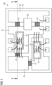
- Figure 1 shows a power electronic assembly 100 with a substrate 20 on which a metallization 30 is applied.
- the metallization 30 has first structures 35 and second structures 36.
- the power electronic assembly 100 is designed in the present case as a power electronic circuit in the form of a half-bridge with IGBTs, diodes, and a shunt.
- the first structures 35 have power semiconductors 50. These power semiconductors 50 generate waste heat, which must be conducted away from the first structures 35.
- a thermal connection is provided to the second structures 36, which is designed by an electrical insulator 42 with high thermal conductivity.
- the highly thermally conductive insulators 42 are arranged in spaces 40 between the first and second structures 35, 36 in such a way that thermal contact between the warm first structures 35 and the cooler second structures 36. Considered across the entire power electronic assembly 100, this results in significantly improved heat dissipation, which significantly simplifies heat dissipation.
- the power semiconductors are contacted with bonding wires 52 in this case, but can also be connected with other contacting means.
- the power electronic assembly comprises a shunt 60.
- the shunt 60 is arranged such that it connects a first structure 35 to one of the second structures 36 for current measurement. Since the most uniform temperature distribution possible between the two contacts of the shunt 60 is necessary for current measurement, it is particularly advantageous if the shunt 60 is arranged on the first structures 35 and the second structures 36 such that they are each connected to a highly thermally conductive insulator 42. This significantly reduces the temperature difference between the warm first structures 35 and the second structures 36.
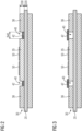
- FIG. 2 shows a section through the Figure 1 shown power electronic assembly 100.
- the substrate insulation 20 has a thickness D20 of approximately 20 ⁇ m-1000 ⁇ m.
- the metallization 30 has a thickness D30 of approximately 300 ⁇ m to 4 mm.
- the gaps 40 have a width B40 of approximately 200 ⁇ m to 5 mm.
- the insulators 42 according to the invention are arranged in the gaps 40 such that the first structure 35 arranged in the center, which in turn has two power semiconductors 50, is thermally connected via the insulators 42 to the second structures 36 arranged at the edge. This leads to a significantly more uniform heat distribution in the power electronics assembly.
- Figure 3 shows the cross section as it is in Figure 2 is shown, wherein the insulators 42 are not arranged in the gaps 40, but span them like a bridge.
- This arrangement can be realized, for example, with metallized insulators 42 (the metallization is located at both ends here), which is soldered onto the metallization 30. This also results in significantly improved thermal spread.
- Figure 4 schematically shows one possibility for stacking an insulator 42 during production.
- the insulator 42 is surrounded by an insulating material 44, for example, a polyimide or a filled epoxy material, and does not directly touch the first structures 35, 36 of the metallization 30.
- an insulating material 44 for example, a polyimide or a filled epoxy material.
- Figure 5 shows an alternative to the Figure 4 shown stack structure.
- the structures 35, 36 are in direct contact with the insulator 42. During pressing, good thermal contact is also achieved between the structures 35, 36 and the insulator 42.
- the invention relates to a power electronic assembly 100 and a method for producing a semi-finished product for a power electronic assembly 100.
- a substrate insulation 20 with a metallization 30, which forms first and second structures 35, 36 separated from one another by gaps 40 and has a thickness D30 of at least 300 ⁇ m, wherein a power semiconductor 50 is applied to the first structures 35.
- an electrical insulator 42 with a thermal conductivity of at least 50 W/mK is arranged at least in sections such that the structures 35, 36 adjacent to the respective gap 40 are thermally connected by the insulator 42.
Landscapes
- Engineering & Computer Science (AREA)
- Microelectronics & Electronic Packaging (AREA)
- Chemical & Material Sciences (AREA)
- Ceramic Engineering (AREA)
- Inorganic Chemistry (AREA)
- Cooling Or The Like Of Semiconductors Or Solid State Devices (AREA)
Description
- Die Erfindung betrifft eine leistungselektronische Baugruppe.
- Die Erfindung betrifft weiterhin Verfahren zum Herstellen eines Halbzeugs für die leistungselektronischen Baugruppe.
- Eine derartige leistungselektronische Baugruppe kommt beispielsweise in Leistungsmodulen für Umrichter zum Einsatz. Anwendungen können hierbei im Bereich der elektrischen Antriebstechnik, der Spannungswandlung oder der Energietechnik liegen.
- Bei heutigen Schaltungsträgern für leistungselektronische Baugruppen befinden sich die schaltenden Bauelemente (IGBTs, MOSFETS, ...) auf metallischen Leiterbahnen, welche einerseits die Aufgabe haben, den Strom zu leiten, aber auch die Abwärme des Halbleiters aufzuspreizen und zu einem Kühler zu leiten. Je dicker die Kupferlagen, desto effizienter findet dabei die laterale Wärmeverteilung statt. Schaltungen weisen im Betrieb meist hohe Temperaturunterschiede auf, d.h. heiße Regionen bzw. Strukturen nahe dem Halbleiterchip und kühlere Regionen bzw. Strukturen, welche vom Chip meist weiter entfernt sind bzw. thermisch getrennt sind (z.B. Gatekontakte, Emittersense, Shuntkontakte, ...). Diese Temperaturunterschiede führen dazu, dass heute Bodenplatten zur Temperaturverteilung eingesetzt werden oder auch der Kühler selbst aufwendiger gestaltet werden muss.
-
DE 10 2010 024520 A1 offenbart ein Verfahren zur Erhöhung der thermo-mechanischen Beständigkeit eines Metall-Keramik-Substrats, das eine Metallisierung mit einer Dicke von ≥ 100 µm auf einem Substrat oder einer Schicht aus einem keramischen Material aufweist. - Der Erfindung liegt die Aufgabe zugrunde, eine verbesserte leistungselektronische Baugruppe anzugeben.
- Diese Aufgabe wird durch eine leistungselektronische Baugruppe mit den im Anspruch 1 angegebenen Merkmalen gelöst. Die leistungselektronische Baugruppe umfasst dabei ein Substrat mit einer Metallisierung. Die Metallisierung ist strukturiert ausgeführt. Die Metallisierung weist zur Strukturierung Zwischenräume auf, durch die sich voneinander getrennte erste und zweite Strukturen ausbilden. Die Metallisierung weist dabei eine Dicke von zumindest 300 µm auf. In weiteren bevorzugten Ausführungsformen weist die Metallisierung eine Dicke von zumindest 0,5 bzw. 1 mm, 2mm, 3mm oder 4mm auf. Die ersten metallischen Strukturen weisen dabei einen Leistungshalbleiter auf. Der Leistungshalbleiter ist in aller Regel auf die ersten Strukturen gefügt, z.B. gelötet oder gesintert. Die ersten Strukturen sind somit mit einem wärmeerzeugenden Bauteil versehen und weisen eine höhere Wärmebelastung auf als die zweiten Strukturen, die vorzugsweise keinen Leistungshalbleiter aufweisen. Als Leistungshalbleiter kommen im vorliegenden Fall schaltende und nichtschaltende Bauelemente wie beispielsweise IGBTs, MOSFETs, Dioden oder andere Halbleiterschalter mit großem Bandabstand infrage.
- Weiterhin ist erfindungsgemäß bezüglich der Zwischenräume zumindest abschnittsweise ein elektrischer Isolator so angeordnet, dass die jeweils an den Zwischenraum angrenzenden Strukturen durch den Isolator thermisch verbunden sind. Der Isolator weist dabei eine Wärmeleitfähigkeit von zumindest 50 W/mK auf. Insbesondere weist der Isolator eine Wärmeleitfähigkeit von zumindest 100 W/mK, 200 W/mK oder 500 W/mK auf. Derartig hohe Wärmeleitfähigkeiten sorgen dafür, dass trotz vergleichsweise geringer Flächen eine hohe Wärmeabfuhr aus den ersten Strukturen ermöglicht wird. Das Ergebnis ist eine gleichmäßigere Verteilung der Wärme über die gesamte leistungselektronische Baugruppe. Als Werkstoffe können hier wärmeleitende Diamantwerkstoffe und bestimmte Keramiken (Si3N4 und AlN) verwendet werden.
- Ein solches Substrat mit einer Metallisierung kann beispielsweise als ein Dickkupfersubstrat ausgebildet sein. Unter einem Dickkupfersubstrat (auch organisches DBC) ist ein Schaltungsträger zu verstehen, der ein Metall (Cu, Al, ...) mit einer Dicke von > 300 µm aufweist (üblicherweise 1 - 4 mm) und dessen Isolationsmaterial insbesondere aus einem Kunststoff oder Kunststoffverbundmaterial besteht. Ein Beispiel ist das organic direct copper bond (ODBC). Durch den Kunststoff können deutlich höhere thermo-mechanische Kräfte (z. B. durch einen CTE Mismatch) ausgeglichen werden und dementsprechend hohe Metallschichtdicken umgesetzt werden. Im Vergleich zu keramischen Substraten (DBC, AMB), wo die großen Metallisierungs- bzw. Kupferdicken zu einem schnelleren Versagen führen können (z. B. Muschelbruch der Keramik), hat sich Kunststoff als Substratmaterial bewährt.
- Die Wärmeleitfähigkeit bezieht sich dabei, wenn nicht anders angegeben, auf die Wärmeleitfähigkeit des Isolators bei 20°C Umgebungstemperatur.
- In einer weiteren Ausführungsform ist die Metallisierung höchstens 7 mm, insbesondere höchstens 4 mm dick. Weiterhin weisen die Zwischenräume eine Breite von zumindest 0,1 mm auf und höchstens 8 mm auf. Vorzugsweise weisen die Zwischenräume eine Breite von 0,3 und 5 mm auf.
- In einer weiteren Ausführungsform ist der Isolator 50% der Höhe der Aussparungen auf. Die Höhe der Aussparungen entspricht der Höhe der Metallisierung. In weiteren Ausführungsformen kann der Isolator 80% -100% der Höhe der Aussparung ausfüllen. Es ist ebenso möglich, dass der Isolator aus der Aussparung etwas heraussteht. Betrachtet man die Aussparungen in der Ebene der Metallisierung, so kann der Isolator hier um einen möglichst guten Wärmeübergang zu ermöglichen vorzugsweise 50% der zwischen den beiden thermisch zu verbindenden Strukturen liegenden Aussparung abdecken.
- In einer besonders bevorzugten Ausführungsform weisen die zweiten Strukturen keine Leistungshalbleiter auf. Derartige zweite Strukturen sind oftmals zur Kontaktierung der Leistungsanschlüsse ausgebildet und sind elektrisch zum Beispiel über Bond-Drähte mit den Oberseiten der verwendeten Leistungshalbleiter kontaktiert. Aus thermischer Sicht sind die zweiten Strukturen gering belastet und weisen daher ein erhebliches Entwärmungspotenzial auf. Somit ist es vorteilhaft möglich, die zweiten Strukturen in die Entwärmung der gesamten leistungselektronischen Baugruppe mit einzubeziehen.
- In einer weiteren besonders bevorzugten Ausführungsform ist zumindest eine der ersten Strukturen mit zumindest einer der zweiten Strukturen durch den Isolator thermisch verbunden. Mit anderen Worten sind diejenigen Strukturen miteinander verbunden, die thermisch gesehen eine unterschiedliche Belastung aufweisen. Das heißt, die eher heißen bzw. warmen ersten Strukturen, die die Leistungshalbleiter aufweisen, werden mit den zweiten Strukturen verbunden, die wiederum keinen Leistungshalbleiter aufweisen. So ist die Temperaturverteilung auf der leistungselektronischen Baugruppe gleichmäßiger und die Wärmeabfuhr kann so verbessert werden und die vorhandene Fläche von Kühlkörpern besser genutzt werden.
- In einer weiteren Ausführungsform weist die leistungselektronische Baugruppe einen Shunt auf, der mit einer der ersten Strukturen und einer der zweiten Strukturen elektrisch kontaktiert ist, die durch einen der Isolatoren thermisch miteinander verbunden sind. Dies hat den großen Vorteil, dass der Shunt, der an seinen beiden elektrischen Kontaktstellen idealerweise ein ähnliches Temperaturniveau aufweist, nun durch die thermische Kopplung über den Isolator eine besonders gleichmäßige Temperaturverteilung an seinen elektrischen Kontaktstellen aufweist. Dies ermöglicht eine erheblich genauere Strommessung durch den Shunt. Des Weiteren kann auf die Kompensation von Temperatureffekten bei der Strommessung verzichtet werden.
- In einer weiteren Ausführungsform weist der Isolator Diamant auf. Diamanten sind als künstlich erzeugte Industriediamanten in industriellem Maßstab erhältlich und können inzwischen auch zu größeren Schichten hergestellt werden (CVD, PVD, ...). Diamant weist ein enorm hohes Wärmeleitungsvermögen von bis zu 2.000 W/mK bei sehr guten elektrischen Isolationseigenschaften auf und ist dementsprechend im vorliegenden Fall als Isolator sehr gut geeignet. Es können hierbei beispielsweise metallisierte Diamantplättchen zum Einsatz kommen. Es ist ebenso denkbar, z.B. für weniger anspruchsvolle Anforderungen einen diamantpulvergefüllten Isolator oder auch keramische Isolatoren(z.B. Si3N4, AlN, ...) bereitzustellen.
- In einer weiteren Ausführungsform besteht der Isolator aus Diamant. Insbesondere für Anwendungen mit einem hohen Leistungsprofil und einer hohen Leistungsdichte ist ein aus Diamant bestehender Isolator, der eine gleichmäßige Wärmeverteilung über die elektrische Baugruppe ermöglicht, vorteilhaft.
- In einer weiteren Ausführungsform ist der Isolator derart im Zwischenraum und/oder im Substrat angeordnet, dass der Isolator jeweils unmittelbar mit den thermisch verbundenen Strukturen in Kontakt steht. Es ist denkbar, dass dies nur einseitig mit einer der Strukturen oder beidseitig mit beiden Strukturen ausgeführt ist. Ein unmittelbarer Kontakt hat den Vorteil, dass kein weiteres Material eingebracht werden muss.
- In einer weiteren Ausführungsform wird der Isolator über ein thermisch leitendes Polymer und/oder Harz mit den angrenzenden Strukturen thermisch verbunden. Derartige Polymere und/oder Harze können beispielsweise als Polyimid oder gefüllte Epoxidmaterialien ausgebildet sein. Als Füllpartikel bieten sich hier beispielsweise keramische Partikel wie Aluminiumnitride, Bornitride, Si3N4 und/oder Al2O3 an. Die Anbindung vom Isolator an die Strukturen kann als elektrisch nicht-isolierend (d.h. zumindest teilweise elektrisch leitend) ausgeführt sein, da die Isolation bereits durch den Isolator bereitgestellt wird. Metallische und auf Graphit basierende Füllstoffe sind also ebenfalls denkbar. Die Anbindung des Isolators über eine sehr dünne Schicht thermisch leitenden Polymers und/oder Harzes hat den großen Vorteil, dass gerade, wenn die thermische Belastung auf die Baugruppe eine wechselnde ist, der thermische Kontakt zwischen dem Isolator und den jeweils angrenzenden Strukturen den durch CTE Unterschiede entstehende Spannungen besser widersteht. Gerade im Hinblick auf die thermische Verformung der Baugruppe ist dies vorteilhaft. Der Isolator kann weiterhin über eine metallische Verbindung (z. B. eine Lotschicht oder eine Sinterschicht) mit den angrenzenden Strukturen verbunden sein.
- In einer weiteren Ausführungsform weist der Isolator an seinen Enden eine voneinander elektrisch isolierte Metallisierung auf, z. B. zwei voneinander getrennte, metallisierte Flächen. Weiterhin ist der Isolator bezüglich der Strukturen oberseitig mit seiner Metallisierung an die Strukturen gefügt. Hier kommen insbesondere Löten oder Sintern in Frage.
- In einer weiteren Ausführungsform ist die leistungselektronische Baugruppe als eine Halbbrücke ausgebildet. Die Halbbrücke weist dabei zumindest zwei als Halbleiterschalter ausgebildete Leistungshalbleiter auf. Die Leistungshalbleiter sind dabei jeweils auf einer ersten Struktur angeordnet, wobei die ersten Strukturen, auf denen die Leistungshalbleiterschalter angeordnet sind, jeweils mit einer zweiten Struktur thermisch über einen Isolator verbunden sind. So ist beispielsweise einer der Halbleiterschalter die High-Side und einer der Halbleiterschalter die Low-Side der Halbbrücke. Beide (High- und Low-Side) werden dabei thermisch mit den weniger beanspruchten zweiten Strukturen verbunden, was dazu führt, dass die entstehende Abwärme gleichmäßiger über die gesamte Baugruppe verteilt wird. Die gleichmäßigere Verteilung der Wärme über die Baugruppe kann dabei dazu führen, dass das Modul bzw. die Baugruppe eine höhere Leistung bereitstellen kann oder bei gleichbleibender Leistung kleinere Halbleiterschalter zum Einsatz kommen können. Die Halbbrücke ist dabei selbstverständlich erweiterbar auf eine Vollbrücke oder eine dreiphasige Konfiguration.
- Die Aufgabe wird weiterhin durch ein Verfahren zum Herstellen eines Halbzeugs für die erfindungsgemäße Baugruppe gelöst. Dazu werden Halbzeuge für das Substrat, die Strukturen und die Isolatoren bereitgestellt. Bei derartigen Halbzeugen kann sich beispielsweise um Kupferfolien und Kunststoff-Prepregs handeln. Die Isolatoren können dabei beispielsweise als Diamantplättchen vorliegen. Die Halbzeuge werden dann beispielsweise übereinandergestapelt und die Isolatoren bereits an den Stellen angeordnet, die Zwischenräume bilden. Die Halbzeuge können im nächsten Schritt verpresst werden, sodass sich die Halbzeuge miteinander verbinden und sodass sich ein thermischer Kontakt zwischen den sich dann ausbildenden Strukturen und den Isolatoren ausbildet.
- Im Folgenden wird die Erfindung anhand der in den Figuren dargestellten Ausführungsbeispiele näher beschrieben und erläutert. Es zeigen jeweils schematisch:
- FIG 1
- eine Ausführungsform einer leistungselektronischen Baugruppe,
- FIG 2
- einen Schnitt durch die leistungselektronische Baugruppe aus
FIG 1 , - FIG 3
- eine Alternative zum Querschnitt aus
FIG 2 - FIG 4
- eine Möglichkeit zur Herstellung des Substrats und
- FIG 5
- eine weitere Möglichkeit zur Herstellung des Substrats.
-
Figur 1 zeigt eine leistungselektronische Baugruppe 100 mit einem Substrat 20, auf dem eine Metallisierung 30 aufgebracht ist. Die Metallisierung 30 weist dabei erste Strukturen 35 und zweite Strukturen 36 auf. Die leistungselektronische Baugruppe 100 ist im vorliegenden Fall als eine leistungselektronische Schaltung in Form einer Halbbrücke mit IGBTs, Dioden und einem Shunt ausgebildet. Zu diesem Zweck weisen die ersten Strukturen 35 Leistungshalbleiter 50 auf. Diese Leistungshalbleiter 50 erzeugen Abwärme, die von den ersten Strukturen 35 weggeleitet werden muss. Um die Fläche zur Wärmeableitung zu vergrößern, wird vorliegend zu den zweiten Strukturen 36 eine thermische Verbindung vorgesehen, die durch einen elektrischen Isolator 42 mit einer hohen Wärmeleitfähigkeit ausgestaltet ist. Die gut wärmeleitfähigen Isolatoren 42 sind dabei so in Zwischenräumen 40 zwischen den ersten und den zweiten Strukturen 35, 36 angeordnet, dass ein thermischer Kontakt zwischen den warmen ersten Strukturen 35 und den kühleren zweiten Strukturen 36 entsteht. Auf die gesamte leistungselektronische Baugruppe 100 gesehen, erfolgt eine erheblich verbesserte Wärmespreizung, was die Abfuhr der Wärme erheblich vereinfacht. Die Leistungshalbleiter sind vorliegend mit Bonddrähten 52 kontaktiert, können aber ebenso mit anderen Kontaktierungsmitteln verbunden sein. - Im vorliegenden Beispiel weist die leistungselektronische Baugruppe einen Shunt 60 auf. Der Shunt 60 ist in diesem Fall so angeordnet, dass er zur Strommessung eine erste Struktur 35 mit einer der zweiten Strukturen 36 verbindet. Da zur Strommessung eine möglichst gleichmäßige Temperaturverteilung zwischen den beiden Kontakten des Shunts 60 notwendig ist, ist es besonders vorteilhaft, wenn der Shunt 60 auf ersten Strukturen 35 und zweiten Strukturen 36 so angeordnet ist, dass diese jeweils mit einem gut wärmeleitenden Isolator 42 verbunden sind. Dadurch wird die Temperaturdifferenz zwischen den warmen ersten Strukturen 35 und den zweiten Strukturen 36 deutlich verringert.
-
Figur 2 zeigt einen Schnitt durch die in derFigur 1 gezeigten leistungselektronischen Baugruppe 100. Die Bezugszeichen wurden dabei analog zurFigur 1 vergeben. Die Substratisolation 20 weist eine Dicke D20 von ca. 20µm-1000µm auf. Die Metallisierung 30 weist eine Dicke D30 von ca. 300 µm bis 4 mm auf. Die Zwischenräume 40 weisen eine Breite B40 von ca. 200µm bis 5 mm auf. Die erfindungsgemäßen Isolatoren 42 sind dabei so in den Zwischenräumen 40 angeordnet, dass die in der Mitte angeordnete erste Struktur 35, die wiederum zwei Leistungshalbleiter 50 aufweist, thermisch über die Isolatoren 42 mit den am Rand angeordneten zweiten Strukturen 36 verbunden ist. Dies führt zu einer erheblich gleichmäßigeren Wärmeverteilung in der leistungselektronischen Baugruppe. -
Figur 3 zeigt den Querschnitt, wie er inFigur 2 gezeigt ist, wobei die Isolatoren 42 nicht in den Zwischenräumen 40 angeordnet sind, sondern diese brückenartig überspannen. Diese Anordnung kann beispielsweise mit metallisierten Isolatoren 42 (die Metallisierung befindet sich hier an den jeweiligen beiden Enden), die auf die Metallisierung 30 aufgelötet wird, vorgesehen werden. Auch so entsteht eine erheblich verbesserte thermische Spreizung. -
Figur 4 zeigt schematisch eine Möglichkeit, einen Isolator 42 bei der Herstellung gestapelt anzuordnen. Der Isolator 42 ist dabei von einem Isolationsmaterial 44, beispielsweise einem Polyimid oder einem gefüllten Epoxidmaterial, umgeben und berührt nicht unmittelbar die ersten Strukturen 35, 36 der Metallisierung 30. Beim Verpressen des Stapels, wie gezeigt, bildet sich ein sehr guter Wärmekontakt zwischen den Strukturen 35, 36 und dem Isolator 42. Das Isolationsmaterial 44 ist dabei ausreichend dünn, um den sehr guten Wärmeübergang zwischen den Strukturen 35, 36 nicht zu gefährden. -
Figur 5 zeigt eine Alternative zu der inFigur 4 gezeigten Stapelstruktur. Die Strukturen 35, 36 sind hier unmittelbar mit dem Isolator 42 in Kontakt. Beim Verpressen ergibt sich auch hier ein guter thermischer Kontakt zwischen den Strukturen 35, 36 und dem Isolator 42. - Zusammenfassend betrifft die Erfindung eine leistungselektronische Baugruppe 100 und ein Verfahren zum Herstellen eines Halbzeugs für eine leistungselektronischen Baugruppe 100. Um eine verbesserte leistungselektronische Baugruppe 100 anzugeben wird vorgeschlagen, dass die Baugruppe 100, einer Substratisolation 20 mit einer Metallisierung 30, die durch Zwischenräume 40 voneinander getrennte erste und zweite Strukturen 35, 36 ausbildet und eine Dicke D30 von zumindest 300 µm aufweist, wobei auf die ersten Strukturen 35 ein Leistungshalbleiter 50 aufgebracht ist. Bezüglich der Zwischenräume 40 ist zumindest abschnittsweise ein elektrischer Isolator 42 mit einer Wärmeleitfähigkeit von zumindest 50 W/mK so angeordnet, dass die an den jeweiligen Zwischenraum 40 angrenzenden Strukturen 35, 36 durch den Isolator 42 thermisch verbunden sind.
-
- 100
- Leistungselektronische Baugruppe
- 20
- Substratisolation
- D20
- Dicke der Substratisolation
- 30
- Metallisierung
- D30
- Dicke der Metallisierung
- 35
- erste Strukturen der Metallisierung
- 36
- zweite Strukturen der Metallisierung
- 40
- Zwischenräume
- B40
- Breite der Zwischenräume
- 42
- Isolator
- 44
- Isolationsmaterial
- 50
- Leistungshalbleiter
- 52
- Bonddraht
- 60
- Shunt
Claims (13)
- Leistungselektronische Baugruppe (100), umfassend ein Substrat (20) mit einer Metallisierung (30), die durch Zwischenräume (40) voneinander getrennte erste und zweite Strukturen (35, 36) ausbildet und eine Dicke (D30) von zumindest 300 µm, insbesondere von zumindest 1 mm oder 2 mm, aufweist, wobei auf die ersten Strukturen (35) ein Leistungshalbleiter (50) aufgebracht ist,
wobei bezüglich der Zwischenräume (40) zumindest abschnittsweise ein elektrischer Isolator (42) mit einer Wärmeleitfähigkeit von zumindest 50 W/mK so angeordnet ist, dass die an den jeweiligen Zwischenraum (40) angrenzenden Strukturen (35, 36) durch den Isolator (42) thermisch verbunden sind. - Leistungselektronische Baugruppe (100) nach Anspruch 1, wobei die Metallisierung (30) eine Dicke (D30) von höchstens 7 mm, insbesondere von höchstens 4 mm, aufweist.
- Leistungselektronische Baugruppe (100) nach Anspruch 1 oder 2, wobei die Zwischenräume (40) eine Breite (B40) zwischen 0,1 mm und 8 mm, insbesondere zwischen 0,3 mm und 5 mm aufweisen.
- Leistungselektronische Baugruppe (100) nach einem der vorhergehenden Ansprüche, wobei die zweiten Strukturen (36) keinen Leistungshalbleiter (50) aufweisen.
- Leistungselektronische Baugruppe (100) nach einem der vorhergehenden Ansprüche, wobei zumindest eine der ersten Strukturen (35) und eine der zweiten Strukturen (36) durch einen der Isolatoren (42) thermisch verbunden sind.
- Leistungselektronische Baugruppe (100) nach einem der vorhergehenden Ansprüche, aufweisend einen Shunt (60), der mit einer der ersten Strukturen (35) und einer der zweiten Strukturen (36) elektrisch kontaktiert ist, die durch einen der Isolatoren (42) thermisch verbunden sind.
- Leistungselektronische Baugruppe (100) nach einem der vorhergehenden Ansprüche, wobei der Isolator (42) Diamant aufweist.
- Leistungselektronische Baugruppe (100) nach einem der vorhergehenden Ansprüche, wobei der Isolator (42) aus Diamant besteht.
- Leistungselektronische Baugruppe (100) nach einem der vorhergehenden Ansprüche,
wobei der Isolator (42) derart im Zwischenraum (40) und/oder im Substrat (20) angeordnet ist, dass der Isolator (40) jeweils unmittelbar mit den thermisch verbundenen Strukturen (35, 36) in Kontakt steht. - Leistungselektronische Baugruppe (100) nach einem der vorhergehenden Ansprüche,
wobei der Isolator (42) jeweils über ein thermisch leitendes Polymer und/oder Harz und/oder eine metallische Verbindung mit den angrenzenden Strukturen (35, 36) thermisch verbundenen ist. - Leistungselektronische Baugruppe (100) nach einem der vorhergehenden Ansprüche, wobei der Isolator (42) an seinen Enden eine voneinander elektrisch isolierte Metallisierung aufweist und wobei der Isolator (42) oberseitig mit der Metallisierung an die Strukturen (35,36) gefügt ist.
- Leistungselektronische Baugruppe (100) nach einem der vorhergehenden Ansprüche, die als eine Halbbrücke ausgebildet ist, aufweisend zumindest zwei als Halbleiterschalter ausgebildete Leistungshalbleiter (50), die jeweils auf einer ersten Struktur (35) angeordnet sind, wobei jede der ersten Strukturen (35) der Halbbrücke mit jeweils einer zweiten Struktur (36) thermisch über je einen Isolator (42) verbunden sind.
- Verfahren zum Herstellen eines Halbzeugs für eine leistungselektronische Baugruppe (100) nach einem der vorhergehenden Ansprüche, umfassend die Schritte:- Bereitstellen von Halbzeugen für das Substrat (20), die Strukturen (35,36) und die Isolatoren (42),- Verpressen der Halbzeuge, sodass diese sich miteinander verbinden und sich ein thermischer Kontakt zwischen Strukturen (35,36) und den Isolatoren (42) ausbildet.
Applications Claiming Priority (2)
| Application Number | Priority Date | Filing Date | Title |
|---|---|---|---|
| EP21193194.4A EP4141922A1 (de) | 2021-08-26 | 2021-08-26 | Leistungselektronische baugruppe |
| PCT/EP2022/069624 WO2023025457A1 (de) | 2021-08-26 | 2022-07-13 | Leistungselektronische baugruppe |
Publications (3)
| Publication Number | Publication Date |
|---|---|
| EP4341995A1 EP4341995A1 (de) | 2024-03-27 |
| EP4341995C0 EP4341995C0 (de) | 2025-04-23 |
| EP4341995B1 true EP4341995B1 (de) | 2025-04-23 |
Family
ID=77543312
Family Applications (2)
| Application Number | Title | Priority Date | Filing Date |
|---|---|---|---|
| EP21193194.4A Withdrawn EP4141922A1 (de) | 2021-08-26 | 2021-08-26 | Leistungselektronische baugruppe |
| EP22751342.1A Active EP4341995B1 (de) | 2021-08-26 | 2022-07-13 | Leistungselektronische baugruppe |
Family Applications Before (1)
| Application Number | Title | Priority Date | Filing Date |
|---|---|---|---|
| EP21193194.4A Withdrawn EP4141922A1 (de) | 2021-08-26 | 2021-08-26 | Leistungselektronische baugruppe |
Country Status (4)
| Country | Link |
|---|---|
| US (1) | US20240379508A1 (de) |
| EP (2) | EP4141922A1 (de) |
| CN (1) | CN117836933A (de) |
| WO (1) | WO2023025457A1 (de) |
Family Cites Families (4)
| Publication number | Priority date | Publication date | Assignee | Title |
|---|---|---|---|---|
| AU2002340750A1 (en) * | 2001-09-28 | 2003-04-14 | Siemens Aktiengesellschaft | Method for contacting electrical contact surfaces of a substrate and device consisting of a substrate having electrical contact surfaces |
| DE102004018476B4 (de) * | 2004-04-16 | 2009-06-18 | Infineon Technologies Ag | Leistungshalbleiteranordnung mit kontaktierender Folie und Anpressvorrichtung |
| DE102007006706B4 (de) * | 2007-02-10 | 2011-05-26 | Semikron Elektronik Gmbh & Co. Kg | Schaltungsanordnung mit Verbindungseinrichtung sowie Herstellungsverfahren hierzu |
| DE102010024520B4 (de) * | 2010-06-21 | 2017-08-10 | Fraunhofer-Gesellschaft zur Förderung der angewandten Forschung e.V. | Verfahren zur Erhöhung der thermo-mechanischen Beständigkeit eines Metall-Keramik-Substrats |
-
2021
- 2021-08-26 EP EP21193194.4A patent/EP4141922A1/de not_active Withdrawn
-
2022
- 2022-07-13 US US18/686,543 patent/US20240379508A1/en active Pending
- 2022-07-13 CN CN202280057652.1A patent/CN117836933A/zh active Pending
- 2022-07-13 WO PCT/EP2022/069624 patent/WO2023025457A1/de not_active Ceased
- 2022-07-13 EP EP22751342.1A patent/EP4341995B1/de active Active
Also Published As
| Publication number | Publication date |
|---|---|
| WO2023025457A1 (de) | 2023-03-02 |
| EP4141922A1 (de) | 2023-03-01 |
| CN117836933A (zh) | 2024-04-05 |
| EP4341995A1 (de) | 2024-03-27 |
| EP4341995C0 (de) | 2025-04-23 |
| US20240379508A1 (en) | 2024-11-14 |
Similar Documents
| Publication | Publication Date | Title |
|---|---|---|
| EP1364402B1 (de) | Leistungsmodul mit verbessertem transienten wärmewiderstand | |
| EP4128337B1 (de) | Leistungsmodul mit mindestens drei leistungseinheiten | |
| EP0901166B1 (de) | Leistungshalbleitermodul mit in Submodulen integrierten Kühlern | |
| DE112014005694B4 (de) | Halbleitermodul | |
| DE102015210587B4 (de) | Halbleitermodul, halbleitermodulanordnung und verfahren zum betrieb eines halbleitermoduls | |
| DE102015224422A1 (de) | Elektronische Schaltungseinheit | |
| DE212021000482U1 (de) | Leistungshalbleitermodul | |
| EP3632190B1 (de) | Elektrische baugruppe und verfahren zur herstellung einer elektrischen baugruppe | |
| DE112020006374T5 (de) | Leistungsmodul mit verbesserten elektrischen und thermischen Charakteristiken | |
| EP4275228B1 (de) | Halbleitermodulanordnung mit einem kühlkörper und zumindest einem halbleitermodul | |
| DE112019002851T5 (de) | Halbleiterbauelement und leistungswandlervorrichtung | |
| EP4500592A1 (de) | Leistungselektronische baugruppe mit bestückbaren leistungsmodulen | |
| DE102016214607B4 (de) | Elektronisches Modul und Verfahren zu seiner Herstellung | |
| DE102012216086A1 (de) | Leistungselektronikmodul und Verfahren zur Herstellung eines Leistungselektronikmoduls | |
| EP4341995B1 (de) | Leistungselektronische baugruppe | |
| DE102011078806B4 (de) | Herstellungsverfahren für ein leistungselektronisches System mit einer Kühleinrichtung | |
| DE10303103B4 (de) | Halbleiterbauteil, insbesondere Leistungshalbleiterbauteil | |
| EP1672692B1 (de) | Leistungshalbleiter-Modul | |
| WO2018037047A1 (de) | Leistungsmodul, verfahren zur herstellung und leistungselektronikschaltung | |
| DE102016211479A1 (de) | Leistungsmodul | |
| DE102025132435A1 (de) | Mechanismen zur doppelten kopplung einer halbleitergehäusebaugruppe an eine komponente | |
| DE9113276U1 (de) | Elektronische Schaltungsanordnung | |
| WO2024028186A1 (de) | Halbleitermodul mit zumindest einer ersten halbleiteranordnung, einer zweiten halbleiteranordnung und einem kühlkörper | |
| DE102020207342A1 (de) | Leistungsmodul | |
| WO2025202298A1 (de) | Elektronische vorrichtung mit integrierter leistungsbaueinheit und herstellungsverfahren |
Legal Events
| Date | Code | Title | Description |
|---|---|---|---|
| STAA | Information on the status of an ep patent application or granted ep patent |
Free format text: STATUS: UNKNOWN |
|
| STAA | Information on the status of an ep patent application or granted ep patent |
Free format text: STATUS: THE INTERNATIONAL PUBLICATION HAS BEEN MADE |
|
| PUAI | Public reference made under article 153(3) epc to a published international application that has entered the european phase |
Free format text: ORIGINAL CODE: 0009012 |
|
| STAA | Information on the status of an ep patent application or granted ep patent |
Free format text: STATUS: REQUEST FOR EXAMINATION WAS MADE |
|
| 17P | Request for examination filed |
Effective date: 20231222 |
|
| AK | Designated contracting states |
Kind code of ref document: A1 Designated state(s): AL AT BE BG CH CY CZ DE DK EE ES FI FR GB GR HR HU IE IS IT LI LT LU LV MC MK MT NL NO PL PT RO RS SE SI SK SM TR |
|
| DAV | Request for validation of the european patent (deleted) | ||
| DAX | Request for extension of the european patent (deleted) | ||
| GRAP | Despatch of communication of intention to grant a patent |
Free format text: ORIGINAL CODE: EPIDOSNIGR1 |
|
| STAA | Information on the status of an ep patent application or granted ep patent |
Free format text: STATUS: GRANT OF PATENT IS INTENDED |
|
| RIC1 | Information provided on ipc code assigned before grant |
Ipc: H01L 25/18 20230101ALN20241121BHEP Ipc: H01L 23/00 20060101ALN20241121BHEP Ipc: H05K 1/03 20060101ALI20241121BHEP Ipc: H05K 1/02 20060101ALI20241121BHEP Ipc: H01L 25/07 20060101ALI20241121BHEP Ipc: H05K 3/28 20060101ALI20241121BHEP Ipc: H01L 23/373 20060101AFI20241121BHEP |
|
| INTG | Intention to grant announced |
Effective date: 20241219 |
|
| GRAS | Grant fee paid |
Free format text: ORIGINAL CODE: EPIDOSNIGR3 |
|
| GRAA | (expected) grant |
Free format text: ORIGINAL CODE: 0009210 |
|
| STAA | Information on the status of an ep patent application or granted ep patent |
Free format text: STATUS: THE PATENT HAS BEEN GRANTED |
|
| AK | Designated contracting states |
Kind code of ref document: B1 Designated state(s): AL AT BE BG CH CY CZ DE DK EE ES FI FR GB GR HR HU IE IS IT LI LT LU LV MC MK MT NL NO PL PT RO RS SE SI SK SM TR |
|
| REG | Reference to a national code |
Ref country code: GB Ref legal event code: FG4D Free format text: NOT ENGLISH |
|
| REG | Reference to a national code |
Ref country code: CH Ref legal event code: EP |
|
| REG | Reference to a national code |
Ref country code: IE Ref legal event code: FG4D Free format text: LANGUAGE OF EP DOCUMENT: GERMAN |
|
| U01 | Request for unitary effect filed |
Effective date: 20250423 |
|
| U07 | Unitary effect registered |
Designated state(s): AT BE BG DE DK EE FI FR IT LT LU LV MT NL PT RO SE SI Effective date: 20250428 |
|
| U20 | Renewal fee for the european patent with unitary effect paid |
Year of fee payment: 4 Effective date: 20250718 |
|
| PG25 | Lapsed in a contracting state [announced via postgrant information from national office to epo] |
Ref country code: ES Free format text: LAPSE BECAUSE OF FAILURE TO SUBMIT A TRANSLATION OF THE DESCRIPTION OR TO PAY THE FEE WITHIN THE PRESCRIBED TIME-LIMIT Effective date: 20250423 |
|
| PG25 | Lapsed in a contracting state [announced via postgrant information from national office to epo] |
Ref country code: GR Free format text: LAPSE BECAUSE OF FAILURE TO SUBMIT A TRANSLATION OF THE DESCRIPTION OR TO PAY THE FEE WITHIN THE PRESCRIBED TIME-LIMIT Effective date: 20250724 Ref country code: NO Free format text: LAPSE BECAUSE OF FAILURE TO SUBMIT A TRANSLATION OF THE DESCRIPTION OR TO PAY THE FEE WITHIN THE PRESCRIBED TIME-LIMIT Effective date: 20250723 |
|
| PG25 | Lapsed in a contracting state [announced via postgrant information from national office to epo] |
Ref country code: PL Free format text: LAPSE BECAUSE OF FAILURE TO SUBMIT A TRANSLATION OF THE DESCRIPTION OR TO PAY THE FEE WITHIN THE PRESCRIBED TIME-LIMIT Effective date: 20250423 |
|
| PG25 | Lapsed in a contracting state [announced via postgrant information from national office to epo] |
Ref country code: HR Free format text: LAPSE BECAUSE OF FAILURE TO SUBMIT A TRANSLATION OF THE DESCRIPTION OR TO PAY THE FEE WITHIN THE PRESCRIBED TIME-LIMIT Effective date: 20250423 |
|
| PG25 | Lapsed in a contracting state [announced via postgrant information from national office to epo] |
Ref country code: RS Free format text: LAPSE BECAUSE OF FAILURE TO SUBMIT A TRANSLATION OF THE DESCRIPTION OR TO PAY THE FEE WITHIN THE PRESCRIBED TIME-LIMIT Effective date: 20250723 |
|
| PG25 | Lapsed in a contracting state [announced via postgrant information from national office to epo] |
Ref country code: IS Free format text: LAPSE BECAUSE OF FAILURE TO SUBMIT A TRANSLATION OF THE DESCRIPTION OR TO PAY THE FEE WITHIN THE PRESCRIBED TIME-LIMIT Effective date: 20250823 |
|
| PG25 | Lapsed in a contracting state [announced via postgrant information from national office to epo] |
Ref country code: SM Free format text: LAPSE BECAUSE OF FAILURE TO SUBMIT A TRANSLATION OF THE DESCRIPTION OR TO PAY THE FEE WITHIN THE PRESCRIBED TIME-LIMIT Effective date: 20250423 |
|
| PG25 | Lapsed in a contracting state [announced via postgrant information from national office to epo] |
Ref country code: CZ Free format text: LAPSE BECAUSE OF FAILURE TO SUBMIT A TRANSLATION OF THE DESCRIPTION OR TO PAY THE FEE WITHIN THE PRESCRIBED TIME-LIMIT Effective date: 20250423 |
|
| PG25 | Lapsed in a contracting state [announced via postgrant information from national office to epo] |
Ref country code: SK Free format text: LAPSE BECAUSE OF FAILURE TO SUBMIT A TRANSLATION OF THE DESCRIPTION OR TO PAY THE FEE WITHIN THE PRESCRIBED TIME-LIMIT Effective date: 20250423 |
|
| REG | Reference to a national code |
Ref country code: CH Ref legal event code: H13 Free format text: ST27 STATUS EVENT CODE: U-0-0-H10-H13 (AS PROVIDED BY THE NATIONAL OFFICE) Effective date: 20260224 |
|
| PLBE | No opposition filed within time limit |
Free format text: ORIGINAL CODE: 0009261 |
|
| STAA | Information on the status of an ep patent application or granted ep patent |
Free format text: STATUS: NO OPPOSITION FILED WITHIN TIME LIMIT |
|
| REG | Reference to a national code |
Ref country code: CH Ref legal event code: L10 Free format text: ST27 STATUS EVENT CODE: U-0-0-L10-L00 (AS PROVIDED BY THE NATIONAL OFFICE) Effective date: 20260304 |