EP4128337B1 - Leistungsmodul mit mindestens drei leistungseinheiten - Google Patents
Leistungsmodul mit mindestens drei leistungseinheiten Download PDFInfo
- Publication number
- EP4128337B1 EP4128337B1 EP21725434.1A EP21725434A EP4128337B1 EP 4128337 B1 EP4128337 B1 EP 4128337B1 EP 21725434 A EP21725434 A EP 21725434A EP 4128337 B1 EP4128337 B1 EP 4128337B1
- Authority
- EP
- European Patent Office
- Prior art keywords
- power
- power module
- heat sink
- units
- coolant flow
- Prior art date
- Legal status (The legal status is an assumption and is not a legal conclusion. Google has not performed a legal analysis and makes no representation as to the accuracy of the status listed.)
- Active
Links
- 239000000758 substrate Substances 0.000 claims description 51
- 239000002826 coolant Substances 0.000 claims description 44
- 239000007769 metal material Substances 0.000 claims description 34
- 239000004065 semiconductor Substances 0.000 claims description 34
- 238000001816 cooling Methods 0.000 claims description 27
- 239000003989 dielectric material Substances 0.000 claims description 9
- 238000001125 extrusion Methods 0.000 claims description 6
- 238000000034 method Methods 0.000 claims description 5
- 229910000838 Al alloy Inorganic materials 0.000 claims description 4
- XUIMIQQOPSSXEZ-UHFFFAOYSA-N Silicon Chemical compound [Si] XUIMIQQOPSSXEZ-UHFFFAOYSA-N 0.000 claims description 4
- 239000000654 additive Substances 0.000 claims description 4
- 230000000996 additive effect Effects 0.000 claims description 4
- 229910052710 silicon Inorganic materials 0.000 claims description 4
- 239000010703 silicon Substances 0.000 claims description 4
- 230000017525 heat dissipation Effects 0.000 description 14
- 238000001465 metallisation Methods 0.000 description 13
- 238000003892 spreading Methods 0.000 description 7
- 230000007480 spreading Effects 0.000 description 7
- 238000005476 soldering Methods 0.000 description 6
- RYGMFSIKBFXOCR-UHFFFAOYSA-N Copper Chemical compound [Cu] RYGMFSIKBFXOCR-UHFFFAOYSA-N 0.000 description 5
- 229910052802 copper Inorganic materials 0.000 description 5
- 239000010949 copper Substances 0.000 description 5
- 238000005245 sintering Methods 0.000 description 5
- 239000004020 conductor Substances 0.000 description 4
- 230000005669 field effect Effects 0.000 description 4
- 238000009434 installation Methods 0.000 description 4
- 230000008569 process Effects 0.000 description 4
- PMHQVHHXPFUNSP-UHFFFAOYSA-M copper(1+);methylsulfanylmethane;bromide Chemical compound Br[Cu].CSC PMHQVHHXPFUNSP-UHFFFAOYSA-M 0.000 description 3
- 238000004519 manufacturing process Methods 0.000 description 3
- TWNQGVIAIRXVLR-UHFFFAOYSA-N oxo(oxoalumanyloxy)alumane Chemical compound O=[Al]O[Al]=O TWNQGVIAIRXVLR-UHFFFAOYSA-N 0.000 description 3
- 239000004952 Polyamide Substances 0.000 description 2
- 229910052782 aluminium Inorganic materials 0.000 description 2
- XAGFODPZIPBFFR-UHFFFAOYSA-N aluminium Chemical compound [Al] XAGFODPZIPBFFR-UHFFFAOYSA-N 0.000 description 2
- 229910010293 ceramic material Inorganic materials 0.000 description 2
- 239000013070 direct material Substances 0.000 description 2
- 239000007789 gas Substances 0.000 description 2
- 239000003292 glue Substances 0.000 description 2
- 239000007788 liquid Substances 0.000 description 2
- 229910044991 metal oxide Inorganic materials 0.000 description 2
- 150000004706 metal oxides Chemical class 0.000 description 2
- 239000011368 organic material Substances 0.000 description 2
- 229920002647 polyamide Polymers 0.000 description 2
- 229910000679 solder Inorganic materials 0.000 description 2
- 125000006850 spacer group Chemical group 0.000 description 2
- 238000005507 spraying Methods 0.000 description 2
- 229910000881 Cu alloy Inorganic materials 0.000 description 1
- ZOKXTWBITQBERF-UHFFFAOYSA-N Molybdenum Chemical compound [Mo] ZOKXTWBITQBERF-UHFFFAOYSA-N 0.000 description 1
- 239000003990 capacitor Substances 0.000 description 1
- 238000005266 casting Methods 0.000 description 1
- 239000000919 ceramic Substances 0.000 description 1
- 238000004891 communication Methods 0.000 description 1
- 239000012809 cooling fluid Substances 0.000 description 1
- 238000009826 distribution Methods 0.000 description 1
- 239000012530 fluid Substances 0.000 description 1
- PCHJSUWPFVWCPO-UHFFFAOYSA-N gold Chemical compound [Au] PCHJSUWPFVWCPO-UHFFFAOYSA-N 0.000 description 1
- 229910052737 gold Inorganic materials 0.000 description 1
- 239000010931 gold Substances 0.000 description 1
- 230000006872 improvement Effects 0.000 description 1
- 238000003780 insertion Methods 0.000 description 1
- 230000037431 insertion Effects 0.000 description 1
- 238000002156 mixing Methods 0.000 description 1
- 229910052750 molybdenum Inorganic materials 0.000 description 1
- 239000011733 molybdenum Substances 0.000 description 1
- 239000004033 plastic Substances 0.000 description 1
- 238000004080 punching Methods 0.000 description 1
- 230000009467 reduction Effects 0.000 description 1
- 229910052709 silver Inorganic materials 0.000 description 1
- 239000004332 silver Substances 0.000 description 1
- 239000007787 solid Substances 0.000 description 1
- 230000000087 stabilizing effect Effects 0.000 description 1
- 230000008646 thermal stress Effects 0.000 description 1
- 239000002918 waste heat Substances 0.000 description 1
Images


Classifications
-
- H—ELECTRICITY
- H01—ELECTRIC ELEMENTS
- H01L—SEMICONDUCTOR DEVICES NOT COVERED BY CLASS H10
- H01L25/00—Assemblies consisting of a plurality of individual semiconductor or other solid state devices ; Multistep manufacturing processes thereof
- H01L25/03—Assemblies consisting of a plurality of individual semiconductor or other solid state devices ; Multistep manufacturing processes thereof all the devices being of a type provided for in the same subgroup of groups H01L27/00 - H01L33/00, or in a single subclass of H10K, H10N, e.g. assemblies of rectifier diodes
- H01L25/04—Assemblies consisting of a plurality of individual semiconductor or other solid state devices ; Multistep manufacturing processes thereof all the devices being of a type provided for in the same subgroup of groups H01L27/00 - H01L33/00, or in a single subclass of H10K, H10N, e.g. assemblies of rectifier diodes the devices not having separate containers
- H01L25/07—Assemblies consisting of a plurality of individual semiconductor or other solid state devices ; Multistep manufacturing processes thereof all the devices being of a type provided for in the same subgroup of groups H01L27/00 - H01L33/00, or in a single subclass of H10K, H10N, e.g. assemblies of rectifier diodes the devices not having separate containers the devices being of a type provided for in group H01L29/00
- H01L25/072—Assemblies consisting of a plurality of individual semiconductor or other solid state devices ; Multistep manufacturing processes thereof all the devices being of a type provided for in the same subgroup of groups H01L27/00 - H01L33/00, or in a single subclass of H10K, H10N, e.g. assemblies of rectifier diodes the devices not having separate containers the devices being of a type provided for in group H01L29/00 the devices being arranged next to each other
-
- H—ELECTRICITY
- H01—ELECTRIC ELEMENTS
- H01L—SEMICONDUCTOR DEVICES NOT COVERED BY CLASS H10
- H01L25/00—Assemblies consisting of a plurality of individual semiconductor or other solid state devices ; Multistep manufacturing processes thereof
- H01L25/18—Assemblies consisting of a plurality of individual semiconductor or other solid state devices ; Multistep manufacturing processes thereof the devices being of types provided for in two or more different subgroups of the same main group of groups H01L27/00 - H01L33/00, or in a single subclass of H10K, H10N
-
- H—ELECTRICITY
- H01—ELECTRIC ELEMENTS
- H01L—SEMICONDUCTOR DEVICES NOT COVERED BY CLASS H10
- H01L21/00—Processes or apparatus adapted for the manufacture or treatment of semiconductor or solid state devices or of parts thereof
- H01L21/02—Manufacture or treatment of semiconductor devices or of parts thereof
- H01L21/04—Manufacture or treatment of semiconductor devices or of parts thereof the devices having at least one potential-jump barrier or surface barrier, e.g. PN junction, depletion layer or carrier concentration layer
- H01L21/48—Manufacture or treatment of parts, e.g. containers, prior to assembly of the devices, using processes not provided for in a single one of the subgroups H01L21/06 - H01L21/326
- H01L21/4814—Conductive parts
- H01L21/4871—Bases, plates or heatsinks
- H01L21/4882—Assembly of heatsink parts
-
- H—ELECTRICITY
- H01—ELECTRIC ELEMENTS
- H01L—SEMICONDUCTOR DEVICES NOT COVERED BY CLASS H10
- H01L23/00—Details of semiconductor or other solid state devices
- H01L23/34—Arrangements for cooling, heating, ventilating or temperature compensation ; Temperature sensing arrangements
- H01L23/36—Selection of materials, or shaping, to facilitate cooling or heating, e.g. heatsinks
- H01L23/373—Cooling facilitated by selection of materials for the device or materials for thermal expansion adaptation, e.g. carbon
- H01L23/3735—Laminates or multilayers, e.g. direct bond copper ceramic substrates
-
- H—ELECTRICITY
- H01—ELECTRIC ELEMENTS
- H01L—SEMICONDUCTOR DEVICES NOT COVERED BY CLASS H10
- H01L23/00—Details of semiconductor or other solid state devices
- H01L23/34—Arrangements for cooling, heating, ventilating or temperature compensation ; Temperature sensing arrangements
- H01L23/46—Arrangements for cooling, heating, ventilating or temperature compensation ; Temperature sensing arrangements involving the transfer of heat by flowing fluids
- H01L23/467—Arrangements for cooling, heating, ventilating or temperature compensation ; Temperature sensing arrangements involving the transfer of heat by flowing fluids by flowing gases, e.g. air
-
- H—ELECTRICITY
- H01—ELECTRIC ELEMENTS
- H01L—SEMICONDUCTOR DEVICES NOT COVERED BY CLASS H10
- H01L23/00—Details of semiconductor or other solid state devices
- H01L23/48—Arrangements for conducting electric current to or from the solid state body in operation, e.g. leads, terminal arrangements ; Selection of materials therefor
- H01L23/488—Arrangements for conducting electric current to or from the solid state body in operation, e.g. leads, terminal arrangements ; Selection of materials therefor consisting of soldered or bonded constructions
- H01L23/498—Leads, i.e. metallisations or lead-frames on insulating substrates, e.g. chip carriers
- H01L23/49811—Additional leads joined to the metallisation on the insulating substrate, e.g. pins, bumps, wires, flat leads
-
- H—ELECTRICITY
- H01—ELECTRIC ELEMENTS
- H01L—SEMICONDUCTOR DEVICES NOT COVERED BY CLASS H10
- H01L24/00—Arrangements for connecting or disconnecting semiconductor or solid-state bodies; Methods or apparatus related thereto
- H01L24/73—Means for bonding being of different types provided for in two or more of groups H01L24/10, H01L24/18, H01L24/26, H01L24/34, H01L24/42, H01L24/50, H01L24/63, H01L24/71
-
- H—ELECTRICITY
- H05—ELECTRIC TECHNIQUES NOT OTHERWISE PROVIDED FOR
- H05K—PRINTED CIRCUITS; CASINGS OR CONSTRUCTIONAL DETAILS OF ELECTRIC APPARATUS; MANUFACTURE OF ASSEMBLAGES OF ELECTRICAL COMPONENTS
- H05K7/00—Constructional details common to different types of electric apparatus
- H05K7/20—Modifications to facilitate cooling, ventilating, or heating
- H05K7/2089—Modifications to facilitate cooling, ventilating, or heating for power electronics, e.g. for inverters for controlling motor
- H05K7/20909—Forced ventilation, e.g. on heat dissipaters coupled to components
- H05K7/20918—Forced ventilation, e.g. on heat dissipaters coupled to components the components being isolated from air flow, e.g. hollow heat sinks, wind tunnels or funnels
-
- H—ELECTRICITY
- H01—ELECTRIC ELEMENTS
- H01L—SEMICONDUCTOR DEVICES NOT COVERED BY CLASS H10
- H01L2224/00—Indexing scheme for arrangements for connecting or disconnecting semiconductor or solid-state bodies and methods related thereto as covered by H01L24/00
- H01L2224/01—Means for bonding being attached to, or being formed on, the surface to be connected, e.g. chip-to-package, die-attach, "first-level" interconnects; Manufacturing methods related thereto
- H01L2224/02—Bonding areas; Manufacturing methods related thereto
- H01L2224/04—Structure, shape, material or disposition of the bonding areas prior to the connecting process
- H01L2224/06—Structure, shape, material or disposition of the bonding areas prior to the connecting process of a plurality of bonding areas
- H01L2224/061—Disposition
- H01L2224/0618—Disposition being disposed on at least two different sides of the body, e.g. dual array
- H01L2224/06181—On opposite sides of the body
-
- H—ELECTRICITY
- H01—ELECTRIC ELEMENTS
- H01L—SEMICONDUCTOR DEVICES NOT COVERED BY CLASS H10
- H01L2224/00—Indexing scheme for arrangements for connecting or disconnecting semiconductor or solid-state bodies and methods related thereto as covered by H01L24/00
- H01L2224/01—Means for bonding being attached to, or being formed on, the surface to be connected, e.g. chip-to-package, die-attach, "first-level" interconnects; Manufacturing methods related thereto
- H01L2224/26—Layer connectors, e.g. plate connectors, solder or adhesive layers; Manufacturing methods related thereto
- H01L2224/28—Structure, shape, material or disposition of the layer connectors prior to the connecting process
- H01L2224/29—Structure, shape, material or disposition of the layer connectors prior to the connecting process of an individual layer connector
- H01L2224/29001—Core members of the layer connector
- H01L2224/29099—Material
- H01L2224/291—Material with a principal constituent of the material being a metal or a metalloid, e.g. boron [B], silicon [Si], germanium [Ge], arsenic [As], antimony [Sb], tellurium [Te] and polonium [Po], and alloys thereof
- H01L2224/29101—Material with a principal constituent of the material being a metal or a metalloid, e.g. boron [B], silicon [Si], germanium [Ge], arsenic [As], antimony [Sb], tellurium [Te] and polonium [Po], and alloys thereof the principal constituent melting at a temperature of less than 400°C
- H01L2224/29111—Tin [Sn] as principal constituent
-
- H—ELECTRICITY
- H01—ELECTRIC ELEMENTS
- H01L—SEMICONDUCTOR DEVICES NOT COVERED BY CLASS H10
- H01L2224/00—Indexing scheme for arrangements for connecting or disconnecting semiconductor or solid-state bodies and methods related thereto as covered by H01L24/00
- H01L2224/01—Means for bonding being attached to, or being formed on, the surface to be connected, e.g. chip-to-package, die-attach, "first-level" interconnects; Manufacturing methods related thereto
- H01L2224/26—Layer connectors, e.g. plate connectors, solder or adhesive layers; Manufacturing methods related thereto
- H01L2224/28—Structure, shape, material or disposition of the layer connectors prior to the connecting process
- H01L2224/29—Structure, shape, material or disposition of the layer connectors prior to the connecting process of an individual layer connector
- H01L2224/29001—Core members of the layer connector
- H01L2224/29099—Material
- H01L2224/2919—Material with a principal constituent of the material being a polymer, e.g. polyester, phenolic based polymer, epoxy
-
- H—ELECTRICITY
- H01—ELECTRIC ELEMENTS
- H01L—SEMICONDUCTOR DEVICES NOT COVERED BY CLASS H10
- H01L2224/00—Indexing scheme for arrangements for connecting or disconnecting semiconductor or solid-state bodies and methods related thereto as covered by H01L24/00
- H01L2224/01—Means for bonding being attached to, or being formed on, the surface to be connected, e.g. chip-to-package, die-attach, "first-level" interconnects; Manufacturing methods related thereto
- H01L2224/26—Layer connectors, e.g. plate connectors, solder or adhesive layers; Manufacturing methods related thereto
- H01L2224/31—Structure, shape, material or disposition of the layer connectors after the connecting process
- H01L2224/32—Structure, shape, material or disposition of the layer connectors after the connecting process of an individual layer connector
- H01L2224/321—Disposition
- H01L2224/32151—Disposition the layer connector connecting between a semiconductor or solid-state body and an item not being a semiconductor or solid-state body, e.g. chip-to-substrate, chip-to-passive
- H01L2224/32221—Disposition the layer connector connecting between a semiconductor or solid-state body and an item not being a semiconductor or solid-state body, e.g. chip-to-substrate, chip-to-passive the body and the item being stacked
- H01L2224/32225—Disposition the layer connector connecting between a semiconductor or solid-state body and an item not being a semiconductor or solid-state body, e.g. chip-to-substrate, chip-to-passive the body and the item being stacked the item being non-metallic, e.g. insulating substrate with or without metallisation
- H01L2224/32227—Disposition the layer connector connecting between a semiconductor or solid-state body and an item not being a semiconductor or solid-state body, e.g. chip-to-substrate, chip-to-passive the body and the item being stacked the item being non-metallic, e.g. insulating substrate with or without metallisation the layer connector connecting to a bond pad of the item
-
- H—ELECTRICITY
- H01—ELECTRIC ELEMENTS
- H01L—SEMICONDUCTOR DEVICES NOT COVERED BY CLASS H10
- H01L2224/00—Indexing scheme for arrangements for connecting or disconnecting semiconductor or solid-state bodies and methods related thereto as covered by H01L24/00
- H01L2224/01—Means for bonding being attached to, or being formed on, the surface to be connected, e.g. chip-to-package, die-attach, "first-level" interconnects; Manufacturing methods related thereto
- H01L2224/34—Strap connectors, e.g. copper straps for grounding power devices; Manufacturing methods related thereto
- H01L2224/39—Structure, shape, material or disposition of the strap connectors after the connecting process
- H01L2224/40—Structure, shape, material or disposition of the strap connectors after the connecting process of an individual strap connector
- H01L2224/401—Disposition
- H01L2224/40151—Connecting between a semiconductor or solid-state body and an item not being a semiconductor or solid-state body, e.g. chip-to-substrate, chip-to-passive
- H01L2224/40221—Connecting between a semiconductor or solid-state body and an item not being a semiconductor or solid-state body, e.g. chip-to-substrate, chip-to-passive the body and the item being stacked
- H01L2224/40225—Connecting between a semiconductor or solid-state body and an item not being a semiconductor or solid-state body, e.g. chip-to-substrate, chip-to-passive the body and the item being stacked the item being non-metallic, e.g. insulating substrate with or without metallisation
- H01L2224/40227—Connecting the strap to a bond pad of the item
-
- H—ELECTRICITY
- H01—ELECTRIC ELEMENTS
- H01L—SEMICONDUCTOR DEVICES NOT COVERED BY CLASS H10
- H01L2224/00—Indexing scheme for arrangements for connecting or disconnecting semiconductor or solid-state bodies and methods related thereto as covered by H01L24/00
- H01L2224/01—Means for bonding being attached to, or being formed on, the surface to be connected, e.g. chip-to-package, die-attach, "first-level" interconnects; Manufacturing methods related thereto
- H01L2224/42—Wire connectors; Manufacturing methods related thereto
- H01L2224/44—Structure, shape, material or disposition of the wire connectors prior to the connecting process
- H01L2224/45—Structure, shape, material or disposition of the wire connectors prior to the connecting process of an individual wire connector
- H01L2224/45001—Core members of the connector
- H01L2224/4501—Shape
- H01L2224/45012—Cross-sectional shape
- H01L2224/45014—Ribbon connectors, e.g. rectangular cross-section
-
- H—ELECTRICITY
- H01—ELECTRIC ELEMENTS
- H01L—SEMICONDUCTOR DEVICES NOT COVERED BY CLASS H10
- H01L2224/00—Indexing scheme for arrangements for connecting or disconnecting semiconductor or solid-state bodies and methods related thereto as covered by H01L24/00
- H01L2224/01—Means for bonding being attached to, or being formed on, the surface to be connected, e.g. chip-to-package, die-attach, "first-level" interconnects; Manufacturing methods related thereto
- H01L2224/42—Wire connectors; Manufacturing methods related thereto
- H01L2224/44—Structure, shape, material or disposition of the wire connectors prior to the connecting process
- H01L2224/45—Structure, shape, material or disposition of the wire connectors prior to the connecting process of an individual wire connector
- H01L2224/45001—Core members of the connector
- H01L2224/4501—Shape
- H01L2224/45012—Cross-sectional shape
- H01L2224/45015—Cross-sectional shape being circular
-
- H—ELECTRICITY
- H01—ELECTRIC ELEMENTS
- H01L—SEMICONDUCTOR DEVICES NOT COVERED BY CLASS H10
- H01L2224/00—Indexing scheme for arrangements for connecting or disconnecting semiconductor or solid-state bodies and methods related thereto as covered by H01L24/00
- H01L2224/01—Means for bonding being attached to, or being formed on, the surface to be connected, e.g. chip-to-package, die-attach, "first-level" interconnects; Manufacturing methods related thereto
- H01L2224/42—Wire connectors; Manufacturing methods related thereto
- H01L2224/44—Structure, shape, material or disposition of the wire connectors prior to the connecting process
- H01L2224/45—Structure, shape, material or disposition of the wire connectors prior to the connecting process of an individual wire connector
- H01L2224/45001—Core members of the connector
- H01L2224/45099—Material
-
- H—ELECTRICITY
- H01—ELECTRIC ELEMENTS
- H01L—SEMICONDUCTOR DEVICES NOT COVERED BY CLASS H10
- H01L2224/00—Indexing scheme for arrangements for connecting or disconnecting semiconductor or solid-state bodies and methods related thereto as covered by H01L24/00
- H01L2224/01—Means for bonding being attached to, or being formed on, the surface to be connected, e.g. chip-to-package, die-attach, "first-level" interconnects; Manufacturing methods related thereto
- H01L2224/42—Wire connectors; Manufacturing methods related thereto
- H01L2224/47—Structure, shape, material or disposition of the wire connectors after the connecting process
- H01L2224/48—Structure, shape, material or disposition of the wire connectors after the connecting process of an individual wire connector
- H01L2224/4805—Shape
- H01L2224/4809—Loop shape
- H01L2224/48091—Arched
-
- H—ELECTRICITY
- H01—ELECTRIC ELEMENTS
- H01L—SEMICONDUCTOR DEVICES NOT COVERED BY CLASS H10
- H01L2224/00—Indexing scheme for arrangements for connecting or disconnecting semiconductor or solid-state bodies and methods related thereto as covered by H01L24/00
- H01L2224/01—Means for bonding being attached to, or being formed on, the surface to be connected, e.g. chip-to-package, die-attach, "first-level" interconnects; Manufacturing methods related thereto
- H01L2224/42—Wire connectors; Manufacturing methods related thereto
- H01L2224/47—Structure, shape, material or disposition of the wire connectors after the connecting process
- H01L2224/48—Structure, shape, material or disposition of the wire connectors after the connecting process of an individual wire connector
- H01L2224/481—Disposition
- H01L2224/48151—Connecting between a semiconductor or solid-state body and an item not being a semiconductor or solid-state body, e.g. chip-to-substrate, chip-to-passive
- H01L2224/48221—Connecting between a semiconductor or solid-state body and an item not being a semiconductor or solid-state body, e.g. chip-to-substrate, chip-to-passive the body and the item being stacked
- H01L2224/48225—Connecting between a semiconductor or solid-state body and an item not being a semiconductor or solid-state body, e.g. chip-to-substrate, chip-to-passive the body and the item being stacked the item being non-metallic, e.g. insulating substrate with or without metallisation
- H01L2224/48227—Connecting between a semiconductor or solid-state body and an item not being a semiconductor or solid-state body, e.g. chip-to-substrate, chip-to-passive the body and the item being stacked the item being non-metallic, e.g. insulating substrate with or without metallisation connecting the wire to a bond pad of the item
-
- H—ELECTRICITY
- H01—ELECTRIC ELEMENTS
- H01L—SEMICONDUCTOR DEVICES NOT COVERED BY CLASS H10
- H01L2224/00—Indexing scheme for arrangements for connecting or disconnecting semiconductor or solid-state bodies and methods related thereto as covered by H01L24/00
- H01L2224/73—Means for bonding being of different types provided for in two or more of groups H01L2224/10, H01L2224/18, H01L2224/26, H01L2224/34, H01L2224/42, H01L2224/50, H01L2224/63, H01L2224/71
- H01L2224/732—Location after the connecting process
- H01L2224/73251—Location after the connecting process on different surfaces
- H01L2224/73265—Layer and wire connectors
-
- H—ELECTRICITY
- H01—ELECTRIC ELEMENTS
- H01L—SEMICONDUCTOR DEVICES NOT COVERED BY CLASS H10
- H01L2224/00—Indexing scheme for arrangements for connecting or disconnecting semiconductor or solid-state bodies and methods related thereto as covered by H01L24/00
- H01L2224/80—Methods for connecting semiconductor or other solid state bodies using means for bonding being attached to, or being formed on, the surface to be connected
- H01L2224/83—Methods for connecting semiconductor or other solid state bodies using means for bonding being attached to, or being formed on, the surface to be connected using a layer connector
- H01L2224/838—Bonding techniques
- H01L2224/8384—Sintering
-
- H—ELECTRICITY
- H01—ELECTRIC ELEMENTS
- H01L—SEMICONDUCTOR DEVICES NOT COVERED BY CLASS H10
- H01L23/00—Details of semiconductor or other solid state devices
- H01L23/52—Arrangements for conducting electric current within the device in operation from one component to another, i.e. interconnections, e.g. wires, lead frames
- H01L23/538—Arrangements for conducting electric current within the device in operation from one component to another, i.e. interconnections, e.g. wires, lead frames the interconnection structure between a plurality of semiconductor chips being formed on, or in, insulating substrates
- H01L23/5385—Assembly of a plurality of insulating substrates
-
- H—ELECTRICITY
- H01—ELECTRIC ELEMENTS
- H01L—SEMICONDUCTOR DEVICES NOT COVERED BY CLASS H10
- H01L24/00—Arrangements for connecting or disconnecting semiconductor or solid-state bodies; Methods or apparatus related thereto
- H01L24/01—Means for bonding being attached to, or being formed on, the surface to be connected, e.g. chip-to-package, die-attach, "first-level" interconnects; Manufacturing methods related thereto
- H01L24/02—Bonding areas ; Manufacturing methods related thereto
- H01L24/04—Structure, shape, material or disposition of the bonding areas prior to the connecting process
- H01L24/06—Structure, shape, material or disposition of the bonding areas prior to the connecting process of a plurality of bonding areas
-
- H—ELECTRICITY
- H01—ELECTRIC ELEMENTS
- H01L—SEMICONDUCTOR DEVICES NOT COVERED BY CLASS H10
- H01L24/00—Arrangements for connecting or disconnecting semiconductor or solid-state bodies; Methods or apparatus related thereto
- H01L24/01—Means for bonding being attached to, or being formed on, the surface to be connected, e.g. chip-to-package, die-attach, "first-level" interconnects; Manufacturing methods related thereto
- H01L24/26—Layer connectors, e.g. plate connectors, solder or adhesive layers; Manufacturing methods related thereto
- H01L24/28—Structure, shape, material or disposition of the layer connectors prior to the connecting process
- H01L24/29—Structure, shape, material or disposition of the layer connectors prior to the connecting process of an individual layer connector
-
- H—ELECTRICITY
- H01—ELECTRIC ELEMENTS
- H01L—SEMICONDUCTOR DEVICES NOT COVERED BY CLASS H10
- H01L24/00—Arrangements for connecting or disconnecting semiconductor or solid-state bodies; Methods or apparatus related thereto
- H01L24/01—Means for bonding being attached to, or being formed on, the surface to be connected, e.g. chip-to-package, die-attach, "first-level" interconnects; Manufacturing methods related thereto
- H01L24/26—Layer connectors, e.g. plate connectors, solder or adhesive layers; Manufacturing methods related thereto
- H01L24/31—Structure, shape, material or disposition of the layer connectors after the connecting process
- H01L24/32—Structure, shape, material or disposition of the layer connectors after the connecting process of an individual layer connector
-
- H—ELECTRICITY
- H01—ELECTRIC ELEMENTS
- H01L—SEMICONDUCTOR DEVICES NOT COVERED BY CLASS H10
- H01L24/00—Arrangements for connecting or disconnecting semiconductor or solid-state bodies; Methods or apparatus related thereto
- H01L24/01—Means for bonding being attached to, or being formed on, the surface to be connected, e.g. chip-to-package, die-attach, "first-level" interconnects; Manufacturing methods related thereto
- H01L24/34—Strap connectors, e.g. copper straps for grounding power devices; Manufacturing methods related thereto
- H01L24/39—Structure, shape, material or disposition of the strap connectors after the connecting process
- H01L24/40—Structure, shape, material or disposition of the strap connectors after the connecting process of an individual strap connector
-
- H—ELECTRICITY
- H01—ELECTRIC ELEMENTS
- H01L—SEMICONDUCTOR DEVICES NOT COVERED BY CLASS H10
- H01L24/00—Arrangements for connecting or disconnecting semiconductor or solid-state bodies; Methods or apparatus related thereto
- H01L24/01—Means for bonding being attached to, or being formed on, the surface to be connected, e.g. chip-to-package, die-attach, "first-level" interconnects; Manufacturing methods related thereto
- H01L24/42—Wire connectors; Manufacturing methods related thereto
- H01L24/47—Structure, shape, material or disposition of the wire connectors after the connecting process
- H01L24/48—Structure, shape, material or disposition of the wire connectors after the connecting process of an individual wire connector
-
- H—ELECTRICITY
- H01—ELECTRIC ELEMENTS
- H01L—SEMICONDUCTOR DEVICES NOT COVERED BY CLASS H10
- H01L25/00—Assemblies consisting of a plurality of individual semiconductor or other solid state devices ; Multistep manufacturing processes thereof
- H01L25/03—Assemblies consisting of a plurality of individual semiconductor or other solid state devices ; Multistep manufacturing processes thereof all the devices being of a type provided for in the same subgroup of groups H01L27/00 - H01L33/00, or in a single subclass of H10K, H10N, e.g. assemblies of rectifier diodes
- H01L25/10—Assemblies consisting of a plurality of individual semiconductor or other solid state devices ; Multistep manufacturing processes thereof all the devices being of a type provided for in the same subgroup of groups H01L27/00 - H01L33/00, or in a single subclass of H10K, H10N, e.g. assemblies of rectifier diodes the devices having separate containers
- H01L25/11—Assemblies consisting of a plurality of individual semiconductor or other solid state devices ; Multistep manufacturing processes thereof all the devices being of a type provided for in the same subgroup of groups H01L27/00 - H01L33/00, or in a single subclass of H10K, H10N, e.g. assemblies of rectifier diodes the devices having separate containers the devices being of a type provided for in group H01L29/00
- H01L25/115—Assemblies consisting of a plurality of individual semiconductor or other solid state devices ; Multistep manufacturing processes thereof all the devices being of a type provided for in the same subgroup of groups H01L27/00 - H01L33/00, or in a single subclass of H10K, H10N, e.g. assemblies of rectifier diodes the devices having separate containers the devices being of a type provided for in group H01L29/00 the devices being arranged next to each other
-
- H—ELECTRICITY
- H01—ELECTRIC ELEMENTS
- H01L—SEMICONDUCTOR DEVICES NOT COVERED BY CLASS H10
- H01L2924/00—Indexing scheme for arrangements or methods for connecting or disconnecting semiconductor or solid-state bodies as covered by H01L24/00
- H01L2924/0001—Technical content checked by a classifier
- H01L2924/00014—Technical content checked by a classifier the subject-matter covered by the group, the symbol of which is combined with the symbol of this group, being disclosed without further technical details
-
- H—ELECTRICITY
- H01—ELECTRIC ELEMENTS
- H01L—SEMICONDUCTOR DEVICES NOT COVERED BY CLASS H10
- H01L2924/00—Indexing scheme for arrangements or methods for connecting or disconnecting semiconductor or solid-state bodies as covered by H01L24/00
- H01L2924/10—Details of semiconductor or other solid state devices to be connected
- H01L2924/11—Device type
- H01L2924/12—Passive devices, e.g. 2 terminal devices
- H01L2924/1203—Rectifying Diode
-
- H—ELECTRICITY
- H01—ELECTRIC ELEMENTS
- H01L—SEMICONDUCTOR DEVICES NOT COVERED BY CLASS H10
- H01L2924/00—Indexing scheme for arrangements or methods for connecting or disconnecting semiconductor or solid-state bodies as covered by H01L24/00
- H01L2924/10—Details of semiconductor or other solid state devices to be connected
- H01L2924/11—Device type
- H01L2924/13—Discrete devices, e.g. 3 terminal devices
- H01L2924/1304—Transistor
-
- H—ELECTRICITY
- H01—ELECTRIC ELEMENTS
- H01L—SEMICONDUCTOR DEVICES NOT COVERED BY CLASS H10
- H01L2924/00—Indexing scheme for arrangements or methods for connecting or disconnecting semiconductor or solid-state bodies as covered by H01L24/00
- H01L2924/19—Details of hybrid assemblies other than the semiconductor or other solid state devices to be connected
- H01L2924/191—Disposition
- H01L2924/19101—Disposition of discrete passive components
- H01L2924/19107—Disposition of discrete passive components off-chip wires
Definitions
- the invention relates to a power module with at least three power units.
- the invention relates to a power converter with at least one such power semiconductor module.
- switch modules that are closed, in particular by a housing, and are currently manufactured in discrete designs, for example via a solid metallic base plate, are screwed onto a heat sink.
- a power converter is understood to mean, for example, a rectifier, an inverter, a converter or a DC-DC converter.
- the disclosure document DE 10 2009 001 722 A1 describes a power semiconductor module, the base plate of which is designed as a multi-layer substrate and is provided with a hardened thermal paste, and which is brought into thermal contact with a heat sink.
- the disclosure document DE 10 2010 022 562 A1 describes an electrical power module for mounting on a circuit board, comprising a first side for mounting on a surface of a heat sink, the first side being arranged substantially parallel to the heat sink in a mounted position of the electrical power module on the heat sink, and one provided with electrical connection elements second side, wherein the electrical connecting elements are adapted to electrically connect the electrical power module to the circuit board.
- the electrical power module can be connected to the circuit board and the heat sink in a simpler manner if the electrical power module includes or is adapted to at least one dowel-like fastening element which is insertable into at least one bore of the heat sink and is adapted to accommodate a clamping element such that the clamping element clamps in the at least one bore of the heat sink by its insertion into the at least one dowel-like fastening element.
- EP 3 624 184 A1 describes a method for producing a power module unit, in which a base plate is provided with recesses.
- the base plate is connected to a substrate that carries the power semiconductor. After the substrate has been attached to the base plate, the cooling fins are guided into the recesses in the base plate and fastened in a form-fitting and/or force-fitting manner.
- the patent specification DE 10 2008 007 310 B4 describes an electrical press-fit contact, in particular press-in pin contact, for transmitting electrical current and / or electrical signals, with a press-in section and a mounting section, which are mechanically coupled to one another via a relief section, and the relief section has a compensation area and a stop area, the compensation area having a coupled allows relative movement of the press-in section and the mounting section, and the stop region blocks a movement of the press-in section and the mounting section towards one another, and wherein the stop region of the relief section is arranged symmetrically with respect to a force center line of the electrical press-in contact, along which a press-in force can be introduced into the electrical press-in contact, which results from a press-in of the electrical press-fit contact into a carrier.
- Conductor traces define power buses for a switching topology, e.g. with GaN E-HEMTs, where the power connectors extend from the power buses through the package to provide a heatsink to busbar clearance that meets creepage and airflow requirements.
- the WO 2007/065666 A2 describes an electrical device comprising heat-generating electrical components, in particular power semiconductors, and a cooling device for dissipating this heat, the cooling device being formed from an air cooler to which a liquid cooler is mounted, the air cooler being provided between the liquid cooler and the heat-generating electrical components is.
- EP 3 273 471 A1 describes a power module with at least three power units, each of which has at least one power semiconductor and a substrate connected to a surface of a common heat sink, wherein the heat sink is configured such that a gaseous coolant flows in a coolant flow direction, wherein the coolant flow direction runs substantially parallel to the surface of the heat sink , wherein the power units are arranged offset transversely to the coolant flow direction.
- a power module with at least three power units, each of which comprises at least one power semiconductor and a substrate, the at least one power semiconductor being connected, in particular materially, to the respective substrate, the substrates of the at least three power units each being directly materially connected are connected to a surface of a common heat sink, the heat sink being configured such that a gaseous coolant flows in a coolant flow direction, the coolant flow direction being substantially parallel to the surface of the heat sink, wherein the power units are arranged offset transversely to the coolant flow direction, wherein the heat sink has cooling fins arranged running in a coolant flow direction, wherein a power board arranged substantially parallel to the surface of the heat sink is connected to the power units via freely positionable contacts.
- the object is achieved according to the invention by a power converter with at least one such power module.
- the invention is based on the idea of reducing the space required by a power module by reducing the number of thermal interfaces and thereby achieving improved heat dissipation.
- a power module has at least three power units, the power units each comprising at least one power semiconductor and a substrate.
- a substrate is a dielectric material layer metallized on both sides, the dielectric material layer having, for example, a thickness d of 25 ⁇ m to 400 ⁇ m, in particular 50 ⁇ m to 250 ⁇ m.
- the dielectric material layer contains a ceramic material, for example aluminum nitride or aluminum oxide, or an organic material, for example a polyamide.
- the metallization contains copper, molybdenum, gold and/or silver.
- the power semiconductor is in particular designed as a transistor and/or a diode, the transistor being designed, for example, as an insulated gate bipolar transistor (IGBT), as a metal oxide semiconductor field effect transistor (MOSFET) or as a field effect transistor .
- the at least one power semiconductor is connected to the respective substrate, in particular in a materially bonded manner, for example via a sintered connection or soldered connection.
- the substrates of the power units are each directly connected in a materially bonded manner to a surface of a common heat sink, in particular with a side facing away from the at least one power semiconductor.
- Direct material contact means direct contact
- connecting means for producing the cohesive connection such as glue, solder, sintering paste, ...
- an additional connecting element such as an additional conductor, a bonding wire, a spacer, a base plate, thermal paste, ...
- a cohesive connection of at least three power units on a common heat sink results in a high degree of flexibility with regard to the positioning of the power units on the surface of the heat sink in order to achieve optimized heat dissipation through heat spreading and to make maximum use of the surface of the heat sink.
- the heat sink is configured such that a gaseous coolant flows in a coolant flow direction, the coolant flow direction being substantially parallel to the surface of the heat sink.
- the gaseous coolant is, for example, air.
- the power module is cooled on one side by a fan which is in fluid communication with the cooling fins of the heat sink, so that the air from the fan flows over the cooling fins of the heat sink essentially parallel to the surface of the heat sink.
- the at least three power units are arranged offset transversely to the coolant flow direction.
- a staggered arrangement achieves heat spreading, which leads to optimal heat dissipation.
- a power board is to be understood as meaning a printed circuit board, which is designed, for example, as a printed circuit board (PCB), in particular with multiple layers.
- the circuit board contains, for example, an interface to the power units, a driver circuit, a control circuit, and/or capacitors.
- a freely positionable contact means for example, a pin that can be freely arranged on a substrate due to its structural properties. Such structural properties are, for example, a foot that allows the pin, for example through a cohesive connection to the substrate, to be freely and stably arranged on the substrate without a housing or other stabilizing means and/or a swash circle that allows a hole to be found in the power board and ensures more stability and robustness, for example in the event of thermal expansion during operation.
- Such a contact is made, for example, from copper or a copper alloy in order to achieve low resistance and high current-carrying capacity.
- the free positioning of the contacts results in short cable paths and the associated low inductances, which enables power units with low impedances and low losses.
- a cell-specific design of the power units is made possible inexpensively and easily.
- the substrates of the power units each have a dielectric material layer with a thermal conductivity of at least 25 Wm -1 .K -1 , in particular at least 100 Wm -1 .K -1 , and a thickness of 25 ⁇ m to 400 ⁇ m, in particular 50 ⁇ m to 250 ⁇ m.
- the dielectric material layer is made of aluminum nitride or aluminum oxide.
- the use of such thin ceramic layers is made possible by the multiple substrates that are cohesively connected to the heat sink surface, which leads to an improvement in the thermal connection of the power semiconductors.
- a further embodiment provides that at least two of the power units have a common housing.
- a common housing is made, for example, from a plastic.
- the common housing saves installation space.
- a further embodiment provides that at least two of the power units are connected to one another in an electrically conductive manner, in particular via a bond connection.
- a bond connection is made, for example, using bonding wires or ribbon bonds.
- identical power units can be connected in parallel via the bond connection in order to drive a higher load current.
- power modules can be manufactured in a cost-effective, scalable manner.
- a further embodiment provides that the heat sink, which is made from a first metallic material, has on its surface at least one cavity which is filled with a second metallic material which has a higher thermal conductivity than the first metallic material, wherein at least one Substrate of a power unit is directly materially connected to the second metallic material.
- the first metallic material is aluminum and the second metallic material is copper.
- An improved thermal connection of the power units to the heat sink is achieved through a cavity filled with the second metallic material.
- a further embodiment provides that the second metallic material is essentially flush with the surface of the heat sink.
- a finish that is flush with the surface of the heat sink is to be understood as meaning a flat finish to the filling of the cavity that is essentially continuous with the heat sink surface.
- the second metallic material forms a flat surface that is essentially seamless into the heat sink surface transforms. Such a flat design achieves an optimal thermal connection to the heat sink and avoids mechanical and/or thermal stresses in the substrate connected to the second metallic material.
- each of the at least two power units is assigned a cavity filled with the second metallic material.
- the cavities filled with the second metallic material are, for example, designed as islands that have a larger area than the respective substrates and protrude beyond the substrate on each of the substrate edges, whereby an improved thermal connection of the power units to the heat sink is achieved.
- a further embodiment provides that the second metallic material is introduced into the at least one cavity using an additive process.
- the second metallic material is introduced into the at least one cavity by means of cold gas spraying.
- the additive process allows, especially in comparison to a casting process, a very low thickness of the first metallic material below the cavity, so that the cooling fins are very close to the second metallic material, which has a higher thermal conductivity than the first metallic material, so that a improved thermal connection to a cooling fluid is achieved.
- a further embodiment provides that the power units are arranged on the surface of the heat sink in such a way that optimal heat dissipation of the power semiconductors takes place through heat spreading.
- the power units are oriented and spaced on the heat sink, in particular in relation to a flow direction of a coolant, so that the waste heat generated in the power semiconductors of the power units, in particular approximately at certain points, is distributed as evenly as possible on the surface of the Heat sink is distributed and so heat spread takes place.
- Such an arrangement achieves greater robustness of the power module during operation.
- a further embodiment provides that a distance between the power units varies in the coolant flow direction and/or transversely to the coolant flow direction.
- one power unit is assigned to one phase of a three-phase system.
- a further embodiment provides that a distance between the power units increases in the coolant flow direction. Since the coolant heats up in the coolant flow direction below the power units, increasing distance results in better mixing of strongly and weakly heated coolant. Furthermore, at least a higher cooling rate is achieved with increasing distance, so that increasing distances in the coolant flow direction lead to a more uniform temperature distribution on the heat sink.
- a further embodiment provides that the freely positionable contacts are cohesively connected to the respective substrates of the power units.
- the freely positionable contacts are soldered onto the respective substrates and connected to the power board using a press-fit connection.
- a further embodiment provides that the freely positionable contacts are designed asymmetrically with respect to a force center line.
- a press-in force can be introduced into the freely positionable contact along the force center line.
- a further embodiment provides that the heat sink is made from an aluminum alloy with a silicon content of up to 1.0%, in particular up to 0.6%, by means of extrusion.
- an extruded heat sink achieves improved thermal conductivity because a low silicon content can be used during extrusion.
- An extruded heat sink made from such an aluminum alloy leads to improved heat spreading.
- a further embodiment provides that the cooling fins are arranged in such a way that a ratio of a length of the cooling fins to a distance between the cooling fins is at least 10.
- a ratio can be achieved, for example, by extrusion, with optimal heat dissipation being achieved, particularly with an extruded heat sink.
- short cooling fins for example with a length of 20 mm to 30 mm, are made possible, so that the power module with the heat sink can be processed in a soldering oven, in particular in an automated manner, which makes the production of the power module simpler and more cost-effective.
- the heat sink has a base plate with a substantially constant first thickness of 3.5 mm to 5 mm, in particular 3.5 mm to 4 mm, wherein the base plate and the cooling fins of the heat sink are made in one piece.
- a thin base plate which can be produced, for example, by extrusion, leads to improved heat dissipation.
- such a thin base plate reduces the overall height of the power module, so that the power module can be processed with the heat sink in a soldering oven, in particular in an automated manner is, which makes the production of the power module easier and cheaper.
- the described components of the embodiments each represent individual features of the invention that can be viewed independently of one another
- the invention can also be further developed independently of each other and can therefore also be viewed as part of the invention individually or in a combination other than that shown.
- the described embodiments can also be supplemented by further features of the invention that have already been described.
- FIG 1 shows a schematic representation of a first embodiment of a power module 2 in cross section.
- the power module 2 has, for example, two power units 4, each of which includes power semiconductors 6 and a substrate 8.
- the power semiconductors 6 are designed as a transistor 10 or as a diode 12, with the transistor 10 being designed, for example, as an insulated gate bipolar transistor (IGBT), as a metal oxide semiconductor field effect transistor (MOSFET) or as a field effect transistor.
- IGBT insulated gate bipolar transistor
- MOSFET metal oxide semiconductor field effect transistor
- each of the transistors 10 is assigned a diode 12, in particular an antiparallel one.
- the substrates 8 of the two power units 4 have a dielectric material layer 14 which contains a ceramic material, for example aluminum nitride or aluminum oxide, or an organic material, for example a polyamide.
- the dielectric material layer 14 has a thickness d of 25 ⁇ m to 400 ⁇ m, in particular 50 ⁇ m to 250 ⁇ m.
- the substrates 8 each have an, in particular structured, upper metallization 18 on a side 16 facing the power semiconductors 6 and a lower metallization 22 on a side 20 facing away from the power semiconductors 6, the substrates 8 each being directly cohesively bonded to a surface 24 common heat sink 26 are connected.
- the upper metallization 18 and the lower metallization 22 are made of copper, for example.
- the cohesive connection 28 to the heat sink 26 is produced by soldering or sintering.
- a direct cohesive contact is to be understood as a direct contact that includes connecting means for producing the cohesive connection such as glue, solder, sintering paste, ..., an additional connecting element such as an additional conductor, a bonding wire, a spacer, a base plate, thermal paste, . .. but excludes.
- a side 30 of the power semiconductors 6 facing the substrate 8 is also connected to the upper metallization 18 of the substrate 8 via a cohesive connection 28, which is produced by soldering or sintering.
- a side 32 of the power semiconductors 6 facing away from the substrate 8 is each connected to the upper metallization 18 of the substrate 8 via a bond connection 34.
- the bond connection 34 includes, for example, at least one bonding wire, at least one ribbon bond and/or other means for producing a bond connection.
- the transistors 10 in FIG 1 are designed, for example, as IGBTs, the collector contact C of which is connected to the upper metallization 18 of the substrate 8 on the side 30 of the power semiconductor 6 facing the substrate 8 via a cohesive connection 28.
- the emitter contacts E of the transistors 10 designed as IGBTs are electrically insulated from them and connected to the upper metallization 18 of the substrate 8 via bond connections 34.
- the gate contacts of the transistors 10 and the bond connections of the diodes 12 are shown for clarity FIG 1 not shown.
- a power board 36 arranged essentially parallel to the surface 24 of the heat sink 26 is connected to the power units 4 via freely positionable contacts 38, the freely positionable contacts 38 being connected in a materially bonded manner to the upper metallizations 18 of the respective substrates 8 of the power units 4.
- the freely positionable contacts 38 have an elastically yielding section and are connected to the power board 36, for example with a press-fit connection.
- the heat sink 26 is made of a first metallic material 39. On its surface 24, cavities 40 are introduced which are filled with a second metallic material 42, the second metallic material 42 having a higher thermal conductivity than the first metallic material 39.
- the first metallic material 39 is aluminum and the second metallic material 42 is copper.
- Each of the at least two power units 4 is assigned a cavity 40 filled with the second metallic material 42, the second metallic material 42 being essentially flush with the surface 24 of the heat sink 26 and the lower metallizations 22 of the respective substrate 8 cohesively with the second metallic Material 42 are connected.
- the second metallic material 42 is introduced into the cavities using an additive process, for example using cold gas spraying.
- Each of the power units 4 can be assigned a dedicated sensor, in particular a temperature sensor, in order to monitor the temperature of the power semiconductors 6.
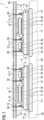
- FIG 2 shows a schematic representation of a second embodiment of a power module 2 in a top view.
- the heat sink 26 is configured, for example by cooling fins, for a gaseous coolant to flow in a coolant flow direction 44, wherein the coolant flow direction 44 runs substantially parallel to the surface 24 of the heat sink 26.
- the gaseous coolant is, for example, air which flows via a fan in the coolant flow direction 44 over the cooling fins of the heat sink 26.
- the power module 2 has, for example, two power units 4, which are spaced apart on the surface 24 of the heat sink 26 in such a way that optimal heat dissipation of the power semiconductors 6 takes place through heat spreading.
- the power units 4 have a rectangular base area with identical dimensions x, y.
- the power units 4 viewed transversely to the coolant flow direction 44, are arranged offset by a first transverse offset x1.
- the power units 4, viewed in the coolant flow direction 44 are spaced apart by a longitudinal offset y1. Due to the size of the surface 24 of the heat sink 26, the transverse offset x1 and the longitudinal offset y1 are smaller than the respective dimensions x, y of the power unit 4. Due to the cohesive connection of the power units 4 to the heat sink 26, fewer assembly points 46 are required.
- each power unit 4 is assigned two mounting points 46, with the heat sink 26 having at least two mounting points 46, in particular at least four mounting points 46.
- the further version of the power module 2 in FIG 2 corresponds to the version in FIG 1 .
- FIG 3 shows a schematic representation of a third embodiment of a power module 2 in a top view, the two power units 4 having a common housing 48.
- the two power units 4 of the power module 2 are electrically connected to one another via a bond connection 34, the bond connection 34 having a plurality of bonding wires, ribbon bonds and/or other means for producing the bond connection 34.
- the housing 48 includes a half-bridge circuit for high-current applications, with two half-bridges, each associated with a power unit 4, being connected in parallel to drive a higher load current.
- the further version of the power module 2 in FIG 3 corresponds to the version in FIG 2 .
- FIG 4 shows a schematic representation of a fourth embodiment of a power module 2 in a top view, wherein the power module 2 includes three power units 4.
- a distance x1, x2, y1, y2 between the power units 4 varies in the coolant flow direction 44 and transversely to the coolant flow direction 44.
- These are arranged in such a way that the distance y1, y2 between the power units 4 increases in the coolant flow direction 44.
- the further version of the power module 2 in FIG 3 corresponds to the version in FIG 2 .
- FIG 5 shows a schematic representation of a fifth embodiment of a power module 2 in a top view, in which, in addition to the variation of the distances x1, x2, y1, y2 between the power units 4, additional heat spreading is achieved by different arrangements of the components on the substrates 8.
- the power semiconductors 6 with the freely positionable contacts 38 are arranged on the respective substrates in such a way that optimal heat dissipation of the power semiconductors 4 takes place.
- the area of the respective substrates 8 can be varied for greater heat spread.
- the further version of the power module 2 in FIG 5 corresponds to the version in FIG 4 .
- FIG 6 shows a schematic three-dimensional representation of a sixth embodiment of a power module 2, wherein the power module 2 comprises three power units 4.
- the power units 4 each have a housing 48 with a housing cover 50, the housing cover 50 being shown transparently in the front power unit 4.
- the heat sink has a base plate 51 with cooling fins 52 arranged running in the coolant flow direction 44, the cooling fins 52 being connected to the base plate 51 and the base plate 51 and the cooling fins 52 of the heat sink 26 being made in one piece.
- the base plate 51 has a substantially constant first thickness d1 of 3.5 mm to 5 mm, in particular 3.5 mm to 4 mm, while the ribs have a second thickness d2, which is smaller than the first thickness d1 of the base plate 51 is.
- the cooling fins 52 are arranged equidistantly transversely to the coolant flow direction 44.
- the heat sink 26 is made by extrusion from an aluminum alloy, which contains, for example, silicon from 0.1% to 1.0%, in particular from 0.1% to 0.6%. Furthermore, the cooling fins 52 are arranged such that a ratio of a length l of the cooling fins 52 to a distance a between the cooling fins 52 is at least 10: l/a ⁇ 10.
- the further version of the power module 2 in FIG 6 corresponds to the version in FIG 4 .
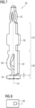
- FIG 7 shows a three-dimensional representation of a freely positionable contact 38.
- the freely positionable contact 38 has a press-in zone 53, which can be connected to the power board 36 and is designed asymmetrically with respect to a force center line 54, with a press-in force in the force center line 54 freely positionable contact 38 can be initiated.
- Positioning aids 56 for aligning the freely positionable contact 38 for example in a soldering jig, are mounted in a central part 55.
- a lower part 58 of the freely positionable contact 38 is designed as an asymmetrical relief section which has an elastically yielding section 60 and a stop 62 arranged parallel thereto, the stop being spaced from a foot 64 by a gap width s.
- the foot 64 is configured for a cohesive connection, for example by soldering or sintering.
- the freely positionable contact 38 is materially connected to the upper metallization 18 of a substrate 8 via the foot 64.
- the elastically yielding section 60 has an S-shaped spring shape with a defined spring travel. In this way, forces occurring during the press-in process or during operation, which are caused, for example, by vibrations, can be absorbed in the relief section. In addition, tolerances can be compensated for due to the elasticity. In particular, a spring constant of the elastically yielding section 60 is produced with the aid of a cross-sectional reduction by punching.
- the further version of the freely positionable contact 38 in FIG 7 corresponds to the version in FIG 1 .
- FIG 8 shows a schematic representation of a power converter 66 with a power module 2.
- the power converter 66 can include more than one power module 2.
- the invention relates to a power module 2 with at least three power units 4, each of which comprises at least one power semiconductor 6 and a substrate 8.
- the at least one power semiconductor 6 is connected, in particular cohesively, to the respective substrate 8, the substrates 8 of the at least two power units 4 each being directly cohesively connected to one Surface 24 of a common heat sink 26 are connected.
Description
- Die Erfindung betrifft ein Leistungsmodul mit mindestens drei Leistungseinheiten.
- Darüber hinaus betrifft die Erfindung einen Stromrichter mit mindestens einem derartigen Leistungshalbleitermodul.
- In derartigen Stromrichtern werden in der Regel, insbesondere durch ein Gehäuse, abgeschlossene Schalter-Module, die derzeit in diskreten Bauformen gefertigt werden, beispielweise über eine massive metallische Bodenplatte, auf einen Kühlkörper aufgeschraubt. Unter einem Stromrichter ist beispielsweise ein Gleichrichter, ein Wechselrichter, ein Umrichter oder ein Gleichspannungswandler zu verstehen.
- Die Offenlegungsschrift
DE 10 2009 001 722 A1 beschreibt ein Leistungshalbleitermodul, dessen Bodenplatte als Mehrschichtsubstrat ausgebildet und mit einer ausgehärteten Wärmeleitpaste versehen ist, und das mit einem Kühlkörper in thermischen Kontakt gebracht wird. - Die Offenlegungsschrift
DE 10 2010 022 562 A1 beschreibt ein elektrisches Leistungsmodul zur Montage auf einer Leiterplatte, umfassend eine erste Seite zur Montage auf einer Oberfläche einer Wärmesenke, wobei die erste Seite in einer montierten Position des elektrischen Leistungsmoduls auf der Wärmesenke im Wesentlichen parallel zur Wärmesenke angeordnet ist, und eine mit elektrischen Verbindungselementen versehene zweite Seite, wobei die elektrischen Verbindungselemente angepasst sind, das elektrische Leistungsmodul mit der Leiterplatte elektrisch zu verbinden. Das elektrische Leistungsmodul kann auf einfachere Weise mit der Leiterplatte und der Wärmesenke verbunden werden, wenn das elektrische Leistungsmodul mindestens ein dübelartiges Befestigungselement umfasst oder angepasst ist, mindestens ein dübelartiges Befestigungselement aufzunehmen, das in mindestens eine Bohrung der Wärmesenke einführbar ist und angepasst ist, ein Festklemmelement so aufzunehmen, dass das Festklemmelement durch seine Einführung in das mindestens eine dübelartige Befestigungselement in der mindestens einen Bohrung der Wärmesenke festklemmt. - Die Offenlegungsschrift
EP 3 624 184 A1 beschreibt ein Verfahren zur Herstellung einer Leistungsmoduleinheit, wobei eine Grundplatte mit Aussparungen versehen wird. Die Grundplatte wird mit einem Substrat, welches den Leistungshalbleiter trägt, verbunden. Nach der Befestigung des Substrates auf der Grundplatte werden die Kühlrippen in die Aussparungen der Grundplatte geführt und formschlüssig und/oder kraftschlüssig befestigt. - Die Patentschrift
DE 10 2008 007 310 B4 beschreibt einen elektrischen Einpresskontakt, insbesondere Einpressstiftkontakt, zur Übertragung von elektrischem Strom und/oder elektrischen Signalen, mit einem Einpressabschnitt und einem Montageabschnitt, die über einen Entlastungsabschnitt miteinander mechanisch gekoppelt sind, und der Entlastungsabschnitt einen Ausgleichsbereich und einen Anschlagbereich aufweist, wobei der Ausgleichsbereich eine gekoppelte Relativbewegung des Einpressabschnitts und des Montageabschnitts zulässt, und der Anschlagbereich eine Aufeinanderzubewegung von Einpressabschnitt und Montageabschnitt blockiert, und wobei der Anschlagbereich des Entlastungsabschnitts symmetrisch bezüglich einer Kraftmittellinie des elektrischen Einpresskontakts angeordnet ist, entlang welcher eine Einpresskraft in den elektrischen Einpresskontakt einleitbar ist, die aus einem Einpressen des elektrischen Einpresskontakts in einen Träger resultiert. - Die Offenlegungsschrift
US 2020/0185302 A1 beschreibt ein Leistungsmodul mit niedriger Induktivität für ultraschnelle Halbleiter-Leistungsschaltgeräte mit breiter Bandlücke. Leiterbahnen definieren Leistungsbusse für eine Schalttopologie, z.B. mit GaN E-HEMTs, wobei sich die Leistungsanschlüsse von den Leistungsbussen durch das Gehäuse erstrecken, um einen Abstand zwischen Heatsink und Busbar zu schaffen, der die Kriech- und Luftanforderungen erfüllt. - Die
WO 2007/065666 A2 beschreibt ein elektrisches Gerät umfassend Wärme erzeugende elektrische Komponenten, insbesondere Leistungshalbleiter, und eine Kühlvorrichtung zur Abfuhr dieser Wärme, wobei die Kühlvorrichtung aus einem Luftkühler gebildet ist, an dem ein Flüssigkeitskühler anmontiert ist, wobei der Luftkühler zwischen dem Flüssigkeitskühler und den Wärme erzeugenden elektrischen Komponenten vorgesehen ist. - Die Offenlegungsschrift
EP 3 273 471 A1 beschreibt ein Leistungsmodul mit mindestens drei Leistungseinheiten welche jeweils mindestens einen Leistungshalbleiter und ein Substrat mit einer Oberfläche eines gemeinsamen Kühlkörpers verbunden sind, wobei der Kühlkörper konfiguriert ist, dass ein gasförmiges Kühlmittel in eine Kühlmittelströmungsrichtung strömt, wobei die Kühlmittelströmungsrichtung im Wesentlichen parallel zur Oberfläche des Kühlkörpers verläuft, wobei die Leistungseinheiten quer zur Kühlmittelströmungsrichtung versetzt angeordnet sind. 1 - Vor diesem Hintergrund ist es eine Aufgabe der vorliegenden Erfindung, den erforderlichen Bauraum von Leistungsmodulen zu verringern und eine Entwärmung zu verbessern.
- Die Aufgabe wird erfindungsgemäß gelöst durch ein Leistungsmodul mit mindestens drei Leistungseinheiten, welche jeweils mindestens einen Leistungshalbleiter und ein Substrat umfassen, wobei der jeweils mindestens eine Leistungshalbleiter, insbesondere stoffschlüssig, mit dem jeweiligen Substrat verbunden ist, wobei die Substrate der mindestens drei Leistungseinheiten jeweils unmittelbar stoffschlüssig mit einer Oberfläche eines gemeinsamen Kühlkörpers verbunden sind, wobei der Kühlkörper konfiguriert ist, dass ein gasförmiges Kühlmittel in eine Kühlmittelströmungsrichtung strömt, wobei die Kühlmittelströmungsrichtung im Wesentlichen parallel zur Oberfläche des Kühlkörpers verläuft, wobei die Leistungseinheiten quer zur Kühlmittelströmungsrichtung versetzt angeordnet sind, wobei der Kühlkörper in eine Kühlmittelströmungsrichtung verlaufend angeordnete Kühlrippen aufweist, wobei ein im Wesentlichen parallel zur Oberfläche des Kühlkörpers verlaufend angeordnetes Power-Board über frei positionierbare Kontakte mit den Leistungseinheiten verbunden ist.
- Darüber hinaus wird die Aufgabe erfindungsgemäß durch einen Stromrichter mit zumindest einem derartigen Leistungsmodul gelöst.
- Die in Bezug auf das Leistungsmodul nachstehend angeführten Vorteile und bevorzugten Ausgestaltungen lassen sich sinngemäß auf den Stromrichter übertragen.
- Der Erfindung liegt die Überlegung zugrunde, den Platzbedarf eines Leistungsmoduls durch Reduzierung der Anzahl thermischer Schnittstellen zu verringern und dabei eine verbesserte Entwärmung zu erreichen. Ein derartiges Leistungsmodul weist mindestens drei Leistungseinheiten auf, wobei die Leistungseinheiten jeweils mindestens einen Leistungshalbleiter und ein Substrat umfassen. Ein Substrat ist eine beidseitig metallisierte dielektrische Materiallage, wobei die dielektrische Materiallage beispielsweise eine Dicke d von 25 µm bis 400 µm, insbesondere 50 µm bis 250 µm, aufweist. Ferner enthält die dielektrische Materiallage einen keramischen Werkstoff, beispielsweise Aluminiumnitrid oder Aluminiumoxid, oder einen organischen Werkstoff, beispielsweise einem Polyamid. Insbesondere enthält die Metallisierung Kupfer, Molybdän, Gold und/oder Silber. Ferner kann zumindest eine Seite der Metallisierung des Substrats strukturiert ausgebildet sein. Der Leistungshalbleiter ist insbesondere als ein Transistor und/oder eine Diode, ausgeführt, wobei der Transistor beispielsweise als Insulated-Gate-Bipolar-Transistor (IGBT), als Metalloxide-Semiconductor-Field-Effect-Transistor (MOSFET) oder als ein Feldeffekttransistor ausgeführt ist. Der jeweils mindestens eine Leistungshalbleiter ist, insbesondere stoffschlüssig, z.B. über eine Sinterverbindung oder Lötverbindung, mit dem jeweiligen Substrat verbunden.
- Die Substrate der Leistungseinheiten sind jeweils, insbesondere mit einer dem mindestens einen Leistungshalbleiter abgewandten Seite, unmittelbar stoffschlüssig mit einer Oberfläche eines gemeinsamen Kühlkörpers verbunden. Unter einer unmittelbar stoffschlüssigen Kontaktierung ist eine direkte Kontaktierung zu verstehen, die Verbindungsmittel zur Herstellung der stoffschlüssigen Verbindung wie Kleber, Lötzinn, Sinterpaste, ... einschließt, ein zusätzliches Verbindungselement wie einen zusätzlichen Leiter, einen Bonddraht, einen Abstandshalter, eine Bodenplatte, Wärmeleitpaste, ... jedoch ausschließt. Durch den Wegfall eines derartigen zusätzlichen Verbindungselements wird eine verbesserte thermische Anbindung der Leistungshalbleiter erreicht, sodass eine verbesserte Entwärmung stattfindet. Darüber hinaus wird durch die unmittelbar stoffschlüssige Verbindung Bauraum eingespart. Durch eine stoffschlüssige Verbindung von mindestens drei Leistungseinheiten auf einem gemeinsamen Kühlkörper ergibt sich eine hohe Flexibilität hinsichtlich der Positionierung der Leistungseinheiten auf der Oberfläche des Kühlkörpers, um durch Wärmespreizung eine optimierte Entwärmung zu erzielen und die Oberfläche des Kühlkörpers maximal auszunutzen.
- Der Kühlkörper ist konfiguriert, dass ein gasförmiges Kühlmittel in eine Kühlmittelströmungsrichtung strömt, wobei die Kühlmittelströmungsrichtung im Wesentlichen parallel zur Oberfläche des Kühlkörpers verläuft. Das gasförmige Kühlmittel ist beispielsweise Luft. Insbesondere wird das Leistungsmodul einseitig durch einen Lüfter gekühlt, der in fluidtechnischer Verbindung mit den Kühlrippen des Kühlkörpers steht, sodass die Luft vom Lüfter im Wesentlichen parallel zur Oberfläche des Kühlkörpers über die Kühlrippen des Kühlkörpers strömt. Eine derartige Konfiguration ist kostengünstig und zuverlässig.
- Die mindestens drei Leistungseinheiten sind quer zur Kühlmittelströmungsrichtung versetzt angeordnet. Durch eine versetzte Anordnung wird eine Wärmespreizung erreicht, die zu einer optimalen Entwärmung führt.
- Unter einem Power-Board ist eine Leiterplatte zu verstehen, welche z.B. als, insbesondere mehrlagig ausgeführtes, Printed-Circuit-Board (PCB) ausgeführt ist. Die Leiterplatte enthält beispielsweise eine Schnittstelle zu den Leistungseinheiten, eine Treiberschaltung, eine Ansteuerschaltung, und/oder Kondensatoren. Unter einem frei positionierbaren Kontakt ist beispielsweise ein Pin zu verstehen, der durch seine strukturellen Eigenschaften frei auf einem Substrat angeordnet werden kann. Derartige strukturelle Eigenschaften sind beispielsweise ein Fuß, der es dem Pin, beispielsweise durch eine stoffschlüssige Verbindung mit dem Substrat, erlaubt, ohne ein Gehäuse oder andere Stabilisierungsmittel frei und stabil auf dem Substrat angeordnet zu werden und/oder ein Taumelkreis, der eine Findung einer Bohrung im Power-Board erleichtert und für mehr Stabilität und Robustheit, z.B. bei einer thermischen Ausdehnung während des Betriebes, sorgt.
- Ein derartiger Kontakt ist beispielsweise aus Kupfer oder einer Kupferlegierung hergestellt, um einen geringen Widerstand und eine hohe Stromtragfähigkeit zu erreichen. Durch die freie Positionierbarkeit der Kontakte werden kurze Leitungswege und damit verbundene niedrige Induktivitäten erreicht, was Leistungseinheiten mit niedrigen Impedanzen und geringen Verlusten ermöglicht. Ferner wird kostengünstig und einfach ein zellindividuelles Design der Leistungseinheiten ermöglicht.
- Eine weitere Ausführungsform sieht vor, dass die Substrate der Leistungseinheiten jeweils eine dielektrische Materiallage mit einer Wärmeleitfähigkeit von mindestens 25 W.m-1.K-1, insbesondere mindestens 100 W.m-1.K-1, und einer Dicke von 25 µm bis 400 µm, insbesondere 50 µm bis 250 µm, aufweisen. Beispielsweise ist die dielektrische Materiallage aus Aluminiumnitrid oder Aluminiumoxid hergestellt. Insbesondere durch die mehreren stoffschlüssig auf der Kühlkörperoberfläche verbundener Substrate wird eine Verwendung von derartig dünnen keramischen Schichten ermöglicht, was zu einer Verbesserung der thermischen Anbindung der Leistungshalbleiter führt.
- Eine weitere Ausführungsform sieht vor, dass mindestens zwei der Leistungseinheiten ein gemeinsames Gehäuse aufweisen. Ein derartiges gemeinsames Gehäuse ist beispielsweise aus einem Kunststoff hergestellt. Durch das gemeinsame Gehäuse wird Bauraum eingespart.
- Eine weitere Ausführungsform sieht vor, dass mindestens zwei der Leistungseinheiten, insbesondere über eine Bondverbindung, elektrisch leitend miteinander verbunden sind. Eine derartige Bondverbindung wird beispielsweise über Bonddrähte oder Ribbon-Bonds hergestellt. Beispielsweise sind identische Leistungseinheiten über die Bondverbindung parallel zusammenschaltbar, um einen höheren Laststrom zu treiben. Durch einen derartigen modularen Aufbau können Leistungsmodule kostengünstig skalierbar hergestellt werden.
- Eine weitere Ausführungsform sieht vor, dass der Kühlkörper, welcher aus einem ersten metallischen Werkstoff hergestellt ist, auf seiner Oberfläche zumindest eine Kavität aufweist, die mit einem zweiten metallischen Werkstoff gefüllt ist, welcher eine höhere Wärmeleitfähigkeit als der erste metallische Werkstoff aufweist, wobei zumindest ein Substrat einer Leistungseinheit unmittelbar stoffschlüssig mit dem zweiten metallischen Werkstoff verbunden ist, aufweist. Beispielsweise ist der erste metallische Werkstoff Aluminium und der zweite metallische Werkstoff Kupfer. Durch eine mit dem zweiten metallischen Werkstoff gefüllte Kavität wird eine verbesserte thermische Anbindung der Leistungseinheiten an dem Kühlkörper erreicht.
- Eine weitere Ausführungsform sieht vor, dass der zweite metallische Werkstoff im Wesentlichen planbündig mit der Oberfläche des Kühlkörpers abschließt. Unter einem planbündig mit der Oberfläche des Kühlkörpers ausgestalteten Abschluss ist ein ebener und im Wesentlichen zur Kühlkörperoberfläche stetiger Abschluss der Füllung der Kavität zu verstehen. Insbesondere bildet der zweite metallische Werkstoff eine ebene Oberfläche aus, die im Wesentlichen nahtlos in die Kühlkörperoberfläche übergeht. Durch eine derartige ebene Ausführung wird eine optimale thermische Anbindung an den Kühlkörper erreicht und es werden mechanische und/oder thermische Spannungen im mit dem zweiten metallischen Werkstoff verbundenen Substrat vermieden.
- Eine weitere Ausführungsform sieht vor, dass jeder der mindestens zwei Leistungseinheiten eine mit dem zweiten metallischen Werkstoff gefüllte Kavität zugewiesen ist. Die mit dem zweiten metallischen Werkstoff gefüllten Kavitäten sind beispielsweise als Inseln ausgeführt, die eine größere Fläche aufweisen als die jeweiligen Substrate und an jeder der Substratkanten über das Substrat überstehen, wodurch eine verbesserte thermische Anbindung der Leistungseinheiten an dem Kühlkörper erreicht wird.
- Eine weitere Ausführungsform sieht vor, dass der zweite metallische Werkstoff mittels eines additiven Verfahrens in die zumindest eine Kavität eingebracht ist. Beispielsweise ist der zweite metallische Werkstoff mittels Kaltgasspritzen in die zumindest eine Kavität eingebracht. Das additive Verfahren erlaubt, insbesondere im Vergleich zu einem Gießverfahren, eine sehr geringe Stärke des ersten metallischen Werkstoffs unterhalb der Kavität, sodass sich die Kühlrippen sehr nahe am zweiten metallischen Werkstoff, der eine höhere Wärmeleitfähigkeit als der erste metallische Werkstoff aufweist, befinden, sodass eine verbesserte thermische Anbindung an ein Kühlfluid erreicht wird.
- Eine weitere Ausführungsform sieht vor, dass die Leistungseinheiten derartig auf der Oberfläche des Kühlkörpers angeordnet sind, dass durch Wärmespreizung eine optimale Entwärmung der Leistungshalbleiter stattfindet. Die Leistungseinheiten sind auf dem Kühlkörper, insbesondere in Relation zu einer Strömungsrichtung eines Kühlmittels, so orientiert und beabstandet, dass die in den Leistungshalbleitern der Leistungseinheiten, insbesondere näherungsweise punktuell, entstehende Abwärme möglichst gleichmäßig auf der Oberfläche des Kühlkörpers verteilt wird und so eine Wärmespreizung stattfindet. Durch eine derartige Anordnung wird eine höhere Robustheit des Leistungsmoduls während des Betriebes erreicht.
- Eine weitere Ausführungsform sieht vor, dass ein Abstand zwischen den Leistungseinheiten in Kühlmittelströmungsrichtung und/oder quer zur Kühlmittelströmungsrichtung variiert. Beispielsweise ist jeweils eine Leistungseinheit einer Phase eines dreiphasigen Systems zugeordnet. Durch Variation der Abstände in Kühlmittelströmungsrichtung und/oder quer zur Kühlmittelströmungsrichtung wird durch Wärmespreizung eine optimale Entwärmung erreicht.
- Eine weitere Ausführungsform sieht vor, dass ein Abstand zwischen den Leistungseinheiten in Kühlmittelströmungsrichtung zunimmt. Da sich das Kühlmittel in Kühlmittelströmungsrichtung unterhalb der Leistungseinheiten erwärmt, wird durch eine zunehmende Entfernung eine bessere Durchmischung von stark und schwach erwärmtem Kühlmittel erreicht. Ferner wird zumindest eine höhere Abkühlung bei zunehmendem Abstand erreicht, sodass in Kühlmittelströmungsrichtung zunehmende Abstände zu einer gleichmäßigeren Temperaturverteilung auf dem Kühlkörper führen.
- Eine weitere Ausführungsform sieht vor, dass die frei positionierbaren Kontakte stoffschlüssig mit den jeweiligen Substraten der Leistungseinheiten verbunden sind. Beispielsweise sind die frei positionierbaren Kontakte auf den jeweiligen Substraten aufgelötet und mittels einer Presspass-Verbindung mit dem Power-Board verbunden.
- Eine weitere Ausführungsform sieht vor, dass die frei positionierbaren Kontakte bezogen auf eine Kraftmittellinie asymmetrisch ausgeführt sind. Entlang der Kraftmittellinie ist eine Einpresskraft in den frei positionierbaren Kontakt einleitbar. Eine asymmetrische Ausgestaltung der frei positionierbaren Kontakte erlaubt es, einen höheren Leiterquerschnitt bei gleichzeitig geringeren Werkzeugkosten im Vergleich zum Stand der Technik umzusetzen, wodurch die Stromtragfähigkeit der Kontakte erhöht wird.
- Eine weitere Ausführungsform sieht vor, dass der Kühlkörper aus einer Aluminiumlegierung mit einem Siliziumanteil bis 1,0 %, insbesondere bis 0,6 %, mittels Strangpressen hergestellt ist. Insbesondere im Vergleich zu einem gegossenen Kühlkörper, wird durch einen stranggepressten Kühlkörper eine verbesserte Wärmeleitfähigkeit erreicht, da beim Strangpressen ein niedriger Siliziumanteil verwendbar ist. Ein stranggepresster Kühlkörper, welcher aus einer derartigen Aluminiumlegierung hergestellt ist, führt zu einer verbesserten Wärmespreizung.
- Eine weitere Ausführungsform sieht vor, dass die Kühlrippen derartig angeordnet sind, dass ein Verhältnis einer Länge der Kühlrippen zu einem Abstand zwischen den Kühlrippen mindestens 10 beträgt. Ein derartiges Verhältnis ist beispielsweise mittels Strangpressen erreichbar, wobei, insbesondere mit einem stranggepressten Kühlkörper, eine optimale Entwärmung erreicht wird. Ferner werden bei einem derartigen Verhältnis kurze Kühlrippen, beispielsweise mit einer Länge von 20 mm bis 30 mm, ermöglicht, sodass das Leistungsmodul mit dem Kühlkörper in einem Lötofen, insbesondere automatisiert, verarbeitbar ist, was die Herstellung des Leistungsmoduls einfacher und kostengünstiger macht.
- Eine weitere Ausführungsform sieht vor, dass der Kühlkörper eine Basisplatte mit einer im Wesentlichen konstanten ersten Dicke von 3,5 mm bis 5 mm, insbesondere 3,5 mm bis 4 mm, aufweist, wobei die Basisplatte und die Kühlrippen des Kühlkörpers einstückig ausgeführt sind. Eine derartig dünne Basisplatte, welche beispielsweise mittels Strangpressen herstellbar ist, führt zu einer verbesserten Entwärmung. Ferner wird durch eine derartig dünne Basisplatte eine Gesamthöhe des Leistungsmoduls verringert, sodass das Leistungsmodul mit dem Kühlkörper in einem Lötofen, insbesondere automatisiert, verarbeitbar ist, was die Herstellung des Leistungsmoduls einfacher und kostengünstiger macht.
- Im Folgenden wird die Erfindung anhand der in den Figuren dargestellten Ausführungsbeispiele näher beschrieben und erläutert.
- Es zeigen:
- FIG 1
- eine schematische Darstellung einer ersten Ausgestaltung eines Leistungsmoduls im Querschnitt,
- FIG 2
- eine schematische Darstellung einer zweiten Ausgestaltung eines Leistungsmoduls in einer Draufsicht,
- FIG 3
- eine schematische Darstellung einer dritten Ausgestaltung eines Leistungsmoduls in einer Draufsicht,
- FIG 4
- eine schematische Darstellung einer vierten Ausgestaltung eines Leistungsmoduls in einer Draufsicht,
- FIG 5
- eine schematische Darstellung einer fünften Ausgestaltung eines Leistungsmoduls in einer Draufsicht,
- FIG 6
- eine schematische dreidimensionale Darstellung einer sechsten Ausgestaltung eines Leistungsmoduls,
- FIG 7
- eine dreidimensionale Darstellung eines frei positionierbaren Kontaktes,
- FIG 8
- eine schematische Darstellung eines Stromrichters mit einem Leistungsmodul.
- Bei den im Folgenden erläuterten Ausführungsbeispielen handelt es sich um bevorzugte Ausführungsformen der Erfindung. Bei den Ausführungsbeispielen stellen die beschriebenen Komponenten der Ausführungsformen jeweils einzelne, unabhängig voneinander zu betrachtende Merkmale der Erfindung dar, welche die Erfindung jeweils auch unabhängig voneinander weiterbilden und damit auch einzeln oder in einer anderen als der gezeigten Kombination als Bestandteil der Erfindung anzusehen sind. Des Weiteren sind die beschriebenen Ausführungsformen auch durch weitere der bereits beschriebenen Merkmale der Erfindung ergänzbar.
- Gleiche Bezugszeichen haben in den verschiedenen Figuren die gleiche Bedeutung.
-
FIG 1 zeigt eine schematische Darstellung einer ersten Ausgestaltung eines Leistungsmoduls 2 im Querschnitt. Das Leistungsmodul 2 weist beispielhaft zwei Leistungseinheiten 4 auf, welche jeweils Leistungshalbleiter 6 und ein Substrat 8 umfassen. Die Leistungshalbleiter 6 sind als Transistor 10 oder als Diode 12 ausgeführt, wobei der Transistor 10 beispielsweise als Insulated-Gate-Bipolar-Transistor (IGBT), als Metalloxide-Semiconductor-Field-Effect-Transistor (MOSFET) oder als Feldeffekttransistor ausgeführt ist. Beispielsweise ist jedem der Transistoren 10 eine, insbesondere antiparalelle, Diode 12 zugewiesen. - Die Substrate 8 der beiden Leistungseinheiten 4 weisen eine dielektrische Materiallage 14 auf, die einen keramischen Werkstoff, beispielsweise Aluminiumnitrid oder Aluminiumoxid, oder einen organischen Werkstoff, beispielsweise einem Polyamid enthält. Die dielektrische Materiallage 14 weist eine Dicke d von 25 µm bis 400 µm, insbesondere 50 µm bis 250 µm, auf. Darüber hinaus weisen die Substrate 8 jeweils auf einer den Leistungshalbleitern 6 zugewandten Seite 16 eine, insbesondere strukturierte, obere Metallisierung 18 und auf einer den Leistungshalbleitern 6 abgewandten Seite 20 eine untere Metallisierung 22 auf, wobei die Substrate 8 jeweils unmittelbar stoffschlüssig mit einer Oberfläche 24 eines gemeinsamen Kühlkörpers 26 verbunden sind. Die obere Metallisierung 18 und die untere Metallisierung 22 sind beispielsweise aus Kupfer hergestellt. Die stoffschlüssige Verbindung 28 zum Kühlkörper 26 wird durch Löten oder Sintern hergestellt. Unter einer unmittelbar stoffschlüssigen Kontaktierung ist eine direkte Kontaktierung zu verstehen, die Verbindungsmittel zur Herstellung der stoffschlüssigen Verbindung wie Kleber, Lötzinn, Sinterpaste, ... einschließt, ein zusätzliches Verbindungselement wie einen zusätzlichen Leiter, einen Bonddraht, einen Abstandshalter, eine Bodenplatte, Wärmeleitpaste, ... jedoch ausschließt. Eine dem Substrat 8 zugewandte Seite 30 der Leistungshalbleiter 6 ist jeweils ebenfalls über eine stoffschlüssige Verbindung 28, die durch Löten oder Sintern hergestellt wird, mit der oberen Metallisierung 18 des Substrats 8 verbunden. Eine dem Substrat 8 abgewandte Seite 32 der Leistungshalbleiter 6 ist jeweils über eine Bondverbindung 34 mit der oberen Metallisierung 18 des Substrats 8 verbunden. Die Bondverbindung 34 umfasst beispielsweise mindestens einen Bonddraht, mindestens einen Ribbon-Bond und/oder andere Mittel zur Herstellung einer Bondverbindung.
- Die Transistoren 10 in
FIG 1 sind beispielhaft als IGBTs ausgeführt, deren Kollektor-Kontakt C auf der dem Substrat 8 zugewandte Seite 30 der Leistungshalbleiter 6 jeweils über eine stoffschlüssige Verbindung 28 mit der oberen Metallisierung 18 des Substrats 8 verbunden sind. Die Emitter-Kontakte E der als IGBTs ausgeführten Transistoren 10 sind, davon elektrisch isoliert, über Bondverbindungen 34 mit der oberen Metallisierung 18 des Substrats 8 verbunden. Die Gate-Kontakte der Transistoren 10 und die Bondverbindungen der Dioden 12 sind aus Gründen der Übersichtlichkeit inFIG 1 nicht dargestellt. - Ein im Wesentlichen parallel zur Oberfläche 24 des Kühlkörpers 26 verlaufend angeordnetes Power-Board 36 ist über frei positionierbare Kontakte 38 mit den Leistungseinheiten 4 verbunden, wobei die frei positionierbaren Kontakte 38 stoffschlüssig mit den oberen Metallisierungen 18 der jeweiligen Substrate 8 der Leistungseinheiten 4 verbunden sind. Die frei positionierbaren Kontakte 38 weisen einen elastisch nachgebenden Abschnitt auf und sind beispielsweise mit einer Presspass-Verbindung mit dem Power-Board 36 verbunden.
- Der Kühlkörper 26 ist aus einem ersten metallischen Werkstoff 39 hergestellt. Auf seiner Oberfläche 24 sind Kavitäten 40 eingebracht, die mit einem zweiten metallischen Werkstoff 42 gefüllt sind, wobei der zweite metallische Werkstoff 42 eine höhere Wärmeleitfähigkeit als der erste metallische Werkstoff 39 aufweist. Beispielsweise ist der erste metallische Werkstoff 39 Aluminium und der zweite metallische Werkstoff 42 Kupfer. Jeder der mindestens zwei Leistungseinheiten 4 ist eine mit dem zweiten metallischen Werkstoff 42 gefüllte Kavität 40 zugewiesen, wobei der zweite metallische Werkstoff 42 im Wesentlichen planbündig mit der Oberfläche 24 des Kühlkörpers 26 abschließt und die unteren Metallisierungen 22 des jeweiligen Substrats 8 stoffschlüssig mit dem zweiten metallischen Werkstoff 42 verbunden sind. Insbesondere ist der zweite metallische Werkstoff 42 mittels eines additiven Verfahrens, beispielsweise mittels Kaltgasspritzen, in die Kavitäten eingebracht. Jeder der Leistungseinheiten 4 kann ein dedizierter Sensor, insbesondere Temperatursensor, zugewiesen sein, um die Temperatur der Leistungshalbleiter 6 zu überwachen.
-
FIG 2 zeigt eine schematische Darstellung einer zweiten Ausgestaltung eines Leistungsmoduls 2 in einer Draufsicht. Der Kühlkörper 26 ist, beispielsweise durch Kühlrippen, dafür konfiguriert, dass ein gasförmiges Kühlmittel in eine Kühlmittelströmungsrichtung 44 strömt, wobei die Kühlmittelströmungsrichtung 44 im Wesentlichen parallel zur Oberfläche 24 des Kühlkörpers 26 verläuft. Das gasförmige Kühlmittel ist beispielsweise Luft, die über einen Lüfter in die Kühlmittelströmungsrichtung 44 über die Kühlrippen des Kühlkörpers 26 strömt. Das Leistungsmodul 2 weist beispielhaft zwei Leistungseinheiten 4 auf, die derartig auf der Oberfläche 24 des Kühlkörpers 26 beabstandet sind, dass durch Wärmespreizung eine optimale Entwärmung der Leistungshalbleiter 6 stattfindet. Ferner weisen die Leistungseinheiten 4 eine rechteckige Grundfläche mit identischen Abmessungen x, y auf. Um eine optimale Entwärmung der Leistungshalbleiter 6 zu erreichen sind die Leistungseinheiten 4, quer zur Kühlmittelströmungsrichtung 44 betrachtet, um einen ersten Querversatz x1 versetzt angeordnet. Darüber hinaus sind die Leistungseinheiten 4, in Kühlmittelströmungsrichtung 44 gesehen, um einen Längsversatz y1 beabstandet. Aufgrund der Größe der Oberfläche 24 des Kühlkörpers 26 sind der Querversatz x1 und der Längsversatz y1 kleiner als die jeweiligen Abmessungen x, y der Leistungseinheit 4. Durch die stoffschlüssige Verbindung der Leistungseinheiten 4 mit dem Kühlkörper 26 sind weniger Montagepunkte 46 erforderlich. Beispielhaft sind jeder Leistungseinheit 4 zwei Montagepunkte 46 zugeordnet, wobei der Kühlkörper 26 mindestens zwei Montagepunkte 46, insbesondere mindestens vier Montagepunkte 46, aufweist. Die weitere Ausführung des Leistungsmoduls 2 inFIG 2 entspricht der Ausführung inFIG 1 . -
FIG 3 zeigt eine schematische Darstellung einer dritten Ausgestaltung eines Leistungsmoduls 2 in einer Draufsicht, wobei die zwei Leistungseinheiten 4 ein gemeinsames Gehäuse 48 aufweisen. Die beiden Leistungseinheiten 4 des Leistungsmoduls 2 sind über eine Bondverbindung 34 elektrisch leitend miteinander verbunden, wobei die Bondverbindung 34 eine Mehrzahl an Bonddrähten, Ribbon-Bonds und/oder andere Mittel zur Herstellung der Bondverbindung 34 aufweist. Beispielsweise umfasst das Gehäuse 48 eine Halbbrückenschaltung für Hochstromanwendungen, wobei zwei Halbbrücken, die jeweils einer Leistungseinheit 4 zugeordnet sind, parallelgeschaltet sind, um einen höheren Laststrom zu treiben. Die weitere Ausführung des Leistungsmoduls 2 inFIG 3 entspricht der Ausführung inFIG 2 . -
FIG 4 zeigt eine schematische Darstellung einer vierten Ausgestaltung eines Leistungsmoduls 2 in einer Draufsicht, wobei das Leistungsmodul 2 drei Leistungseinheiten 4 umfasst. Ein Abstand x1, x2, y1, y2 zwischen den Leistungseinheiten 4 variiert in Kühlmittelströmungsrichtung 44 und quer zur Kühlmittelströmungsrichtung 44. Um eine im Wesentlichen gleichmäßige Entwärmung der Leistungseinheiten 4 zu gewährleisten, sind diese derartig angeordnet, dass der Abstand y1, y2 zwischen den Leistungseinheiten 4 in Kühlmittelströmungsrichtung 44 zunimmt. Die weitere Ausführung des Leistungsmoduls 2 inFIG 3 entspricht der Ausführung inFIG 2 . -
FIG 5 zeigt eine schematische Darstellung einer fünften Ausgestaltung eines Leistungsmoduls 2 in einer Draufsicht, wobei neben der Variation der Abstände x1, x2, y1, y2 zwischen den Leistungseinheiten 4 eine zusätzliche Wärmespreizung durch unterschiedliche Anordnung der Komponenten auf den Substraten 8 erreicht wird. Insbesondere werden die Leistungshalbleiter 6 mit den frei positionierbaren Kontakten 38 derartig auf den jeweiligen Substraten angeordnet, dass eine optimale Entwärmung der Leistungshalbleiter 4 stattfindet. Die Fläche der jeweiligen Substrate 8 kann für eine größere Wärmespreizung variiert werden. Die weitere Ausführung des Leistungsmoduls 2 inFIG 5 entspricht der Ausführung inFIG 4 . -
FIG 6 zeigt eine schematische dreidimensionale Darstellung einer sechsten Ausgestaltung eines Leistungsmoduls 2, wobei das Leistungsmodul 2 drei Leistungseinheiten 4 umfasst. Die Leistungseinheiten 4 weisen jeweils ein Gehäuse 48 mit einem Gehäusedeckel 50 auf, wobei der Gehäusedeckel 50 bei der vorderen Leistungseinheit 4 transparent dargestellt ist. Der Kühlkörper weist eine Basisplatte 51 mit in Kühlmittelströmungsrichtung 44 verlaufend angeordnete Kühlrippen 52 auf, wobei die Kühlrippen 52 mit der Basisplatte 51 verbunden sind und wobei die Basisplatte 51 und die Kühlrippen 52 des Kühlkörpers 26 einstückig ausgeführt sind. Die Basisplatte 51 weist eine im Wesentlichen konstante erste Dicke d1 von 3,5 mm bis 5 mm, insbesondere 3,5 mm bis 4 mm, auf, während die Rippen eine zweite Dicke d2 aufweisen, welche kleiner als die erste Dicke d1 der Basisplatte 51 ist. Beispielhaft sind die Kühlrippen 52 quer zur Kühlmittelströmungsrichtung 44 äquidistant angeordnet. - Der Kühlkörper 26 ist % mittels Strangpressen aus einer Aluminiumlegierung hergestellt, welche beispielsweise einen Siliziumanteil von 0,1 % bis 1,0 %, insbesondere von 0,1 % bis 0,6 % enthält. Ferner sind die Kühlrippen 52 derartig angeordnet, dass ein Verhältnis einer Länge l der Kühlrippen 52 zu einem Abstand a zwischen den Kühlrippen 52 mindestens 10 beträgt: l/a≥10. Die weitere Ausführung des Leistungsmoduls 2 in
FIG 6 entspricht der Ausführung inFIG 4 . -
FIG 7 zeigt eine dreidimensionale Darstellung eines frei positionierbaren Kontaktes 38. Der frei positionierbare Kontakt 38 weist eine Einpresszone 53 auf, die mit dem Power-Board 36 verbindbar ist und ist, bezogen auf eine Kraftmittellinie 54 asymmetrisch ausgeführt, wobei entlang der Kraftmittellinie 54 eine Einpresskraft in den frei positionierbaren Kontakt 38 einleitbar ist. In einem Mittelteil 55 sind Positionierungshilfen 56 zur Ausrichtung des frei positionierbaren Kontakts 38, beispielsweise in einem Löt-Jig angebracht. Einem Unterteil 58 des frei positionierbaren Kontakts 38 ist als ein asymmetrischer Entlastungsabschnitt ausgeführt, der einen elastisch nachgebenden Abschnitt 60 und einen parallel dazu angeordneten Anschlag 62 aufweist, wobei der Anschlag über eine Spaltweite s von einem Fuß 64 beabstandet ist. Der Fuß 64 ist für eine stoffschlüssige Verbindung, beispielsweise durch Löten oder Sintern, konfiguriert. Insbesondere wird der frei positionierbare Kontakt 38 über den Fuß 64 mit der oberen Metallisierung 18 eines Substrats 8 stoffschlüssig verbunden. Der elastisch nachgebenden Abschnitt 60 weist eine S-förmige Federform mit einem definierten Federweg auf. Somit sind im Entlastungsabschnitt während des Einpressvorgangs oder während des Betriebes auftretende Kräfte, welche beispielsweise durch Erschütterungen verursacht werden, absorbierbar. Darüber hinaus sind durch die Elastizität Toleranzen ausgleichbar. Insbesondere wird eine Federkonstante des elastisch nachgebenden Abschnitts 60 mit Hilfe einer Querschnittsreduzierung durch Stanzen hergestellt. Die weitere Ausführung des frei positionierbaren Kontaktes 38 inFIG 7 entspricht der Ausführung inFIG 1 . -
FIG 8 zeigt eine schematische Darstellung eines Stromrichters 66 mit einem Leistungsmodul 2. Der Stromrichters 66 kann mehr als ein Leistungsmodul 2 umfassen. - Zusammenfassend betrifft die Erfindung ein Leistungsmodul 2 mit mindestens drei Leistungseinheiten 4, welche jeweils mindestens einen Leistungshalbleiter 6 und ein Substrat 8 umfassen. Um den erforderlichen Bauraum des Leistungsmoduls zu verringern und eine Entwärmung zu verbessern, wird vorgeschlagen, dass der jeweils mindestens eine Leistungshalbleiter 6, insbesondere stoffschlüssig, mit dem jeweiligen Substrat 8 verbunden ist, wobei die Substrate 8 der mindestens zwei Leistungseinheiten 4 jeweils unmittelbar stoffschlüssig mit einer Oberfläche 24 eines gemeinsamen Kühlkörpers 26 verbunden sind.
Claims (19)
- Leistungsmodul (2) mit mindestens drei Leistungseinheiten (4), welche jeweils mindestens einen Leistungshalbleiter (6) und ein Substrat (8) umfassen,wobei der jeweils mindestens eine Leistungshalbleiter (6), insbesondere stoffschlüssig, mit dem jeweiligen Substrat (8) verbunden ist,wobei die Substrate (8) der mindestens drei Leistungseinheiten (4) jeweils unmittelbar stoffschlüssig mit einer Oberfläche (24) eines gemeinsamen Kühlkörpers (26) verbunden sind,wobei der Kühlkörper (26) konfiguriert ist, dass ein gasförmiges Kühlmittel in eine Kühlmittelströmungsrichtung (44) strömt,wobei die Kühlmittelströmungsrichtung (44) im Wesentlichen parallel zur Oberfläche (24) des Kühlkörpers (26) verläuft, wobei die Leistungseinheiten (4) quer zur Kühlmittelströmungsrichtung (44) versetzt angeordnet sind,wobei der Kühlkörper (26) in eine Kühlmittelströmungsrichtung (44) verlaufend angeordnete Kühlrippen (52) aufweist,wobei ein im Wesentlichen parallel zur Oberfläche (24) des Kühlkörpers (26) verlaufend angeordnetes Power-Board (36) über frei positionierbare Kontakte (38) mit den Leistungseinheiten (4) verbunden ist.
- Leistungsmodul (2) nach Anspruch 1,
wobei die Substrate (8) der Leistungseinheiten (4) jeweils eine dielektrische Materiallage (14) mit einer Wärmeleitfähigkeit von mindestens 25 W.m-1.K-1, insbesondere mindestens 100 W.m-1.K-1, und einer Dicke d von 25 µm bis 400 µm, insbesondere 50 µm bis 250 µm, aufweisen. - Leistungsmodul (2) nach einem der Ansprüche 1 oder 2,
wobei die Substrate (8) jeweils eine dielektrischen Materiallage (14) mit einer Dicke (d) von 25 µm bis 400 µm, insbesondere 50 µm bis 250 µm, aufweisen. - Leistungsmodul (2) nach einem der vorherigen Ansprüche, wobei mindestens zwei der Leistungseinheiten (4) ein gemeinsames Gehäuse (48) aufweisen.
- Leistungsmodul (2) nach einem der vorherigen Ansprüche, wobei mindestens zwei der Leistungseinheiten (4), insbesondere über eine Bondverbindung (34), elektrisch leitend miteinander verbunden sind.
- Leistungsmodul (2) nach einem der vorherigen Ansprüche, wobei der Kühlkörper (26), welcher aus einem ersten metallischen Werkstoff (39) hergestellt ist, auf seiner Oberfläche (24) zumindest eine Kavität (40) aufweist, die mit einem zweiten metallischen Werkstoff (42) gefüllt ist, welcher eine höhere Wärmeleitfähigkeit als der erste metallische Werkstoff (39) aufweist,
wobei zumindest ein Substrat (8) einer Leistungseinheit (4) unmittelbar stoffschlüssig mit dem zweiten metallischen Werkstoff (42) verbunden ist. - Leistungsmodul (2) nach Anspruch 6,
wobei der zweite metallische Werkstoff (42) im Wesentlichen planbündig mit der Oberfläche (24) des Kühlkörpers (26) abschließt. - Leistungsmodul (2) nach einem der Ansprüche 6 oder 7,
wobei jeder der mindestens zwei Leistungseinheiten (4) eine mit dem zweiten metallischen Werkstoff (42) gefüllte Kavität (40) zugewiesen ist. - Leistungsmodul (2) nach einem der Ansprüche 6 bis 8,
wobei der zweite metallische Werkstoff (42) mittels eines additiven Verfahrens in die zumindest eine Kavität (40) eingebracht ist. - Leistungsmodul (2) nach einem der vorherigen Ansprüche,
wobei ein Abstand (x1, x2, y1, y2) zwischen den Leistungseinheiten (4) in Kühlmittelströmungsrichtung (44) und/oder quer zur Kühlmittelströmungsrichtung (44) variiert. - Leistungsmodul (2) nach einem der vorherigen Ansprüche wobei ein Abstand (y1, y2) zwischen den Leistungseinheiten (4) in Kühlmittelströmungsrichtung (44) zunimmt.
- Leistungsmodul (2) nach einem der vorherigen Ansprüche, wobei die frei positionierbaren Kontakte (38) stoffschlüssig mit den jeweiligen Substraten (8) der Leistungseinheiten (4) verbunden sind.
- Leistungsmodul (2) nach einem der vorherigen Ansprüche, wobei die frei positionierbaren Kontakte (38) bezogen auf eine Kraftmittellinie (54) asymmetrisch ausgeführt sind.
- Leistungsmodul (2) nach einem der vorherigen Ansprüche, wobei die frei positionierbaren Kontakte (38) einen Taumelkreis aufweisen.
- Leistungsmodul (2) nach einem der vorherigen Ansprüche,wobei die frei positionierbaren Kontakte (38) einen elastisch nachgebenden Abschnitt (60) und einen parallel dazu angeordneten Anschlag (62) aufweisen,wobei der Anschlag über eine Spaltweite (s) von einem Fuß (64) beabstandet ist,wobei der Fuß (64) für eine stoffschlüssige Verbindung konfiguriert ist,wobei der elastisch nachgebende Abschnitt (60) eine S-förmige Federform mit einem definierten Federweg aufweist.
- Leistungsmodul (2) nach einem der vorherigen Ansprüche, wobei der Kühlkörper (26) aus einer Aluminiumlegierung mit einem Siliziumanteil bis 1,0 %, insbesondere bis 0,6 %, mittels Strangpressen hergestellt ist.
- Leistungsmodul (2) nach einem der vorherigen Ansprüche, wobei die Kühlrippen (52) derartig angeordnet sind, dass ein Verhältnis einer Länge (1) der Kühlrippen (52) zu einem Abstand (a) zwischen den Kühlrippen (52) mindestens 10 beträgt.
- Leistungsmodul (2) nach einem der vorherigen Ansprüche, wobei der Kühlkörper (26) eine Basisplatte (51) mit einer im Wesentlichen konstanten ersten Dicke d1 von 3,5 mm bis 5 mm, insbesondere 3,5 mm bis 4 mm, aufweist,
wobei die Basisplatte (51) und die Kühlrippen (52) des Kühlkörpers (26) einstückig ausgeführt sind. - Stromrichter (66) mit mindestens einem Leistungsmodul (2) nach einem der Ansprüche 1 bis 18.
Applications Claiming Priority (2)
| Application Number | Priority Date | Filing Date | Title |
|---|---|---|---|
| EP20183215.1A EP3933913A1 (de) | 2020-06-30 | 2020-06-30 | Leistungsmodul mit mindestens zwei leistungseinheiten |
| PCT/EP2021/061669 WO2022002464A1 (de) | 2020-06-30 | 2021-05-04 | Leistungsmodul mit mindestens drei leistungseinheiten |
Publications (2)
| Publication Number | Publication Date |
|---|---|
| EP4128337A1 EP4128337A1 (de) | 2023-02-08 |
| EP4128337B1 true EP4128337B1 (de) | 2024-03-20 |
Family
ID=71409220
Family Applications (2)
| Application Number | Title | Priority Date | Filing Date |
|---|---|---|---|
| EP20183215.1A Withdrawn EP3933913A1 (de) | 2020-06-30 | 2020-06-30 | Leistungsmodul mit mindestens zwei leistungseinheiten |
| EP21725434.1A Active EP4128337B1 (de) | 2020-06-30 | 2021-05-04 | Leistungsmodul mit mindestens drei leistungseinheiten |
Family Applications Before (1)
| Application Number | Title | Priority Date | Filing Date |
|---|---|---|---|
| EP20183215.1A Withdrawn EP3933913A1 (de) | 2020-06-30 | 2020-06-30 | Leistungsmodul mit mindestens zwei leistungseinheiten |
Country Status (6)
| Country | Link |
|---|---|
| US (1) | US20230238374A1 (de) |
| EP (2) | EP3933913A1 (de) |
| JP (1) | JP2023538212A (de) |
| KR (1) | KR20230029914A (de) |
| CN (1) | CN115917737A (de) |
| WO (1) | WO2022002464A1 (de) |
Families Citing this family (9)
| Publication number | Priority date | Publication date | Assignee | Title |
|---|---|---|---|---|
| DE102021105264A1 (de) * | 2021-03-04 | 2022-09-08 | Infineon Technologies Ag | Leistungselektronikmodul und Verfahren zur Herstellung eines Leistungselektronikmoduls |
| EP4213202B1 (de) | 2022-01-17 | 2024-02-28 | Siemens Aktiengesellschaft | Leistungsmodul |
| EP4273906A1 (de) | 2022-05-05 | 2023-11-08 | Siemens Aktiengesellschaft | Verfahren zum herstellen eines kühlkörpers mit finnen und einer umlaufenden seitenwand |
| EP4300555A1 (de) | 2022-06-29 | 2024-01-03 | Siemens Aktiengesellschaft | Verfahren zur herstellung einer halbleiteranordnung mit einem halbleiterelement und einem substrat |
| EP4300554A1 (de) | 2022-06-29 | 2024-01-03 | Siemens Aktiengesellschaft | Verfahren zur herstellung einer halbleiteranordnung mit einem halbleiterelement und einem substrat |
| DE102022207525A1 (de) | 2022-07-22 | 2024-01-25 | Vitesco Technologies Germany Gmbh | Leistungsmodul und Verfahren zur Herstellung desselben, Stromrichter mit einem Leistungsmodul |
| EP4345886A1 (de) * | 2022-09-28 | 2024-04-03 | Siemens Aktiengesellschaft | Verfahren zur herstellung eines halbleitermoduls mit mindestens einer halbleiteranordnung und einem kühlkörper |
| EP4318554A1 (de) * | 2022-08-02 | 2024-02-07 | Siemens Aktiengesellschaft | Halbleitermodul mit zumindest einer ersten halbleiteranordnung, einer zweiten halbleiteranordnung und einem kühlkörper |
| WO2024028389A1 (de) | 2022-08-02 | 2024-02-08 | Siemens Aktiengesellschaft | Verfahren zur herstellung eines halbleitermoduls mit mindestens einer halbleiteranordnung und einem kühlkörper |
Family Cites Families (15)
| Publication number | Priority date | Publication date | Assignee | Title |
|---|---|---|---|---|
| US7219721B2 (en) * | 2002-01-16 | 2007-05-22 | Fujitsu Limited | Heat sink having high efficiency cooling capacity and semiconductor device comprising it |
| CN101326866B (zh) * | 2005-12-08 | 2012-12-19 | 索尤若驱动有限及两合公司 | 器具、器具的结构系列、带有壳体件的装置、方法、空气冷却器的应用和液体冷却器的应用 |
| DE102008007310B4 (de) | 2008-02-02 | 2016-01-07 | Vincotech Holdings S.à.r.l. | Elektrischer Einpresskontakt |
| DE102009001722B4 (de) | 2009-03-20 | 2012-04-05 | Infineon Technologies Ag | Verfahren zum Aufbringen eines Wärmeleitmediums auf eine Wärmeableitfläche |
| DE102009024371B4 (de) * | 2009-06-09 | 2013-09-19 | Semikron Elektronik Gmbh & Co. Kg | Verfahren zur Herstellung einer Stromrichteranordnung mit Kühleinrichtung und Stromrichteranordnung |
| CN102473694B (zh) * | 2009-08-25 | 2016-03-09 | 富士电机株式会社 | 半导体模块和散热构件 |
| DE102010022562A1 (de) | 2010-06-02 | 2011-12-08 | Vincotech Holdings S.à.r.l. | Elektrisches Leistungsmodul und Verfahren zum Verbinden eines elektrischen Leistungsmoduls mit einer Leiterplatte und einer Wärmesenke |
| US20120175755A1 (en) * | 2011-01-12 | 2012-07-12 | Infineon Technologies Ag | Semiconductor device including a heat spreader |
| JP2013038183A (ja) * | 2011-08-05 | 2013-02-21 | Nhk Spring Co Ltd | 冷却装置及びその製造方法 |
| JP2015032758A (ja) * | 2013-08-05 | 2015-02-16 | 日本発條株式会社 | 放熱板、パワーモジュールおよび放熱板の製造方法 |
| US10014238B2 (en) * | 2016-07-19 | 2018-07-03 | Ge Energy Power Conversion Technology Ltd | Method, system, and electronic assembly for thermal management |
| US11063025B2 (en) * | 2017-09-04 | 2021-07-13 | Mitsubishi Electric Corporation | Semiconductor module and power conversion device |
| US10861767B2 (en) * | 2018-05-11 | 2020-12-08 | Semiconductor Components Industries, Llc | Package structure with multiple substrates |
| EP3624184A1 (de) | 2018-09-12 | 2020-03-18 | Siemens Aktiengesellschaft | Verfahren zur herstellung einer leistungsmoduleinheit, leistungsmoduleinheit, netzteil und frequenzumrichter |
| US11183440B2 (en) * | 2018-12-10 | 2021-11-23 | Gan Systems Inc. | Power modules for ultra-fast wide-bandgap power switching devices |
-
2020
- 2020-06-30 EP EP20183215.1A patent/EP3933913A1/de not_active Withdrawn
-
2021
- 2021-05-04 KR KR1020237003039A patent/KR20230029914A/ko unknown
- 2021-05-04 EP EP21725434.1A patent/EP4128337B1/de active Active
- 2021-05-04 US US18/013,474 patent/US20230238374A1/en active Pending
- 2021-05-04 JP JP2022580990A patent/JP2023538212A/ja active Pending
- 2021-05-04 WO PCT/EP2021/061669 patent/WO2022002464A1/de active Search and Examination
- 2021-05-04 CN CN202180046414.6A patent/CN115917737A/zh active Pending
Also Published As
| Publication number | Publication date |
|---|---|
| WO2022002464A1 (de) | 2022-01-06 |
| CN115917737A (zh) | 2023-04-04 |
| EP3933913A1 (de) | 2022-01-05 |
| US20230238374A1 (en) | 2023-07-27 |
| KR20230029914A (ko) | 2023-03-03 |
| EP4128337A1 (de) | 2023-02-08 |
| JP2023538212A (ja) | 2023-09-07 |
Similar Documents
| Publication | Publication Date | Title |
|---|---|---|
| EP4128337B1 (de) | Leistungsmodul mit mindestens drei leistungseinheiten | |
| EP3942603B1 (de) | Elektronischer schaltkreis und verfahren zur herstellung eines elektronischen schaltkreises | |
| DE102008048005B3 (de) | Leistungshalbleitermodulanordnung und Verfahren zur Herstellung einer Leistungshalbleitermodulanordnung | |
| DE10102621B4 (de) | Leistungsmodul | |
| EP1062698A1 (de) | Elektronisches halbleitermodul | |
| EP3625823B1 (de) | Leistungsmodul mit mindestens einem leistungshalbleiter | |
| DE102005030247B4 (de) | Leistungshalbleitermodul mit Verbindungselementen hoher Stromtragfähigkeit | |
| DE102016115221A1 (de) | Verfahren zum Verbinden von mindestens zwei Substraten zur Bildung eines Moduls | |
| EP3958306A1 (de) | Leistungsmodul mit mindestens zwei auf einem substrat kontaktierten leistungshalbleiteranordnungen | |
| EP3940769A1 (de) | Halbleitermodul mit zumindest einem halbleiterelement und einem substrat | |
| EP2006910B1 (de) | Leistungselektronikmodul | |
| EP4118681B1 (de) | Leistungshalbleitermodul mit zumindest einem leistungshalbleiterelement | |
| EP4275227A1 (de) | Halbleitermodul mit einem substrat und zumindest einem auf dem substrat kontaktierten halbleiterbauelement | |
| EP3384527A1 (de) | Elektronisches leistungsmodul | |
| EP4128326A2 (de) | Verfahren zur kontaktierung eines leistungshalbleiters auf einem substrat sowie leistungshalbleitermodul mit einem leistungshalbleiter und einem substrat | |
| EP4235771A1 (de) | Halbleiteranordnung mit zumindest einem halbleiterelement, einer ersten materiallage und einer zweiten materiallage | |
| EP4300574A1 (de) | Bestückbares leistungsmodul | |
| EP4012763A1 (de) | Halbleitermodul mit zumindest einem halbleiterelement | |
| EP4318554A1 (de) | Halbleitermodul mit zumindest einer ersten halbleiteranordnung, einer zweiten halbleiteranordnung und einem kühlkörper | |
| EP4199075A1 (de) | Elektronikmodul umfassend eine pulsierende heatpipe mit einer kanalstruktur | |
| EP3923322A1 (de) | Modul mit anschlusslaschen für zuleitungen | |
| DE102015115133B3 (de) | Verfahren zum Verbinden eines Kühlkörpers mit wenigstens einem Schaltungsträger durch Aufschrumpfen | |
| EP4300554A1 (de) | Verfahren zur herstellung einer halbleiteranordnung mit einem halbleiterelement und einem substrat | |
| EP3696854A1 (de) | Leistungshalbleitermodul und verfahren zur herstellung eines leistungshalbleitermoduls | |
| WO2023160949A1 (de) | Halbleiteranordnung mit einem ersten halbleiterelement und einem ersten verbindungselement |
Legal Events
| Date | Code | Title | Description |
|---|---|---|---|
| STAA | Information on the status of an ep patent application or granted ep patent |
Free format text: STATUS: UNKNOWN |
|
| STAA | Information on the status of an ep patent application or granted ep patent |
Free format text: STATUS: THE INTERNATIONAL PUBLICATION HAS BEEN MADE |
|
| PUAI | Public reference made under article 153(3) epc to a published international application that has entered the european phase |
Free format text: ORIGINAL CODE: 0009012 |
|
| STAA | Information on the status of an ep patent application or granted ep patent |
Free format text: STATUS: REQUEST FOR EXAMINATION WAS MADE |
|
| 17P | Request for examination filed |
Effective date: 20221026 |
|
| AK | Designated contracting states |
Kind code of ref document: A1 Designated state(s): AL AT BE BG CH CY CZ DE DK EE ES FI FR GB GR HR HU IE IS IT LI LT LU LV MC MK MT NL NO PL PT RO RS SE SI SK SM TR |
|
| DAV | Request for validation of the european patent (deleted) | ||
| DAX | Request for extension of the european patent (deleted) | ||
| GRAP | Despatch of communication of intention to grant a patent |
Free format text: ORIGINAL CODE: EPIDOSNIGR1 |
|
| STAA | Information on the status of an ep patent application or granted ep patent |
Free format text: STATUS: GRANT OF PATENT IS INTENDED |
|
| INTG | Intention to grant announced |
Effective date: 20231127 |
|
| GRAS | Grant fee paid |
Free format text: ORIGINAL CODE: EPIDOSNIGR3 |
|
| GRAA | (expected) grant |
Free format text: ORIGINAL CODE: 0009210 |
|
| STAA | Information on the status of an ep patent application or granted ep patent |
Free format text: STATUS: THE PATENT HAS BEEN GRANTED |
|
| AK | Designated contracting states |
Kind code of ref document: B1 Designated state(s): AL AT BE BG CH CY CZ DE DK EE ES FI FR GB GR HR HU IE IS IT LI LT LU LV MC MK MT NL NO PL PT RO RS SE SI SK SM TR |
|
| REG | Reference to a national code |
Ref country code: GB Ref legal event code: FG4D |
|
| REG | Reference to a national code |
Ref country code: CH Ref legal event code: EP |
|
| REG | Reference to a national code |
Ref country code: DE Ref legal event code: R096 Ref document number: 502021003051 Country of ref document: DE |