EP4338158B1 - Dynamische kreuzgekoppelte regeneration für einen schnellen leseverstärker - Google Patents
Dynamische kreuzgekoppelte regeneration für einen schnellen leseverstärker Download PDFInfo
- Publication number
- EP4338158B1 EP4338158B1 EP22723917.5A EP22723917A EP4338158B1 EP 4338158 B1 EP4338158 B1 EP 4338158B1 EP 22723917 A EP22723917 A EP 22723917A EP 4338158 B1 EP4338158 B1 EP 4338158B1
- Authority
- EP
- European Patent Office
- Prior art keywords
- transistor
- input
- switch
- circuit
- output
- Prior art date
- Legal status (The legal status is an assumption and is not a legal conclusion. Google has not performed a legal analysis and makes no representation as to the accuracy of the status listed.)
- Active
Links
Images






Classifications
-
- G—PHYSICS
- G11—INFORMATION STORAGE
- G11C—STATIC STORES
- G11C7/00—Arrangements for writing information into, or reading information out from, a digital store
- G11C7/06—Sense amplifiers; Associated circuits, e.g. timing or triggering circuits
- G11C7/065—Differential amplifiers of latching type
-
- G—PHYSICS
- G11—INFORMATION STORAGE
- G11C—STATIC STORES
- G11C7/00—Arrangements for writing information into, or reading information out from, a digital store
- G11C7/06—Sense amplifiers; Associated circuits, e.g. timing or triggering circuits
- G11C7/08—Control thereof
-
- G—PHYSICS
- G11—INFORMATION STORAGE
- G11C—STATIC STORES
- G11C7/00—Arrangements for writing information into, or reading information out from, a digital store
- G11C7/10—Input/output [I/O] data interface arrangements, e.g. I/O data control circuits, I/O data buffers
- G11C7/1078—Data input circuits, e.g. write amplifiers, data input buffers, data input registers, data input level conversion circuits
- G11C7/1084—Data input buffers, e.g. comprising level conversion circuits, circuits for adapting load
-
- H—ELECTRICITY
- H03—ELECTRONIC CIRCUITRY
- H03K—PULSE TECHNIQUE
- H03K5/00—Manipulating of pulses not covered by one of the other main groups of this subclass
- H03K5/22—Circuits having more than one input and one output for comparing pulses or pulse trains with each other according to input signal characteristics, e.g. slope, integral
- H03K5/24—Circuits having more than one input and one output for comparing pulses or pulse trains with each other according to input signal characteristics, e.g. slope, integral the characteristic being amplitude
- H03K5/2472—Circuits having more than one input and one output for comparing pulses or pulse trains with each other according to input signal characteristics, e.g. slope, integral the characteristic being amplitude using field effect transistors
- H03K5/2481—Circuits having more than one input and one output for comparing pulses or pulse trains with each other according to input signal characteristics, e.g. slope, integral the characteristic being amplitude using field effect transistors with at least one differential stage
-
- H—ELECTRICITY
- H03—ELECTRONIC CIRCUITRY
- H03M—CODING; DECODING; CODE CONVERSION IN GENERAL
- H03M9/00—Parallel/series conversion or vice versa
-
- G—PHYSICS
- G11—INFORMATION STORAGE
- G11C—STATIC STORES
- G11C2207/00—Indexing scheme relating to arrangements for writing information into, or reading information out from, a digital store
- G11C2207/002—Isolation gates, i.e. gates coupling bit lines to the sense amplifier
-
- G—PHYSICS
- G11—INFORMATION STORAGE
- G11C—STATIC STORES
- G11C2207/00—Indexing scheme relating to arrangements for writing information into, or reading information out from, a digital store
- G11C2207/005—Transfer gates, i.e. gates coupling the sense amplifier output to data lines, I/O lines or global bit lines
-
- G—PHYSICS
- G11—INFORMATION STORAGE
- G11C—STATIC STORES
- G11C2207/00—Indexing scheme relating to arrangements for writing information into, or reading information out from, a digital store
- G11C2207/06—Sense amplifier related aspects
- G11C2207/063—Current sense amplifiers
-
- G—PHYSICS
- G11—INFORMATION STORAGE
- G11C—STATIC STORES
- G11C7/00—Arrangements for writing information into, or reading information out from, a digital store
- G11C7/06—Sense amplifiers; Associated circuits, e.g. timing or triggering circuits
- G11C7/062—Differential amplifiers of non-latching type, e.g. comparators, long-tailed pairs
-
- H—ELECTRICITY
- H03—ELECTRONIC CIRCUITRY
- H03K—PULSE TECHNIQUE
- H03K5/00—Manipulating of pulses not covered by one of the other main groups of this subclass
- H03K5/22—Circuits having more than one input and one output for comparing pulses or pulse trains with each other according to input signal characteristics, e.g. slope, integral
- H03K5/24—Circuits having more than one input and one output for comparing pulses or pulse trains with each other according to input signal characteristics, e.g. slope, integral the characteristic being amplitude
- H03K5/2472—Circuits having more than one input and one output for comparing pulses or pulse trains with each other according to input signal characteristics, e.g. slope, integral the characteristic being amplitude using field effect transistors
- H03K5/249—Circuits having more than one input and one output for comparing pulses or pulse trains with each other according to input signal characteristics, e.g. slope, integral the characteristic being amplitude using field effect transistors using clock signals
Definitions
- aspects of the present disclosure relate generally to amplifiers, and more particularly, to sense amplifiers.
- Sense amplifiers are used in a wide range of applications including memories, analog-to-digital converters, and data samplers in high-speed serializer/deserializer (SerDes).
- SerDes serializer/deserializer
- a sense amplifier may include a regeneration circuit that provides the sense amplifier with regenerative feedback to quickly resolve incoming data bits in the data sampler. It is desirable to increase the regenerative gain of the regeneration circuit to increase the speed and sensitivity of the sense amplifier.
- the apparatus comprises a CMOS sense amplifier with a first input terminal, a second input terminal, a first output terminal, and a second output terminal, a first output circuit with a first load capacitance, a second output circuit with as a second load capacitance and an isolation circuit.
- the isolation circuit is coupled between the first output terminal of the CMOS sense amplifier and the first output circuit and is coupled between the second output terminal of the CMOS sense amplifier and the second output terminal of the CMOS sense amplifier.
- the isolation circuit isolates the first and second load capacitances from the CMOS sense amplifier.
- US 2017/063361 A1 relating to a comparator circuit having a sense amplifier with a differential pair, a voltage excursion limiter, and a switch.
- the differential pair receives two analog input signals. Its differential outputs operate at a common mode voltage approximately half the supply voltage.
- the voltage limiter is coupled with one of the differential pair outputs.
- a capacitor stores comparison results.
- the switch energizes the differential pair and the voltage excursion limiter during a first phase of a clock, and de-energizes them during a second phase of the clock. During this phase, the comparator provides the stored comparison result to an amplifier with positive feedback.
- the latch circuit includes a pair of cross-coupled inverting amplifiers that pull the output signals of the differential amplifier to the high and low logic levels, a control transistor that activates the latch circuit in synchronization with a clock signal, and an equalizing transistor that equalizes the output signals when the latch circuit is inactive.
- the equalizing transistor is switched on and off by a control signal generated from the clock signal by the control signal generating circuit.
- the differential latch circuit utilizes differential data signals, and thus, has two data lines.
- the transfer portion of the latch receives the differential data signals and passes them to the storage portion responsive to a control signal.
- the storage portion stores and outputs the differential data signals.
- Each data line in the transfer portion comprises a single transistor pass gate for selectively passing one of the differential data signals responsive to the control signal, which is coupled to the gate terminals of both pass gates.
- a first aspect relates to a regeneration circuit.
- the regeneration circuit includes a first inverting circuit having an input and an output, and a second inverting circuit having an input and an output.
- the regeneration circuit also includes a first transistor coupled to the input of the second inverting circuit, wherein a gate of the first transistor is configured to receive a first input signal, and a second transistor coupled to the input of the first inverting circuit, wherein a gate of the second transistor is configured to receive a second input signal.
- the regeneration circuit further includes a first switch coupled between the first transistor and the output of the first inverting circuit, wherein a control input of the first switch is configured to receive a timing signal, and a second switch coupled between the second transistor and the output of the second inverting circuit, wherein a control input of the second switch is configured to receive the timing signal.
- a second aspect relates to a sense amplifier.
- the sense amplifier includes an input circuit and a regeneration circuit.
- the input circuit includes a first transistor, wherein a gate of the first transistor is configured to receive a first input signal, and a drain of the first transistor is coupled to a first output of the input circuit, and a second transistor, wherein a gate of the second transistor is configured to receive a second input signal, and a drain of the second transistor is coupled to a second output of the input circuit.
- the regeneration circuit includes a first inverting circuit having an input and an output, and a second inverting circuit having an input and an output.
- the regeneration circuit also includes a third transistor coupled to the input of the second inverting circuit, wherein a gate of the third transistor is coupled to the second output of the input circuit, and a fourth transistor coupled to the input of the first inverting circuit, wherein a gate of the fourth transistor is coupled to the first output of the input circuit.
- the regeneration circuit also includes a first switch coupled between the third transistor and the output of the first inverting circuit, wherein a control input of the first switch is configured to receive a timing signal, and a second switch coupled between the fourth transistor and the output of the second inverting circuit, wherein a control input of the second switch is configured to receive the timing signal.
- a third aspect relates to a method of operating a regeneration circuit of a sense amplifier.
- the regeneration circuit includes a first inverting circuit having an input and an output, a second inverting circuit having an input and an output, a first transistor coupled to the input of the second inverting circuit, and a second transistor coupled to the input of the first inverting circuit.
- the method includes, in a reset phase, decoupling the output of the first inverting circuit from the first transistor, and decoupling the output of the second inverting circuit from the second transistor.
- the method also includes, in a sensing phase, coupling the output of the first inverting circuit to the first transistor, and coupling the output of the second inverting circuit to the second transistor.
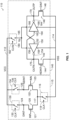
- FIG. 1 shows an example of a sense amplifier 110 according to certain aspects of the present disclosure.
- the sense amplifier 110 may be used, for example, in a data sampler to sample and resolve incoming data bits.
- the sense amplifier 110 includes an input circuit 115 and a regeneration circuit 140.
- the input circuit 115 may also be referred to as an input stage and the regeneration circuit 140 may also be referred to as a regeneration stage.
- the input circuit 115 includes a first input transistor 120, a second input transistor 122, a first switch 116, a second switch 130, and a third switch 134.
- the second switch 130 is coupled between a supply rail 112 and the first input transistor 120
- the third switch 134 is coupled between the supply rail 112 and the second input transistor 122.
- the first input transistor 120 is coupled between the second switch 130 and node 117
- the second input transistor 122 is coupled between the third switch 134 and node 117.
- the first switch 116 is coupled between node 117 and a ground 114.
- the first input transistor 120 is implemented with a first n-type field effect transistor (NFET) and the second input transistor 122 is implemented with a second NFET.
- the second switch 130 is coupled between the supply rail 112 and the drain of the first input transistor 120
- the first switch 116 is coupled between the source of the first input transistor 120 and the ground 114.
- the third switch 134 is coupled between the supply rail 112 and the drain of the second input transistor 122
- the first switch 116 is coupled between the source of the second input transistor 122 and the ground 114. It is to be appreciated that the first input transistor 120 and the second input transistor 122 are not limited to NFETs and may be implemented with other types of transistors.
- the input circuit 115 is configured to receive a differential input signal (e.g., differential data signal) that includes a first input voltage (labeled "INP") and a second input voltage (labeled "INN").
- the first input voltage INP is input to a first input 121 of the input circuit 115 and the second input voltage INN is input to a second input 123 of the input circuit 115, in which the first input 121 is coupled to the gate of the first input transistor 120 and the second input 123 is coupled to the gate of the second input transistor 122.
- the differential input signal may have a small differential voltage (i.e., a small difference between the first input voltage INP and the second input voltage INN) in which the polarity of the differential voltage represents a bit value.
- the sense amplifier 110 is configured to convert the small differential input voltage into a large differential output voltage to resolve the bit value.
- the first switch 116 has a control input 118 driven by a first timing signal
- the second switch 130 has a control input 132 driven by the first timing signal
- the third switch 134 has a control input 136 driven by the first timing signal.
- the first switch 116 is configured to turn on when the first timing signal is high and turn off when the first timing signal is low
- each one of the second switch 130 and the third switch 134 is configured to turn on when the first timing signal is low and turn off when the first timing signal is high.
- the first timing signal is a clock signal (labeled "CLK").
- CLK clock signal
- a "clock signal” is a periodic signal that oscillates between a high logic state and a low logic state.
- a high logic state i.e., logic state of one
- a low logic state i.e., logic state of zero
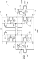
- the first input 1072 of the latch 1070 is coupled to the first output 170 and hence the drain of the second input transistor 146, and the second input 1074 of the latch 1070 is coupled to the second output 175 and hence the drain of the first input transistor 142.
- the present disclosure is not limited to this example.
- the first input 1072 of the latch 1070 may be coupled to the output 164 of the second inverting circuit 160, and the second input 1074 of the latch 1070 may be coupled to the output 154 of the first inverting circuit 150.
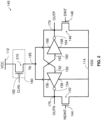
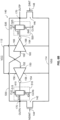
- the output of the first inverting circuit is decoupled from the first transistor.
- the output of the first inverting circuit may be decoupled from the first transistor by turning off the first switch 510.
- the output of the second inverting circuit is decoupled from the second transistor.
- the output of the second inverting circuit may be decoupled from the second transistor by turning off the second switch 520.
- the output of the first inverting circuit is coupled to the first transistor.
- the output of the first inverting circuit may be coupled to the first transistor by turning on the first switch 510.
- the method 1100 may also include driving a gate of the first transistor with a first input signal (e.g., voltage NDINT) and driving a gate of the second transistor with a second input signal (e.g., voltage DINT).
- the first input signal and the second input signal may be generated by the input circuit 115 based on a data signal (e.g., a differential data signal) input to the input circuit 115.
- the first input signal is above a threshold voltage of the first transistor
- the second input signal is above a threshold voltage of the second transistor.
- the threshold voltage of the first transistor may be approximately the same as the threshold voltage of the second transistor.
- the first input signal is above the threshold voltage of the first transistor, and the second input signal is above the threshold voltage of the second transistor.
- the first input signal e.g., voltage NDINT
- the second input signal e.g., voltage DINT
- the first rate and the second rate are different (e.g., based on the polarity of the data signal input to the input circuit 115).
- the method 1100 may also include transitioning from the sensing phase to a decision phase when the first input signal falls below the threshold voltage of the first transistor or the second input signal falls below the threshold voltage of the second transistor.
- the method 1100 may also include, in the decision phase, resolving a bit value based on the first input signal and the second input signal.
- resolving the bit value may include resolving to a first bit value if the first input signal falls below the threshold voltage of the first transistor before the second input signal falls below the threshold voltage of the second transistor, and resolving to a second bit value if the second input signal falls below the threshold voltage of the second transistor before the first input signal falls below the threshold voltage of the first transistor.
- the first bit value may be a one and the second bit value may be a zero, or vice versa.
- the output of the first inverting circuit is coupled to the first transistor and the output of the second inverting circuit is coupled to the second transistor, which cross couples the first inverting circuit and the second inverting circuit. This is because the first transistor is coupled to the input of the second inverting circuit and the second transistor is coupled to the input of the first inverting circuit.
- the cross coupling of the first inverting circuit and the second inverting circuit provides regenerative feedback, which facilitates resolving the bit value.
- the input circuit 115 may also be referred to as a sensing circuit or another term.
- the regeneration circuit 140 may also be referred to as a decision circuit, a cross-coupled latch, or another term.
- An inverting circuit may also be referred to as an inverter, or another term.
- a logic state may also be referred to as a logic level, a logic value, or another term.
- any reference to an element herein using a designation such as "first,” “second,” and so forth does not generally limit the quantity or order of those elements. Rather, these designations are used herein as a convenient way of distinguishing between two or more elements or instances of an element. Thus, a reference to first and second elements does not mean that only two elements can be employed, or that the first element must precede the second element.
- the word "exemplary” is used to mean “serving as an example, instance, or illustration.” Any implementation or aspect described herein as “exemplary” is not necessarily to be construed as preferred or advantageous over other aspects of the disclosure. Likewise, the term “aspects” does not require that all aspects of the disclosure include the discussed feature, advantage or mode of operation. The term “approximately”, as used herein with respect to a stated value or a property, is intended to indicate being within 10% of the stated value or property.
Landscapes
- Physics & Mathematics (AREA)
- Nonlinear Science (AREA)
- Engineering & Computer Science (AREA)
- Theoretical Computer Science (AREA)
- Amplifiers (AREA)
- Dram (AREA)
- Logic Circuits (AREA)
- Static Random-Access Memory (AREA)
- Manipulation Of Pulses (AREA)
Claims (15)
- Eine Regenerierungsschaltung (140) für einen Leseverstärker, aufweisend:eine erste Inverterschaltung (150), die einen Eingang (152) und einen Ausgang (154) aufweist,eine zweite Inverterschaltung (160), die einen Eingang (162) und einen Ausgang (164) aufweist,einen ersten Transistor (142), der mit dem Eingang der zweiten Inverterschaltung über einen ersten Knoten (175) gekoppelt ist, wobei ein Gate (144) des ersten Transistors konfiguriert ist zum Empfangen eines ersten Eingangssignals (NDINT),einen zweiten Transistor (146), der mit dem Eingang der ersten Inverterschaltung über einen zweiten Knoten (170) gekoppelt ist, wobei ein Gate (148) des zweiten Transistors konfiguriert ist zum Empfangen eines zweiten Eingangssignals (DINT),einen ersten Schalter (510), der zwischen dem ersten Transistor über den ersten Knoten und dem Ausgang der ersten Inverterschaltung gekoppelt ist, wobei ein Steuereingang (515) des ersten Schalters konfiguriert ist zum Empfangen eines Zeitsignals (CLK), und wobei der erste Schalter konfiguriert ist zum Entkoppeln des Ausgangs der ersten Inverterschaltung von dem Eingang der zweiten Inverterschaltung, wenn das Zeitsignal den ersten Schalter ausschaltet,einen zweiten Schalter (520), der zwischen dem zweiten Transistor über den zweiten Knoten und dem Ausgang der zweiten Inverterschaltung gekoppelt ist, wobei ein Steuereingang (525) des zweiten Schalters konfiguriert ist zum Empfangen des Zeitsignals, und wobei der zweite Schalter konfiguriert ist zum Entkoppeln des Ausgangs der zweiten Inverterschaltung von dem Eingang der ersten Inverterschaltung, wenn das Zeitsignal den zweiten Schalter ausschaltet.
- Regenerierungsschaltung nach Anspruch 1, wobei:der erste Schalter zwischen einem Drain des ersten Transistors und dem Ausgang der ersten Inverterschaltung gekoppelt ist, undder zweite Schalter zwischen einem Drain des zweiten Transistors und dem Ausgang der zweiten Inverterschaltung gekoppelt ist
- Regenerierungsschaltung nach Anspruch 2, wobei:eine Source des ersten Transistors mit einer Erde (114, VSS) gekoppelt ist,eine Source des zweiten Transistors mit der Erde gekoppelt ist,der erste Transistor ein erster n-Typ-Feldeffekttransistor (NFET) ist und der zweite Transistor ein zweiter NFET ist,der Drain des ersten Transistors direkt mit dem Eingang der zweiten Inverterschaltung gekoppelt ist, undder Drain des zweiten Transistors direkt mit dem Eingang der ersten Inverterschaltung gekoppelt ist.
- Regenerierungsschaltung nach Anspruch 1, wobeider erste Schalter einen dritten Transistor (610) mit einem Gate, das konfiguriert ist zum Empfangen des Zeitsignals, umfasst,der zweite Schalter einen vierten Transistor (620) mit einem Gate, das konfiguriert ist zum Empfangen des Zeitsignals, umfasst,eine Source oder ein Drain des dritten Transistors mit einem Drain des ersten Transistors gekoppelt ist und entsprechend das Drain oder die Source des dritten Transistors mit dem Ausgang der ersten Inverterschaltung gekoppelt ist,eine Source oder ein Drain des vierten Transistors mit einem Drain des zweiten Transistors gekoppelt ist und entsprechend das Drain oder die Source des vierten Transistors mit dem Ausgang der zweiten Inverterschaltung gekoppelt ist,der dritte Transistor ein erster n-Typ-Feldeffekttransistor (NFET) ist, undder vierte Transistor ein zweiter NFET ist.
- Regenerierungsschaltung nach Anspruch 1, wobei:die zweite Inverterschaltung einen dritten Transistor (755) umfasst, der zwischen dem Eingang der ersten Inverterschaltung über den zweiten Schalter und einer Versorgungsschiene (112, VCC) gekoppelt ist, unddie erste Inverterschaltung einen vierten Transistor (745) umfasst, der zwischen dem Eingang der zweiten Inverterschaltung über den zweiten Schalter und der Versorgungsschiene gekoppelt ist,ein Gate (737) des dritten Transistors mit dem Ausgang der ersten Inverterschaltung über den ersten Schalter gekoppelt ist,ein Gate (727) des vierten Transistors mit dem Ausgang der zweiten Inverterschaltung über den zweiten Schalter gekoppelt ist,eine Source des dritten Transistors mit der Versorgungsschiene gekoppelt ist und ein Drain des dritten Transistors mit dem Eingang der ersten Inverterschaltung gekoppelt ist,eine Source des vierten Transistors mit der Versorgungsschiene gekoppelt ist und ein Drain des vierten Transistors mit dem Eingang der zweiten Inverterschaltung gekoppelt ist,der dritte Transistor ein erster p-Typ-Feldeffekttransistor (PFET) ist, undder vierte Transistor ein zweiter PFET ist.
- Regenerierungsschaltung nach Anspruch 1, wobei das Zeitsignal ein Taktsignal ist.
- Regenerierungsschaltung nach Anspruch 1, wobei der Steuereingang des ersten Schalters und der Steuereingang des zweiten Schalters mit einer Zeitsignalschaltung, die konfiguriert ist zum Generieren des Zeitsignals, gekoppelt sind.
- Ein Leseverstärker (110), aufweisend:eine Eingangsschaltung (115), wobei die Eingangsschaltung aufweist:einen ersten Eingangsschaltung-Transistor (120), wobei ein Gate (121) des ersten Transistors konfiguriert ist zum Empfangen eines ersten Eingangssignals (INP) und ein Drain des ersten Transistors mit einem ersten Ausgang (124, DINT) der Eingangsschaltung gekoppelt ist, undeinen zweiten Eingangsschaltung-Transistor (122), wobei ein Gate (123) des zweiten Transistors konfiguriert ist zum Empfangen eines zweiten Eingangssignals (INN) und ein Drain des zweiten Transistors mit einem zweiten Ausgang (126, NDINT) der Eingangsschaltung gekoppelt ist, unddie Regenerierungsschaltung eines der Ansprüche 1-7, wobei:das Gate des ersten Transistors mit dem zweiten Ausgang der Eingangsschaltung gekoppelt ist, unddas Gate des zweiten Transistors mit dem ersten Ausgang der Eingangsschaltung gekoppelt ist.
- Leseverstärker nach Anspruch 8, wobei die Eingangsschaltung weiterhin aufweist:einen ersten Eingangsschaltung-Schalter (130), der zwischen dem Drain des ersten Transistors und einer Versorgungsschiene (VCC) gekoppelt ist, undeinen zweiten Eingangsschaltung-Schalter (134), der zwischen dem Drain des zweiten Transistors und der Versorgungsschiene gekoppelt ist.
- Leseverstärker nach Anspruch 9, wobei:ein Steuereingang (132) des ersten Eingangsschaltung-Schalters konfiguriert ist zum Empfangen des Zeitsignals, undein Steuereingang (136) des zweiten Eingangsschaltung-Schalters konfiguriert ist zum Empfangen des Zeitsignals.
- Leseverstärker nach Anspruch 9, wobei die Eingangsschaltung weiterhin einen dritten Eingangsschaltung-Schalter (116) umfasst, der zwischen einer Source des ersten Transistors und einer Erde (VSS) gekoppelt ist und zwischen einer Source des zweiten Transistors und der Erde gekoppelt ist,
wobei:ein Steuereingang (132) des ersten Eingangsschaltung-Schalters konfiguriert ist zum Empfangen des Zeitsignals,ein Steuereingang (136) des zweiten Eingangsschaltung-Schalters konfiguriert ist zum Empfangen des Zeitsignals, undein Steuereingang (118) des dritten Eingangsschaltung-Schalters konfiguriert ist zum Empfangen des Zeitsignals. - Ein Verfahren (1100) zum Betreiben der Regenerierungsschaltung gemäß einem der Ansprüche 1-7, aufweisend:Treiben des Gates des ersten Transistors mit dem ersten Eingangssignal,Treiben des Gates des zweiten Transistors mit dem zweiten Eingangssignal,in einer Rücksetzphase:Entkoppeln (1110), über den ersten Schalter, des Ausgangs der ersten Inverterschaltung von dem ersten Transistor und dem Eingang der zweiten Inverterschaltung, undEntkoppeln (1120), über den zweiten Schalter, des Ausgangs der zweiten Inverterschaltung von dem zweiten Transistor und dem Eingang der ersten Inverterschaltung, undin einer Lesephase:Koppeln (1130), über den ersten Schalter, des Ausgangs der ersten Inverterschaltung mit dem ersten Transistor und dem Eingang der zweiten Inverterschaltung, undKoppeln (1140), über den zweiten Schalter, des Ausgangs der zweiten Inverterschaltung mit dem zweiten Transistor und dem Eingang der ersten Inverterschaltung.
- Verfahren nach Anspruch 12, wobei:in der Rücksetzphase das erste Eingangssignal über einer Schwellenspannung des ersten Transistors ist und das zweite Eingangssignal über einer Schwellenspannung des zweiten Transistors ist,in der Lesephase das erste Eingangssignal über der Schwellenspannung des ersten Transistors ist und das zweite Eingangssignal über der Schwellenspannung des zweiten Transistors ist,in der Lesephase das erste Eingangssignal mit einer ersten Rate fällt und das zweite Eingangssignal mit einer zweiten Rate fällt, wobei die erste Rate und die zweite Rate verschieden sind,von der Lesephase zu einer Entscheidungsphase übergegangen wird, wenn das erste Eingangssignal unter die Schwellenspannung des ersten Transistors fällt oder das zweite Eingangssignal unter die Schwellenspannung des zweiten Transistors fällt, undin der Entscheidungsphase ein Bitwert basierend auf dem ersten Eingangssignal und dem zweiten Eingangssignal aufgelöst wird.
- Verfahren nach Anspruch 12, wobei:das Entkoppeln des Ausgangs der ersten Inverterschaltung von dem ersten Transistor das Ausschalten des ersten Schalters aufweist,das Entkoppeln des Ausgangs der zweiten Inverterschaltung von dem zweiten Transistor das Ausschalten des zweiten Schalters aufweist,das Koppeln des Ausgangs der ersten Inverterschaltung mit dem ersten Transistor das Einschalten des ersten Schalters aufweist, unddas Koppeln des Ausgangs der zweiten Inverterschaltung mit dem zweiten Transistor das Einschalten des zweiten Schalters aufweist.
- Verfahren nach Anspruch 12, wobei ein Drain des ersten Transistors direkt mit dem Eingang der zweiten Inverterschaltung gekoppelt ist und ein Drain des zweiten Transistors direkt mit dem Eingang der ersten Inverterschaltung gekoppelt ist,
wobei:das Entkoppeln des Ausgangs der ersten Inverterschaltung von dem ersten Transistor das Entkoppeln des Ausgangs der ersten Inverterschaltung von dem Drain des ersten Transistors aufweist,das Entkoppeln des Ausgangs der zweiten Inverterschaltung von dem zweiten Transistor das Entkoppeln des Ausgangs der zweiten Inverterschaltung von dem Drain des zweiten Transistors aufweist,das Koppeln des Ausgangs der ersten Inverterschaltung mit dem Transistor das Koppeln des Ausgangs der ersten Inverterschaltung mit dem Drain des ersten Transistors aufweist,das Koppeln des Ausgangs der zweiten Inverterschaltung mit dem zweiten Transistor das Koppeln des Ausgangs der zweiten Inverterschaltung mit dem Drain des zweiten Transistors aufweist,wobei weiterhin in der Regenerierungsschaltung der erste Schalter zwischen dem Ausgang der ersten Inverterschaltung und dem Drain des ersten Transistors gekoppelt ist und der zweite Schalter zwischen dem Ausgang der zweiten Inverterschaltung und dem Drain des zweiten Transistors gekoppelt ist, wobei:das Entkoppeln des Ausgangs der ersten Inverterschaltung von dem Drain des ersten Transistors das Ausschalten des ersten Schalters aufweist,das Entkoppeln des Ausgangs der zweiten Inverterschaltung von dem Drain des zweiten Transistors das Ausschalten des zweiten Schalters aufweist,das Koppeln des Ausgangs der ersten Inverterschaltung mit dem Drain des ersten Transistors das Einschalten des ersten Schalters aufweist, unddas Koppeln des Ausgangs der zweiten Inverterschaltung mit dem Drain des zweiten Transistors das Einschalten des zweiten Schalters aufweist.
Applications Claiming Priority (2)
| Application Number | Priority Date | Filing Date | Title |
|---|---|---|---|
| US17/321,005 US11374560B1 (en) | 2021-05-14 | 2021-05-14 | Dynamic cross-coupled regeneration for high-speed sense amplifier |
| PCT/US2022/026719 WO2022240591A1 (en) | 2021-05-14 | 2022-04-28 | Dynamic cross-coupled regeneration for high-speed sense amplifier |
Publications (4)
| Publication Number | Publication Date |
|---|---|
| EP4338158A1 EP4338158A1 (de) | 2024-03-20 |
| EP4338158C0 EP4338158C0 (de) | 2025-03-19 |
| EP4338158B1 true EP4338158B1 (de) | 2025-03-19 |
| EP4338158B9 EP4338158B9 (de) | 2025-08-06 |
Family
ID=81655005
Family Applications (1)
| Application Number | Title | Priority Date | Filing Date |
|---|---|---|---|
| EP22723917.5A Active EP4338158B9 (de) | 2021-05-14 | 2022-04-28 | Dynamische kreuzgekoppelte regeneration für einen schnellen leseverstärker |
Country Status (7)
| Country | Link |
|---|---|
| US (1) | US11374560B1 (de) |
| EP (1) | EP4338158B9 (de) |
| KR (1) | KR102618435B1 (de) |
| CN (1) | CN117378008A (de) |
| BR (1) | BR112023023040A2 (de) |
| TW (1) | TWI910346B (de) |
| WO (1) | WO2022240591A1 (de) |
Families Citing this family (1)
| Publication number | Priority date | Publication date | Assignee | Title |
|---|---|---|---|---|
| US11711077B1 (en) * | 2022-06-02 | 2023-07-25 | Qualcomm Incorporated | High-speed sampler |
Family Cites Families (20)
| Publication number | Priority date | Publication date | Assignee | Title |
|---|---|---|---|---|
| US5508648A (en) * | 1994-08-01 | 1996-04-16 | Intel Corporation | Differential latch circuit |
| US6396308B1 (en) | 2001-02-27 | 2002-05-28 | Sun Microsystems, Inc. | Sense amplifier with dual linearly weighted inputs and offset voltage correction |
| KR100394573B1 (ko) | 2001-05-31 | 2003-08-14 | 삼성전자주식회사 | 반도체 메모리장치의 센스앰프회로 |
| US7227798B2 (en) | 2002-10-07 | 2007-06-05 | Stmicroelectronics Pvt. Ltd. | Latch-type sense amplifier |
| US7196550B1 (en) * | 2003-06-26 | 2007-03-27 | Cypress Semiconductor Corporation | Complementary CMOS driver circuit with de-skew control |
| DE602005020457D1 (de) * | 2004-08-10 | 2010-05-20 | Nippon Telegraph & Telephone | Master-slave-flip-flop, trigger-flip-flop und zähler |
| JP4467445B2 (ja) * | 2005-02-10 | 2010-05-26 | Okiセミコンダクタ株式会社 | コンパレータ回路 |
| US7388772B1 (en) * | 2006-03-20 | 2008-06-17 | Altera Corporation | Latch circuit |
| US7679405B2 (en) * | 2007-10-24 | 2010-03-16 | Agere Systems Inc. | Latch-based sense amplifier |
| KR101063872B1 (ko) | 2009-05-07 | 2011-09-15 | 포항공과대학교 산학협력단 | 아날로그 디지털 변환기용 저전력 저역입력 잡음 비교기 회로 |
| US8604838B2 (en) * | 2011-12-12 | 2013-12-10 | Texas Instruments Incorporated | Comparator with improved time constant |
| US8624632B2 (en) | 2012-03-29 | 2014-01-07 | International Business Machines Corporation | Sense amplifier-type latch circuits with static bias current for enhanced operating frequency |
| US9467133B2 (en) * | 2015-02-27 | 2016-10-11 | Huawei Technologies Co., Ltd. | Comparator apparatus and method |
| US10230361B2 (en) * | 2015-08-28 | 2019-03-12 | Perceptia Devices Australia Pty Ltd | High-speed clocked comparators |
| JP2017112537A (ja) * | 2015-12-17 | 2017-06-22 | シナプティクス・ジャパン合同会社 | インバータ回路 |
| KR101880491B1 (ko) * | 2017-04-14 | 2018-07-20 | 광주과학기술원 | 저전력 시간 증폭기 및 그의 동작 방법 |
| KR102319827B1 (ko) | 2017-06-28 | 2021-11-01 | 에스케이하이닉스 주식회사 | 증폭기 회로 |
| KR102643532B1 (ko) * | 2018-08-28 | 2024-03-06 | 에스케이하이닉스 주식회사 | 비트라인 센스앰프 회로 |
| EP3672077B1 (de) | 2018-12-19 | 2022-07-27 | Socionext Inc. | Komparatorschaltung |
| US11095273B1 (en) * | 2020-07-27 | 2021-08-17 | Qualcomm Incorporated | High-speed sense amplifier with a dynamically cross-coupled regeneration stage |
-
2021
- 2021-05-14 US US17/321,005 patent/US11374560B1/en active Active
-
2022
- 2022-04-28 CN CN202280032104.3A patent/CN117378008A/zh active Pending
- 2022-04-28 KR KR1020237038338A patent/KR102618435B1/ko active Active
- 2022-04-28 EP EP22723917.5A patent/EP4338158B9/de active Active
- 2022-04-28 WO PCT/US2022/026719 patent/WO2022240591A1/en not_active Ceased
- 2022-04-28 BR BR112023023040A patent/BR112023023040A2/pt unknown
- 2022-04-28 TW TW111116285A patent/TWI910346B/zh active
Also Published As
| Publication number | Publication date |
|---|---|
| CN117378008A (zh) | 2024-01-09 |
| BR112023023040A2 (pt) | 2024-01-23 |
| TWI910346B (zh) | 2026-01-01 |
| US11374560B1 (en) | 2022-06-28 |
| KR102618435B1 (ko) | 2023-12-27 |
| KR20230160405A (ko) | 2023-11-23 |
| EP4338158C0 (de) | 2025-03-19 |
| TW202304137A (zh) | 2023-01-16 |
| EP4338158A1 (de) | 2024-03-20 |
| WO2022240591A1 (en) | 2022-11-17 |
| EP4338158B9 (de) | 2025-08-06 |
Similar Documents
| Publication | Publication Date | Title |
|---|---|---|
| EP4189683B1 (de) | Hochgeschwindigkeitsleseverstärker mit einer dynamisch kreuzgekoppelten regenerationsstufe | |
| US7135889B2 (en) | Universal single-ended parallel bus | |
| EP4338158B9 (de) | Dynamische kreuzgekoppelte regeneration für einen schnellen leseverstärker | |
| US7259592B2 (en) | Output drivers having adjustable swing widths during test mode operation | |
| US6441649B1 (en) | Rail-to-rail input clocked amplifier | |
| JP2025157269A (ja) | 高速サンプラ | |
| US7388406B2 (en) | CML circuit devices having improved headroom | |
| US6281714B1 (en) | Differential receiver | |
| US12143106B2 (en) | Semiconductor device including a level shifter and method of mitigating a delay between input and output signals | |
| US6411131B1 (en) | Method for differentiating a differential voltage signal using current based differentiation | |
| KR20000043230A (ko) | 데이타 입력버퍼 | |
| BR112023000474B1 (pt) | Estágio de regeneração de um amplificador de detecção e método de operação de um estágio de regeneração de um amplificador de detecção |
Legal Events
| Date | Code | Title | Description |
|---|---|---|---|
| STAA | Information on the status of an ep patent application or granted ep patent |
Free format text: STATUS: UNKNOWN |
|
| STAA | Information on the status of an ep patent application or granted ep patent |
Free format text: STATUS: THE INTERNATIONAL PUBLICATION HAS BEEN MADE |
|
| PUAI | Public reference made under article 153(3) epc to a published international application that has entered the european phase |
Free format text: ORIGINAL CODE: 0009012 |
|
| STAA | Information on the status of an ep patent application or granted ep patent |
Free format text: STATUS: REQUEST FOR EXAMINATION WAS MADE |
|
| 17P | Request for examination filed |
Effective date: 20230921 |
|
| AK | Designated contracting states |
Kind code of ref document: A1 Designated state(s): AL AT BE BG CH CY CZ DE DK EE ES FI FR GB GR HR HU IE IS IT LI LT LU LV MC MK MT NL NO PL PT RO RS SE SI SK SM TR |
|
| DAV | Request for validation of the european patent (deleted) | ||
| DAX | Request for extension of the european patent (deleted) | ||
| GRAP | Despatch of communication of intention to grant a patent |
Free format text: ORIGINAL CODE: EPIDOSNIGR1 |
|
| STAA | Information on the status of an ep patent application or granted ep patent |
Free format text: STATUS: GRANT OF PATENT IS INTENDED |
|
| RIC1 | Information provided on ipc code assigned before grant |
Ipc: H03M 9/00 20060101ALN20240923BHEP Ipc: H03K 5/24 20060101ALN20240923BHEP Ipc: G11C 7/10 20060101ALN20240923BHEP Ipc: G11C 7/08 20060101ALI20240923BHEP Ipc: G11C 7/06 20060101AFI20240923BHEP |
|
| INTG | Intention to grant announced |
Effective date: 20241022 |
|
| GRAS | Grant fee paid |
Free format text: ORIGINAL CODE: EPIDOSNIGR3 |
|
| GRAA | (expected) grant |
Free format text: ORIGINAL CODE: 0009210 |
|
| STAA | Information on the status of an ep patent application or granted ep patent |
Free format text: STATUS: THE PATENT HAS BEEN GRANTED |
|
| AK | Designated contracting states |
Kind code of ref document: B1 Designated state(s): AL AT BE BG CH CY CZ DE DK EE ES FI FR GB GR HR HU IE IS IT LI LT LU LV MC MK MT NL NO PL PT RO RS SE SI SK SM TR |
|
| REG | Reference to a national code |
Ref country code: GB Ref legal event code: FG4D |
|
| REG | Reference to a national code |
Ref country code: CH Ref legal event code: EP |
|
| REG | Reference to a national code |
Ref country code: DE Ref legal event code: R096 Ref document number: 602022012009 Country of ref document: DE |
|
| REG | Reference to a national code |
Ref country code: IE Ref legal event code: FG4D |
|
| U01 | Request for unitary effect filed |
Effective date: 20250402 |
|
| U07 | Unitary effect registered |
Designated state(s): AT BE BG DE DK EE FI FR IT LT LU LV MT NL PT RO SE SI Effective date: 20250410 |
|
| PG25 | Lapsed in a contracting state [announced via postgrant information from national office to epo] |
Ref country code: RS Free format text: LAPSE BECAUSE OF FAILURE TO SUBMIT A TRANSLATION OF THE DESCRIPTION OR TO PAY THE FEE WITHIN THE PRESCRIBED TIME-LIMIT Effective date: 20250619 |
|
| PG25 | Lapsed in a contracting state [announced via postgrant information from national office to epo] |
Ref country code: NO Free format text: LAPSE BECAUSE OF FAILURE TO SUBMIT A TRANSLATION OF THE DESCRIPTION OR TO PAY THE FEE WITHIN THE PRESCRIBED TIME-LIMIT Effective date: 20250619 |
|
| REG | Reference to a national code |
Ref country code: CH Ref legal event code: PK Free format text: BERICHTIGUNG B9 |
|
| PG25 | Lapsed in a contracting state [announced via postgrant information from national office to epo] |
Ref country code: HR Free format text: LAPSE BECAUSE OF FAILURE TO SUBMIT A TRANSLATION OF THE DESCRIPTION OR TO PAY THE FEE WITHIN THE PRESCRIBED TIME-LIMIT Effective date: 20250319 |
|
| PG25 | Lapsed in a contracting state [announced via postgrant information from national office to epo] |
Ref country code: GR Free format text: LAPSE BECAUSE OF FAILURE TO SUBMIT A TRANSLATION OF THE DESCRIPTION OR TO PAY THE FEE WITHIN THE PRESCRIBED TIME-LIMIT Effective date: 20250620 |
|
| PG25 | Lapsed in a contracting state [announced via postgrant information from national office to epo] |
Ref country code: SM Free format text: LAPSE BECAUSE OF FAILURE TO SUBMIT A TRANSLATION OF THE DESCRIPTION OR TO PAY THE FEE WITHIN THE PRESCRIBED TIME-LIMIT Effective date: 20250319 |
|
| PG25 | Lapsed in a contracting state [announced via postgrant information from national office to epo] |
Ref country code: ES Free format text: LAPSE BECAUSE OF FAILURE TO SUBMIT A TRANSLATION OF THE DESCRIPTION OR TO PAY THE FEE WITHIN THE PRESCRIBED TIME-LIMIT Effective date: 20250319 |
|
| PG25 | Lapsed in a contracting state [announced via postgrant information from national office to epo] |
Ref country code: PL Free format text: LAPSE BECAUSE OF FAILURE TO SUBMIT A TRANSLATION OF THE DESCRIPTION OR TO PAY THE FEE WITHIN THE PRESCRIBED TIME-LIMIT Effective date: 20250319 |
|
| PG25 | Lapsed in a contracting state [announced via postgrant information from national office to epo] |
Ref country code: CZ Free format text: LAPSE BECAUSE OF FAILURE TO SUBMIT A TRANSLATION OF THE DESCRIPTION OR TO PAY THE FEE WITHIN THE PRESCRIBED TIME-LIMIT Effective date: 20250319 |
|
| PG25 | Lapsed in a contracting state [announced via postgrant information from national office to epo] |
Ref country code: SK Free format text: LAPSE BECAUSE OF FAILURE TO SUBMIT A TRANSLATION OF THE DESCRIPTION OR TO PAY THE FEE WITHIN THE PRESCRIBED TIME-LIMIT Effective date: 20250319 |
|
| PG25 | Lapsed in a contracting state [announced via postgrant information from national office to epo] |
Ref country code: IS Free format text: LAPSE BECAUSE OF FAILURE TO SUBMIT A TRANSLATION OF THE DESCRIPTION OR TO PAY THE FEE WITHIN THE PRESCRIBED TIME-LIMIT Effective date: 20250719 |
|
| U21 | Renewal fee for the european patent with unitary effect paid with additional fee |
Year of fee payment: 4 Effective date: 20251008 |
|
| REG | Reference to a national code |
Ref country code: CH Ref legal event code: H13 Free format text: ST27 STATUS EVENT CODE: U-0-0-H10-H13 (AS PROVIDED BY THE NATIONAL OFFICE) Effective date: 20251125 |
|
| PG25 | Lapsed in a contracting state [announced via postgrant information from national office to epo] |
Ref country code: MC Free format text: LAPSE BECAUSE OF FAILURE TO SUBMIT A TRANSLATION OF THE DESCRIPTION OR TO PAY THE FEE WITHIN THE PRESCRIBED TIME-LIMIT Effective date: 20250319 |
|
| PG25 | Lapsed in a contracting state [announced via postgrant information from national office to epo] |
Ref country code: CH Free format text: LAPSE BECAUSE OF NON-PAYMENT OF DUE FEES Effective date: 20250430 |
|
| PLBE | No opposition filed within time limit |
Free format text: ORIGINAL CODE: 0009261 |
|
| STAA | Information on the status of an ep patent application or granted ep patent |
Free format text: STATUS: NO OPPOSITION FILED WITHIN TIME LIMIT |
|
| REG | Reference to a national code |
Ref country code: CH Ref legal event code: L10 Free format text: ST27 STATUS EVENT CODE: U-0-0-L10-L00 (AS PROVIDED BY THE NATIONAL OFFICE) Effective date: 20260128 |
|
| 26N | No opposition filed |
Effective date: 20251222 |
|
| PGFP | Annual fee paid to national office [announced via postgrant information from national office to epo] |
Ref country code: GB Payment date: 20260320 Year of fee payment: 5 |
|
| PGFP | Annual fee paid to national office [announced via postgrant information from national office to epo] |
Ref country code: IE Payment date: 20260317 Year of fee payment: 5 |
|
| U20 | Renewal fee for the european patent with unitary effect paid |
Year of fee payment: 5 Effective date: 20260320 |