EP4333003A2 - Mehrschichtiges elektronisches bauteil - Google Patents
Mehrschichtiges elektronisches bauteil Download PDFInfo
- Publication number
- EP4333003A2 EP4333003A2 EP23186353.1A EP23186353A EP4333003A2 EP 4333003 A2 EP4333003 A2 EP 4333003A2 EP 23186353 A EP23186353 A EP 23186353A EP 4333003 A2 EP4333003 A2 EP 4333003A2
- Authority
- EP
- European Patent Office
- Prior art keywords
- electrode layer
- disposed
- layer
- corner
- intermediate electrode
- Prior art date
- Legal status (The legal status is an assumption and is not a legal conclusion. Google has not performed a legal analysis and makes no representation as to the accuracy of the status listed.)
- Pending
Links
- 239000011347 resin Substances 0.000 claims abstract description 83
- 229920005989 resin Polymers 0.000 claims abstract description 83
- 238000007747 plating Methods 0.000 claims abstract description 64
- 229910052751 metal Inorganic materials 0.000 claims description 16
- 239000002184 metal Substances 0.000 claims description 16
- 230000015572 biosynthetic process Effects 0.000 claims description 11
- 239000011521 glass Substances 0.000 claims description 10
- 230000002093 peripheral effect Effects 0.000 claims description 5
- PXHVJJICTQNCMI-UHFFFAOYSA-N Nickel Chemical compound [Ni] PXHVJJICTQNCMI-UHFFFAOYSA-N 0.000 description 15
- 238000000034 method Methods 0.000 description 15
- 238000012360 testing method Methods 0.000 description 13
- 238000005245 sintering Methods 0.000 description 9
- 239000011135 tin Substances 0.000 description 9
- 239000000919 ceramic Substances 0.000 description 8
- 239000003985 ceramic capacitor Substances 0.000 description 8
- 230000035515 penetration Effects 0.000 description 8
- KDLHZDBZIXYQEI-UHFFFAOYSA-N Palladium Chemical compound [Pd] KDLHZDBZIXYQEI-UHFFFAOYSA-N 0.000 description 6
- 239000011342 resin composition Substances 0.000 description 6
- 229910045601 alloy Inorganic materials 0.000 description 5
- 239000000956 alloy Substances 0.000 description 5
- 239000010949 copper Substances 0.000 description 5
- 229910052759 nickel Inorganic materials 0.000 description 5
- 229910052718 tin Inorganic materials 0.000 description 5
- 239000011248 coating agent Substances 0.000 description 4
- 238000000576 coating method Methods 0.000 description 4
- 229910052802 copper Inorganic materials 0.000 description 4
- 230000007547 defect Effects 0.000 description 4
- 238000011156 evaluation Methods 0.000 description 4
- 229910052763 palladium Inorganic materials 0.000 description 4
- 239000002245 particle Substances 0.000 description 4
- 239000000843 powder Substances 0.000 description 4
- 230000008901 benefit Effects 0.000 description 3
- 229910052804 chromium Inorganic materials 0.000 description 3
- 239000011651 chromium Substances 0.000 description 3
- 238000005336 cracking Methods 0.000 description 3
- BASFCYQUMIYNBI-UHFFFAOYSA-N platinum Chemical compound [Pt] BASFCYQUMIYNBI-UHFFFAOYSA-N 0.000 description 3
- 230000035939 shock Effects 0.000 description 3
- 239000012798 spherical particle Substances 0.000 description 3
- 229910002113 barium titanate Inorganic materials 0.000 description 2
- 238000005452 bending Methods 0.000 description 2
- 230000007423 decrease Effects 0.000 description 2
- 230000002950 deficient Effects 0.000 description 2
- 238000007598 dipping method Methods 0.000 description 2
- 230000014509 gene expression Effects 0.000 description 2
- 239000010931 gold Substances 0.000 description 2
- 238000005259 measurement Methods 0.000 description 2
- 238000012986 modification Methods 0.000 description 2
- 230000004048 modification Effects 0.000 description 2
- 230000000149 penetrating effect Effects 0.000 description 2
- 230000005855 radiation Effects 0.000 description 2
- 229910052709 silver Inorganic materials 0.000 description 2
- 239000002002 slurry Substances 0.000 description 2
- 239000000126 substance Substances 0.000 description 2
- 239000010936 titanium Substances 0.000 description 2
- 239000004925 Acrylic resin Substances 0.000 description 1
- 229920000178 Acrylic resin Polymers 0.000 description 1
- RYGMFSIKBFXOCR-UHFFFAOYSA-N Copper Chemical compound [Cu] RYGMFSIKBFXOCR-UHFFFAOYSA-N 0.000 description 1
- 239000001856 Ethyl cellulose Substances 0.000 description 1
- ZZSNKZQZMQGXPY-UHFFFAOYSA-N Ethyl cellulose Chemical compound CCOCC1OC(OC)C(OCC)C(OCC)C1OC1C(O)C(O)C(OC)C(CO)O1 ZZSNKZQZMQGXPY-UHFFFAOYSA-N 0.000 description 1
- BQCADISMDOOEFD-UHFFFAOYSA-N Silver Chemical compound [Ag] BQCADISMDOOEFD-UHFFFAOYSA-N 0.000 description 1
- ATJFFYVFTNAWJD-UHFFFAOYSA-N Tin Chemical compound [Sn] ATJFFYVFTNAWJD-UHFFFAOYSA-N 0.000 description 1
- RTAQQCXQSZGOHL-UHFFFAOYSA-N Titanium Chemical compound [Ti] RTAQQCXQSZGOHL-UHFFFAOYSA-N 0.000 description 1
- JRPBQTZRNDNNOP-UHFFFAOYSA-N barium titanate Chemical compound [Ba+2].[Ba+2].[O-][Ti]([O-])([O-])[O-] JRPBQTZRNDNNOP-UHFFFAOYSA-N 0.000 description 1
- 239000011230 binding agent Substances 0.000 description 1
- 239000003990 capacitor Substances 0.000 description 1
- 230000008094 contradictory effect Effects 0.000 description 1
- 238000009792 diffusion process Methods 0.000 description 1
- 238000001035 drying Methods 0.000 description 1
- 230000000694 effects Effects 0.000 description 1
- 230000005611 electricity Effects 0.000 description 1
- 238000007772 electroless plating Methods 0.000 description 1
- 238000009713 electroplating Methods 0.000 description 1
- 239000003822 epoxy resin Substances 0.000 description 1
- 229920001249 ethyl cellulose Polymers 0.000 description 1
- 235000019325 ethyl cellulose Nutrition 0.000 description 1
- PCHJSUWPFVWCPO-UHFFFAOYSA-N gold Chemical compound [Au] PCHJSUWPFVWCPO-UHFFFAOYSA-N 0.000 description 1
- 229910052737 gold Inorganic materials 0.000 description 1
- 238000007646 gravure printing Methods 0.000 description 1
- 238000010438 heat treatment Methods 0.000 description 1
- 238000009413 insulation Methods 0.000 description 1
- 239000004973 liquid crystal related substance Substances 0.000 description 1
- 239000000463 material Substances 0.000 description 1
- 150000002739 metals Chemical class 0.000 description 1
- 239000003960 organic solvent Substances 0.000 description 1
- 229910052697 platinum Inorganic materials 0.000 description 1
- 238000005498 polishing Methods 0.000 description 1
- 229920000647 polyepoxide Polymers 0.000 description 1
- 238000007639 printing Methods 0.000 description 1
- 238000001878 scanning electron micrograph Methods 0.000 description 1
- 238000007650 screen-printing Methods 0.000 description 1
- 239000004332 silver Substances 0.000 description 1
- 239000010944 silver (metal) Substances 0.000 description 1
- 238000006467 substitution reaction Methods 0.000 description 1
- 239000000758 substrate Substances 0.000 description 1
- 229910052719 titanium Inorganic materials 0.000 description 1
- WFKWXMTUELFFGS-UHFFFAOYSA-N tungsten Chemical compound [W] WFKWXMTUELFFGS-UHFFFAOYSA-N 0.000 description 1
- 229910052721 tungsten Inorganic materials 0.000 description 1
- 239000010937 tungsten Substances 0.000 description 1
Images


Classifications
-
- H—ELECTRICITY
- H01—ELECTRIC ELEMENTS
- H01G—CAPACITORS; CAPACITORS, RECTIFIERS, DETECTORS, SWITCHING DEVICES, LIGHT-SENSITIVE OR TEMPERATURE-SENSITIVE DEVICES OF THE ELECTROLYTIC TYPE
- H01G4/00—Fixed capacitors; Processes of their manufacture
- H01G4/30—Stacked capacitors
-
- H—ELECTRICITY
- H01—ELECTRIC ELEMENTS
- H01G—CAPACITORS; CAPACITORS, RECTIFIERS, DETECTORS, SWITCHING DEVICES, LIGHT-SENSITIVE OR TEMPERATURE-SENSITIVE DEVICES OF THE ELECTROLYTIC TYPE
- H01G4/00—Fixed capacitors; Processes of their manufacture
- H01G4/002—Details
- H01G4/005—Electrodes
-
- H—ELECTRICITY
- H01—ELECTRIC ELEMENTS
- H01G—CAPACITORS; CAPACITORS, RECTIFIERS, DETECTORS, SWITCHING DEVICES, LIGHT-SENSITIVE OR TEMPERATURE-SENSITIVE DEVICES OF THE ELECTROLYTIC TYPE
- H01G4/00—Fixed capacitors; Processes of their manufacture
- H01G4/002—Details
- H01G4/018—Dielectrics
- H01G4/06—Solid dielectrics
- H01G4/08—Inorganic dielectrics
- H01G4/12—Ceramic dielectrics
- H01G4/1209—Ceramic dielectrics characterised by the ceramic dielectric material
-
- H—ELECTRICITY
- H01—ELECTRIC ELEMENTS
- H01G—CAPACITORS; CAPACITORS, RECTIFIERS, DETECTORS, SWITCHING DEVICES, LIGHT-SENSITIVE OR TEMPERATURE-SENSITIVE DEVICES OF THE ELECTROLYTIC TYPE
- H01G4/00—Fixed capacitors; Processes of their manufacture
- H01G4/002—Details
- H01G4/228—Terminals
- H01G4/232—Terminals electrically connecting two or more layers of a stacked or rolled capacitor
-
- H—ELECTRICITY
- H01—ELECTRIC ELEMENTS
- H01G—CAPACITORS; CAPACITORS, RECTIFIERS, DETECTORS, SWITCHING DEVICES, LIGHT-SENSITIVE OR TEMPERATURE-SENSITIVE DEVICES OF THE ELECTROLYTIC TYPE
- H01G4/00—Fixed capacitors; Processes of their manufacture
- H01G4/002—Details
- H01G4/228—Terminals
- H01G4/248—Terminals the terminals embracing or surrounding the capacitive element, e.g. caps
-
- H—ELECTRICITY
- H01—ELECTRIC ELEMENTS
- H01G—CAPACITORS; CAPACITORS, RECTIFIERS, DETECTORS, SWITCHING DEVICES, LIGHT-SENSITIVE OR TEMPERATURE-SENSITIVE DEVICES OF THE ELECTROLYTIC TYPE
- H01G4/00—Fixed capacitors; Processes of their manufacture
- H01G4/002—Details
- H01G4/005—Electrodes
- H01G4/012—Form of non-self-supporting electrodes
-
- H—ELECTRICITY
- H01—ELECTRIC ELEMENTS
- H01G—CAPACITORS; CAPACITORS, RECTIFIERS, DETECTORS, SWITCHING DEVICES, LIGHT-SENSITIVE OR TEMPERATURE-SENSITIVE DEVICES OF THE ELECTROLYTIC TYPE
- H01G4/00—Fixed capacitors; Processes of their manufacture
- H01G4/002—Details
- H01G4/228—Terminals
- H01G4/232—Terminals electrically connecting two or more layers of a stacked or rolled capacitor
- H01G4/2325—Terminals electrically connecting two or more layers of a stacked or rolled capacitor characterised by the material of the terminals
Definitions
- the present disclosure relates to a multilayer electronic component.
- a Multilayer Ceramic Capacitor a multilayer electronic component, is a chip-type capacitor mounted on the printed circuit boards of various electronic products including video display devices such as liquid crystal displays (LCDs) and plasma display panels (PDPs), computers, smartphones, and mobile phones, to serve to charge or discharge electricity.
- video display devices such as liquid crystal displays (LCDs) and plasma display panels (PDPs)
- LCDs liquid crystal displays
- PDPs plasma display panels
- computers smartphones, and mobile phones, to serve to charge or discharge electricity.
- Multilayer ceramic capacitors may be used as components of various electronic devices due to the advantages of being small, high capacitance guaranteed, and easy to mount. As various electronic devices such as computers and mobile devices are miniaturized and high-powered, the demand for miniaturization and high capacitance multilayer ceramic capacitors has increased.
- an external electrode of a multilayer ceramic capacitor when forming an external electrode of a multilayer ceramic capacitor, a method of dipping the exposed surface of the internal electrode of the body into a conductive paste containing a conductive metal is mainly used.
- the thickness of the external electrode may not be uniform, and the external electrode may be formed to be excessively thin at the corner of the body, whereas an excessively thick external electrode was formed in the central portion of the body. Therefore, it may be difficult to secure capacitance per unit volume of the multilayer ceramic capacitor, and a plating solution and/or moisture may penetrate into the body through the corner portion of the body, thereby causing a problem in which reliability of the multilayer ceramic capacitor is reduced.
- a conductive resin layer is formed on the sintered electrode layer to prevent cracks caused by warping of the substrate during mounting.
- the conductive resin layer is formed to be too thick, it may be difficult to secure capacitance per unit volume of the multilayer ceramic capacitor, and lifting may occur at the interface with the sintered electrode layer, resulting in a decrease in moisture resistance reliability.
- the conductive resin layer has a high resistance, and thus, there may be a problem in that the Equivalent Series Resistance (ESR) is higher than that of multilayer ceramic capacitors that do not include the conductive resin layer.
- An aspect of the present disclosure is to prevent cracks due to mounting while securing capacitance per unit volume.
- An aspect of the present disclosure is to prevent penetration of a plating solution and/or moisture into the body while securing capacitance per unit volume.
- An aspect of the present disclosure is to prevent an increase in ESR while preventing cracks caused by mounting.
- a multilayer electronic component includes a body including a dielectric layer and first and second internal electrodes alternately disposed with the dielectric layer interposed therebetween, and having a first surface and a second surface opposing each other in a first direction, a third surface and a fourth surface connected to the first and second surfaces and opposing each other in a second direction, and a fifth surface and a sixth surface connected to the first to fourth surfaces and opposing each other in a third direction, the body including a first corner connecting the third surface to the first, second, fifth, and sixth surfaces and a second corner connecting the fourth surface to the first, second, fifth, and sixth surfaces; a first external electrode including a first base electrode layer disposed on the third surface, a first intermediate electrode layer disposed on the first corner and connected to the first base electrode layer, a first conductive resin layer disposed on the first intermediate electrode layer, and a first plating layer disposed on the first conductive resin layer; and a second external electrode including a second base electrode layer disposed on the
- a multilayer electronic component includes a body including a dielectric layer and first and second internal electrodes alternately disposed with the dielectric layer interposed therebetween, and having a first surface and a second surface opposing each other in a first direction, a third surface and a fourth surface connected to the first and second surfaces and opposing each other in a second direction, and a fifth surface and a sixth surface connected to the first to fourth surfaces and opposing each other in a third direction, the body including a first corner connecting the third surface and the first, second, fifth, and sixth surfaces and a second corner connecting the fourth surface and the first, second, fifth, and sixth surfaces; a first external electrode including a first base electrode layer disposed on the third surface, a first intermediate electrode layer disposed on the first corner and connected to the first base electrode layer, and a first conductive resin layer disposed on the first intermediate electrode layer; and a second external electrode including a second base electrode layer disposed on the fourth surface, a second intermediate electrode layer disposed on the second corner and
- a multilayer electronic component includes a body including a dielectric layer and first and second internal electrodes alternately disposed with the dielectric layer interposed therebetween, and having a first surface and a second surface opposing each other in a first direction, a third surface and a fourth surface connected to the first and second surfaces and opposing each other in a second direction, and a fifth surface and a sixth surface connected to the first to fourth surfaces and opposing each other in a third direction, the body including a first corner connecting the third surface and the first, second, fifth, and sixth surfaces and a second corner connecting the fourth surface and the first, second, fifth, and sixth surfaces; a first external electrode including a first base electrode layer disposed on the third surface, a first intermediate electrode layer disposed on the first corner and connected to the first base electrode layer, and a first conductive resin layer disposed on the first intermediate electrode layer; and a second external electrode including a second base electrode layer disposed on the fourth surface, a second intermediate electrode layer disposed on the second corner
- the first direction may be defined as the thickness (T) direction
- the second direction may be defined as the length (L) direction
- the third direction may be defined as the width (W) direction.
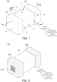
- FIG. 1 is a perspective view schematically illustrating a multilayer electronic component according to an embodiment.
- FIG. 2 is a perspective view schematically illustrating a structure in which a base electrode layer and an intermediate electrode layer are disposed on a body of a multilayer electronic component according to an embodiment.
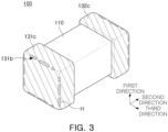
- FIG. 3 is a perspective view schematically illustrating a structure in which a base electrode layer, an intermediate electrode layer, and a conductive resin layer are disposed on a body of a multilayer electronic component according to an embodiment.
- FIG. 4 is a cross-sectional view schematically illustrating a cross section taken along line I-I' of FIG. 1 .
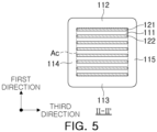
- FIG. 5 is a cross-sectional view schematically illustrating a cross section taken along line II-II' of FIG. 1 .
- FIG. 6 is an exploded perspective view schematically illustrating an exploded body of a multilayer electronic component according to an embodiment.
- FIG. 7 is an enlarged view of region K1 of FIG. 4 .
- FIG. 8 is an enlarged view of region K2 of FIG. 4 .
- a multilayer electronic component 100 may include a body 110 including a dielectric layer 111 and first and second internal electrodes 121 and 122 alternately disposed with the dielectric layer 111 interposed therebetween, and having first and second surfaces 1 and 2 opposing each other in the first direction, third and fourth surfaces 3 and 4 connected to the first and second surfaces 1 and 2 and opposing each other in the second direction, and fifth and sixth surfaces 5 and 6 connected to the first to fourth surfaces 1, 2, 3 and 4 and opposing each other in a third direction, the body 110 including a first corner C1 connecting the third surface 3 and the first, second, fifth, and sixth surfaces 1, 2, 5 and 6, respectively, and a second corner C2 connecting the fourth surface 4 and the first, second, fifth, and sixth surfaces 1, 2, 5 and 6, respectively; a first external electrode 131 including a first base electrode layer 131a disposed on the third surface 3, a first intermediate electrode layer 131b disposed on the first corner C1 and connected to the first base electrode layer 131a, a first external electrode 131 including a first base electrode
- At least a portion of the first intermediate electrode layer 131b may be in contact with the first plating layer 131d on the first corner C1, and at least a portion of the second intermediate electrode layer 132b may be in contact with the second plating layer 132d on the second corner C2.
- the multilayer electronic component 100 by including intermediate electrode layers 131b and 132b disposed on the corners C1 and C2 of the body 110 and conductive resin layers 131c and 132c disposed on the intermediate electrode layers, capacitance per unit volume may be secured, cracks due to mounting may be prevented, and penetration of a plating solution and/or external moisture through the corner of the body may be prevented.
- at least portions of the intermediate electrode layers 131b and 132b are in contact with the plating layers 131d and 132d on the corner of the body, thereby preventing an increase in ESR while preventing cracks due to mounting through the conductive resin layers 131c and 132c.
- the body 110 may have a hexahedral shape or a shape similar thereto. Due to shrinkage of the ceramic powder included in the body 110 during the sintering process or polishing of the corners, the body 110 may not have a hexahedral shape with perfect straight lines, but may substantially have a hexahedral shape.
- the body 110 may have first and second surfaces 1 and 2 opposing each other in the first direction, third and fourth surfaces 3 and 4 connected to the first and second surfaces 1 and 2 and opposing each other in the second direction, and fifth and sixth surfaces 5 and 6 connected to the first to fourth surfaces 1, 2, 3, and 4 and opposing each other in the third direction.
- the body 110 may include a first corner C1 connecting the third surface 3, the first surface 1, the second surface 2, the fifth surface 5, and the sixth surface 6, respectively, and include a second corner C2 connecting the fourth surface 4 to the first surface 1, the second surface 2, the fifth surface 5, and the sixth surface 6, respectively.
- the first corner C1 may include a 1-1-th corner C1-1 connecting the third surface 3 and the first surface 1, and a 1-2-th corner C1-2 connecting the third surface 3 and the second surface 2, and the second corner C2 may include a 2-3-th corner C2-1 connecting the fourth surface 4 and the first surface 1, and a 2-2-th corner C2-2 connecting the fourth surface 4 and the second surface 2.
- the first corner C1 may include a 1-5-th corner connecting the third and fifth surfaces 3 and 5, and a 1-6-th corner connecting the third surface 3 and the sixth surface 6, and the second corner C2 may include a 2-5-th corner connecting the fourth and fifth surfaces 4 and 5 and a 2-6-th corner connecting the fourth and sixth surfaces 4 and 6.
- the corner may have a round shape by rounding the corner connecting respective sides of the body 110 by performing a separate process.
- the first to sixth surfaces 1 to 6 of the body 110 may be substantially flat surfaces, and non-flat areas may be viewed as corners.
- dielectric layers 111 and internal electrodes 121 and 122 may be alternately stacked.
- the plurality of dielectric layers 111 forming the body 110 are in a sintered state, and a boundary between adjacent dielectric layers 111 may be unified to the extent that it is difficult to confirm without using a scanning electron microscope (SEM).
- SEM scanning electron microscope
- the dielectric layer 111 may be formed by preparing a ceramic slurry containing ceramic powder, an organic solvent and a binder, applying and drying the slurry on a carrier film to prepare a ceramic green sheet, and then by sintering the ceramic green sheet.
- the ceramic powder is not particularly limited as long as sufficient capacitance may be obtained, but, for example, barium titanate-based (BaTiO 3 )-based powder may be used.
- the average thickness td of the dielectric layer 111 is not particularly limited, but may be, for example, 10 ⁇ m or less.
- the average thickness td of the dielectric layer 111 may be arbitrarily set according to required characteristics or uses. For example, in the case of high-voltage electronic components, the average thickness td of the dielectric layer 111 may be less than 2.8 ⁇ m, and in the case of small IT electronic components, the average thickness td of the dielectric layer 111 may be 0.4 ⁇ m or less to obtain miniaturization and high capacitance, but the present disclosure is not limited thereto.
- the thickness of the dielectric layer 111 decreases, cracks are easily generated in the body 110 due to bending stress generated when voltage is applied. Accordingly, there is a problem in that the reliability of the multilayer electronic component is lowered.
- the external electrodes 131 and 132 include the base electrode layers 131a and 132a, the intermediate electrode layers 131b and 132b, and the conductive resin layers 131c and 132c, even when the average thickness td of the dielectric layer 111 is less than 2.8 um or 0.4 ⁇ m or less, the reliability of the multilayer electronic component may be improved.
- the average thickness td of the dielectric layer 111 refers to the size of the dielectric layer 111 disposed between the internal electrodes 121 and 122 in the first direction.
- the average thickness of the dielectric layer 111 may be measured by scanning a cross section of the body 110 in the first and second directions with a scanning electron microscope (SEM) at a magnification of 10, 000.
- SEM scanning electron microscope
- an average value may be measured by measuring the thickness at a plurality of points of one dielectric layer 111, for example, at 30 points equally spaced in the second direction. The 30 equally spaced points may be designated in a capacitance formation portion Ac to be described later.
- the average thickness of the dielectric layer 111 may be further generalized.
- the internal electrodes 121 and 122 may be alternately disposed with the dielectric layer 111.
- the first internal electrode 121 and the second internal electrode 122 which are a pair of electrodes having different polarities, may be disposed to face each other, with the dielectric layer 111 interposed therebetween.
- the plurality of first internal electrodes 121 and the plurality of second internal electrodes 122 may be electrically separated from each other by the dielectric layer 111 disposed therebetween.
- the plurality of first internal electrodes 121 may be spaced apart from the fourth surface 4 and connected to the third surface 3.
- the plurality of second internal electrodes 122 may be spaced apart from the third surface 3 and connected to the fourth surface 4.
- the conductive metal included in the internal electrodes 121 and 122 may be at least one of nickel (Ni), copper (Cu), palladium (Pd), silver (Ag), gold (Au), platinum (Pt), tin (Sn), tungsten (W), titanium (Ti) and alloys thereof, but the present disclosure is not limited thereto.
- the internal electrodes 121 and 122 may be formed by applying a conductive paste for internal electrodes containing a conductive metal to a predetermined thickness on a ceramic green sheet and sintering the same.
- a screen-printing method or a gravure printing method may be used as a printing method of the conductive paste for internal electrodes, but the present disclosure is not limited thereto.
- the average thickness te of the internal electrodes 121 and 122 is not particularly limited, but may be, for example, 3 ⁇ m or less.
- the average thickness te of the internal electrodes 121 and 122 may be arbitrarily set according to required characteristics or uses.
- the average thickness te of the internal electrodes 121 and 122 may be less than 1 ⁇ m, and in the case of small IT electronic components, the average thickness te of the internal electrodes 121 and 122 may be 0. 4 ⁇ m or less to obtain miniaturization and high capacitance, but the present disclosure is not limited thereto.
- the external electrodes 131 and 132 include the base electrode layers 131a and 132a, the intermediate electrode layers 131b and 132b, and the conductive resin layers 131c and 132c, even when the average thickness te of the internal electrodes 121 and 122 is less than 1 ⁇ m or 0.4 um or less, the reliability of the multilayer electronic component may be improved.
- the average thickness te of the internal electrodes 121 and 122 refers to the size of the internal electrodes 121 and 122 in the first direction.
- the average thickness of the internal electrodes 121 and 122 may be measured by scanning a cross section of the body 110 in the first and second directions with a scanning electron microscope (SEM) at a magnification of 10, 000.
- the average value may be measured by measuring the thicknesses at a plurality of points of one internal electrode 121 or 122, for example, at 30 points equally spaced in the second direction. The 30 equally spaced points may be designated in a capacitance formation portion Ac to be described later.
- the average thickness of the internal electrodes 121 and 122 may be further generalized.
- the body 110 may include a capacitance formation portion Ac which is disposed inside the body 110 and in which capacitance is formed by including first and second internal electrodes 121 and 122 alternately disposed with the dielectric layer 111 interposed therebetween, and a first cover portion 112 and a second cover portion 113 respectively disposed on both surfaces of the capacitance formation portion Ac, opposing each other in the first direction.
- the cover portions 112 and 113 may basically serve to prevent damage to the internal electrodes due to physical or chemical stress.
- the cover portions 112 and 113 may have the same configuration as the dielectric layer 111 except that they do not include internal electrodes.
- the body 110 may include margin portions 114 and 115 disposed on both surfaces of the capacitance formation portion Ac, opposing each other in the third direction.
- the margin portions 114 and 115 may refer to regions between both ends of the internal electrodes 121 and 122 and the boundary surface of the body 110 in the cross-section of the body 110 cut in the first and third directions.
- the margin portions 114 and 115 include a first margin portion 114 connected to the fifth surface 5 of the body 110 and a second margin portion 115 connected to the sixth surface 6 of the body 110.
- the margin portions 114 and 115 may include the same material as the dielectric layer 111 except that the internal electrodes 121 and 122 are not included.
- the margin portions 114 and 115 may basically serve to prevent damage to the internal electrodes 121 and 122 due to physical or chemical stress.
- the margin portions 114 and 115 may be formed by coating and sintering a conductive paste for internal electrodes on the ceramic green sheet, except where the margin portion is to be formed.
- the internal electrodes 121 and 122 are cut to be connected to the fifth and sixth surfaces 5 and 6 of the body after stacking, and then a single dielectric layer or two or more dielectric layers are stacked on both opposite surfaces of the capacitance forming portion Ac in the third direction, thereby forming the margin portions 114 and 115.
- the external electrodes 131 and 132 may be disposed on the third and fourth surfaces 3 and 4 of the body 110, and may extend onto portions of the first, second, fifth, and sixth surfaces 1, 2, 5 and 6.
- the external electrodes 131 and 132 may include a first external electrode 131 connected to the plurality of first internal electrodes 121 and a second external electrode 132 connected to the plurality of second internal electrodes 122.
- the area disposed on the third surface 3 may be defined as the first connection portion P1a
- the area disposed on the first and second surfaces 1 and 2 may be defined as the first band portion P1b
- the area between the first connection portion and the first band portion, disposed on the first corner C1 may be defined as the first corner portion P1c.
- the area disposed on the fourth surface 4 may be defined as a second connection portion P2a
- the area disposed on the first and second surfaces 1 and 2 may be defined as the second band portion P2b
- the area between the second connection portion and the second band portion, disposed on the second corner C2 may be defined as the second corner P2c.
- the first external electrode 131 may include a first base electrode layer 131a disposed on the third surface 3, a first intermediate electrode layer 131b disposed on the first corner C1 and connected to the first base electrode layer, a first conductive resin layer 131c disposed on the first intermediate electrode layer, and a first plating layer 131d disposed on the first conductive resin layer.
- the second external electrode 132 may include a second base electrode layer 132a disposed on the fourth surface 4, a second intermediate electrode layer 132b disposed on the second corner C2 and connected to the second base electrode layer, a second conductive resin layer 132c disposed on the second intermediate electrode layer, and a second plating layer 132d disposed on the second conductive resin layer.
- the first base electrode layer 131a may serve to connect the first internal electrode 121 and the first external electrode 131
- the second base electrode layer 132a may serve to connect the second internal electrode 122 and the second external electrode 132.
- the conductive metal included in the first and second base electrode layers 131a and 132a does not need to be particularly limited.
- the first and second base electrode layers 131a and 132a may include at least one of Ni, Cu, Cr, Sn, Pd, and alloys thereof, and in more detail, may include Ni.
- the internal electrodes 121 and 122 and the base electrode layers 131a and 132a contain Ni, the occurrence of radiation cracks due to the difference in diffusion rates of two different metals may be suppressed, and accordingly, bonding force between the internal electrodes 121 and 122 and the base electrode layers 131a and 132a may be secured.
- the first base electrode layer 131a may include a region not covered by the first intermediate electrode layer 131b, and the second base electrode layer 132a may include a region not covered by the second intermediate electrode layer 132b.
- the first base electrode layer 131a includes a region not covered by the first intermediate electrode layer 131b in the first connection portion P1a, and the second base electrode layer 132a may include a region not covered by the second intermediate electrode layer 132b in the second connection portion P2a. Accordingly, the capacitance per unit volume of the multilayer electronic component may be improved by reducing the thickness of the central region of the external electrodes 131 and 132 in the first direction.
- the first base electrode layer 131a and the first conductive resin layer 131c may be in contact with each other through a region of the first base electrode layer 131a that is not covered by the first intermediate electrode layer 131b.
- the second base electrode layer 132a and the second conductive resin layer 132c may contact each other through a region of the second base electrode layer 132a not covered by the second intermediate electrode layer 132b.
- the end of the first base electrode layer 131a is disposed on the first corner C1, and an end of the second base electrode layer 132a may be disposed on the second corner C2.
- an end of the first base electrode layer 131a may be disposed at the first corner portion P1c
- an end of the second base electrode layer 132a may be disposed at the second corner portion P2c.
- the plating solution and/or external moisture penetrating into the body 110 tends to penetrate into the corners C1 and C2 of the body 110 having a short distance to the internal electrodes.
- the ends of the first and second base electrode layers 131a and 132a are disposed on the corners C1 and C2 of the body 110, and penetration of the plating solution and/or external moisture into the corners C1 and C2 of the body 110 may be prevented.
- capacitance per unit volume of the multilayer electronic component may be secured by reducing the size of the multilayer electronic component in the first direction.
- the base electrode layers 131a and 132a may include glass to secure bonding strength with the body 110.
- the base electrode layers 131a and 132a may be formed by transferring sheets including conductive metal and glass onto the third and fourth surfaces 3 and 4, respectively, and then sintering the same.
- the base electrode layers 131a and 132a may be formed by compressing the body 110 to a sheet including conductive metal and glass, attaching the sheet to the body, and sintering the same.
- the present disclosure is not limited thereto, and the base electrode layers 131a and 132a may be Ni plating layers. In this case, the base electrode layers 131a and 132a may not include glass. When the base electrode layers 131a and 132a are Ni plating layers, as described above, radiation cracking may be prevented and bonding strength between internal electrodes may be secured. In this case, the base electrode layers 131a and 132a may be formed using an electrolytic plating method and/or an electroless plating method.
- the base electrode layers 131a and 132a when the base electrode layers 131a and 132a are Ni plating layers, the base electrode layers 131a and 132a may be disposed on both surfaces of the capacitance formation portion Ac opposing each other in the second direction, and ends of the base electrode layers 131a and 132a may be disposed on the cover portions 112 and 113 and/or the margin portions 114 and 115.
- the intermediate electrode layers 131b and 132b are basically disposed on the corners C1 and C2 of the body 110, and accordingly, the thickness of the central region of the external electrodes 131 and 132 in the first direction may not be excessively increased. Accordingly, a plating solution and/or external moisture may be prevented from penetrating into the corners C1 and C2 of the body 110 while securing the capacitance per unit volume of the multilayer electronic component.
- the method of forming the intermediate electrode layers 131b and 132b does not need to be particularly limited.
- the intermediate electrode layers 131b and 132b may be formed by applying a conductive paste containing a conductive metal and glass on the corners C1 and C2 of the body 110 and sintering the same.
- At least a portion of the first intermediate electrode layer 131b is in contact with the first plating layer 131d on the first corner C1, and on the second corner C2, at least a portion of the second intermediate electrode layer 132b may contact the second plating layer 132d.
- at least a portion of the first intermediate electrode layer 131b may be in contact with the first plating layer 131d at the first corner portion P1c.
- At least a portion of the second intermediate electrode layer 132b may contact the second plating layer 132d at the second corner portion P2c.
- the external electrodes 131 and 132 include the conductive resin layers 131c and 132c to prevent cracking due to mounting, there is a problem in which the ESR of the multilayer electronic component increases due to the conductive resin layers 131c and 132c having high resistance.
- At least portions of the intermediate electrode layers 131b and 132b on the corners C1 and C2 of the body 110 come into contact with the plating layers 131d and 132d to prevent cracks caused by mounting through the conductive resin layers 131c and 132c, and ESR may be prevented from increasing.
- ESR may be effectively reduced without affecting the reliability of multilayer electronic components.
- the contact point between the intermediate electrode layers 131b and 132b and the plating layers 131d and 132d may be on the corners C1 and C2 of the body 110 and need not be particularly limited.
- at least portions of the intermediate electrode layers 131b and 132b may contact the plating layers 131d and 132d on the corners C1 and C2 of the body 110.
- the method of bringing the intermediate electrode layers 131b and 132b into contact with the plating layers 131d and 132d does not need to be particularly limited.
- the first conductive resin layer 131c may include a first opening H disposed on the first corner C1, the first intermediate electrode layer 131b and the first plating layer 131d contact each other through the first opening
- the second conductive resin layer 132c may include a second opening disposed on the second corner C2
- the second intermediate electrode layer 132b and the second plating layer 132d may contact each other through the second opening.
- the conductive resin layers 131c and 132c may include a plurality of openings disposed at four peripheral sides of the corner portions P1c and P2c, and the intermediate electrode layers 131b and 132b may contact the plating layers 131d and 132d through the plurality of openings. That is, the plurality of first openings may be arranged along four peripheral sides of the first corner C1, and the plurality of second openings may be arranged along four peripheral sides of the second corner C2.
- the conductive resin layers 131c and 132c may include at least one opening disposed on the corners C1 and C2 of the body 110, and the opening may have any shape as long as it may bring the intermediate electrode layers 131b and 132b and the plating layers 131d and 132d into contact with each other.
- the method of forming the openings of the conductive resin layers 131c and 132c does not need to be particularly limited, and for example, after coating the conductive resin composition forming the conductive resin layers 131c and 132c on the intermediate electrode layers 131b and 132b, and before curing the conductive resin composition, the opening may be formed by removing at least a portion of the conductive resin composition applied on the corners C1 and C2 of the body 110.
- At least portions of the first and second intermediate electrode layers 131b and 132b may extend onto the first and second surfaces 1 and 2. In addition, at least portions of the first and second intermediate electrode layers 131b and 132b may extend onto the fifth and sixth surfaces 5 and 6. In detail, as illustrated in FIGS. 4 and 7 , at least portions of the first and second intermediate electrode layers 131b and 132b may directly contact the first and second surfaces 1 and 2. Accordingly, to secure bonding strength with the body 110, each of the first and second intermediate electrode layers 131b and 132b may include glass.
- the conductive metal included in the first and second intermediate electrode layers 131b and 132b does not need to be particularly limited, but for example, the first and second intermediate electrode layers 131b and 132b may include at least one of Cu, Ni, Cr, Sn, Pd, and alloys thereof.
- one end of the first intermediate electrode layer 131b and one end of the second intermediate electrode layer 132b may be respectively disposed on the capacitance formation portion Ac.
- the intermediate electrode layers 131b and 132b may be disposed to cover the outermost internal electrodes in the first direction. Accordingly, penetration of the plating solution and/or external moisture into the inside of the body through the outermost internal electrode may be suppressed.
- the intermediate electrode layers 131b and 132b may not cover remaining internal electrodes of the capacitance formation portion Ac except the outermost internal electrodes in the first direction.
- the conductive resin layers 131c and 132c are disposed on the intermediate electrode layers 131b and 132b, and at least portions of the first and second conductive resin layers 131c and 132c may extend onto the first and second surfaces 1 and 2. In addition, at least portions of the first and second conductive resin layers 131c and 132c may extend onto the fifth and sixth surfaces 5 and 6.
- the conductive resin layers 131c and 132c may include conductive metal and resin.
- the conductive metal included in the conductive resin layers 131c and 132c may serve to electrically connect the base electrode layers 131a and 132a and the intermediate electrode layers 131b and 132b.
- the conductive metal included in the conductive resin layers 131c and 132c does not need to be particularly limited, but may include, for example, at least one of Cu, Ni, Ag, Sn, Cr, and alloys thereof.
- the shape of the conductive metal included in the conductive resin layers 131c and 132c does not need to be particularly limited, but may include, for example, one or more of spherical particles and flake particles.
- the spherical particle may also include a shape that is not perfectly spherical, and may include a shape in which, for example, a length ratio between a major axis and a minor axis (long axis/short axis) is 1.45 or less.
- Flake-type particles mean particles having a flat and elongated shape, and are not particularly limited, and for example, the length ratio of the major axis to the minor axis (major axis/minor axis) thereof may be 1.95 or more.
- the lengths of the major and minor axes of the spherical particles and flake-shaped particles may be measured from an image obtained by scanning a cross-section of the multilayer electronic component cut in the first and second directions at the center thereof in the third direction with a scanning electron microscope (SEM).
- SEM scanning electron microscope
- the resin included in the conductive resin layers 131c and 132c may secure bonding and absorb shock.
- the conductive resin layers 131c and 132c may have relatively high flexibility. Accordingly, the multilayer electronic component may be protected from external physical shock or bending shock, and cracks may be prevented from occurring in multilayer electronic components by absorbing stress or tensile stress applied during mounting on a board.
- the resin included in the conductive resin layers 131c and 132c does not need to be particularly limited, but an insulating resin may be used.
- an insulating resin may be used.
- at least one of epoxy resin, acrylic resin, and ethyl cellulose may be included.
- the plating layers 131d and 132d may improve mounting characteristics.
- the type of the plating layers 131d and 132d is not particularly limited, and may be a plating layer including Ni, Sn, Pd, and/or alloys including the same, and may be formed of a plurality of layers.
- the plating layers 131d and 132d may be, for example, a Ni plating layer or a Sn plating layer, or may have a form in which a Ni plating layer and a Sn plating layer are sequentially formed.
- the plating layers 131d and 132d may include a plurality of Ni plating layers and/or a plurality of Sn plating layers.
- the first base electrode layer 131a, the first intermediate electrode layer 131b, and the first conductive resin layer 131c will be described as standards, and since the second external electrode 132 may have a symmetrical relationship with the first external electrode 131 in the second direction, descriptions of the first base electrode layer 131a, the first intermediate electrode layer 131b, and the first conductive resin layer 131c may be equally applied to the second base electrode layer 132a, the second intermediate electrode layer 132b, and the second conductive resin layer 132c.
- L2/L1 when the distance in the second direction from the third surface 3 to the end of the first intermediate electrode layer 131b disposed on the first or second surface 1 or 2 is L1 and when the distance from the third surface 3 to the end of the first conductive resin layer 131c disposed on the first or second surface 1 or 2 in the second direction is L2, L2/L1 may be greater than or equal to 2.5. When L2/L1 satisfies 2.5 or more, the effect of preventing penetration of plating solution and/or external moisture and reducing ESR may be more significant.
- the method of controlling the L1/L2 is not particularly limited. For example, by adjusting the amount of coating of the conductive paste forming the first intermediate electrode layer 131b on the first base electrode layer 131a or adjusting the amount of coating of the conductive resin composition forming the first conductive resin layer 131c on the first intermediate electrode layer 131c, L1/L2 may be controlled.
- L1/L2 may be measured by observing the cross-section of the multilayer electronic component cut in the first and second directions at the center thereof in the third direction using a scanning electron microscope (SEM) at a magnification of 2000 times or more.
- SEM scanning electron microscope
- tc when the thickness of the first intermediate electrode layer measured on the first corner C1 is tc, tc may be 2 ⁇ m or more. When the tc is greater than or equal to 2 um, penetration of the plating solution and/or external moisture through the first corner C1 of the body 110 may be more effectively prevented. In addition, when the tc is 2 ⁇ m or more, the first intermediate electrode layer 131b and the first plating layer 131d may more easily contact each other, and in this manner, the ESR may be effectively reduced.
- the tc may be the thickness of the first intermediate electrode layer 131b measured on the 1-1-th corner C1-1 or the thickness of the first intermediate electrode layer 131b measured on the 1-2-th corner C1-2.
- the tc may refer to a minimum thickness of the first intermediate electrode layer measured in a direction perpendicular to the surface of the 1-1-th corner C1-1 or 1-2-th corner C1-2.
- the tc may be measured by observing a section cut in the first and second directions at the center of the third direction of the multilayer electronic component using a scanning electron microscope (SEM) at a magnification of 3000 times or more.
- SEM scanning electron microscope
- t1'/t1 when the thickness of the first base electrode layer 131a measured at the center of the body 110 in the first direction is t1 and when the thickness of the first base electrode layer 131a measured at the internal electrode on the outermost portion of the body 110 in the first direction is disposed is t1', t1'/t1 may be greater than or equal to 0.8 and less than or equal to 1.0.
- the capacitance per unit volume of the multilayer electronic component may be improved, and reliability of the multilayer electronic component may be improved by preventing the external electrode from being formed too thin on the first corner C1 of the body 110.
- t2>t1 when the sum of the thicknesses of the first base electrode layer 131a and the first intermediate layer 131b measured on the internal electrode disposed on the outermost side of the body in the first direction is t2, t2>t1 may be satisfied.
- the external electrodes 131 and 132 may have a uniform thickness as a whole even when the first conductive resin layer 131c is formed on the first intermediate electrode layer 131b, and accordingly, the capacitance per unit volume of the multilayer electronic component may be improved and reliability of the multilayer electronic component may be improved by preventing the external electrode from being formed too thin on the first corner C1.
- t1 and t1' denote sizes of the first base electrode layer 131a in the second direction
- t2 denotes the sum of sizes of the first base electrode layer 131a and the first intermediate electrode layer 131b in the second direction.
- the method of controlling t2 to be greater than t1 and the method of controlling t1/t1' to be 0.8 or more and 1.0 or less do not need to be particularly limited.
- t2 may be controlled to be greater than t1
- t1/t1' may be controlled to be 0.8 or more and 1.0 or less.
- t1, t1' and t2 may be measured by observing the cross section cut in the first and second directions at the center of the third direction of the multilayer electronic component with a scanning electron microscope (SEM) at a magnification of 3000 times or more.
- SEM scanning electron microscope
- the multilayer electronic component according to an embodiment may have the same configuration as the above-described multilayer electronic component according to the embodiment. Therefore, description overlapping with the above-described embodiment will be omitted.
- the multilayer electronic component 100 includes a body 110 including a dielectric layer 111 and first and second internal electrodes 121 and 122 alternately disposed with the dielectric layer 111 interposed therebetween, and having first and second surfaces 1 and 2 opposing each other in a first direction, third and fourth surfaces 3 and 4 connected to the first and second surfaces 1 and 2 and opposing each other in a second direction, and fifth and sixth surfaces 5 and 6 connected to the first to fourth surfaces 1, 2, 3 and 4 and opposing each other in a third direction, the body 110 including a first corner C1 connecting the third surface 3 and the first, second, fifth, and sixth 1, 2, 5 and 6 surfaces, respectively, and a second corner C2 connecting the fourth surface 4 and the first, second, fifth, and sixth surfaces 1, 2, 5 and 6, respectively; a first external electrode 131 including a first base electrode layer 131a disposed on the third surface 3, a first intermediate electrode layer 131b disposed on the first corner C1 and connected to the first base electrode layer 131a, a first conductive resin layer 131
- the base electrode layers 131a and 132a include regions not covered by the intermediate electrode layers 131b and 132b, capacitance per unit volume of the multilayer electronic component is secured by reducing the thickness of the central region of the external electrodes 131 and 132 in the first direction.
- the intermediate electrode layers 131b and 132b disposed on the corners C1 and C2 of the body 110 prevent penetration of a plating solution and/or external moisture to improve reliability of the multilayer electronic component, and cracks due to mounting may be prevented by including the conductive resin layers 131c and 132c.
- a base electrode layer was formed by transferring a sheet including a conductive metal and glass to the body and then sintering the same, and by applying a conductive paste containing conductive metal and glass on the corner of the body on which the base electrode layer is formed and then sintering the same, an intermediate electrode layer was formed. Then, after applying the conductive resin composition to the body on which the intermediate electrode layer is formed, the intermediate electrode layer was exposed by partially removing the conductive resin composition applied to the central region of the corner of the body in the third direction. Thereafter, curing heat treatment was performed to form a conductive resin layer, and a plating layer was formed on the conductive resin layer to prepare a sample chip.
- L1 and L2 were measured through images obtained by scanning the cross section in the first and second directions at the center of the sample chip in the third direction with a scanning electron microscope (SEM).
- Table 1 below illustrates the number of moisture resistance defects and ESR measured and described according to L2/L1.
- ESR was measured at 1Mhz using a measuring instrument, and the maximum value of the ESR values measured in 400 samples for each test number is listed in Table 1 below.
- Table 1 Test No. L2/L1 Moisture Resistance Poor ESR (m ⁇ ) 1 1.5 3/400 7.22 2 2.0 3/400 6.83 3 2.5 0/400 4.34 4 2.7 0/400 4.72 5 3.0 0/400 4.73
- tc was measured through an image obtained by scanning a cross section of the sample chip in the first and second directions at the center in the third direction with a scanning electron microscope (SEM).
- tc was defined as the minimum thickness measured in the direction perpendicular to the surface of the corner of the body in the SEM image, and tc was measured on the 1-1-th corner or 1-2-th corner.
- Table 2 below lists the number of moisture resistance defects and ESR measured according to tc. Moisture resistance reliability evaluation and ESR were measured under the same conditions as the above after preparing 400 samples for each test number as described above. [Table 2] Test No. tc (pm) Moisture Resistance Poor ESR (mQ) 1 0.8 8/400 7.22 2 1.7 5/400 6.83 3 2.1 0/400 4.34 4 2.5 0/400 4.72 5 3.0 0/400 4.73
- cracks due to mounting may be prevented while securing capacitance per unit volume.
- Penetration of a plating solution and/or moisture into the body may be prevented while securing capacitance per unit volume.
- An increase in ESR may be prevented while preventing cracks due to mounting.
- first and second are used to distinguish one component from another, and do not limit the order and/or importance of the components.
- a first element may be named a second element, and similarly, a second element may be named a first element.
Landscapes
- Engineering & Computer Science (AREA)
- Power Engineering (AREA)
- Manufacturing & Machinery (AREA)
- Microelectronics & Electronic Packaging (AREA)
- Chemical & Material Sciences (AREA)
- Ceramic Engineering (AREA)
- Inorganic Chemistry (AREA)
- Fixed Capacitors And Capacitor Manufacturing Machines (AREA)
- Ceramic Capacitors (AREA)
Applications Claiming Priority (1)
| Application Number | Priority Date | Filing Date | Title |
|---|---|---|---|
| KR1020220111579A KR20240032511A (ko) | 2022-09-02 | 2022-09-02 | 적층형 전자 부품 |
Publications (2)
| Publication Number | Publication Date |
|---|---|
| EP4333003A2 true EP4333003A2 (de) | 2024-03-06 |
| EP4333003A3 EP4333003A3 (de) | 2024-05-29 |
Family
ID=87426642
Family Applications (1)
| Application Number | Title | Priority Date | Filing Date |
|---|---|---|---|
| EP23186353.1A Pending EP4333003A3 (de) | 2022-09-02 | 2023-07-19 | Mehrschichtiges elektronisches bauteil |
Country Status (5)
| Country | Link |
|---|---|
| US (1) | US12334269B2 (de) |
| EP (1) | EP4333003A3 (de) |
| JP (1) | JP2024035803A (de) |
| KR (1) | KR20240032511A (de) |
| CN (1) | CN117650011A (de) |
Families Citing this family (2)
| Publication number | Priority date | Publication date | Assignee | Title |
|---|---|---|---|---|
| KR20240032511A (ko) * | 2022-09-02 | 2024-03-12 | 삼성전기주식회사 | 적층형 전자 부품 |
| EP4557336A1 (de) * | 2023-11-16 | 2025-05-21 | Samsung Electro-Mechanics Co., Ltd. | Mehrschichtiges elektronisches bauteil |
Family Cites Families (28)
| Publication number | Priority date | Publication date | Assignee | Title |
|---|---|---|---|---|
| JPH08107039A (ja) | 1994-10-06 | 1996-04-23 | Murata Mfg Co Ltd | セラミック電子部品 |
| JP3307133B2 (ja) * | 1995-01-27 | 2002-07-24 | 株式会社村田製作所 | セラミック電子部品 |
| JP2010118499A (ja) | 2008-11-13 | 2010-05-27 | Murata Mfg Co Ltd | 積層セラミック電子部品 |
| JP4947076B2 (ja) * | 2009-03-25 | 2012-06-06 | Tdk株式会社 | 電子部品の製造方法 |
| KR101245347B1 (ko) * | 2011-12-29 | 2013-03-25 | 삼화콘덴서공업주식회사 | 적층 세라믹 커패시터 |
| JP2013165180A (ja) * | 2012-02-10 | 2013-08-22 | Tdk Corp | 電子部品及び電子部品の製造方法 |
| KR101422926B1 (ko) * | 2012-10-26 | 2014-07-23 | 삼성전기주식회사 | 적층 칩 전자부품 및 그 실장 기판 |
| JP6028739B2 (ja) * | 2013-03-07 | 2016-11-16 | 株式会社村田製作所 | 電子部品の製造方法 |
| KR102004776B1 (ko) * | 2013-12-05 | 2019-07-29 | 삼성전기주식회사 | 적층 세라믹 전자부품 및 그 실장 기판 |
| JP2018014447A (ja) * | 2016-07-22 | 2018-01-25 | 株式会社村田製作所 | 積層セラミック電子部品 |
| JP2018041761A (ja) * | 2016-09-05 | 2018-03-15 | 株式会社村田製作所 | チップ状電子部品 |
| JP2018088451A (ja) * | 2016-11-28 | 2018-06-07 | 株式会社村田製作所 | 積層セラミックコンデンサ |
| JP2018101724A (ja) * | 2016-12-21 | 2018-06-28 | 株式会社村田製作所 | 積層セラミックコンデンサ |
| KR101992450B1 (ko) * | 2017-08-23 | 2019-06-25 | 삼성전기주식회사 | 커패시터 부품 및 그 제조 방법 |
| JP7040063B2 (ja) * | 2018-01-31 | 2022-03-23 | Tdk株式会社 | 電子部品 |
| JP6841267B2 (ja) * | 2018-06-04 | 2021-03-10 | 株式会社村田製作所 | 積層セラミックコンデンサおよび積層セラミックコンデンサの実装構造 |
| JP2020107704A (ja) * | 2018-12-27 | 2020-07-09 | Tdk株式会社 | 電子部品 |
| JP7509514B2 (ja) * | 2018-12-27 | 2024-07-02 | Tdk株式会社 | 電子部品 |
| KR102620519B1 (ko) | 2019-04-17 | 2024-01-03 | 삼성전기주식회사 | 적층 세라믹 전자부품 |
| KR102762881B1 (ko) * | 2019-09-02 | 2025-02-07 | 삼성전기주식회사 | 적층 세라믹 전자부품 |
| KR102762882B1 (ko) * | 2019-09-02 | 2025-02-07 | 삼성전기주식회사 | 적층 세라믹 전자부품 |
| KR102760394B1 (ko) * | 2020-02-21 | 2025-02-03 | 삼성전기주식회사 | 적층형 전자 부품 |
| JP2022067931A (ja) * | 2020-10-21 | 2022-05-09 | Tdk株式会社 | 電子部品 |
| JP7659393B2 (ja) * | 2020-12-28 | 2025-04-09 | Tdk株式会社 | 電子部品 |
| JP2022183976A (ja) * | 2021-05-31 | 2022-12-13 | 株式会社村田製作所 | 電子部品 |
| KR20220163610A (ko) * | 2021-06-03 | 2022-12-12 | 삼성전기주식회사 | 적층형 커패시터 |
| KR102869401B1 (ko) * | 2021-12-13 | 2025-10-16 | 주식회사 아모텍 | 세라믹 커패시터 및 이의 제조방법 |
| KR20240032511A (ko) * | 2022-09-02 | 2024-03-12 | 삼성전기주식회사 | 적층형 전자 부품 |
-
2022
- 2022-09-02 KR KR1020220111579A patent/KR20240032511A/ko active Pending
-
2023
- 2023-07-19 EP EP23186353.1A patent/EP4333003A3/de active Pending
- 2023-07-19 US US18/223,739 patent/US12334269B2/en active Active
- 2023-07-31 JP JP2023124475A patent/JP2024035803A/ja active Pending
- 2023-08-25 CN CN202311083698.3A patent/CN117650011A/zh active Pending
Also Published As
| Publication number | Publication date |
|---|---|
| US12334269B2 (en) | 2025-06-17 |
| KR20240032511A (ko) | 2024-03-12 |
| JP2024035803A (ja) | 2024-03-14 |
| EP4333003A3 (de) | 2024-05-29 |
| US20240079182A1 (en) | 2024-03-07 |
| CN117650011A (zh) | 2024-03-05 |
Similar Documents
| Publication | Publication Date | Title |
|---|---|---|
| US11049661B2 (en) | Multilayer electronic component | |
| US11735374B2 (en) | Multi-layered ceramic electronic component | |
| US20140362492A1 (en) | Multilayer ceramic electronic component and method of manufacturing the same | |
| EP4333003A2 (de) | Mehrschichtiges elektronisches bauteil | |
| US20220165497A1 (en) | Multilayer electronic component | |
| CN114694951A (zh) | 电子组件 | |
| US12374498B2 (en) | Multilayer electronic component | |
| CN116417256A (zh) | 多层电子组件 | |
| EP4394825B1 (de) | GRENZFLÄCHENELEKTRODE ZWISCHEN INNEREN UND ÄUSSEREN ELEKTRODEN IN KERAMISCHEN MEHRSCHICHTKOMPONENTEN, BEI DENEN DREI ODER MEHR DER NICKELKÖRNER EINE KÖRNUNGSGRÖSSE VON 4 µM ODER GRÖSSER HABEN | |
| CN116417260A (zh) | 多层电子组件 | |
| EP4383293A2 (de) | Mehrschichtiges keramisches elektronisches bauteil | |
| KR20230103349A (ko) | 적층형 전자 부품 | |
| EP4386792A1 (de) | Mehrschichtiges elektronisches bauteil | |
| EP4216246A1 (de) | Mehrschichtiges elektronisches bauteil | |
| EP4435811A2 (de) | Mehrschichtiges elektronisches bauteil | |
| US12255020B2 (en) | Ceramic electronic component | |
| US20230215655A1 (en) | Multilayer electronic component | |
| KR20230112525A (ko) | 적층형 전자 부품 | |
| CN116469687A (zh) | 多层电子组件 |
Legal Events
| Date | Code | Title | Description |
|---|---|---|---|
| PUAI | Public reference made under article 153(3) epc to a published international application that has entered the european phase |
Free format text: ORIGINAL CODE: 0009012 |
|
| STAA | Information on the status of an ep patent application or granted ep patent |
Free format text: STATUS: THE APPLICATION HAS BEEN PUBLISHED |
|
| AK | Designated contracting states |
Kind code of ref document: A2 Designated state(s): AL AT BE BG CH CY CZ DE DK EE ES FI FR GB GR HR HU IE IS IT LI LT LU LV MC ME MK MT NL NO PL PT RO RS SE SI SK SM TR |
|
| PUAL | Search report despatched |
Free format text: ORIGINAL CODE: 0009013 |
|
| AK | Designated contracting states |
Kind code of ref document: A3 Designated state(s): AL AT BE BG CH CY CZ DE DK EE ES FI FR GB GR HR HU IE IS IT LI LT LU LV MC ME MK MT NL NO PL PT RO RS SE SI SK SM TR |
|
| RIC1 | Information provided on ipc code assigned before grant |
Ipc: H01G 4/30 20060101ALI20240423BHEP Ipc: H01G 4/12 20060101ALI20240423BHEP Ipc: H01G 4/012 20060101ALI20240423BHEP Ipc: H01G 4/232 20060101AFI20240423BHEP |
|
| STAA | Information on the status of an ep patent application or granted ep patent |
Free format text: STATUS: REQUEST FOR EXAMINATION WAS MADE |
|
| 17P | Request for examination filed |
Effective date: 20241121 |
|
| RBV | Designated contracting states (corrected) |
Designated state(s): AL AT BE BG CH CY CZ DE DK EE ES FI FR GB GR HR HU IE IS IT LI LT LU LV MC ME MK MT NL NO PL PT RO RS SE SI SK SM TR |