EP4328596A2 - Integrated circuit margin measurement and failure prediction device - Google Patents
Integrated circuit margin measurement and failure prediction device Download PDFInfo
- Publication number
- EP4328596A2 EP4328596A2 EP23220748.0A EP23220748A EP4328596A2 EP 4328596 A2 EP4328596 A2 EP 4328596A2 EP 23220748 A EP23220748 A EP 23220748A EP 4328596 A2 EP4328596 A2 EP 4328596A2
- Authority
- EP
- European Patent Office
- Prior art keywords
- output
- circuit
- computer
- comparison
- signal path
- Prior art date
- Legal status (The legal status is an assumption and is not a legal conclusion. Google has not performed a legal analysis and makes no representation as to the accuracy of the status listed.)
- Pending
Links
- 238000005259 measurement Methods 0.000 title claims description 22
- 238000003860 storage Methods 0.000 claims abstract description 49
- 230000003111 delayed effect Effects 0.000 claims abstract description 45
- 230000001934 delay Effects 0.000 claims description 20
- 230000008859 change Effects 0.000 claims description 10
- 238000012986 modification Methods 0.000 claims description 7
- 230000004048 modification Effects 0.000 claims description 7
- 230000009471 action Effects 0.000 claims description 3
- 230000000116 mitigating effect Effects 0.000 abstract description 35
- 239000004065 semiconductor Substances 0.000 abstract description 18
- 238000004458 analytical method Methods 0.000 description 69
- 238000000034 method Methods 0.000 description 63
- 230000015556 catabolic process Effects 0.000 description 36
- 238000006731 degradation reaction Methods 0.000 description 33
- 238000010586 diagram Methods 0.000 description 22
- 230000007547 defect Effects 0.000 description 20
- 230000032683 aging Effects 0.000 description 17
- 238000013461 design Methods 0.000 description 15
- 230000005540 biological transmission Effects 0.000 description 12
- 238000004519 manufacturing process Methods 0.000 description 12
- 238000010801 machine learning Methods 0.000 description 10
- 230000015654 memory Effects 0.000 description 10
- 238000012360 testing method Methods 0.000 description 10
- 239000013598 vector Substances 0.000 description 10
- 230000006870 function Effects 0.000 description 9
- 230000003712 anti-aging effect Effects 0.000 description 8
- 238000001514 detection method Methods 0.000 description 7
- 238000002474 experimental method Methods 0.000 description 7
- 229910052751 metal Inorganic materials 0.000 description 7
- 239000002184 metal Substances 0.000 description 7
- 238000004088 simulation Methods 0.000 description 5
- 230000008901 benefit Effects 0.000 description 4
- 230000008569 process Effects 0.000 description 4
- 230000002829 reductive effect Effects 0.000 description 4
- DYCJFJRCWPVDHY-LSCFUAHRSA-N NBMPR Chemical compound O[C@@H]1[C@H](O)[C@@H](CO)O[C@H]1N1C2=NC=NC(SCC=3C=CC(=CC=3)[N+]([O-])=O)=C2N=C1 DYCJFJRCWPVDHY-LSCFUAHRSA-N 0.000 description 3
- 230000003679 aging effect Effects 0.000 description 3
- 238000012937 correction Methods 0.000 description 3
- 230000000694 effects Effects 0.000 description 3
- 230000007246 mechanism Effects 0.000 description 3
- 238000012545 processing Methods 0.000 description 3
- 231100000817 safety factor Toxicity 0.000 description 3
- 238000005070 sampling Methods 0.000 description 3
- 238000012216 screening Methods 0.000 description 3
- 230000035882 stress Effects 0.000 description 3
- 239000002800 charge carrier Substances 0.000 description 2
- 239000003795 chemical substances by application Substances 0.000 description 2
- 230000006835 compression Effects 0.000 description 2
- 238000007906 compression Methods 0.000 description 2
- 238000004590 computer program Methods 0.000 description 2
- 230000000593 degrading effect Effects 0.000 description 2
- 238000012938 design process Methods 0.000 description 2
- 238000011161 development Methods 0.000 description 2
- 230000018109 developmental process Effects 0.000 description 2
- 230000006872 improvement Effects 0.000 description 2
- 230000000670 limiting effect Effects 0.000 description 2
- 238000013508 migration Methods 0.000 description 2
- 238000012544 monitoring process Methods 0.000 description 2
- 238000013450 outlier detection Methods 0.000 description 2
- 238000000611 regression analysis Methods 0.000 description 2
- 230000000630 rising effect Effects 0.000 description 2
- 239000000758 substrate Substances 0.000 description 2
- 230000007704 transition Effects 0.000 description 2
- 238000009827 uniform distribution Methods 0.000 description 2
- 238000011144 upstream manufacturing Methods 0.000 description 2
- RYGMFSIKBFXOCR-UHFFFAOYSA-N Copper Chemical compound [Cu] RYGMFSIKBFXOCR-UHFFFAOYSA-N 0.000 description 1
- XUIMIQQOPSSXEZ-UHFFFAOYSA-N Silicon Chemical compound [Si] XUIMIQQOPSSXEZ-UHFFFAOYSA-N 0.000 description 1
- 238000007792 addition Methods 0.000 description 1
- 229910052782 aluminium Inorganic materials 0.000 description 1
- XAGFODPZIPBFFR-UHFFFAOYSA-N aluminium Chemical compound [Al] XAGFODPZIPBFFR-UHFFFAOYSA-N 0.000 description 1
- 238000003340 combinatorial analysis Methods 0.000 description 1
- 238000004891 communication Methods 0.000 description 1
- 230000000295 complement effect Effects 0.000 description 1
- 229910052802 copper Inorganic materials 0.000 description 1
- 239000010949 copper Substances 0.000 description 1
- 238000012936 correction and preventive action Methods 0.000 description 1
- 230000007423 decrease Effects 0.000 description 1
- 230000003247 decreasing effect Effects 0.000 description 1
- 230000001419 dependent effect Effects 0.000 description 1
- 230000008021 deposition Effects 0.000 description 1
- 239000003989 dielectric material Substances 0.000 description 1
- 230000005684 electric field Effects 0.000 description 1
- 238000005516 engineering process Methods 0.000 description 1
- 230000007613 environmental effect Effects 0.000 description 1
- 238000013213 extrapolation Methods 0.000 description 1
- 230000005669 field effect Effects 0.000 description 1
- 238000002347 injection Methods 0.000 description 1
- 239000007924 injection Substances 0.000 description 1
- 238000012423 maintenance Methods 0.000 description 1
- 230000007257 malfunction Effects 0.000 description 1
- 229910044991 metal oxide Inorganic materials 0.000 description 1
- 150000004706 metal oxides Chemical class 0.000 description 1
- 230000005012 migration Effects 0.000 description 1
- 239000000203 mixture Substances 0.000 description 1
- 230000003287 optical effect Effects 0.000 description 1
- 230000037361 pathway Effects 0.000 description 1
- 238000000206 photolithography Methods 0.000 description 1
- 238000011084 recovery Methods 0.000 description 1
- 230000009467 reduction Effects 0.000 description 1
- 230000002441 reversible effect Effects 0.000 description 1
- 229910052710 silicon Inorganic materials 0.000 description 1
- 239000010703 silicon Substances 0.000 description 1
- 230000001360 synchronised effect Effects 0.000 description 1
- 230000009897 systematic effect Effects 0.000 description 1
- 230000036962 time dependent Effects 0.000 description 1
- 238000012546 transfer Methods 0.000 description 1
- 230000009466 transformation Effects 0.000 description 1
- 238000012795 verification Methods 0.000 description 1
Images


Classifications
-
- G—PHYSICS
- G01—MEASURING; TESTING
- G01R—MEASURING ELECTRIC VARIABLES; MEASURING MAGNETIC VARIABLES
- G01R31/00—Arrangements for testing electric properties; Arrangements for locating electric faults; Arrangements for electrical testing characterised by what is being tested not provided for elsewhere
- G01R31/28—Testing of electronic circuits, e.g. by signal tracer
- G01R31/30—Marginal testing, e.g. by varying supply voltage
- G01R31/3016—Delay or race condition test, e.g. race hazard test
-
- G—PHYSICS
- G01—MEASURING; TESTING
- G01R—MEASURING ELECTRIC VARIABLES; MEASURING MAGNETIC VARIABLES
- G01R31/00—Arrangements for testing electric properties; Arrangements for locating electric faults; Arrangements for electrical testing characterised by what is being tested not provided for elsewhere
- G01R31/28—Testing of electronic circuits, e.g. by signal tracer
- G01R31/2851—Testing of integrated circuits [IC]
- G01R31/2855—Environmental, reliability or burn-in testing
- G01R31/2872—Environmental, reliability or burn-in testing related to electrical or environmental aspects, e.g. temperature, humidity, vibration, nuclear radiation
- G01R31/2881—Environmental, reliability or burn-in testing related to electrical or environmental aspects, e.g. temperature, humidity, vibration, nuclear radiation related to environmental aspects other than temperature, e.g. humidity or vibrations
-
- G—PHYSICS
- G01—MEASURING; TESTING
- G01R—MEASURING ELECTRIC VARIABLES; MEASURING MAGNETIC VARIABLES
- G01R31/00—Arrangements for testing electric properties; Arrangements for locating electric faults; Arrangements for electrical testing characterised by what is being tested not provided for elsewhere
- G01R31/28—Testing of electronic circuits, e.g. by signal tracer
- G01R31/317—Testing of digital circuits
- G01R31/3181—Functional testing
- G01R31/319—Tester hardware, i.e. output processing circuits
- G01R31/3193—Tester hardware, i.e. output processing circuits with comparison between actual response and known fault free response
-
- G—PHYSICS
- G01—MEASURING; TESTING
- G01R—MEASURING ELECTRIC VARIABLES; MEASURING MAGNETIC VARIABLES
- G01R31/00—Arrangements for testing electric properties; Arrangements for locating electric faults; Arrangements for electrical testing characterised by what is being tested not provided for elsewhere
- G01R31/28—Testing of electronic circuits, e.g. by signal tracer
- G01R31/2851—Testing of integrated circuits [IC]
-
- G—PHYSICS
- G01—MEASURING; TESTING
- G01R—MEASURING ELECTRIC VARIABLES; MEASURING MAGNETIC VARIABLES
- G01R31/00—Arrangements for testing electric properties; Arrangements for locating electric faults; Arrangements for electrical testing characterised by what is being tested not provided for elsewhere
- G01R31/28—Testing of electronic circuits, e.g. by signal tracer
- G01R31/317—Testing of digital circuits
- G01R31/3181—Functional testing
- G01R31/319—Tester hardware, i.e. output processing circuits
- G01R31/3193—Tester hardware, i.e. output processing circuits with comparison between actual response and known fault free response
- G01R31/31937—Timing aspects, e.g. measuring propagation delay
-
- G—PHYSICS
- G01—MEASURING; TESTING
- G01R—MEASURING ELECTRIC VARIABLES; MEASURING MAGNETIC VARIABLES
- G01R31/00—Arrangements for testing electric properties; Arrangements for locating electric faults; Arrangements for electrical testing characterised by what is being tested not provided for elsewhere
- G01R31/50—Testing of electric apparatus, lines, cables or components for short-circuits, continuity, leakage current or incorrect line connections
- G01R31/52—Testing for short-circuits, leakage current or ground faults
Definitions
- the invention relates to the field of integrated circuits.
- Integrated circuits may include analog and digital electronic circuits on a flat semiconductor substrate, such as a silicon wafer. Microscopic transistors are printed onto the substrate using photolithography techniques to produce complex circuits of billions of transistors in a very small area, making modern electronic circuit design using ICs both low cost and high performance. ICs are produced in assembly lines of factories, termed foundries, that have commoditized the production of ICs, such as complementary metal-oxide-semiconductor (CMOS) ICs. Digital ICs contain billions of transistors arranged in functional and/or logical units on the wafer, with data-paths interconnecting the functional units that transfer data values between the functional units.
- CMOS complementary metal-oxide-semiconductor
- data-path means a parallel series of electronic connections, or paths, for transferring data signals between functional/logical units of an IC, and each data-path may include a specific number of bit paths, such as 64, 128, 256, ort the like.
- the timing of the functional units is arranged so that each functional unit may usually complete the required processing of that unit within a single clock cycle.
- a safety factor may be used to account for manufacturing differences of individual ICs and possible changes, such as degradations, over the planned lifetime of the IC.
- the degrading of an IC's transistors over time is termed aging.
- the degradation of transistors over time leads slowly to decreased switching speeds, and may even result in outright circuit failures, when they exceed the design safety factors.
- the design process incorporates these delays into the design such that the ICs will not fail during their normal lifetime, but environmental and usage conditions (such as heat, voltage, current, humidity, and/or the like) may accelerate the aging process.
- IC transistors such as bipolar transistors, metal-oxide semiconductor field-effect transistors (MOSFETs), and/or the like, may be used in digital ICs and may function as electrical switches.
- MOSFET metal-oxide semiconductor field-effect transistors
- a MOSFET may have four terminals, such as the body, the gate, the source, and the drain, yet typically the source and body are electrically connected.
- the voltage applied to the gate may determine the amount of current that flows between the source and drain.
- a thin layer of dielectric material electrically insulates the gate, and the electric field applied across the gate may alter the conductivity of the underlying semiconductor channel between the source and drain.
- HCI hot-carrier injection
- BTI bias temperature instability
- Another aging mechanism comes into play when a voltage applied to the gate may create electrically active defects, known as traps, within the dielectric. When traps become too numerous, these charge traps may join and form an outright short circuit between the gate and the current channel. This kind of failure is termed oxide breakdown, or time-dependent dielectric breakdown. Unlike the other aging mechanisms, which cause a gradual decline in performance, the breakdown of the dielectric may lead to a catastrophic failure of the transistor, causing the IC to malfunction.
- Electromigration may damage the copper or aluminum connections that tie transistors together or link them to the outside world. Electromigration may occur when a surge of current knocks metal atoms loose from the electrical connections, and may cause them to flow with the electrons. This depletes the metal of some atoms upstream, while causing a buildup of metal downstream. The upstream thinning of the metal increases the electrical resistance of the connection, sometimes becoming an open circuit. The downstream deposition may cause the metal to bulge out of its designated track.
- any defect such as un-modeled phenomenon, random manufacturing defects, and/or the like, may cause a timing degradation of a signal path over time.
- Some defects may not appear during testing, verification, initial operation, and/or the like, for example, the die/IC/product may pass all the screening procedures at the testing stage.
- a via that includes a manufacturing defects, such as less that complete metal coverage, will increase its resistance over time and at some point, causes a timing failure of a logic path.
- random manufacturing defects may appear anywhere on the IC, and incorporate a large variety of types and levels of defects, so designs may not be able to incorporate safety factors to mitigate these defects.
- aspects of embodiments of the disclosed techniques may be able to predict the failure of each individual IC based on fingerprint sampling at appropriate IC pathways, and mitigate the failure by preemptive replacement, corrective and preventative actions, notifications to users, compensations within the IC to increase time lifetime, and/or the like.
- a semiconductor integrated circuit in accordance with the claims.
- This may comprise a signal path combiner, comprising a plurality of input paths and an output path.
- the IC comprises a delay circuit having an input electrically connected to the output path, the delay circuit delaying an input signal by a variable delay time to output a delayed signal path.
- the IC may comprise a first storage circuit electrically connected to the output path and a second storage circuit electrically connected to the delayed signal path.
- the IC comprises a comparison circuit that compares outputs of the first and second storage circuits, wherein the comparison circuit comprises a second output path electrically connected to one or more mitigation circuit.
- the mitigation circuit is one or more circuit from the group consisting of: a notification circuit; a timing delay measurement (or estimation) circuit; a data transmission circuit; an IC anti-aging compensation circuit; and a failure analysis circuit.
- the signal path combiner is one or more from the group consisting of a logical XOR combiner, a Hamming parity combiner, and multiplexer.
- variable delay time is set in an integer multiple of increments equal to a clock period of the IC divided by a signature vector size, and wherein the signature vector size is between 1 and 100,000.
- the mitigation circuit is a data transmission circuit electrically connected to a computerized server, wherein the computerized server is configured to receive multiple instances of the comparison data signal, perform a failure prediction analysis of the comparison data signals, and send a notification a mitigation module when the failure prediction analysis predicts failure of the IC within a predefined time.
- At least some of the comparison data signals are generated at multiple values of the variable delay time.
- At least some of the comparison data signals are generated from multiple instances of one or more value from multiple values of the variable delay time.
- the failure prediction analysis comprises one or more of a machine learning analysis, a trend analysis, a multiple object tracking analysis, and a multivariant analysis.
- the failure prediction analysis comprises receiving comparison data signals from multiple different ICs.
- the failure prediction analysis comprises receiving failure prediction analysis results from multiple different ICs.
- a semiconductor integrated circuit comprising: a signal path combiner, comprising a plurality of input paths and an output, the output being based on a combination of respective signals received on each of the input paths; a delay circuit having an input electrically connected to the signal path combiner output, the delay circuit delaying an input signal by a variable delay time to output a delayed signal; and a comparison circuit arranged to provide a comparison output based on a comparison of the signal path combiner output and the delayed signal, wherein the comparison output is provided in a comparison data signal to at least one mitigation circuit.
- the mitigation circuit is at least one circuit from the group consisting of: a notification circuit; a timing delay measurement circuit; a data transmission circuit; an IC anti-aging compensation circuit; and a failure analysis circuit.
- the signal path combiner is at least one from the group consisting of a logical XOR combiner, a Hamming parity combiner, and multiplexer.
- the IC further comprises: a first internal storage circuit, electrically connected to the signal path combiner output and arranged to provide the stored signal path combiner output as a first input to the comparison circuit; and a second internal storage circuit, electrically connected to the delayed signal and arranged to provide the delayed signal as a second input to the comparison circuit.
- the signal path combiner is a first signal path combiner arranged to receive a plurality of signals from a first data source and the comparison circuit is a first comparison circuit.
- the IC may further comprise: a second signal path combiner, comprising a plurality of input paths and an output, the second signal path combiner output being based on a combination of respective signals received on each of the input paths, the signals being received from a second data source; a multiplexer, configured to receive the first signal path combiner output, the second signal path combiner output and a selection signal and to selectively output the first signal path combiner output or the second signal path combiner output based on the selection signal, the output of the multiplexer being provided as the input to the delay circuit; a second comparison circuit arranged to provide a second comparison output based on a comparison of the second signal path combiner output and the delayed signal; and an OR gate arranged to receive as inputs the first comparison output and the second comparison output and to provide an output as the comparison data signal to the at least one mitigation circuit
- the IC optionally, further comprises: a first comparison storage circuit, arranged to receive the first comparison output and controlled by a first clock signal; a second comparison storage circuit, arranged to receive the second comparison output and controlled by a second clock signal; and wherein the first comparison storage circuit is arranged to provide the first comparison output as a first input to the OR gate and the second comparison storage circuit is arranged to provide the second comparison output as a second input to the OR gate.
- variable delay time is set in an integer multiple of increments equal to a clock period of the IC divided by a signature vector size, and wherein the signature vector size is between 1 and 100,000.
- the mitigation circuit is a data transmission circuit electrically connected to a computerized server, wherein the computerized server is configured to receive multiple instances of the comparison data signal, perform a failure prediction analysis of the comparison data signals, and send a notification to a mitigation module when the failure prediction analysis predicts failure of the IC within a predefined time.
- the comparison data signals are generated at multiple values of the variable delay time.
- at least some of the comparison data signals are generated from multiple instances of at least one value from multiple values of the variable delay time.
- the failure prediction analysis comprises at least one of a machine learning analysis, a trend analysis, a multiple object tracking analysis, and a multivariant analysis.
- the failure prediction analysis comprises receiving comparison data signals from multiple different ICs.
- the failure prediction analysis comprises receiving failure prediction analysis results from multiple different ICs.
- each of the plurality of input paths of the signal path combiner is configured to receive one of: a signal from a respective data source in the IC; a signal from a memory circuit; and a signal from one of a plurality of logic circuits grouped by a clock enable.
- a method for using a semiconductor integrated circuit comprising: combining respective signals received on each of a plurality of input paths at a signal path combiner to provide an output; delaying the signal path combiner output by a variable delay time at a delay circuit to output a delayed signal; and comparing the signal path combiner output and the delayed signal to provide a comparison output and providing the comparison output in a comparison data signal to at least one mitigation circuit.
- the mitigation circuit is at least one circuit from the group consisting of: a notification circuit; a timing delay measurement circuit; a data transmission circuit; an IC anti-aging compensation circuit; and a failure analysis circuit.
- the signal path combiner is at least one from the group consisting of a logical XOR combiner, a Hamming parity combiner, and multiplexer.
- the method further comprises: storing the signal path combiner output at a first internal storage circuit and providing the stored signal path combiner output from the first internal storage circuit as a first input to the comparison circuit; and storing the delayed signal at a second internal storage circuit and providing the delayed signal from the second internal storage circuit as a second input to the comparison circuit.
- the signal path combiner is a first signal path combiner that receives a plurality of signals from a first data source and wherein the comparison circuit is a first comparison circuit. Then, the method may further comprise: combining respective signals received on each of a plurality of input paths at a second signal path combiner to provide an output, the signals being received from a second data source; receiving the first signal path combiner output, the second signal path combiner output and a selection signal at a multiplexer and selectively outputting the first signal path combiner output or the second signal path combiner output based on the selection signal, the output of the multiplexer being provided as the input to the delay circuit such that the step of delaying comprises delaying the first signal path combiner output or the second signal path combiner output by the variable delay time at the delay circuit to output the delayed signal; comparing the second signal path combiner output and the delayed signal to provide a second comparison output; and receiving at an OR gate, the first comparison output and the second comparison output as inputs and outputting the comparison data signal as an output from
- the method further comprises: receiving the first comparison output at a first comparison storage circuit controlled by a first clock signal; receiving the second comparison output at a second comparison storage circuit controlled by a second clock signal; providing the first comparison output from the first comparison storage circuit as a first input to the OR gate; and providing the second comparison output from the second comparison storage circuit as a second input to the OR gate.
- variable delay time is set in an integer multiple of increments equal to a clock period of the IC divided by a factor from 1 to 100,000.
- the mitigation circuit is a data transmission circuit electrically connected to a computerized server, the method further comprising: receiving multiple instances of the comparison data signal at the computerized server; performing a failure prediction analysis of the comparison data signals at the computerized server; sending a notification from the computerized server to a mitigation module when the failure prediction analysis predicts failure of the IC within a predefined time.
- at least some of the comparison data signals are generated at multiple values of the variable delay time.
- at least some of the comparison data signals are generated from multiple instances of at least one value from multiple values of the variable delay time.
- the failure prediction analysis comprises at least one of a machine learning analysis, a trend analysis, a multiple object tracking analysis, and a multivariant analysis.
- the failure prediction analysis comprises receiving comparison data signals from multiple different ICs.
- the failure prediction analysis comprises receiving failure prediction analysis results from multiple different ICs.
- each of the plurality of input paths of the signal path combiner is configured to receive one of: a signal from a respective data source in the IC; a signal from a memory circuit; and a signal from one of a plurality of logic circuits grouped by a clock enable.
- the method is performed at an initial operation of the IC. Then, the method may further comprise: measuring a timing delay for the IC, based on the comparison data signal provided to the mitigation circuit.
- the method further comprises: repeating the steps of combining, delaying and comparing for each of a plurality of delay times, in order to provide a plurality of comparison outputs; and determining an identifying characteristic for the IC based on the plurality of comparison outputs.
- the method further comprises: tracking changes in the identifying characteristic for the IC over time.
- a dedicated circuit which may be detector
- FPC failure prediction circuit
- MFPC margin measurement and failure prediction circuit
- a dedicated circuit is placed at selected points along one or more data-paths in a digital integrated circuit (such as one or more FPC or MFPC per data-path), where each dedicated circuit combines multiple individual data paths into a fewer number of test paths.
- a fingerprint or signature of the delays of each path of the data-path may be acquired during each clock cycle of the functional unit.
- fingerprint and/or “signature” mean the profile of signal strengths, such as a vector, series, and/or the like, resulting from a measurement of timing delay margins of a combination of signals of a data-path.
- margin refers to the timing delay of an individual data signal of the data-path. For each clock cycle of the functional unit the output data-path may have a different data value.
- a different combination of the logical paths within the functional unit may be tested, producing a different fingerprint.
- a dataset of fingerprints may be analyzed. The analysis of the fingerprint datasets may determine the performance and/or predict future failure of the individual IC.
- a semiconductor integrated circuit comprising: a signal path combiner, comprising a plurality of input paths (for example to receive signals on a data source or data-path, from a memory circuit and/or from logic circuits grouped by a clock enable) and an output, the output being based on a combination of respective signals received on each of the input paths; a delay circuit having an input electrically connected to the signal path combiner output, the delay circuit delaying an input signal by a variable delay time to output a delayed signal; and a comparison circuit arranged to provide a comparison output based on a comparison of the signal path combiner output and the delayed signal, wherein the comparison output is provided in a comparison data signal to at least one mitigation circuit.
- the combination of the signal path combiner, delay circuit and comparison circuit may provide an FPC or MFPC.
- a method for using such an IC may also be considered (in which using may comprise one of more of operating, analyzing and configuring, for instance).
- this may include a method for using a semiconductor integrated circuit (IC).
- the method may comprise: combining respective signals received on each of a plurality of input paths at a signal path combiner to provide an output; delaying the signal path combiner output by a variable delay time at a delay circuit to output a delayed signal; and comparing the signal path combiner output and the delayed signal to provide a comparison output and providing the comparison output in a comparison data signal to at least one mitigation circuit.
- the steps of combining, delaying and comparing may be repeated for each of a plurality of delay times.
- a plurality of comparison outputs may be provided.
- An identifying characteristic i.e. a signature or fingerprint
- the fingerprints may then be tracked at different times, for example by tracking changes in the fingerprint over time (using intervals at least as long as the length of time taken to determine a single fingerprint and preferably longer).
- a data-path is one example of a design style that can be handled by the FPC or MFPC, other examples may be memory circuits (the FPC/MFPC is located at the output of the memory) and other logic circuits that are grouped together with respect to a certain clock enable.
- aspects of embodiments described herein may be applied to any reliability problem of IC performance, such as aging, latent defects that manifest in the design and cause degradation, manufacturing differences within/between ICs, manufacturing differences between fabs, and/or the like.
- the techniques described may find changes in timing delays from any source or cause, predict a future failure before the IC failure causes a device/system failure, and enable corrective and preventive action before the specific IC failure. While reliability issues, such as aging, electro-migration, and/or the like, are used here as examples, the techniques may also be applied to latent defects, such as random defects, systematic defects, unknown defects, and/or the like.
- the delay me be changed in small time steps, producing one or more sweeps of time delays, and associated fingerprints at each different time delay.
- the sweep may be analyzed to determine the operation of the individual IC, predict a future failure of the IC, and/or the like.
- one or more datasets may be analyzed combinatorically to determine the operational delays of each path of the data-path (or equivalent signal path), each logical processing path of the functional unit, and/or the like.
- one or more datasets may be analyzed statistically to predict a future failure the IC.
- an IC degradation trend may be analyzed in one or more delay margins measured using the failure prediction circuit, such as be analyzing a minimum delay margin change over time.
- one or more datasets may be analyzed using machine learning to monitor the failure of the IC, predict a future failure of the IC, and/or the like.
- one or more datasets may be analyzed to design a future IC.
- one or more sweeps may be analyzed combinatorically to determine the operational delays of each path of the data-path, each logical processing path of the functional unit, and/or the like.
- one or more sweeps may be analyzed statistically to predict a future failure the IC. For example, a regression analysis of one or more sweeps determines the changes in timing delays, and an extrapolation to a timing delay failure value determines the time to failure.
- one or more sweeps may be analyzed using machine learning to monitor the failure of the IC, predict a future failure of the IC, and/or the like.
- one or more delay time sweeps may be analyzed to design a future IC, where the future IC is designed to avoid the failures of the previous ICs.
- one or more sweeps are analyzed using machine learning at the beginning-of-life of the chip, e.g. the timing delay margins signature or fingerprint of the IC at the beginning-of-life.
- the signature or fingerprint may be used for chip outlier detection/screening, i.e. a specific IC is given a unique identity and the signature as compared to other ICs that allows detecting anomaly's in a large manufacturing scale.
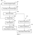
- FIG. 1 and FIG. 2 show schematically a computerized system 100 and flowcharts (200 and 210) of methods, respectively, for IC failure prediction and margin measurement of logic-paths at the IC testing (tester or system level).
- System 100 comprises an IC 150, a computer 101A, and a data interface connection 140 connecting the two.
- IC 150 comprises multiple function units (as at 151, 152, 153, and the like), and data-paths (as at 141, 142A, 142B, 143A, 143B, and the like, which may include synthesized logic) between them.
- IC 150 comprises margin measurement and failure prediction circuits (MFPCs; as at 131, 132, 133, and the like) for capturing signals from data-paths (as at 142A, 143A, and the like), and determining delay timings of at least some signals form the respective data-path.
- MFPCs 131, 132, or 133 combine 201 signals from the data-path, and test 202 one or more delays of the combined signals.
- IC 150 comprises a data interface for connecting to data interface connection 140, and sending 202 the delay timings to computer 101A. Delay timing data collected for multiple signals of the data-paths and/or for multiple delay values, such as be changing 204 the delay, may be considered the fingerprint of the delay timings.
- Computer 101A comprises one or more hardware processors 101B, a user interface 120 and a non-transitory, computer readable storage medium 102.
- Storage medium comprises program code, such as an MFPC Data Receiver 102A, an IC Aging Analyzer 102B, an IC Failure Predictor 102C, and/or the like, the program code comprising instructions that when executed on hardware processor(s) 101B, cause hardware processor(s) 101B to receive 211 the signal delay data (i.e. fingerprints) using a data interface 110, such as using MFPC Data Receiver 102A.
- IC Aging Analyzer 102B analyzes 212 the fingerprints, and IC Failure Predictor 102C notifies 213 an operator of a status, a failure prediction, a preventative action, and or the like, such as using user interface 120.
- the delay timings are analyzed by a circuit (not shown) of IC 150 to determine when clock and/or logic modifications 206 on IC 150 improve the lifetime of IC 150 before failure.
- the delay timings are analyzed by a circuit (not shown) of IC 150 and a notification 206 is issued of the status or failure prediction.
- the delay timing fingerprint may be generated at the IC testing (tester or system) to extract the time-zero margin map of the data-paths in a certain unit.
- the fingerprint may be analyzed at a time of initial operation and monitored over the life of the IC to determine when a predicted failure may occur. For example, a defect degradation gradient analysis may determine the future time of a failure of the IC. For example, analyzing the minimum margin of a fingerprint, plotting the minimum margin over time, and extrapolating the plot to a margin delay of zero determines the predicted time of failure.
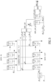
- FIG. 3 shows a XOR-based circuit diagram for IC failure prediction.
- An XOR component (XOR1) combines the signals from a data-path, such as 64, 128, 256, 512, or the like number of signals in to a single signal XOR1_out.
- XOR1_out is feed into a first flip-flop FF2, and a delay line D2.
- the delayed XOR1_out is fed into a second flip-flop FF1.
- FF1 and FF2 are activated by a clock clk_3, and their outputs XOR combined with XOR2.
- XOR2_out is a logical 1 for each delay where one of XOR1_out and XOR1_out_d2 is logical 1 at time of clk_d1.
- multiple instances of clk_d1 may and/or multiple values of D1 may determine timing delay data of the delay along data-paths of combinatorial (Combinatoric) logic FU1, and thus the fingerprint of timing delays.
- the MFPC may detect which of the paths of FU1 is degrading and/or aging fastest, and may cause failure of IC 150.
- the output signal of XOR1 may be considered a compression of the input signals that preserves the minimum timing margin delays of the input signals of the data-path.
- the output of XOR2 may be logic-1 when the minimum margin of an input signal is smaller than the delay associated with D2.
- XOR1 may be a parity checker, i.e. the output is logical 1 when the parity of the input signals is logical 1.
- Each rising-edge of the compressed signal (XOR1 output) may be associated with a rising edge of one of the input signals.
- the last rising or falling transitions of XOR1-output represents the minimal margin.
- This concept may be proven by a mathematical proof, described hereinbelow, as well as by event-based simulations. For example, special cases may be proved by simulation, where the margin of several signals is smaller than D2, multiple signals switched simultaneously, and/or the like.
- the IC may further comprise: a first internal storage circuit, electrically connected to the signal path combiner output and arranged to provide the stored signal path combiner output as a first input to the comparison circuit; and a second internal storage circuit, electrically connected to the delayed signal and arranged to provide the delayed signal as a second input to the comparison circuit.
- a first internal storage circuit electrically connected to the signal path combiner output and arranged to provide the stored signal path combiner output as a first input to the comparison circuit
- a second internal storage circuit electrically connected to the delayed signal and arranged to provide the delayed signal as a second input to the comparison circuit.
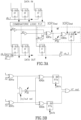
- FIG. 3A shows a different version of a XOR-based circuit diagram for IC failure prediction, in comparison with that shown in FIG. 3 .
- the data-path shown in FIG. 3A has essentially the same structure as that shown in FIG. 3 .
- a XOR component XOR1a combines the signals from the data-path, such as 64, 128, 256, 512, or the like number of signals, into a single output signal, XOR1a out .
- XOR1a out is fed as a first a first input to a second XOR circuit XOR2a and in parallel, to a delay-line D2, the output of which provides a second input to the second XOR circuit XOR2a.
- the delayed output signal from the second XOR circuit XOR2a, XOR2a out is fed into a flip-flop FF1b.
- Flip-flop FFlb is activated by a clock (clkla).
- the second output signal XOR2a out is a logical 1 for each delay where the two inputs of the second XOR circuit XOR2a are at different logic state at time of clkla.
- FIG.3B shows a further different version of a XOR-based circuit diagram for IC failure prediction, in comparison with that shown in FIG. 3 .
- two XOR-based failure prediction circuits are provided that use one delay-line circuit.
- two data-paths are provided, each of which may be in accordance with that shown in FIG. 3 or FIG. 3A .
- the first failure prediction circuit comprises: a first XOR component XOR1a that is driven by a set of parallel-input signals from a first data-path (as discussed with reference to FIG. 3 or FIG.
- the second failure prediction circuit comprises: a third XOR component XORlb that is driven by a set of parallel-input signals from a second data-path (as discussed with reference to FIG. 3 or FIG. 3A above); a fourth XOR component XOR2b; and a second flip-flop FFlb that is clocked by a second clock signal clklb.
- a common delay-line D2 serves the two failure prediction circuits with a multiplexer mux selecting, in a time-sharing mode, whether the output of the first XOR component XOR1a or the output of the third XOR component XORlb is provided as an input to the common delay-line D2. This is controlled using a selection signal In/out sel.
- the configuration of each of the two failure prediction circuits is otherwise as shown in FIG. 3A .
- the output of the first flip-flop FFlb clocked by first clock signal clkla and the output of the second flip-flop FFlb clocked by second clock signal clklb are provided as inputs to an OR gate to generate an output signal MT-out.
- output signal MT-out is a logical 1 for each delay where the two inputs of the second XOR component XOR2a are at different logic state at time of the first clock signal clkla.
- output signal MT-out is a logical 1 for each delay where the two inputs of the fourth XOR component XOR2b are at different logic state at time of second clock signal clklb.
- the signal path combiner is a first signal path combiner arranged to receive a plurality of signals from a first data source (which may be a data-path or other set of signals as discussed herein) and the comparison circuit is a first comparison circuit.
- the IC may be considered to further comprise a second signal path combiner, comprising a plurality of input paths and an output, the second signal path combiner output being based on a combination of respective signals received on each of the input paths, the signals being received from a second data source.
- a multiplexer may be provided, configured to receive the first signal path combiner output, the second signal path combiner output and to selectively output the first signal path combiner output or the second signal path combiner output based on a received selection signal.
- the output of the multiplexer may be provided as the input to the delay circuit (such that the delay circuit is common to both the first and second signal path combiners.
- the IC may further comprise a second comparison circuit arranged to provide a second comparison output based on a comparison of the second signal path combiner output and the delayed signal (which may thereby be common to both the first and second comparison circuits).
- An OR gate may further be arranged to receive as inputs the first comparison output and the second comparison output and to provide an output as the comparison data signal to the at least one mitigation circuit.
- this may further comprise: combining respective signals received on each of a plurality of input paths at a second signal path combiner to provide an output, the signals being received from a second data source; receiving the first signal path combiner output, the second signal path combiner output and a selection signal at a multiplexer and selectively outputting the first signal path combiner output or the second signal path combiner output based on the selection signal, the output of the multiplexer being provided as the input to the delay circuit such that the step of delaying comprises delaying the first signal path combiner output or the second signal path combiner output by the variable delay time at the delay circuit to output the delayed signal; comparing the second signal path combiner output and the delayed signal to provide a second comparison output; and receiving at an OR gate, the first comparison output and the second comparison output as inputs and outputting the comparison data signal as an output from the OR gate to the at least one mitigation circuit.
- a first comparison storage circuit controlled by a first clock signal, may be arranged to receive the first comparison output.
- a second comparison storage circuit controlled by a second clock signal (which may be the same or different from the first clock signal) may be arranged to receive the second comparison output.
- the first comparison storage circuit is advantageously arranged to provide the first comparison output as a first input to the OR gate and the second comparison storage circuit is arranged to provide the second comparison output as a second input to the OR gate.
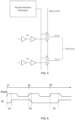
- FIG. 4 shows a MUX-based circuit diagram for IC failure prediction.
- a multiplexer (Mux_sel) is used to select one or more of the data-paths, and then detect a delay timing fingerprint as described herein.
- the advantage with the MUX-based MFPC is that the one signal is selected for delay timing at a time, so failure may be detected with less data (such as with a dedicated analysis circuit on the IC).
- a hybrid MUX/XOR based MFPC may be used that combine some of the advantages from each type of MFPC.
- FIG. 5 shows a circuit diagram for anti-IC aging mode.
- the figure shows an anti-aging technique that deactivates the XOR circuit when the MFPC circuit is not enabled i.e. the MFPC clock is gated.
- the circuit is disabled, a constant logic delay will increase the circuit degradation, such as due to NBTI effects.
- the XOR circuit is toggled whenever the MFPC clock is gated.
- each of the signals is monitored separately for margin degradation.
- FIG. 5 is just one example of alternative embodiments of circuit corrections that may be performed to compensate for the degradation and/or aging of the IC circuit. Many other example circuits may be used.
- phase paths may be expand to other types of logic paths/signals, path lengths, and different types of generating and sampling electronic elements.
- phase paths may be detect hold-failure (min-delay) that is caused by a delay degradation in the clock path.
- a new delay-path (such as D4) is located between the clock of FF1 and FF2such that the D4 delay value delays the clock of FF2.
- the MFPC may be always on or activated by an enable signal.
- an enable signal represents a logical OR of the enable signals corresponding to the group of FFs that are sampled by the MFPC.
- the MFPC may enter into an anti-IC aging mode detection, where a dedicated clock is used to toggle the MFPC to mitigate NBTI aging effects.
- the MFPC may be used as a timing delay margin signature or fingerprint of the IC at first operation. Over time, the MFPC may measure the margin signature at different times to analyze and detect the time gradient of the IC degradation/aging. Different gradient functions may be related to different types of defects and degradation modes.
- the signature comprises multiple, overlapping delay margins, and a several critical timing delay margins are identified as having different time gradients each, and each is separately analyzed to predict a future IC failure.
- nonlinear, spatiotemporal correlation methods are used to track multiple timing delay margins simultaneously from a series of signatures or fingerprints, each signature or fingerprint representing a one-dimensional vector of all timing delays overlapped.
- a transformation is performed of multiple one-dimensional vectors to produce a two or more-dimensional data representation.
- An integrated circuit (IC) embodiment using the techniques disclosed herein includes a failure prediction circuit and a system that may alert of an imminent failure before the failure occurs.
- variable delay time may be set in an integer multiple of increments equal to a clock period of the IC divided by a factor (a "signature vector size"), which is preferably from 1 to 100,000.
- the failure prediction circuit is comprised of a pair of storage components (e.g., flip-flops) that both receive a data signal output from a large number of paths of the IC, such as a data-path, memory paths, logic paths, and/or the like.
- the data signal is reduced using Hamming codes, parity codes, other error-correction techniques, and/or the like, before being stored in the two storage components.
- the two storage components differ from each other in data signal input timings, clock signal input timings, phase of input signals, input logic thresholds of the data signal, and/or the like.
- a variable timing circuit is used to delay the signal to one of the flip-flops.
- the FPC or MFPC further includes electronic components that determine (a) coincidence or non-coincidence of the outputs from the two storage components, and (b) how close the delay between non-coinciding outputs is to the clock cycle time of the IC.
- the failure prediction circuit increments the input timing, clock signal input timing, or input logic thresholds of one of the storage components, and the coincidence or non-coincidence of the outputs is determined again. This cycle may be repeated with small increments.
- a log is maintained of the relative length of the sensed delay in comparison to the clock cycle time, as well as of the storage components increment used.
- Analysis such as trend detection, combinatorial analysis, machine learning, regression analysis, anomaly detection, and/or the like, may be performed on the logged data, to estimate when the ICs degradation may reach a time when the IC fails, such as when the shortest logical path delay exceeds the subsequent clock cycle time.
- This measurement and/or estimation may be utilized in a number of ways.
- An alert may be issued to the user of the system where the IC is implemented, indicating either the margin (how close the delay is to the IC's clock cycle time) or the estimated failure time.
- the agent may instruct an operational change of the IC, such as clock speed or voltage reduction, which may postpone the failure and prolong the IC's lifespan.
- the input signals are compressed to generate a Hamming code (compressed into the Hamming space).
- the Hamming-code may be used for higher-order of error detection, correction, and/or prediction process.
- an XOR-based circuit is used to combine all data-path signals into two unified signal path that implements a modulo-4 logic operation.
- Other types of compression (source) code may be used additionally or as an alternative.
- the signal path combiner (or at least one of the signal path combiners) comprises at least one of a logical XOR combiner (as shown in FIG. 3 or FIG. 3A ), a Hamming parity combiner, and a multiplexer.
- the technique may be expanded to other types of logic-paths and sampling sequential elements, for example:
- the failure prediction circuit may be always on or may be activated by an enable signal that represents a logic-OR of the signals of a data-path. When the enable is low, the failure prediction circuit uses a dedicated clock to toggle the circuit to mitigate aging effects.
- Integrated circuits may implement a large number of synchronous and timing sensitive logic circuits.
- a timing violation occurs, and the violation may affect the functionality of the circuit.
- the physical degradation may be caused by aging effects, or due to defects that developed during use.
- the failure prediction circuit tracks the logic delay margin over time, and may predict a failure due to physical delay degradation.
- the mitigation circuit is at least one circuit from the group consisting of: a notification circuit (for example, as configured to produce notification 206 or 213); a timing delay measurement (or estimation) circuit (for example, for providing a timing delay output); a data transmission circuit; an IC anti-aging compensation circuit (for instance, as discussed with reference to FIG. 5 above); and a failure analysis circuit.
- the mitigation circuit is a data transmission circuit
- the computerized server may be electrically connected to a computerized server.
- the computerized server is advantageously configured to receive multiple instances of the comparison data signal (for example in respect of different times and/or different data sources).
- the computerized server may thereby perform a failure prediction analysis of the comparison data signals.
- it may send a notification to a mitigation module (such as an IC anti-aging compensation circuit) when the failure prediction analysis predicts failure of the IC within a predefined time.
- a mitigation module such as an IC anti-aging compensation circuit
- At least some of the comparison data signals may be generated at multiple values of the variable delay time and/or at least some of the comparison data signals may be generated from multiple instances of at least one value from multiple values of the variable delay time.
- the failure prediction analysis comprises at least one of a machine learning analysis, a trend analysis, a multiple object tracking analysis, and a multivariant analysis.
- the failure prediction analysis comprises receiving comparison data signals and/or failure prediction analysis results from multiple different ICs.
- the failure prediction circuit beneficially continuously monitors a large number of logic circuits, such as signals of a data-path on the output of a functional unit of an IC, using small IC area and power.
- a computer algorithm may be used to determine the population of the failure prediction circuits within a unit per a pre-defined coverage. It may use design-data such as memory-circuits and flip-flop-circuits within the unit. The computer algorithm may also be used to automatically locate the FPC or MFPC circuits per the unit clock-gate signals and to automatically set the input-signal-size per FPC or MFPC for optimal performance (maximum instance coverage with minimum number of FPC or MFPC circuits).
- the delays within the failure prediction circuit may be calibrated. This may be done in order to have a very fast correlation path to the design data and to provide accurate margin results at time zero (during test).
- One calibration methodology may use Pre-Si estimator functions that are based on on-die sensors (agents) in Post-Si to translate the FPC or MFPC circuit measured margin in Pre-Si to the worst case margin of the monitored endpoints (FFs) margins.
- this may be considered to include measuring or estimating a timing delay for the IC (particularly at initial or time-zero operation), based on the comparison data signal provided to the mitigation circuit.
- the timing delay may be based on a plurality of comparison outputs (which may be in a single comparison data signal or a plurality of comparison data signals), for example determined by repeating the steps of combining, delaying and comparing for each of a plurality of delay times.
- the delay through X1..Xn + XorlA + Xor2A is balanced to a delay applied to the clock used for the output flip-flop (D3) in order to make the calibration shift minimal.
- the timing margin data of a large-scale logic circuit within a unit or a die that was extracted at time-zero may be tracked and compared over time.
- the tracking may detect and/or predict a timing failure due to change in the delay and/or aging degradation of the IC.
- FIG. 11 shows a Margin-Map diagram of a unit. This is an example of a unit margin map that represents the unit margin finger-print at the beginning of life (the margin is represented by an equivalent buffer-delay).
- the signature may be used for chip outlier detection/screening.
- a specific IC is given a unique identity and the signature is compared to other ICs, which allows detecting anomalies in a large manufacturing scale.
- the margin-map can be tracked over time to measure the margin signature at different times to analyze and detect the time gradient of the IC degradation or aging. Different gradient functions may be related to different types of defects and degradation modes.
- the margin data of a die can be collected and used for die-classification and anomaly-detection processes. This is done by collecting the margin data of a unit within a die and use ML algorithms to build an estimator function that are based on on-die sensors. More details are described in US provisional patent application No. 62/675,986 Entitled “INTEGRATED CIRCUIT PROFILING AND ANOMALY DETECTION", FILED April 16, 2018 , the contents of which incorporated herein by reference in their entirety.
- the margin data can be analyzed per a specific running application to generate an application-based frequency/power binning.
- Theorem 1 At time t,
- Case B We represent XOR1 by 3 XORs: XORa, XORb and XORc. Their inputs are as follows:
- the output of XORc (which is actually the output of XOR1) may be changed at the time window ( T - D 2 , T ] with some probability, and hence the output of XOR2 may be 1'.
- the probability P in which the output of XOR2 is 1' is the probability in which the output of XORa is changed in two sequential cycles. That probability is 2 q out (1 - q out ) where q out is the probability that the output of XORa is 0'.
- Lemma 1 Let a and b stand for signals for which the probabilities for 0' are q a and q b respectively. Then, q c (1 - q c ) ⁇ max q a (1 - q a ), q b (1 - q b ), where q c stands for the probability that the output of XOR ( a, b ) is 0'.
- the MUX-based MFPC may be considered a special case of the XOR-based MFPC.
- the mathematical proof below of the XOR-based version holds for the MUX-based version.
- FIG. 6 shows a timing diagram of a signal delay for IC failure prediction.
- FIG. 6 shows an event-based simulation description, with simulation settings:
- D2 value XOR2 output transitions may be counted, and the number of counts is plotted vs. the margin timing value threshold.
- FIG. 7 shows a graph of errors versus cycle time for a first experiment.
- the solid line represents the MFPC output at time-zero (without degradation), and the dashed line represents the MFPC output after degradation.
- the minimum margin was equal to 25 time-units, such as [100-75], and MaxD2 at failure was 75 time-units.
- the margin of one path was reduced by 15 time units (margin is distributed uniformly, and the max value was moved by 15 time units), the MFPC detects the change in the margin.
- the minimum margin was equal to 10 time-units, such as [100-75-15], and MaxD2 at failure was 90 time-units.
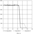
- FIG. 8 shows a graph of errors versus cycle time for a second experiment.
- the solid line represents the MFPC output at time-zero (no degradation), and the dashed line represent the MFPC output after degradation.
- the minimum margin of all the paths with [ Xi+di > 70] (margin ⁇ 30) was increased by 15 time-units, and this was performed for 5 signal paths.
- the minimum margin was equal to 25 time-units, such as [100-75], and MaxD2 at failure was 75 time-units.
- the MFPC detects the change in the margin, where the minimum margin was equal to 10 time-units, such as [100-75-15], and MaxD2 at failure was 90 time-units.
- the counts at XOR2 output are gradually reduced to zero. The probability of failure was increased with the number of paths.
- FIG. 9 shows a timing diagram of two signal delays for IC failure prediction.
- the multiple signals are switched simultaneously, with equal delay and logic value at each cycle.
- the duplicate signals are implemented with the smallest margin.
- the maximum value of [ Xi + di ] is shown, where delay of the duplicated paths was increased by 15 time-units. Both paths implement the same degradation.
- FIG. 10 shows a graph of errors versus cycle time for a third experiment.
- the solid line represents no degradation
- the dashed line (similar to the solid line) represents a first degradation scenario ( Fig 9 upper line)
- the dot-dashed line represents a second degradation scenario in which the delay of one of the duplicated paths was increased by an additional 5 time-units ( Fig 9 lower line).
- the two paths are logically identical, but implement different timing degradations.
- the minimum margin was equal to 25 time-units, such as [100-75].
- the system may not detect the change in the margin.
- MaxD2 at failure equals 75 time-units for both scenarios.
- the system detects the change in the margin. MaxD2 at failure was 95 time-units.
- range format is merely for convenience and brevity and should not be construed as an inflexible limitation on the scope of the invention. Accordingly, the description of a range should be considered to have specifically disclosed all the possible subranges as well as individual numerical values within that range. For example, description of a range such as from 1 to 6 should be considered to have specifically disclosed subranges such as from 1 to 3, from 1 to 4, from 1 to 5, from 2 to 4, from 2 to 6, from 3 to 6 etc., as well as individual numbers within that range, for example, 1, 2, 3, 4, 5, and 6. This applies regardless of the breadth of the range.
- nouns as common nouns, proper nouns, named nouns, and the/or like is not intended to imply that embodiments of the invention are limited to a single embodiment, and many configurations of the disclosed components can be used to describe some embodiments of the invention, while other configurations may be derived from these embodiments in different configurations.
- circuits and physical structures are generally presumed, it is well recognized that in modern semiconductor design and fabrication, physical structures and circuits may be embodied in computer readable descriptive form suitable for use in subsequent design, test or fabrication stages as well as in resultant fabricated semiconductor integrated circuits. Accordingly, claims directed to traditional circuits or structures may, consistent with particular language thereof, read upon computer readable encodings and representations of same, whether embodied in media or combined with suitable reader facilities to allow fabrication, test, or design refinement of the corresponding circuits and/or structures. Structures and functionality presented as discrete components in the exemplary configurations may be implemented as a combined structure or component.
- a computer readable medium includes at least disk, tape, or other magnetic, optical, semiconductor (e.g., flash memory cards, ROM), or electronic medium and a network, wireline, wireless or other communications medium.
- Embodiments of the present invention may be used to fabricate, produce, and/or assemble integrated circuits and/or products based on integrated circuits.
- each block in the flowchart or block diagrams may represent a module, segment, or portion of instructions, which comprises one or more executable instructions for implementing the specified logical function(s).
- the functions noted in the block may occur out of the order noted in the figures.
- two blocks shown in succession may, in fact, be executed substantially concurrently, or the blocks may sometimes be executed in the reverse order, depending upon the functionality involved.
Landscapes
- Engineering & Computer Science (AREA)
- Physics & Mathematics (AREA)
- General Physics & Mathematics (AREA)
- General Engineering & Computer Science (AREA)
- Environmental & Geological Engineering (AREA)
- Health & Medical Sciences (AREA)
- Toxicology (AREA)
- Computer Hardware Design (AREA)
- Microelectronics & Electronic Packaging (AREA)
- Tests Of Electronic Circuits (AREA)
- Semiconductor Integrated Circuits (AREA)
- Testing Of Individual Semiconductor Devices (AREA)
Abstract
Description
- This application claims the benefit of priority of
U.S. Provisional Patent Application No. 62/586,423, filed November 15, 2017 - The invention relates to the field of integrated circuits.
- Integrated circuits (ICs) may include analog and digital electronic circuits on a flat semiconductor substrate, such as a silicon wafer. Microscopic transistors are printed onto the substrate using photolithography techniques to produce complex circuits of billions of transistors in a very small area, making modern electronic circuit design using ICs both low cost and high performance. ICs are produced in assembly lines of factories, termed foundries, that have commoditized the production of ICs, such as complementary metal-oxide-semiconductor (CMOS) ICs. Digital ICs contain billions of transistors arranged in functional and/or logical units on the wafer, with data-paths interconnecting the functional units that transfer data values between the functional units. As used herein, the term "data-path" means a parallel series of electronic connections, or paths, for transferring data signals between functional/logical units of an IC, and each data-path may include a specific number of bit paths, such as 64, 128, 256, ort the like. During the IC design process, the timing of the functional units is arranged so that each functional unit may usually complete the required processing of that unit within a single clock cycle. A safety factor may be used to account for manufacturing differences of individual ICs and possible changes, such as degradations, over the planned lifetime of the IC.
- The degrading of an IC's transistors over time is termed aging. For example, the degradation of transistors over time leads slowly to decreased switching speeds, and may even result in outright circuit failures, when they exceed the design safety factors. Usually, the design process incorporates these delays into the design such that the ICs will not fail during their normal lifetime, but environmental and usage conditions (such as heat, voltage, current, humidity, and/or the like) may accelerate the aging process.
- IC transistors, such as bipolar transistors, metal-oxide semiconductor field-effect transistors (MOSFETs), and/or the like, may be used in digital ICs and may function as electrical switches. For example, a MOSFET may have four terminals, such as the body, the gate, the source, and the drain, yet typically the source and body are electrically connected. The voltage applied to the gate may determine the amount of current that flows between the source and drain. A thin layer of dielectric material electrically insulates the gate, and the electric field applied across the gate may alter the conductivity of the underlying semiconductor channel between the source and drain.
- With use, charge carriers (such as electrons for negative, or n-channel, MOSFETs, or holes for positive, or p-channel, MOSFETs) that have more energy than the average charge carrier may stray out of the conductive channel between the source and drain, and become trapped in the insulating dielectric. This process, termed hot-carrier injection (HCI), may eventually build up electric charge within the dielectric layer, and thus increase the voltage needed to operate the transistor. As the threshold voltage increases, the transistor switching delay may become larger.
- Another aging mechanism occurs when a voltage is applied to the gate, a phenomenon termed bias temperature instability (BTI). BTI may cause a buildup of charge in the dielectric, among other issues, though, some of this effect spontaneously disappears after that gate voltage is removed. This recovery occurs within a few microseconds, making it difficult to observe when a transistor is stressed and then the resulting effects are measured only after the stress is removed.
- Another aging mechanism comes into play when a voltage applied to the gate may create electrically active defects, known as traps, within the dielectric. When traps become too numerous, these charge traps may join and form an outright short circuit between the gate and the current channel. This kind of failure is termed oxide breakdown, or time-dependent dielectric breakdown. Unlike the other aging mechanisms, which cause a gradual decline in performance, the breakdown of the dielectric may lead to a catastrophic failure of the transistor, causing the IC to malfunction.
- Additionally, a phenomenon called electromigration may damage the copper or aluminum connections that tie transistors together or link them to the outside world. Electromigration may occur when a surge of current knocks metal atoms loose from the electrical connections, and may cause them to flow with the electrons. This depletes the metal of some atoms upstream, while causing a buildup of metal downstream. The upstream thinning of the metal increases the electrical resistance of the connection, sometimes becoming an open circuit. The downstream deposition may cause the metal to bulge out of its designated track.
- Another reliability related issue in ICs is a phenomenon called stress migration. This is used to describe the flow of metal atoms under the influence of mechanical stress.
- Additionally, any defect, such as un-modeled phenomenon, random manufacturing defects, and/or the like, may cause a timing degradation of a signal path over time. Some defects may not appear during testing, verification, initial operation, and/or the like, for example, the die/IC/product may pass all the screening procedures at the testing stage. For example, a via that includes a manufacturing defects, such as less that complete metal coverage, will increase its resistance over time and at some point, causes a timing failure of a logic path. For example, random manufacturing defects may appear anywhere on the IC, and incorporate a large variety of types and levels of defects, so designs may not be able to incorporate safety factors to mitigate these defects. On the other hand, aspects of embodiments of the disclosed techniques may be able to predict the failure of each individual IC based on fingerprint sampling at appropriate IC pathways, and mitigate the failure by preemptive replacement, corrective and preventative actions, notifications to users, compensations within the IC to increase time lifetime, and/or the like.
- The foregoing examples of the related art and limitations related therewith are intended to be illustrative and not exclusive. Other limitations of the related art will become apparent to those of skill in the art upon a reading of the specification and a study of the figures.
- The following embodiments and aspects thereof are described and illustrated in conjunction with systems, tools and methods which are meant to be exemplary and illustrative, not limiting in scope.
- There is provided, in accordance with an embodiment, a semiconductor integrated circuit (IC) in accordance with the claims. This may comprise a signal path combiner, comprising a plurality of input paths and an output path. The IC comprises a delay circuit having an input electrically connected to the output path, the delay circuit delaying an input signal by a variable delay time to output a delayed signal path. The IC may comprise a first storage circuit electrically connected to the output path and a second storage circuit electrically connected to the delayed signal path. The IC comprises a comparison circuit that compares outputs of the first and second storage circuits, wherein the comparison circuit comprises a second output path electrically connected to one or more mitigation circuit.
- In some embodiments, the mitigation circuit is one or more circuit from the group consisting of: a notification circuit; a timing delay measurement (or estimation) circuit; a data transmission circuit; an IC anti-aging compensation circuit; and a failure analysis circuit.
- In some embodiments, the signal path combiner is one or more from the group consisting of a logical XOR combiner, a Hamming parity combiner, and multiplexer.
- In some embodiments, the variable delay time is set in an integer multiple of increments equal to a clock period of the IC divided by a signature vector size, and wherein the signature vector size is between 1 and 100,000.
- In some embodiments, the mitigation circuit is a data transmission circuit electrically connected to a computerized server, wherein the computerized server is configured to receive multiple instances of the comparison data signal, perform a failure prediction analysis of the comparison data signals, and send a notification a mitigation module when the failure prediction analysis predicts failure of the IC within a predefined time.
- In some embodiments, at least some of the comparison data signals are generated at multiple values of the variable delay time.
- In some embodiments, at least some of the comparison data signals are generated from multiple instances of one or more value from multiple values of the variable delay time.
- In some embodiments, the failure prediction analysis comprises one or more of a machine learning analysis, a trend analysis, a multiple object tracking analysis, and a multivariant analysis.
- In some embodiments, the failure prediction analysis comprises receiving comparison data signals from multiple different ICs.
- In some embodiments, the failure prediction analysis comprises receiving failure prediction analysis results from multiple different ICs.
- In a further aspect, which may be combinable with any embodiment described herein, there is provided a semiconductor integrated circuit (IC) comprising: a signal path combiner, comprising a plurality of input paths and an output, the output being based on a combination of respective signals received on each of the input paths; a delay circuit having an input electrically connected to the signal path combiner output, the delay circuit delaying an input signal by a variable delay time to output a delayed signal; and a comparison circuit arranged to provide a comparison output based on a comparison of the signal path combiner output and the delayed signal, wherein the comparison output is provided in a comparison data signal to at least one mitigation circuit.
- In some embodiments, the mitigation circuit is at least one circuit from the group consisting of: a notification circuit; a timing delay measurement circuit; a data transmission circuit; an IC anti-aging compensation circuit; and a failure analysis circuit.
- Optionally, the signal path combiner is at least one from the group consisting of a logical XOR combiner, a Hamming parity combiner, and multiplexer.
- In an embodiment, the IC further comprises: a first internal storage circuit, electrically connected to the signal path combiner output and arranged to provide the stored signal path combiner output as a first input to the comparison circuit; and a second internal storage circuit, electrically connected to the delayed signal and arranged to provide the delayed signal as a second input to the comparison circuit.
- In certain embodiments, the signal path combiner is a first signal path combiner arranged to receive a plurality of signals from a first data source and the comparison circuit is a first comparison circuit. Then, the IC may further comprise: a second signal path combiner, comprising a plurality of input paths and an output, the second signal path combiner output being based on a combination of respective signals received on each of the input paths, the signals being received from a second data source; a multiplexer, configured to receive the first signal path combiner output, the second signal path combiner output and a selection signal and to selectively output the first signal path combiner output or the second signal path combiner output based on the selection signal, the output of the multiplexer being provided as the input to the delay circuit; a second comparison circuit arranged to provide a second comparison output based on a comparison of the second signal path combiner output and the delayed signal; and an OR gate arranged to receive as inputs the first comparison output and the second comparison output and to provide an output as the comparison data signal to the at least one mitigation circuit.
- The IC optionally, further comprises: a first comparison storage circuit, arranged to receive the first comparison output and controlled by a first clock signal; a second comparison storage circuit, arranged to receive the second comparison output and controlled by a second clock signal; and wherein the first comparison storage circuit is arranged to provide the first comparison output as a first input to the OR gate and the second comparison storage circuit is arranged to provide the second comparison output as a second input to the OR gate.
- In some embodiments the variable delay time is set in an integer multiple of increments equal to a clock period of the IC divided by a signature vector size, and wherein the signature vector size is between 1 and 100,000.
- In embodiments, the mitigation circuit is a data transmission circuit electrically connected to a computerized server, wherein the computerized server is configured to receive multiple instances of the comparison data signal, perform a failure prediction analysis of the comparison data signals, and send a notification to a mitigation module when the failure prediction analysis predicts failure of the IC within a predefined time. Optionally, at least some of the comparison data signals are generated at multiple values of the variable delay time. Preferably, at least some of the comparison data signals are generated from multiple instances of at least one value from multiple values of the variable delay time.
- In certain embodiments, the failure prediction analysis comprises at least one of a machine learning analysis, a trend analysis, a multiple object tracking analysis, and a multivariant analysis.
- In embodiments, the failure prediction analysis comprises receiving comparison data signals from multiple different ICs.
- In some embodiments, the failure prediction analysis comprises receiving failure prediction analysis results from multiple different ICs.
- In some embodiments, each of the plurality of input paths of the signal path combiner is configured to receive one of: a signal from a respective data source in the IC; a signal from a memory circuit; and a signal from one of a plurality of logic circuits grouped by a clock enable.
- In another aspect (combinable with any other embodiment described herein), there may be considered a method for using a semiconductor integrated circuit (IC), the method comprising: combining respective signals received on each of a plurality of input paths at a signal path combiner to provide an output; delaying the signal path combiner output by a variable delay time at a delay circuit to output a delayed signal; and comparing the signal path combiner output and the delayed signal to provide a comparison output and providing the comparison output in a comparison data signal to at least one mitigation circuit.
- In some embodiments, the mitigation circuit is at least one circuit from the group consisting of: a notification circuit; a timing delay measurement circuit; a data transmission circuit; an IC anti-aging compensation circuit; and a failure analysis circuit.
- In embodiments, the signal path combiner is at least one from the group consisting of a logical XOR combiner, a Hamming parity combiner, and multiplexer.
- Optionally, the method further comprises: storing the signal path combiner output at a first internal storage circuit and providing the stored signal path combiner output from the first internal storage circuit as a first input to the comparison circuit; and storing the delayed signal at a second internal storage circuit and providing the delayed signal from the second internal storage circuit as a second input to the comparison circuit.
- In certain embodiments, the signal path combiner is a first signal path combiner that receives a plurality of signals from a first data source and wherein the comparison circuit is a first comparison circuit. Then, the method may further comprise: combining respective signals received on each of a plurality of input paths at a second signal path combiner to provide an output, the signals being received from a second data source; receiving the first signal path combiner output, the second signal path combiner output and a selection signal at a multiplexer and selectively outputting the first signal path combiner output or the second signal path combiner output based on the selection signal, the output of the multiplexer being provided as the input to the delay circuit such that the step of delaying comprises delaying the first signal path combiner output or the second signal path combiner output by the variable delay time at the delay circuit to output the delayed signal; comparing the second signal path combiner output and the delayed signal to provide a second comparison output; and receiving at an OR gate, the first comparison output and the second comparison output as inputs and outputting the comparison data signal as an output from the OR gate to the at least one mitigation circuit.
- In some embodiments, the method further comprises: receiving the first comparison output at a first comparison storage circuit controlled by a first clock signal; receiving the second comparison output at a second comparison storage circuit controlled by a second clock signal; providing the first comparison output from the first comparison storage circuit as a first input to the OR gate; and providing the second comparison output from the second comparison storage circuit as a second input to the OR gate.
- In embodiments, the variable delay time is set in an integer multiple of increments equal to a clock period of the IC divided by a factor from 1 to 100,000.
- In some embodiments, the mitigation circuit is a data transmission circuit electrically connected to a computerized server, the method further comprising: receiving multiple instances of the comparison data signal at the computerized server; performing a failure prediction analysis of the comparison data signals at the computerized server; sending a notification from the computerized server to a mitigation module when the failure prediction analysis predicts failure of the IC within a predefined time. Optionally, at least some of the comparison data signals are generated at multiple values of the variable delay time. Preferably, at least some of the comparison data signals are generated from multiple instances of at least one value from multiple values of the variable delay time.
- In some embodiments, the failure prediction analysis comprises at least one of a machine learning analysis, a trend analysis, a multiple object tracking analysis, and a multivariant analysis.
- In certain embodiments, the failure prediction analysis comprises receiving comparison data signals from multiple different ICs.
- In embodiments, the failure prediction analysis comprises receiving failure prediction analysis results from multiple different ICs.
- Optionally, each of the plurality of input paths of the signal path combiner is configured to receive one of: a signal from a respective data source in the IC; a signal from a memory circuit; and a signal from one of a plurality of logic circuits grouped by a clock enable.
- In embodiments, the method is performed at an initial operation of the IC. Then, the method may further comprise: measuring a timing delay for the IC, based on the comparison data signal provided to the mitigation circuit.
- In some embodiments, the method further comprises: repeating the steps of combining, delaying and comparing for each of a plurality of delay times, in order to provide a plurality of comparison outputs; and determining an identifying characteristic for the IC based on the plurality of comparison outputs. Optionally, the method further comprises: tracking changes in the identifying characteristic for the IC over time.
- In addition to the exemplary aspects and embodiments described above, further aspects and embodiments will become apparent by reference to the figures and by study of the following detailed description.
- 1. A semiconductor integrated circuit (IC) comprising:
- a signal path combiner, comprising a plurality of input paths and an output, the output being based on a combination of respective signals received on each of the input paths;
- a delay circuit having an input electrically connected to the signal path combiner output, the delay circuit delaying an input signal by a variable delay time to output a delayed signal; and
- a comparison circuit arranged to provide a comparison output based on a comparison of the signal path combiner output and the delayed signal, wherein the comparison output is provided in a comparison data signal to at least one mitigation circuit.
- 2. The IC of
clause 1, wherein the mitigation circuit is at least one circuit from the group consisting of:- (i) a notification circuit;
- (ii) a timing delay measurement circuit;
- (iii) a data transmission circuit;
- (iv) an IC anti-aging compensation circuit; and
- (v) a failure analysis circuit.
- 3. The IC of
clause 1 orclause 2, wherein the signal path combiner is at least one from the group consisting of a logical XOR combiner, a Hamming parity combiner, and multiplexer. - 4. The IC of any one of
clauses 1 to 3, further comprising:- a first internal storage circuit, electrically connected to the signal path combiner output and arranged to provide the stored signal path combiner output as a first input to the comparison circuit; and
- a second internal storage circuit, electrically connected to the delayed signal and arranged to provide the delayed signal as a second input to the comparison circuit.
- 5. The IC of any one of
clauses 1 to 4, wherein the signal path combiner is a first signal path combiner arranged to receive a plurality of signals from a first data source and wherein the comparison circuit is a first comparison circuit, the IC further comprising:- a second signal path combiner, comprising a plurality of input paths and an output, the second signal path combiner output being based on a combination of respective signals received on each of the input paths, the signals being received from a second data source;
- a multiplexer, configured to receive the first signal path combiner output, the second signal path combiner output and a selection signal and to selectively output the first signal path combiner output or the second signal path combiner output based on the selection signal, the output of the multiplexer being provided as the input to the delay circuit;
- a second comparison circuit arranged to provide a second comparison output based on a comparison of the second signal path combiner output and the delayed signal; and
- an OR gate arranged to receive as inputs the first comparison output and the second comparison output and to provide an output as the comparison data signal to the at least one mitigation circuit.
- 6. The IC of clause 5, further comprising:
- a first comparison storage circuit, arranged to receive the first comparison output and controlled by a first clock signal;
- a second comparison storage circuit, arranged to receive the second comparison output and controlled by a second clock signal; and
- wherein the first comparison storage circuit is arranged to provide the first comparison output as a first input to the OR gate and the second comparison storage circuit is arranged to provide the second comparison output as a second input to the OR gate.
- 7. The IC of any one of
clauses 1 to 4, wherein the variable delay time is set in an integer multiple of increments equal to a clock period of the IC divided by a signature vector size, and wherein the signature vector size is between 1 and 100,000. - 8. The IC of any one of
clauses 1 to 7, wherein the mitigation circuit is a data transmission circuit electrically connected to a computerized server, wherein the computerized server is configured to receive multiple instances of the comparison data signal, perform a failure prediction analysis of the comparison data signals, and send a notification to a mitigation module when the failure prediction analysis predicts failure of the IC within a predefined time. - 9. The IC of clause 8, wherein at least some of the comparison data signals are generated at multiple values of the variable delay time.
- 10. The IC of clause 9, wherein at least some of the comparison data signals are generated from multiple instances of at least one value from multiple values of the variable delay time.
- 11. The IC of any one of clauses 8 to 10, wherein the failure prediction analysis comprises at least one of a machine learning analysis, a trend analysis, a multiple object tracking analysis, and a multivariant analysis.
- 12. The IC of any one of clauses 8 to 11, wherein the failure prediction analysis comprises receiving comparison data signals from multiple different ICs.
- 13. The IC of any one of clauses 8 to 12, wherein the failure prediction analysis comprises receiving failure prediction analysis results from multiple different ICs.
- 14. The IC of any one of
clauses 1 to 13, wherein each of the plurality of input paths of the signal path combiner is configured to receive one of: a signal from a respective data source in the IC; a signal from a memory circuit; and a signal from one of a plurality of logic circuits grouped by a clock enable. - 15. A method for using a semiconductor integrated circuit (IC), the method comprising:
- combining respective signals received on each of a plurality of input paths at a signal path combiner to provide an output;
- delaying the signal path combiner output by a variable delay time at a delay circuit to output a delayed signal; and
- comparing the signal path combiner output and the delayed signal to provide a comparison output and providing the comparison output in a comparison data signal to at least one mitigation circuit.
- 16. The method of clause 15, wherein the mitigation circuit is at least one circuit from the group consisting of:
- (i) a notification circuit;
- (ii) a timing delay measurement circuit;
- (iii) a data transmission circuit;
- (iv) an IC anti-aging compensation circuit; and
- (v) a failure analysis circuit.
- 17. The method of clause 15 or clause 16, wherein the signal path combiner is at least one from the group consisting of a logical XOR combiner, a Hamming parity combiner, and multiplexer.
- 18. The method of any one of clauses 15 to 17, further comprising:
- storing the signal path combiner output at a first internal storage circuit and providing the stored signal path combiner output from the first internal storage circuit as a first input to the comparison circuit; and
- storing the delayed signal at a second internal storage circuit and providing the delayed signal from the second internal storage circuit as a second input to the comparison circuit.
- 19. The method of any one of clauses 15 to 18, wherein the signal path combiner is a first signal path combiner that receives a plurality of signals from a first data source and wherein the comparison circuit is a first comparison circuit, the method further comprising:
- combining respective signals received on each of a plurality of input paths at a second signal path combiner to provide an output, the signals being received from a second data source;
- receiving the first signal path combiner output, the second signal path combiner output and a selection signal at a multiplexer and selectively outputting the first signal path combiner output or the second signal path combiner output based on the selection signal, the output of the multiplexer being provided as the input to the delay circuit such that the step of delaying comprises delaying the first signal path combiner output or the second signal path combiner output by the variable delay time at the delay circuit to output the delayed signal;
- comparing the second signal path combiner output and the delayed signal to provide a second comparison output; and
- receiving at an OR gate, the first comparison output and the second comparison output as inputs and outputting the comparison data signal as an output from the OR gate to the at least one mitigation circuit.
- 20. The method of clause 19, further comprising:
- receiving the first comparison output at a first comparison storage circuit controlled by a first clock signal;
- receiving the second comparison output at a second comparison storage circuit controlled by a second clock signal;
- providing the first comparison output from the first comparison storage circuit as a first input to the OR gate; and
- providing the second comparison output from the second comparison storage circuit as a second input to the OR gate.
- 21. The method of any one of clauses 15 or
clause 20, wherein the variable delay time is set in an integer multiple of increments equal to a clock period of the IC divided by a factor from 1 to 100,000. - 22. The method of any one of clauses 15 to 21, wherein the mitigation circuit is a data transmission circuit electrically connected to a computerized server, the method further comprising: receiving multiple instances of the comparison data signal at the computerized server; performing a failure prediction analysis of the comparison data signals at the computerized server; sending a notification from the computerized server to a mitigation module when the failure prediction analysis predicts failure of the IC within a predefined time.
- 23. The method of clause 22, wherein at least some of the comparison data signals are generated at multiple values of the variable delay time.
- 24. The method of clause 23, wherein at least some of the comparison data signals are generated from multiple instances of at least one value from multiple values of the variable delay time.
- 25. The method of any one of clauses 22 to 24, wherein the failure prediction analysis comprises at least one of a machine learning analysis, a trend analysis, a multiple object tracking analysis, and a multivariant analysis.
- 26. The method of any one of clauses 22 to 25, wherein the failure prediction analysis comprises receiving comparison data signals from multiple different ICs.
- 27. The method of any one of clauses 22 to 26, wherein the failure prediction analysis comprises receiving failure prediction analysis results from multiple different ICs.
- 28. The method of any one of clauses 15 to 27, wherein each of the plurality of input paths of the signal path combiner is configured to receive one of: a signal from a respective data source in the IC; a signal from a memory circuit; and a signal from one of a plurality of logic circuits grouped by a clock enable.
- 29. The method of any one of clauses 15 to 28, wherein the method is performed at an initial operation of the IC, the method further comprising:
measuring a timing delay for the IC, based on the comparison data signal provided to the mitigation circuit. - 30. The method of any one of clauses 15 to 29, further comprising:
- repeating the steps of combining, delaying and comparing for each of a plurality of delay times, in order to provide a plurality of comparison outputs; and
- determining an identifying characteristic for the IC based on the plurality of comparison outputs.
- 31. The method of clause 30, further comprising:
tracking changes in the identifying characteristic for the IC over time. - Exemplary embodiments are illustrated in referenced figures. Dimensions of components and features shown in the figures are generally chosen for convenience and clarity of presentation and are not necessarily shown to scale. The figures are listed below.
-
FIG. 1 shows schematically a computerized system for IC margin measurement and failure prediction; -
FIG. 2 shows flowcharts of methods for IC margin measurement and failure prediction; -
FIG. 3 ,FIG 3A and FIG. 3B show respective XOR-based circuit diagrams for IC margin measurement and failure prediction; -
FIG. 4 shows a MUX-based circuit diagram for IC margin measurement and failure prediction; -
FIG. 5 shows a circuit diagram for anti-IC aging mode; -
FIG. 6 shows a timing diagram of a signal delay for IC margin measurement and failure prediction; -
FIG. 7 shows a graph of errors versus cycle time for a first experiment; -
FIG. 8 shows a graph of errors versus cycle time for a second experiment; -
FIG. 9 shows a timing diagram of two signal delays for IC margin measurement and failure prediction; -
FIG. 10 shows a graph of errors versus cycle time for a third experiment; and -
FIG. 11 shows a Margin-Map diagram of a unit. - Disclosed herein are methods and devices for determining and predicting a future failure of the individual integrated circuit. Also disclosed is a timing delay margin measurement circuit for an IC, from its first operation and/or over time (for example, during any time period from or subsequent to its first operation). A dedicated circuit (which may be detector), such as a failure prediction circuit (FPC) or a margin measurement and failure prediction circuit (MFPC), is placed at selected points along one or more data-paths in a digital integrated circuit (such as one or more FPC or MFPC per data-path), where each dedicated circuit combines multiple individual data paths into a fewer number of test paths. By splitting each test signal into two, and applying a delay circuit to one of the split signal paths, a fingerprint or signature of the delays of each path of the data-path may be acquired during each clock cycle of the functional unit. As used herein, the term "fingerprint" and/or "signature" mean the profile of signal strengths, such as a vector, series, and/or the like, resulting from a measurement of timing delay margins of a combination of signals of a data-path. As used herein, the term "margin" refers to the timing delay of an individual data signal of the data-path. For each clock cycle of the functional unit the output data-path may have a different data value. Thus, during each clock cycle, a different combination of the logical paths within the functional unit may be tested, producing a different fingerprint. By collecting a large number of fingerprints over time, a dataset of fingerprints may be analyzed. The analysis of the fingerprint datasets may determine the performance and/or predict future failure of the individual IC.
- In general terms, there may be considered a semiconductor integrated circuit (IC) comprising: a signal path combiner, comprising a plurality of input paths (for example to receive signals on a data source or data-path, from a memory circuit and/or from logic circuits grouped by a clock enable) and an output, the output being based on a combination of respective signals received on each of the input paths; a delay circuit having an input electrically connected to the signal path combiner output, the delay circuit delaying an input signal by a variable delay time to output a delayed signal; and a comparison circuit arranged to provide a comparison output based on a comparison of the signal path combiner output and the delayed signal, wherein the comparison output is provided in a comparison data signal to at least one mitigation circuit. The combination of the signal path combiner, delay circuit and comparison circuit may provide an FPC or MFPC.
- A method for using such an IC may also be considered (in which using may comprise one of more of operating, analyzing and configuring, for instance). For instance, this may include a method for using a semiconductor integrated circuit (IC). The method may comprise: combining respective signals received on each of a plurality of input paths at a signal path combiner to provide an output; delaying the signal path combiner output by a variable delay time at a delay circuit to output a delayed signal; and comparing the signal path combiner output and the delayed signal to provide a comparison output and providing the comparison output in a comparison data signal to at least one mitigation circuit.
- It may also be considered that the steps of combining, delaying and comparing may be repeated for each of a plurality of delay times. In this way, a plurality of comparison outputs may be provided. An identifying characteristic (i.e. a signature or fingerprint) for the IC may thereby be determined based on the plurality of comparison outputs. By repeating this process over different clock cycles, multiple such fingerprints may be determined. The fingerprints may then be tracked at different times, for example by tracking changes in the fingerprint over time (using intervals at least as long as the length of time taken to determine a single fingerprint and preferably longer).
- Further optional method features corresponding with the steps implemented by any of the features described with reference to the IC may also be provided. Examples of these may be discussed below. Specific embodiments will also be discussed below, but further reference will also be made to generalized senses or terms of the disclosure.
- Note that a data-path is one example of a design style that can be handled by the FPC or MFPC, other examples may be memory circuits (the FPC/MFPC is located at the output of the memory) and other logic circuits that are grouped together with respect to a certain clock enable.
- Optionally, aspects of embodiments described herein may be applied to any reliability problem of IC performance, such as aging, latent defects that manifest in the design and cause degradation, manufacturing differences within/between ICs, manufacturing differences between fabs, and/or the like. The techniques described may find changes in timing delays from any source or cause, predict a future failure before the IC failure causes a device/system failure, and enable corrective and preventive action before the specific IC failure. While reliability issues, such as aging, electro-migration, and/or the like, are used here as examples, the techniques may also be applied to latent defects, such as random defects, systematic defects, unknown defects, and/or the like.
- Optionally, the delay me be changed in small time steps, producing one or more sweeps of time delays, and associated fingerprints at each different time delay. The sweep may be analyzed to determine the operation of the individual IC, predict a future failure of the IC, and/or the like.
- Optionally, one or more datasets (e.g. from signals on the IC) may be analyzed combinatorically to determine the operational delays of each path of the data-path (or equivalent signal path), each logical processing path of the functional unit, and/or the like.
- Optionally, one or more datasets may be analyzed statistically to predict a future failure the IC. For example, an IC degradation trend may be analyzed in one or more delay margins measured using the failure prediction circuit, such as be analyzing a minimum delay margin change over time.
- Optionally, one or more datasets may be analyzed using machine learning to monitor the failure of the IC, predict a future failure of the IC, and/or the like.
- Optionally, one or more datasets may be analyzed to design a future IC.
- Optionally, one or more sweeps may be analyzed combinatorically to determine the operational delays of each path of the data-path, each logical processing path of the functional unit, and/or the like.
- Optionally, one or more sweeps may be analyzed statistically to predict a future failure the IC. For example, a regression analysis of one or more sweeps determines the changes in timing delays, and an extrapolation to a timing delay failure value determines the time to failure.
- Optionally, one or more sweeps may be analyzed using machine learning to monitor the failure of the IC, predict a future failure of the IC, and/or the like.
- Optionally, one or more delay time sweeps may be analyzed to design a future IC, where the future IC is designed to avoid the failures of the previous ICs.
- Optionally, one or more sweeps are analyzed using machine learning at the beginning-of-life of the chip, e.g. the timing delay margins signature or fingerprint of the IC at the beginning-of-life. The signature or fingerprint may be used for chip outlier detection/screening, i.e. a specific IC is given a unique identity and the signature as compared to other ICs that allows detecting anomaly's in a large manufacturing scale.
- Reference is now made to
FIG. 1 andFIG. 2 , which show schematically acomputerized system 100 and flowcharts (200 and 210) of methods, respectively, for IC failure prediction and margin measurement of logic-paths at the IC testing (tester or system level).System 100 comprises anIC 150, acomputer 101A, and adata interface connection 140 connecting the two.IC 150 comprises multiple function units (as at 151, 152, 153, and the like), and data-paths (as at 141, 142A, 142B, 143A, 143B, and the like, which may include synthesized logic) between them.IC 150 comprises margin measurement and failure prediction circuits (MFPCs; as at 131, 132, 133, and the like) for capturing signals from data-paths (as at 142A, 143A, and the like), and determining delay timings of at least some signals form the respective data-path.MFPCs combine 201 signals from the data-path, and test 202 one or more delays of the combined signals.IC 150 comprises a data interface for connecting todata interface connection 140, and sending 202 the delay timings tocomputer 101A. Delay timing data collected for multiple signals of the data-paths and/or for multiple delay values, such as be changing 204 the delay, may be considered the fingerprint of the delay timings. -
Computer 101A comprises one ormore hardware processors 101B, auser interface 120 and a non-transitory, computerreadable storage medium 102. Storage medium comprises program code, such as anMFPC Data Receiver 102A, anIC Aging Analyzer 102B, anIC Failure Predictor 102C, and/or the like, the program code comprising instructions that when executed on hardware processor(s) 101B, cause hardware processor(s) 101B to receive 211 the signal delay data (i.e. fingerprints) using adata interface 110, such as usingMFPC Data Receiver 102A.IC Aging Analyzer 102B analyzes 212 the fingerprints, andIC Failure Predictor 102C notifies 213 an operator of a status, a failure prediction, a preventative action, and or the like, such as usinguser interface 120. - Optionally, the delay timings are analyzed by a circuit (not shown) of
IC 150 to determine when clock and/orlogic modifications 206 onIC 150 improve the lifetime ofIC 150 before failure. Optionally, the delay timings are analyzed by a circuit (not shown) ofIC 150 and anotification 206 is issued of the status or failure prediction. - Optionally, the delay timing fingerprint may be generated at the IC testing (tester or system) to extract the time-zero margin map of the data-paths in a certain unit.
- The fingerprint may be analyzed at a time of initial operation and monitored over the life of the IC to determine when a predicted failure may occur. For example, a defect degradation gradient analysis may determine the future time of a failure of the IC. For example, analyzing the minimum margin of a fingerprint, plotting the minimum margin over time, and extrapolating the plot to a margin delay of zero determines the predicted time of failure.
- Reference is now made to
FIG. 3 , which shows a XOR-based circuit diagram for IC failure prediction. An XOR component (XOR1) combines the signals from a data-path, such as 64, 128, 256, 512, or the like number of signals in to a single signal XOR1_out. XOR1_out is feed into a first flip-flop FF2, and a delay line D2. The delayed XOR1_out is fed into a second flip-flop FF1. FF1 and FF2 are activated by a clock clk_3, and their outputs XOR combined with XOR2. XOR2_out is a logical 1 for each delay where one of XOR1_out and XOR1_out_d2 is logical 1 at time of clk_d1. - Thus, multiple instances of clk_d1 may and/or multiple values of D1 may determine timing delay data of the delay along data-paths of combinatorial (Combinatoric) logic FU1, and thus the fingerprint of timing delays. By analyzing these timing delays over time, the MFPC may detect which of the paths of FU1 is degrading and/or aging fastest, and may cause failure of
IC 150. - The output signal of XOR1 may be considered a compression of the input signals that preserves the minimum timing margin delays of the input signals of the data-path. The output of XOR2 may be logic-1 when the minimum margin of an input signal is smaller than the delay associated with D2. Thus, XOR1 may be a parity checker, i.e. the output is logical 1 when the parity of the input signals is logical 1. Each rising-edge of the compressed signal (XOR1 output) may be associated with a rising edge of one of the input signals. For the simple case in which the minimal timing delay margin is associated with only one input, the last rising or falling transitions of XOR1-output represents the minimal margin. This concept may be proven by a mathematical proof, described hereinbelow, as well as by event-based simulations. For example, special cases may be proved by simulation, where the margin of several signals is smaller than D2, multiple signals switched simultaneously, and/or the like.
- In the general terms considered above, the IC may further comprise: a first internal storage circuit, electrically connected to the signal path combiner output and arranged to provide the stored signal path combiner output as a first input to the comparison circuit; and a second internal storage circuit, electrically connected to the delayed signal and arranged to provide the delayed signal as a second input to the comparison circuit. However, such a configuration is optional, as will now be discussed.
- Reference is now made to
FIG. 3A , which shows a different version of a XOR-based circuit diagram for IC failure prediction, in comparison with that shown inFIG. 3 . The data-path shown inFIG. 3A has essentially the same structure as that shown inFIG. 3 . In this version, a XOR component XOR1a combines the signals from the data-path, such as 64, 128, 256, 512, or the like number of signals, into a single output signal, XOR1aout. XOR1aout is fed as a first a first input to a second XOR circuit XOR2a and in parallel, to a delay-line D2, the output of which provides a second input to the second XOR circuit XOR2a. The delayed output signal from the second XOR circuit XOR2a, XOR2aout, is fed into a flip-flop FF1b. Flip-flop FFlb is activated by a clock (clkla). The second output signal XOR2aout is a logical 1 for each delay where the two inputs of the second XOR circuit XOR2a are at different logic state at time of clkla. - Reference now is made to
FIG.3B , which shows a further different version of a XOR-based circuit diagram for IC failure prediction, in comparison with that shown inFIG. 3 . In this version, two XOR-based failure prediction circuits are provided that use one delay-line circuit. In other words, two data-paths are provided, each of which may be in accordance with that shown inFIG. 3 orFIG. 3A . The first failure prediction circuit comprises: a first XOR component XOR1a that is driven by a set of parallel-input signals from a first data-path (as discussed with reference toFIG. 3 orFIG. 3A above); a second XOR component XOR2a; and a first flip-flop FFlb that is clocked by a first clock signal clkla. The second failure prediction circuit comprises: a third XOR component XORlb that is driven by a set of parallel-input signals from a second data-path (as discussed with reference toFIG. 3 orFIG. 3A above); a fourth XOR component XOR2b; and a second flip-flop FFlb that is clocked by a second clock signal clklb. A common delay-line D2 serves the two failure prediction circuits with a multiplexer mux selecting, in a time-sharing mode, whether the output of the first XOR component XOR1a or the output of the third XOR component XORlb is provided as an input to the common delay-line D2. This is controlled using a selection signal In/out sel. The configuration of each of the two failure prediction circuits is otherwise as shown inFIG. 3A . The output of the first flip-flop FFlb clocked by first clock signal clkla and the output of the second flip-flop FFlb clocked by second clock signal clklb are provided as inputs to an OR gate to generate an output signal MT-out. When the multiplexer mux connects the output of the first XOR component XOR1a to the input of the delay-line D2, output signal MT-out is a logical 1 for each delay where the two inputs of the second XOR component XOR2a are at different logic state at time of the first clock signal clkla. When the multiplexer mux connects the output of the third XOR component XORlb to the input of the delay-line D2, output signal MT-out is a logical 1 for each delay where the two inputs of the fourth XOR component XOR2b are at different logic state at time of second clock signal clklb. - In general terms, it may be further considered that the signal path combiner is a first signal path combiner arranged to receive a plurality of signals from a first data source (which may be a data-path or other set of signals as discussed herein) and the comparison circuit is a first comparison circuit. Then, the IC may be considered to further comprise a second signal path combiner, comprising a plurality of input paths and an output, the second signal path combiner output being based on a combination of respective signals received on each of the input paths, the signals being received from a second data source. Then, a multiplexer may be provided, configured to receive the first signal path combiner output, the second signal path combiner output and to selectively output the first signal path combiner output or the second signal path combiner output based on a received selection signal. The output of the multiplexer may be provided as the input to the delay circuit (such that the delay circuit is common to both the first and second signal path combiners. The IC may further comprise a second comparison circuit arranged to provide a second comparison output based on a comparison of the second signal path combiner output and the delayed signal (which may thereby be common to both the first and second comparison circuits). An OR gate may further be arranged to receive as inputs the first comparison output and the second comparison output and to provide an output as the comparison data signal to the at least one mitigation circuit. With reference to the method aspect, this may further comprise: combining respective signals received on each of a plurality of input paths at a second signal path combiner to provide an output, the signals being received from a second data source; receiving the first signal path combiner output, the second signal path combiner output and a selection signal at a multiplexer and selectively outputting the first signal path combiner output or the second signal path combiner output based on the selection signal, the output of the multiplexer being provided as the input to the delay circuit such that the step of delaying comprises delaying the first signal path combiner output or the second signal path combiner output by the variable delay time at the delay circuit to output the delayed signal; comparing the second signal path combiner output and the delayed signal to provide a second comparison output; and receiving at an OR gate, the first comparison output and the second comparison output as inputs and outputting the comparison data signal as an output from the OR gate to the at least one mitigation circuit.
- Optionally, a first comparison storage circuit, controlled by a first clock signal, may be arranged to receive the first comparison output. Then, a second comparison storage circuit, controlled by a second clock signal (which may be the same or different from the first clock signal) may be arranged to receive the second comparison output. The first comparison storage circuit is advantageously arranged to provide the first comparison output as a first input to the OR gate and the second comparison storage circuit is arranged to provide the second comparison output as a second input to the OR gate.
- Reference is now made to
FIG. 4 , which shows a MUX-based circuit diagram for IC failure prediction. A multiplexer (Mux_sel) is used to select one or more of the data-paths, and then detect a delay timing fingerprint as described herein. The advantage with the MUX-based MFPC is that the one signal is selected for delay timing at a time, so failure may be detected with less data (such as with a dedicated analysis circuit on the IC). Optionally, a hybrid MUX/XOR based MFPC may be used that combine some of the advantages from each type of MFPC. - Reference is now made to
FIG. 5 , which shows a circuit diagram for anti-IC aging mode. The figure shows an anti-aging technique that deactivates the XOR circuit when the MFPC circuit is not enabled i.e. the MFPC clock is gated. When the circuit is disabled, a constant logic delay will increase the circuit degradation, such as due to NBTI effects. To mitigate the NBTI degradation the XOR circuit is toggled whenever the MFPC clock is gated. Alternatively, each of the signals is monitored separately for margin degradation.FIG. 5 is just one example of alternative embodiments of circuit corrections that may be performed to compensate for the degradation and/or aging of the IC circuit. Many other example circuits may be used. - The techniques disclosed herein may be expand to other types of logic paths/signals, path lengths, and different types of generating and sampling electronic elements. For example, phase paths, latch-based logic paths, gated-clock logic paths, flip-flop (FF) fall timing logic signals, and/or the like. For example, embodiments may detect hold-failure (min-delay) that is caused by a delay degradation in the clock path. In this example, a new delay-path (such as D4) is located between the clock of FF1 and FF2such that the D4 delay value delays the clock of FF2.
- The MFPC may be always on or activated by an enable signal. For example, an enable signal represents a logical OR of the enable signals corresponding to the group of FFs that are sampled by the MFPC. When the enable is low, the MFPC may enter into an anti-IC aging mode detection, where a dedicated clock is used to toggle the MFPC to mitigate NBTI aging effects.
- When the MFPC covers large logic areas (FUs) of the IC, the MFPC may be used as a timing delay margin signature or fingerprint of the IC at first operation. Over time, the MFPC may measure the margin signature at different times to analyze and detect the time gradient of the IC degradation/aging. Different gradient functions may be related to different types of defects and degradation modes.
- Optionally, the signature comprises multiple, overlapping delay margins, and a several critical timing delay margins are identified as having different time gradients each, and each is separately analyzed to predict a future IC failure. For example, nonlinear, spatiotemporal correlation methods are used to track multiple timing delay margins simultaneously from a series of signatures or fingerprints, each signature or fingerprint representing a one-dimensional vector of all timing delays overlapped. For example, a transformation is performed of multiple one-dimensional vectors to produce a two or more-dimensional data representation. For example, Laube et al. published in 2002, "Analyzing Relative Motion within Groups of Trackable Moving Point Objects", in Lecture Notes in Computer Science (Egenhofer et al. - editors - Geographic Information Science, GIScience 2002), vol. 2478 (Springer, Berlin, Heidelberg), pages 132-144, which is incorporated entirely by reference.
- When the performance of semiconductor integrated circuits is degraded over time, the progression of physical defects may gradually increase the delay time of the IC's circuits. The IC may fail when the delay time exceeds the IC's clock cycle time. Existing defect detection techniques may be able to detect defects after failure occurs, but when eminent failure is predicted, preemptive maintenance may be performed. This is especially important to applications where cost of failure is high (such as autonomous vehicles), cost of replacement is high (such as satellite IC failure), cost of failure to product image is high (such as a resulting negative user experience is created by failure), and/or the like. An integrated circuit (IC) embodiment using the techniques disclosed herein, includes a failure prediction circuit and a system that may alert of an imminent failure before the failure occurs.
- For example, in the generalized sense discussed above, the variable delay time may be set in an integer multiple of increments equal to a clock period of the IC divided by a factor (a "signature vector size"), which is preferably from 1 to 100,000.
- In some embodiments, the failure prediction circuit is comprised of a pair of storage components (e.g., flip-flops) that both receive a data signal output from a large number of paths of the IC, such as a data-path, memory paths, logic paths, and/or the like. To reduce overhead, the data signal is reduced using Hamming codes, parity codes, other error-correction techniques, and/or the like, before being stored in the two storage components. The two storage components differ from each other in data signal input timings, clock signal input timings, phase of input signals, input logic thresholds of the data signal, and/or the like. For example, a variable timing circuit is used to delay the signal to one of the flip-flops.
- The FPC or MFPC further includes electronic components that determine (a) coincidence or non-coincidence of the outputs from the two storage components, and (b) how close the delay between non-coinciding outputs is to the clock cycle time of the IC.
- In operation, after the coincidence or non-coincidence of the signal outputs is determined (such as using an XOR component), the failure prediction circuit increments the input timing, clock signal input timing, or input logic thresholds of one of the storage components, and the coincidence or non-coincidence of the outputs is determined again. This cycle may be repeated with small increments.
- A log is maintained of the relative length of the sensed delay in comparison to the clock cycle time, as well as of the storage components increment used. Analysis, such as trend detection, combinatorial analysis, machine learning, regression analysis, anomaly detection, and/or the like, may be performed on the logged data, to estimate when the ICs degradation may reach a time when the IC fails, such as when the shortest logical path delay exceeds the subsequent clock cycle time.
- This measurement and/or estimation may be utilized in a number of ways. An alert may be issued to the user of the system where the IC is implemented, indicating either the margin (how close the delay is to the IC's clock cycle time) or the estimated failure time. Further, the agent may instruct an operational change of the IC, such as clock speed or voltage reduction, which may postpone the failure and prolong the IC's lifespan.
- By continuously monitoring logic circuits at the data-path output using a small number of components, resources, such as IC area, power, and/or the like, may be conserved relative to existing techniques.
- For example, the input signals are compressed to generate a Hamming code (compressed into the Hamming space). The Hamming-code may be used for higher-order of error detection, correction, and/or prediction process. For example, an XOR-based circuit is used to combine all data-path signals into two unified signal path that implements a modulo-4 logic operation. Other types of compression (source) code may be used additionally or as an alternative.
- In the general terms discussed previously, it may be understood that the signal path combiner (or at least one of the signal path combiners) comprises at least one of a logical XOR combiner (as shown in
FIG. 3 orFIG. 3A ), a Hamming parity combiner, and a multiplexer. - The technique may be expanded to other types of logic-paths and sampling sequential elements, for example:
- Phase paths
- Latch-based logic paths
- Gated-clock logic paths
- Data-path signal fall based logic paths
- Memories inputs & outputs
- The failure prediction circuit may be always on or may be activated by an enable signal that represents a logic-OR of the signals of a data-path. When the enable is low, the failure prediction circuit uses a dedicated clock to toggle the circuit to mitigate aging effects.
- Integrated circuits may implement a large number of synchronous and timing sensitive logic circuits. When the delay of the circuit is increased due to physical degradation, then a timing violation occurs, and the violation may affect the functionality of the circuit. The physical degradation may be caused by aging effects, or due to defects that developed during use. The failure prediction circuit tracks the logic delay margin over time, and may predict a failure due to physical delay degradation.
- In the general terms discussed above, it may therefore be considered that the mitigation circuit is at least one circuit from the group consisting of: a notification circuit (for example, as configured to produce
notification 206 or 213); a timing delay measurement (or estimation) circuit (for example, for providing a timing delay output); a data transmission circuit; an IC anti-aging compensation circuit (for instance, as discussed with reference toFIG. 5 above); and a failure analysis circuit. - Where the mitigation circuit is a data transmission circuit, it may be electrically connected to a computerized server. Then, the computerized server is advantageously configured to receive multiple instances of the comparison data signal (for example in respect of different times and/or different data sources). The computerized server may thereby perform a failure prediction analysis of the comparison data signals. Optionally, it may send a notification to a mitigation module (such as an IC anti-aging compensation circuit) when the failure prediction analysis predicts failure of the IC within a predefined time. At least some of the comparison data signals may be generated at multiple values of the variable delay time and/or at least some of the comparison data signals may be generated from multiple instances of at least one value from multiple values of the variable delay time. Optionally, the failure prediction analysis comprises at least one of a machine learning analysis, a trend analysis, a multiple object tracking analysis, and a multivariant analysis. Advantageously, the failure prediction analysis comprises receiving comparison data signals and/or failure prediction analysis results from multiple different ICs.
- The failure prediction circuit beneficially continuously monitors a large number of logic circuits, such as signals of a data-path on the output of a functional unit of an IC, using small IC area and power.
- In some embodiments, a computer algorithm may be used to determine the population of the failure prediction circuits within a unit per a pre-defined coverage. It may use design-data such as memory-circuits and flip-flop-circuits within the unit. The computer algorithm may also be used to automatically locate the FPC or MFPC circuits per the unit clock-gate signals and to automatically set the input-signal-size per FPC or MFPC for optimal performance (maximum instance coverage with minimum number of FPC or MFPC circuits).
- In some embodiments, the delays within the failure prediction circuit may be calibrated. This may be done in order to have a very fast correlation path to the design data and to provide accurate margin results at time zero (during test). One calibration methodology may use Pre-Si estimator functions that are based on on-die sensors (agents) in Post-Si to translate the FPC or MFPC circuit measured margin in Pre-Si to the worst case margin of the monitored endpoints (FFs) margins.
- In general terms, this may be considered to include measuring or estimating a timing delay for the IC (particularly at initial or time-zero operation), based on the comparison data signal provided to the mitigation circuit. The timing delay may be based on a plurality of comparison outputs (which may be in a single comparison data signal or a plurality of comparison data signals), for example determined by repeating the steps of combining, delaying and comparing for each of a plurality of delay times.
- In some embodiments the delay through X1..Xn + XorlA + Xor2A is balanced to a delay applied to the clock used for the output flip-flop (D3) in order to make the calibration shift minimal.
- In some embodiments, the timing margin data of a large-scale logic circuit within a unit or a die that was extracted at time-zero, such as digital logic circuits and/or the like, may be tracked and compared over time. The tracking may detect and/or predict a timing failure due to change in the delay and/or aging degradation of the IC. Referring now to
FIG. 11 , there is shown shows a Margin-Map diagram of a unit. This is an example of a unit margin map that represents the unit margin finger-print at the beginning of life (the margin is represented by an equivalent buffer-delay). The signature may be used for chip outlier detection/screening. In other words, a specific IC is given a unique identity and the signature is compared to other ICs, which allows detecting anomalies in a large manufacturing scale. The margin-map can be tracked over time to measure the margin signature at different times to analyze and detect the time gradient of the IC degradation or aging. Different gradient functions may be related to different types of defects and degradation modes. - In some embodiments, the margin data of a die can be collected and used for die-classification and anomaly-detection processes. This is done by collecting the margin data of a unit within a die and use ML algorithms to build an estimator function that are based on on-die sensors. More details are described in
US provisional patent application No. 62/675,986 Entitled "INTEGRATED CIRCUIT PROFILING AND ANOMALY DETECTION", FILED April 16, 2018 - In some embodiments, the margin data can be analyzed per a specific running application to generate an application-based frequency/power binning.
- Following are mathematical proofs that may rely on an assumption that all paths are independent. For simplicity, the proof is performed using the circuit described in
FIG. 3 . The proof is also valid for the circuit describe inFIG. 3A under the assumption that XOR2a is symmetrical. This assumption may be relaxed in cases of at least some dependent paths when needed, with appropriate amendments. At any time, denoted t, we denote the margin of path

-
- A. For

- B. For

- Theorem 2: For the second case of theorem 1 (


- Corollary: Given that by some degradation


- Case A: As all the inputs of XOR1 do not change at the time window

- Case B: We represent XOR1 by 3 XORs: XORa, XORb and XORc. Their inputs are as follows:
- XORa: a constant 0', plus all the paths i for which

- XORb: a constant 0', plus all the paths i for which

- XORc: the outputs of XORa and XORb.
- Then, at the time window [T - D 2 , T],
- The output of XORa may be changed with some probability, as the inputs may be changed during that time.
- The output of XORb is constant.
- Therefore, the output of XORc, (which is actually the output of XOR1) may be changed at the time window (T - D2, T] with some probability, and hence the output of XOR2 may be 1'.
- Let's use the same representation of XOR1 as in the proof of
Theorem 1. Then, the probability P in which the output of XOR2 is 1' is the probability in which the output of XORa is changed in two sequential cycles. That probability is 2qout (1 - qout ) where qout is the probability that the output of XORa is 0'. - Now, let represent XORa by 2 XORs: XORal and XORa2. Their inputs are as follows:
- XORal: The signal x for which qx (1 - qx ) is the maximal among all the inputs of XORa and the output of XORa2. Note that the output of XORal is actually the output of XORa.
- XORa2: all the inputs of XORa except of the signal x (for which qx (1 - qx ) is the maximal).
- Then, by
Lemma 1 it follows that q a1(1 - q a1), (where q a1 is the probability that the output of XORa1 is 0') is larger than qx (1 - qx ). - Hence as the output of XORal is actually the output of XORa,
Theorem 2 is obtained. - Lemma 1: Let a and b stand for signals for which the probabilities for 0' are qa and qb respectively. Then, qc (1 - qc ) ≥ max qa (1 - qa ), qb (1 - qb ), where qc stands for the probability that the output of XOR(a, b) is 0'.
- Let's assume without loss of generality that qa (1- qa ) = max qa (1- qa ), qb (1 - qb ). Then, by simple algebra it follows that

- Furthermore, by the XOR definition it follows that: qc = qaqb + (1 = qa )(1 - qb ). Hence, by the above algebra it follows that

- In addition, by the definition of qc, it may be shown that

- Hence, since |-1 + 2qb | < 1, it follows that

Lemma 1 is obtained. - At any time-interval, the MUX-based MFPC may be considered a special case of the XOR-based MFPC. Hence the mathematical proof below of the XOR-based version holds for the MUX-based version.
- Following are the results of simulation experiments.
- Reference is now made to
FIG. 6 , which shows a timing diagram of a signal delay for IC failure prediction. Signal definition may be Di~ U(Xi, Xi+di), and P{V(Si) = 1 , tj}= P{V(Si) = 0 , tj}= 1/2.FIG. 6 shows an event-based simulation description, with simulation settings: - XOR1 was monitoring 256 input paths
- The data length of each path was 104 clock cycles
- The cycle time of the clock was defined as 100 units of time
- A signal Si was generated for each path [i] (detailed description in next page)
- Each path [i], was defined by two constants [Xi] and [di] which determine the delay per each clock cycle
- [Xi]was drawn for each path by a uniform distribution between 25 - 50 units of time
- [di] was drawn for each path by a uniform distribution between 0 - 25 units of time
- For signal i, the switching time in each cycle was uniformly drawn in the range of (Xi, Xi+di)
- The margin of signal i, is then [100 - Xi - di]
- The experiment was conducted for each value of D2, where D2 was defined in units of time, and the D2 delay value was swept in values at a resolution of needed to resolve separate timing delay margins in the signature, such as resolutions of fractions of the clock period times. For each D2 value, XOR2 output transitions may be counted, and the number of counts is plotted vs. the margin timing value threshold. The X-axis margin threshold may be 100-D2, and the Y-axis may be the number of [1]'s at the output of XOR2 observed for a certain value of D2:

- Reference is now made to
FIG. 7 , which shows a graph of errors versus cycle time for a first experiment. The solid line represents the MFPC output at time-zero (without degradation), and the dashed line represents the MFPC output after degradation. The minimum margin was equal to 25 time-units, such as [100-75], and MaxD2 at failure was 75 time-units. In the degradation scenario the margin of one path was reduced by 15 time units (margin is distributed uniformly, and the max value was moved by 15 time units), the MFPC detects the change in the margin. Here the minimum margin was equal to 10 time-units, such as [100-75-15], and MaxD2 at failure was 90 time-units. The graph shows the counts at XOR2 output are gradually reduced to zero. For each D2 in the range of [75-90]:
- Reference is now made to
FIG. 8 , which shows a graph of errors versus cycle time for a second experiment. The solid line represents the MFPC output at time-zero (no degradation), and the dashed line represent the MFPC output after degradation. The minimum margin of all the paths with [Xi+di > 70] (margin<30) was increased by 15 time-units, and this was performed for 5 signal paths. The minimum margin was equal to 25 time-units, such as [100-75], and MaxD2 at failure was 75 time-units. The MFPC detects the change in the margin, where the minimum margin was equal to 10 time-units, such as [100-75-15], and MaxD2 at failure was 90 time-units. The counts at XOR2 output are gradually reduced to zero. The probability of failure was increased with the number of paths. - Reference is now made to
FIG. 9 (upper diagram), which shows a timing diagram of two signal delays for IC failure prediction. The multiple signals are switched simultaneously, with equal delay and logic value at each cycle. The duplicate signals are implemented with the smallest margin. The maximum value of [Xi+di] is shown, where delay of the duplicated paths was increased by 15 time-units. Both paths implement the same degradation. - Reference is now made to
FIG. 10 , which shows a graph of errors versus cycle time for a third experiment. The solid line represents no degradation, the dashed line (similar to the solid line) represents a first degradation scenario (Fig 9 upper line), and the dot-dashed line represents a second degradation scenario in which the delay of one of the duplicated paths was increased by an additional 5 time-units (Fig 9 lower line). Note that the delays of the replica signal are smaller by 5 time-units with respect to the base signal. The two paths are logically identical, but implement different timing degradations. The minimum margin was equal to 25 time-units, such as [100-75]. In a first degradation scenario (dashed line), the system may not detect the change in the margin. MaxD2 at failure equals 75 time-units for both scenarios. In a second degradation scenario (dot-dashed line), the system detects the change in the margin. MaxD2 at failure was 95 time-units. - Throughout this application, various embodiments of this invention may be presented in a range format. It should be understood that the description in range format is merely for convenience and brevity and should not be construed as an inflexible limitation on the scope of the invention. Accordingly, the description of a range should be considered to have specifically disclosed all the possible subranges as well as individual numerical values within that range. For example, description of a range such as from 1 to 6 should be considered to have specifically disclosed subranges such as from 1 to 3, from 1 to 4, from 1 to 5, from 2 to 4, from 2 to 6, from 3 to 6 etc., as well as individual numbers within that range, for example, 1, 2, 3, 4, 5, and 6. This applies regardless of the breadth of the range.
- Whenever a numerical range is indicated herein, it is meant to include any cited numeral (fractional or integral) within the indicated range. The phrases "ranging/ranges between" a first indicate number and a second indicate number and "ranging/ranges from" a first indicate number "to" a second indicate number are used herein interchangeably and are meant to include the first and second indicated numbers and all the fractional and integral numerals therebetween.
- In the description and claims of the application, each of the words "comprise" "include" and "have", and forms thereof, are not necessarily limited to members in a list with which the words may be associated. In addition, where there are inconsistencies between this application and any document incorporated by reference, it is hereby intended that the present application controls.
- To clarify the references in this disclosure, it is noted that the use of nouns as common nouns, proper nouns, named nouns, and the/or like is not intended to imply that embodiments of the invention are limited to a single embodiment, and many configurations of the disclosed components can be used to describe some embodiments of the invention, while other configurations may be derived from these embodiments in different configurations.
- In the interest of clarity, not all of the routine features of the implementations described herein are shown and described. It should, of course, be appreciated that in the development of any such actual implementation, numerous implementation-specific decisions must be made in order to achieve the developer's specific goals, such as compliance with application- and business-related constraints, and that these specific goals will vary from one implementation to another and from one developer to another. Moreover, it will be appreciated that such a development effort might be complex and time-consuming, but would nevertheless be a routine undertaking of engineering for those of ordinary skill in the art having the benefit of this disclosure.
- Based upon the teachings of this disclosure, it is expected that one of ordinary skill in the art will be readily able to practice the present invention. The descriptions of the various embodiments provided herein are believed to provide ample insight and details of the present invention to enable one of ordinary skill to practice the invention. Moreover, the various features and embodiments of the invention described above are specifically contemplated to be used alone as well as in various combinations.
- Conventional and/or contemporary circuit design and layout tools may be used to implement the invention. The specific embodiments described herein, and in particular the various thicknesses and compositions of various layers, are illustrative of exemplary embodiments, and should not be viewed as limiting the invention to such specific implementation choices. Accordingly, plural instances may be provided for components described herein as a single instance.
- While circuits and physical structures are generally presumed, it is well recognized that in modern semiconductor design and fabrication, physical structures and circuits may be embodied in computer readable descriptive form suitable for use in subsequent design, test or fabrication stages as well as in resultant fabricated semiconductor integrated circuits. Accordingly, claims directed to traditional circuits or structures may, consistent with particular language thereof, read upon computer readable encodings and representations of same, whether embodied in media or combined with suitable reader facilities to allow fabrication, test, or design refinement of the corresponding circuits and/or structures. Structures and functionality presented as discrete components in the exemplary configurations may be implemented as a combined structure or component. The invention is contemplated to include circuits, systems of circuits, related methods, and computer-readable medium encodings of such circuits, systems, and methods, all as described herein, and as defined in the appended claims. As used herein, a computer readable medium includes at least disk, tape, or other magnetic, optical, semiconductor (e.g., flash memory cards, ROM), or electronic medium and a network, wireline, wireless or other communications medium.
- The foregoing detailed description has described only a few of the many possible implementations of the present invention. For this reason, this detailed description is intended by way of illustration, and not by way of limitations. Variations and modifications of the embodiments disclosed herein may be made based on the description set forth herein, without departing from the scope and spirit of the invention. It is only the following claims, including all equivalents, which are intended to define the scope of this invention. In particular, even though the preferred embodiments are described in the context of one of a number of specific circuit designs for a semiconductor IC, the teachings of the present invention are believed advantageous for use with other types of semiconductor IC circuitry. Moreover, the techniques described herein may also be applied to other types of circuit applications. Accordingly, other variations, modifications, additions, and improvements may fall within the scope of the invention as defined in the claims that follow.
- Embodiments of the present invention may be used to fabricate, produce, and/or assemble integrated circuits and/or products based on integrated circuits.
- Aspects of the present invention are described herein with reference to flowchart illustrations and/or block diagrams of methods, apparatus (systems), and computer program products according to embodiments of the invention. It will be understood that each block of the flowchart illustrations and/or block diagrams, and combinations of blocks in the flowchart illustrations and/or block diagrams, can be implemented by computer readable program instructions.
- The flowchart and block diagrams in the Figures illustrate the architecture, functionality, and operation of possible implementations of systems, methods, and computer program products according to various embodiments of the present invention. In this regard, each block in the flowchart or block diagrams may represent a module, segment, or portion of instructions, which comprises one or more executable instructions for implementing the specified logical function(s). In some alternative implementations, the functions noted in the block may occur out of the order noted in the figures. For example, two blocks shown in succession may, in fact, be executed substantially concurrently, or the blocks may sometimes be executed in the reverse order, depending upon the functionality involved. It will also be noted that each block of the block diagrams and/or flowchart illustration, and combinations of blocks in the block diagrams and/or flowchart illustration, can be implemented by special purpose hardware-based systems that perform the specified functions or acts or carry out combinations of special purpose hardware and computer instructions.
- The descriptions of the various embodiments of the present invention have been presented for purposes of illustration, but are not intended to be exhaustive or limited to the embodiments disclosed. Many modifications and variations will be apparent to those of ordinary skill in the art without departing from the scope and spirit of the described embodiments. Combinations of features and/or aspects as disclosed herein are also possible, even between different embodiments of FPC or MFPC or other designs and/or drawings of other features. The terminology used herein was chosen to best explain the principles of the embodiments, the practical application, or technical improvement over technologies found in the marketplace, or to enable others of ordinary skill in the art to understand the embodiments disclosed herein.
Claims (14)
- A computer-readable encoding of an integrated circuit (IC), an IC fabricated according to the computer-readable encoding comprising:(i) a signal path combiner comprising: (a) a plurality of input paths, each connected to an input of a flip-flop of multiple flip-flops that are comprised in parallel bit paths of a data source in the IC, wherein each of the parallel bit paths terminates with a different one of the multiple flip-flops, and (b) an output;(ii) a delay circuit comprising: (a) an output, and (b) an input connected to the signal path combiner output; and(iii) a comparison circuit connected to: (a) the output of the delay circuit, and (b) the output of the signal path combiner,wherein, in the IC fabricated according to the computer-readable encoding:each signal received on a different one of the plurality of input paths of the signal path combiner is also received by a respective one of the flip-flops of the data source,the delay circuit applies, at different times, different respective delays to a signal received at the input of the delay circuit, to provide, at the output of the delay circuit, different delayed signals respective of the different delays, andthe comparison circuit provides comparison outputs each based on a comparison of the output of the signal path combiner with a different one of the delayed signals.
- The computer-readable encoding of claim 1, wherein:
the applying of the different respective delays at different times comprises changing an applied delay in small steps. - The computer-readable encoding of any preceding claim, wherein:the signal path combiner, the delay circuit, and the comparison circuit are part of a margin measurement and failure prediction circuit that is comprised in the computer-readable encoding of the IC; andin the IC fabricated according to the computer-readable encoding, the margin measurement and failure prediction circuit determines, based on the comparison outputs, a delay timing and/or a margin of at least one of the parallel bit paths.
- The computer-readable encoding of claim 3, wherein the determining of the delay timing and/or margin comprises:
determining a minimal delay timing and/or a minimal margin among delay timings and/or margins, respectively, of the parallel bit paths. - The computer-readable encoding of claim 4, wherein, in the IC fabricated according to the computer-readable encoding, the margin measurement and failure prediction circuit further predicts future failure of the fabricated IC based on analyzing a change in the minimal margin over time.
- The computer-readable encoding of claim 5, further comprising a circuit configured to perform at least one of the following actions to prolong a lifetime of the IC fabricated according to the computer-readable encoding, before the predicted future failure of the IC fabricated according to the computer-readable encoding: clock modification, logic modification, or voltage modification.
- The computer-readable encoding of any preceding claim, wherein said signal path combiner comprises a logical XOR combiner, a Hamming parity combiner, or a multiplexer.
- The computer-readable encoding of claim 7, wherein said signal path combiner is the logical XOR combiner, and wherein the computer-readable encoding of the IC further comprises:a first flip-flop connected to receive: (a) input from the output of the logical XOR combiner, in parallel to said delay circuit, and (b) a clock signal;a second flip-flop connected to receive: (a) the output of said delay circuit, and (b) the clock signal; anda XOR component connected to receive: (a) an output of said first flip-flop, and (b) an output of said second flip-flop.
- The computer-readable encoding of claim 8, wherein, in the IC fabricated according to the computer-readable encoding, said XOR component outputs a logical 1 when only one ofthe output of said logical XOR combiner, andone of the delayed signals,is a logical 1 during the clock signal.
- The computer-readable encoding of claim 9, wherein said signal path combiner is the Hamming parity combiner, and wherein, in the IC fabricated according to the computer-readable encoding, the Hamming parity combiner compresses the signals received on the input paths into a Hamming space.
- The computer-readable encoding of claim 9, wherein said signal path combiner is the multiplexer, and wherein, in the IC fabricated according to the computer-readable encoding, the multiplexer selects one or more of the signals of the input paths to be input into said delay circuit.
- The computer-readable encoding of any preceding claim, further comprising:a first internal storage circuit, connected to the signal path combiner output and arranged to store the signal path combiner output, such that, in the IC fabricated according to the computer-readable encoding, the comparison circuit uses the stored signal path combiner output as said output of the signal path combiner; anda second internal storage circuit, connected to receive each of the delayed signals and arranged to store each of the delayed signals, such that, in the IC fabricated according to the computer-readable encoding, the comparison circuit uses each of the stored delayed signals as the different one of the delayed signals.
- The computer-readable encoding of any preceding claim, further comprising at least one buffer, wherein, in the IC fabricated according to the computer-readable encoding, said at least one buffer balances a delay through (a) the signal path combiner, (b) the delay circuit, and optionally (c) the comparison circuit.
- The computer-readable encoding of any preceding claim, wherein the multiple flip-flops of the parallel bit paths are grouped by a clock enable, such that in the IC fabricated according to the computer-readable encoding, the multiple flip-flops of the parallel bit paths are clocked as a group.
Applications Claiming Priority (3)
| Application Number | Priority Date | Filing Date | Title |
|---|---|---|---|
| US201762586423P | 2017-11-15 | 2017-11-15 | |
| PCT/IL2018/051234 WO2019097516A1 (en) | 2017-11-15 | 2018-11-15 | Integrated circuit margin measurement and failure prediction device |
| EP18877539.9A EP3710844B1 (en) | 2017-11-15 | 2018-11-15 | Integrated circuit margin measurement and failure prediction device |
Related Parent Applications (2)
| Application Number | Title | Priority Date | Filing Date |
|---|---|---|---|
| EP18877539.9A Division EP3710844B1 (en) | 2017-11-15 | 2018-11-15 | Integrated circuit margin measurement and failure prediction device |
| EP18877539.9A Division-Into EP3710844B1 (en) | 2017-11-15 | 2018-11-15 | Integrated circuit margin measurement and failure prediction device |
Publications (2)
| Publication Number | Publication Date |
|---|---|
| EP4328596A2 true EP4328596A2 (en) | 2024-02-28 |
| EP4328596A3 EP4328596A3 (en) | 2024-05-22 |
Family
ID=66538531
Family Applications (2)
| Application Number | Title | Priority Date | Filing Date |
|---|---|---|---|
| EP23220748.0A Pending EP4328596A3 (en) | 2017-11-15 | 2018-11-15 | Integrated circuit margin measurement and failure prediction device |
| EP18877539.9A Active EP3710844B1 (en) | 2017-11-15 | 2018-11-15 | Integrated circuit margin measurement and failure prediction device |
Family Applications After (1)
| Application Number | Title | Priority Date | Filing Date |
|---|---|---|---|
| EP18877539.9A Active EP3710844B1 (en) | 2017-11-15 | 2018-11-15 | Integrated circuit margin measurement and failure prediction device |
Country Status (8)
| Country | Link |
|---|---|
| US (3) | US11385282B2 (en) |
| EP (2) | EP4328596A3 (en) |
| JP (2) | JP7130757B2 (en) |
| KR (2) | KR20230020571A (en) |
| CN (2) | CN116256624A (en) |
| IL (2) | IL306080A (en) |
| TW (2) | TWI806927B (en) |
| WO (1) | WO2019097516A1 (en) |
Families Citing this family (19)
| Publication number | Priority date | Publication date | Assignee | Title |
|---|---|---|---|---|
| KR20230020571A (en) | 2017-11-15 | 2023-02-10 | 프로틴텍스 엘티디. | Integrated circuit margin measurement and failure prediction device |
| US11391771B2 (en) | 2017-11-23 | 2022-07-19 | Proteantecs Ltd. | Integrated circuit pad failure detection |
| US11740281B2 (en) | 2018-01-08 | 2023-08-29 | Proteantecs Ltd. | Integrated circuit degradation estimation and time-of-failure prediction using workload and margin sensing |
| WO2019135247A1 (en) | 2018-01-08 | 2019-07-11 | Proteantecs Ltd. | Integrated circuit workload, temperature and/or sub-threshold leakage sensor |
| TWI828676B (en) | 2018-04-16 | 2024-01-11 | 以色列商普騰泰克斯有限公司 | Methods for integrated circuit profiling and anomaly detection and relevant computer program products |
| US11132485B2 (en) | 2018-06-19 | 2021-09-28 | Proteantecs Ltd. | Efficient integrated circuit simulation and testing |
| CN113474668A (en) | 2018-12-30 | 2021-10-01 | 普罗泰克斯公司 | Integrated circuit I/O integrity and degradation monitoring |
| US20220382581A1 (en) * | 2019-10-18 | 2022-12-01 | Minima Processor Oy | Method, arrangement, and computer program product for organizing the excitation of processing paths for testing a microelectric circuit |
| EP4070315A4 (en) | 2019-12-04 | 2023-11-29 | Proteantecs Ltd. | Memory device degradation monitoring |
| CN113447799B (en) * | 2020-03-27 | 2022-06-14 | 阿里巴巴集团控股有限公司 | Integrated circuit, information collection method and equipment |
| US11458997B2 (en) | 2020-03-31 | 2022-10-04 | Uatc, Llc | Autonomous vehicle computing system with processing assurance |
| JP2023521500A (en) | 2020-04-20 | 2023-05-24 | プロテアンテックス リミテッド | Inter-die connectivity monitoring |
| CN114062889A (en) * | 2020-08-04 | 2022-02-18 | 瑞昱半导体股份有限公司 | Device for detecting operating speed of circuit |
| KR20230037959A (en) | 2021-09-10 | 2023-03-17 | 삼성전자주식회사 | Semiconductor memory device and memory system |
| TW202328964A (en) * | 2021-11-15 | 2023-07-16 | 以色列商普騰泰克斯有限公司 | Integrated circuit simulator for degradation estimation and time-of-failure prediction |
| US11983032B2 (en) | 2022-04-12 | 2024-05-14 | Synopsys, Inc. | Path margin monitor integration with integrated circuit |
| US11967358B2 (en) * | 2022-05-26 | 2024-04-23 | Micron Technology, Inc. | Apparatuses and methods for bias temperature instability mitigation |
| US11815551B1 (en) | 2022-06-07 | 2023-11-14 | Proteantecs Ltd. | Die-to-die connectivity monitoring using a clocked receiver |
| TWI810016B (en) * | 2022-08-11 | 2023-07-21 | 易華電子股份有限公司 | System for inspecting soft circuit board |
Family Cites Families (161)
| Publication number | Priority date | Publication date | Assignee | Title |
|---|---|---|---|---|
| JPS5994086A (en) * | 1982-11-19 | 1984-05-30 | Advantest Corp | Apparatus for testing logical circuit |
| US5548539A (en) | 1993-11-05 | 1996-08-20 | Analogy, Inc. | Analysis mechanism for system performance simulator |
| JP3699723B2 (en) | 1994-06-25 | 2005-09-28 | パナリティカル ベー ヴィ | Material sample analysis |
| US5818251A (en) | 1996-06-11 | 1998-10-06 | National Semiconductor Corporation | Apparatus and method for testing the connections between an integrated circuit and a printed circuit board |
| US5966527A (en) | 1996-10-28 | 1999-10-12 | Advanced Micro Devices, Inc. | Apparatus, article of manufacture, method and system for simulating a mass-produced semiconductor device behavior |
| US5956497A (en) | 1997-02-26 | 1999-09-21 | Advanced Micro Devices, Inc. | Methodology for designing an integrated circuit using a reduced cell library for preliminary synthesis |
| US5774403A (en) | 1997-06-12 | 1998-06-30 | Hewlett-Packard | PVT self aligning internal delay line and method of operation |
| US6182253B1 (en) | 1997-07-16 | 2001-01-30 | Tanisys Technology, Inc. | Method and system for automatic synchronous memory identification |
| US5895629A (en) | 1997-11-25 | 1999-04-20 | Science & Technology Corp | Ring oscillator based chemical sensor |
| JP4204685B2 (en) | 1999-01-19 | 2009-01-07 | 株式会社ルネサステクノロジ | Synchronous semiconductor memory device |
| JP2001075671A (en) * | 1999-09-08 | 2001-03-23 | Nec Corp | Phase compensating circuit |
| US6586921B1 (en) | 2000-05-12 | 2003-07-01 | Logicvision, Inc. | Method and circuit for testing DC parameters of circuit input and output nodes |
| US7067335B2 (en) | 2000-08-25 | 2006-06-27 | Kla-Tencor Technologies Corporation | Apparatus and methods for semiconductor IC failure detection |
| JP3597786B2 (en) | 2001-02-16 | 2004-12-08 | Necマイクロシステム株式会社 | Abnormality detection circuit and abnormality detection device for semiconductor integrated circuit |
| US6873926B1 (en) | 2001-02-27 | 2005-03-29 | Cisco Technology, Inc. | Methods and apparatus for testing a clock signal |
| US6637014B2 (en) * | 2001-03-06 | 2003-10-21 | Nec Corporation | Crosstalk mitigation method and system |
| US8417477B2 (en) | 2001-05-24 | 2013-04-09 | Test Acuity Solutions, Inc. | Methods and apparatus for local outlier detection |
| US7003742B2 (en) | 2002-01-10 | 2006-02-21 | Pdf Solutions, Inc. | Methodology for the optimization of testing and diagnosis of analog and mixed signal ICs and embedded cores |
| US7076678B2 (en) | 2002-02-11 | 2006-07-11 | Micron Technology, Inc. | Method and apparatus for data transfer |
| US6882172B1 (en) | 2002-04-16 | 2005-04-19 | Transmeta Corporation | System and method for measuring transistor leakage current with a ring oscillator |
| US6880136B2 (en) | 2002-07-09 | 2005-04-12 | International Business Machines Corporation | Method to detect systematic defects in VLSI manufacturing |
| US6807503B2 (en) | 2002-11-04 | 2004-10-19 | Brion Technologies, Inc. | Method and apparatus for monitoring integrated circuit fabrication |
| US6683484B1 (en) | 2002-12-19 | 2004-01-27 | Lsi Logic Corporation | Combined differential and single-ended input buffer |
| US7369893B2 (en) | 2004-12-01 | 2008-05-06 | Medtronic, Inc. | Method and apparatus for identifying lead-related conditions using prediction and detection criteria |
| US7512503B2 (en) | 2003-05-12 | 2009-03-31 | Simmonds Precision Products, Inc. | Wire fault detection |
| US7254507B2 (en) | 2003-08-27 | 2007-08-07 | Matsushita Electric Industrial Co., Ltd. | Analog circuit automatic calibration system |
| US7742887B2 (en) | 2003-11-24 | 2010-06-22 | Qualcomm Incorporated | Identifying process and temperature of silicon chips |
| US6948388B1 (en) | 2003-12-18 | 2005-09-27 | The United States Of America As Represented By The Secretary Of The Navy | Wireless remote sensor |
| US20050134350A1 (en) * | 2003-12-19 | 2005-06-23 | Huang Lawrence L. | Analog delay circuit |
| US7205854B2 (en) | 2003-12-23 | 2007-04-17 | Intel Corporation | On-chip transistor degradation monitoring |
| GB0403481D0 (en) | 2004-02-17 | 2004-03-24 | Transense Technologies Plc | Interrogation method for passive sensor monitoring system |
| US20060007249A1 (en) | 2004-06-29 | 2006-01-12 | Damoder Reddy | Method for operating and individually controlling the luminance of each pixel in an emissive active-matrix display device |
| US20060049886A1 (en) | 2004-09-08 | 2006-03-09 | Agostinelli Victor M Jr | On-die record-of-age circuit |
| US7443189B2 (en) | 2005-02-02 | 2008-10-28 | Texas Instruments Incorporated | Method to detect and predict metal silicide defects in a microelectronic device during the manufacture of an integrated circuit |
| US7501832B2 (en) | 2005-02-28 | 2009-03-10 | Ridgetop Group, Inc. | Method and circuit for the detection of solder-joint failures in a digital electronic package |
| KR100611742B1 (en) | 2005-03-31 | 2006-08-11 | 한국전자통신연구원 | Method for transferring ibis model to spice behavioral model by extracting register and capacitor |
| KR100703976B1 (en) | 2005-08-29 | 2007-04-06 | 삼성전자주식회사 | Synchronous memory device |
| WO2007026670A1 (en) | 2005-09-02 | 2007-03-08 | Matsushita Electric Industrial Co., Ltd. | Semiconductor integrated circuit |
| US7455450B2 (en) | 2005-10-07 | 2008-11-25 | Advanced Micro Devices, Inc. | Method and apparatus for temperature sensing in integrated circuits |
| US20070110199A1 (en) | 2005-11-15 | 2007-05-17 | Afshin Momtaz | Receive equalizer with adaptive loops |
| US20070182456A1 (en) | 2005-11-21 | 2007-08-09 | Texas Instruments Incorporated | Reducing Pin Count When the Digital Output is to be Provided in Differential or Single-ended Form |
| JP4843034B2 (en) | 2006-06-09 | 2011-12-21 | 富士通株式会社 | Ring oscillator for temperature sensor, temperature sensor circuit, and semiconductor device including the same |
| EP2060924B1 (en) | 2006-08-24 | 2013-10-23 | NEC Corporation | Failure predicting circuit and method, and semiconductor integrated circuit |
| US7649559B2 (en) | 2006-08-30 | 2010-01-19 | Aptina Imaging Corporation | Amplifier offset cancellation devices, systems, and methods |
| JP2008072045A (en) | 2006-09-15 | 2008-03-27 | Oki Electric Ind Co Ltd | Semiconductor integrated circuit |
| US20080231310A1 (en) | 2006-10-20 | 2008-09-25 | Stmicroelectronics Pvt. Ltd. | Flexible on chip testing circuit for i/o's characterization |
| JP2008147245A (en) | 2006-12-06 | 2008-06-26 | Toshiba Corp | Deterioration diagnostic circuit and semiconductor integrated circuit |
| US7415387B2 (en) | 2006-12-19 | 2008-08-19 | Qimonda North America Corp. | Die and wafer failure classification system and method |
| US20080144243A1 (en) | 2006-12-19 | 2008-06-19 | Ridgetop Group, Inc. | Method and circuit for low-power detection of solder-joint network failures in digital electronic packages |
| US7474974B2 (en) | 2007-01-31 | 2009-01-06 | Mcgill University | Embedded time domain analyzer for high speed circuits |
| US7560945B2 (en) * | 2007-02-06 | 2009-07-14 | International Business Machines Corporation | Integrated circuit failure prediction |
| US7936153B2 (en) | 2007-02-06 | 2011-05-03 | International Business Machines Corporation | On-chip adaptive voltage compensation |
| US7877657B1 (en) | 2007-03-29 | 2011-01-25 | Integrated Device Technology, Inc. | Look-ahead built-in self tests |
| US20080262769A1 (en) | 2007-04-23 | 2008-10-23 | Daniel Kadosh | Using multivariate health metrics to determine market segment and testing requirements |
| US8310265B2 (en) | 2007-05-02 | 2012-11-13 | Nxp B.V. | IC testing methods and apparatus |
| EP2006784A1 (en) | 2007-06-22 | 2008-12-24 | Interuniversitair Microelektronica Centrum vzw | Methods for characterization of electronic circuits under process variability effects |
| US8001512B1 (en) | 2007-06-26 | 2011-08-16 | Cadence Design Systems, Inc. | Method and system for implementing context simulation |
| JP5242959B2 (en) | 2007-07-11 | 2013-07-24 | シャープ株式会社 | Abnormal factor identification method and system, program for causing a computer to execute the abnormal factor identification method, and computer-readable recording medium recording the program |
| JP2009021378A (en) | 2007-07-11 | 2009-01-29 | Nec Electronics Corp | Method of manufacturing semiconductor integrated circuit, and designing method and system |
| US8010310B2 (en) | 2007-07-27 | 2011-08-30 | Advanced Micro Devices, Inc. | Method and apparatus for identifying outliers following burn-in testing |
| JP2009065533A (en) | 2007-09-07 | 2009-03-26 | Renesas Technology Corp | Jitter detecting circuit and semiconductor device |
| US8279976B2 (en) * | 2007-10-30 | 2012-10-02 | Rambus Inc. | Signaling with superimposed differential-mode and common-mode signals |
| JP4977045B2 (en) | 2008-01-16 | 2012-07-18 | 株式会社東芝 | Semiconductor integrated circuit and semiconductor device |
| US8912990B2 (en) | 2008-04-21 | 2014-12-16 | Apple Inc. | Display having a transistor-degradation circuit |
| US8499230B2 (en) | 2008-05-07 | 2013-07-30 | Lsi Corporation | Critical path monitor for an integrated circuit and method of operation thereof |
| US8204730B2 (en) | 2008-06-06 | 2012-06-19 | Synopsys, Inc. | Generating variation-aware library data with efficient device mismatch characterization |
| KR101226404B1 (en) | 2008-06-09 | 2013-01-24 | 가부시키가이샤 어드밴티스트 | Semiconductor integrated circuit and test equipment |
| US8086978B2 (en) | 2008-06-20 | 2011-12-27 | Cadence Design Systems, Inc. | Method and system for performing statistical leakage characterization, analysis, and modeling |
| US7701246B1 (en) | 2008-07-17 | 2010-04-20 | Actel Corporation | Programmable delay line compensated for process, voltage, and temperature |
| US20100153896A1 (en) | 2008-12-12 | 2010-06-17 | Lsi Corporation | Real-time critical path margin violation detector, a method of monitoring a path and an ic incorporating the detector or method |
| US8138840B2 (en) | 2009-01-23 | 2012-03-20 | International Business Machines Corporation | Optimal dithering of a digitally controlled oscillator with clock dithering for gain and bandwidth control |
| WO2010087817A1 (en) | 2009-01-27 | 2010-08-05 | Agere Systems Inc. | Critical-path circuit for performance monitoring |
| US8365115B2 (en) | 2009-03-06 | 2013-01-29 | Taiwan Semiconductor Manufacturing Company, Ltd. | System and method for performance modeling of integrated circuits |
| US8547131B2 (en) | 2009-04-03 | 2013-10-01 | Taiwan Semiconductor Manufacturing Company, Ltd. | System and method for observing threshold voltage variations |
| US8417754B2 (en) | 2009-05-11 | 2013-04-09 | Empire Technology Development, Llc | Identification of integrated circuits |
| US8825158B2 (en) | 2009-08-25 | 2014-09-02 | Lamda Nu, Llc | Method and apparatus for detection of lead conductor anomalies using dynamic electrical parameters |
| US8271931B2 (en) | 2009-10-20 | 2012-09-18 | Synopsys, Inc. | Integrated circuit optimization modeling technology |
| US8154353B2 (en) | 2009-11-03 | 2012-04-10 | Arm Limited | Operating parameter monitor for an integrated circuit |
| US8228106B2 (en) | 2010-01-29 | 2012-07-24 | Intel Mobile Communications GmbH | On-chip self calibrating delay monitoring circuitry |
| JP5418408B2 (en) | 2010-05-31 | 2014-02-19 | 富士通株式会社 | Simulation parameter calibration method, apparatus and program |
| JP2012007978A (en) | 2010-06-24 | 2012-01-12 | On Semiconductor Trading Ltd | Semiconductor integrated circuit |
| US8680874B2 (en) | 2010-07-30 | 2014-03-25 | Imec | On-chip testing using time-to-digital conversion |
| US8384430B2 (en) | 2010-08-16 | 2013-02-26 | Taiwan Semiconductor Manufacturing Company, Ltd. | RC delay detectors with high sensitivity for through substrate vias |
| US8418103B2 (en) | 2010-09-23 | 2013-04-09 | Synopsys, Inc. | Nonlinear approach to scaling circuit behaviors for electronic design automation |
| US8664968B2 (en) | 2010-09-24 | 2014-03-04 | Texas Instruments Incorporated | On-die parametric test modules for in-line monitoring of context dependent effects |
| US8633722B1 (en) * | 2010-09-29 | 2014-01-21 | Xilinx, Inc. | Method and circuit for testing accuracy of delay circuitry |
| US8422303B2 (en) | 2010-12-22 | 2013-04-16 | HGST Netherlands B.V. | Early degradation detection in flash memory using test cells |
| US20120187991A1 (en) | 2011-01-25 | 2012-07-26 | Advanced Micro Devices, Inc. | Clock stretcher for voltage droop mitigation |
| US9618569B2 (en) | 2011-02-23 | 2017-04-11 | Marvell Israel (M.I.S.L) Ltd. | Method and apparatus for testing IC |
| US8471567B2 (en) | 2011-02-25 | 2013-06-25 | Raytheon Company | Circuit for detection of failed solder-joints on array packages |
| US8847777B2 (en) * | 2011-03-25 | 2014-09-30 | Apple Inc. | Voltage supply droop detector |
| JPWO2013027739A1 (en) | 2011-08-24 | 2015-03-19 | 日本電気株式会社 | Deterioration diagnosis circuit and deterioration diagnosis method |
| US9448125B2 (en) | 2011-11-01 | 2016-09-20 | Nvidia Corporation | Determining on-chip voltage and temperature |
| CN103310028B (en) | 2012-03-07 | 2017-08-15 | 飞思卡尔半导体公司 | Consider the method for the integrated design circuit of device aging |
| KR101996292B1 (en) | 2012-03-30 | 2019-07-05 | 에스케이하이닉스 주식회사 | Clock generator |
| US8736338B2 (en) * | 2012-04-11 | 2014-05-27 | Freescale Semiconductor, Inc. | High precision single edge capture and delay measurement circuit |
| KR102048398B1 (en) * | 2012-05-04 | 2019-11-26 | 온세미컨덕터코리아 주식회사 | Switch controller, switch control method, and power supply device comprising the switch controller |
| US8896978B2 (en) | 2012-06-15 | 2014-11-25 | Texas Instruments Incorporated | Integrated circuit with automatic deactivation upon exceeding a specific ion linear energy transfer (LET) value |
| US9714966B2 (en) | 2012-10-05 | 2017-07-25 | Texas Instruments Incorporated | Circuit aging sensor |
| US9329229B2 (en) | 2012-11-15 | 2016-05-03 | Freescale Semiconductors, Inc. | Integrated circuit with degradation monitoring |
| US9110134B2 (en) * | 2012-12-27 | 2015-08-18 | Intel Corporation | Input/output delay testing for devices utilizing on-chip delay generation |
| US9494649B2 (en) | 2012-12-31 | 2016-11-15 | Advanced Micro Devices, Inc. | Adaptive digital delay line for characterization of clock uncertainties |
| US10020931B2 (en) | 2013-03-07 | 2018-07-10 | Intel Corporation | Apparatus for dynamically adapting a clock generator with respect to changes in power supply |
| US9267988B2 (en) | 2013-03-14 | 2016-02-23 | Taiwan Semiconductor Manufacturing Co., Ltd. | On-chip eye diagram capture |
| US9702769B2 (en) | 2013-06-11 | 2017-07-11 | Intel Corporation | Self-calibrated thermal sensors of an integrated circuit die |
| US9500705B2 (en) | 2013-08-28 | 2016-11-22 | Wisconsin Alumni Research Foundation | Integrated circuit providing fault prediction |
| US9366709B2 (en) | 2013-09-16 | 2016-06-14 | Taiwan Semiconductor Manufactruring Company Ltd. | Circuit and method for delay difference measurement |
| US9222971B2 (en) * | 2013-10-30 | 2015-12-29 | Freescale Semiconductor, Inc. | Functional path failure monitor |
| US9411668B2 (en) | 2014-01-14 | 2016-08-09 | Nvidia Corporation | Approach to predictive verification of write integrity in a memory driver |
| KR20150096197A (en) | 2014-02-14 | 2015-08-24 | 삼성전자주식회사 | Circuit for measuring leakage current in semiconductor integrated circuit |
| US10290092B2 (en) | 2014-05-15 | 2019-05-14 | Applied Materials Israel, Ltd | System, a method and a computer program product for fitting based defect detection |
| JP2016005085A (en) | 2014-06-16 | 2016-01-12 | ルネサスエレクトロニクス株式会社 | Semiconductor integrated circuit device and manufacturing method of electronic apparatus using the same |
| KR102232922B1 (en) | 2014-08-11 | 2021-03-29 | 삼성전자주식회사 | Static random access memory device including write assist circuit |
| JP2016057820A (en) * | 2014-09-09 | 2016-04-21 | 株式会社東芝 | Semiconductor device and test method of semiconductor device |
| TWI565211B (en) | 2014-09-12 | 2017-01-01 | Alpha And Omega Semiconductor (Cayman) Ltd | Constant on-time switching converter |
| JP6481307B2 (en) | 2014-09-24 | 2019-03-13 | 株式会社ソシオネクスト | Analog-to-digital converter, semiconductor integrated circuit, and analog-to-digital conversion method |
| TWI524079B (en) | 2014-10-15 | 2016-03-01 | 旺宏電子股份有限公司 | Inspection method for contact by die to database |
| US10067000B2 (en) | 2014-12-01 | 2018-09-04 | Mediatek Inc. | Inverter and ring oscillator with high temperature sensitivity |
| US10026712B2 (en) | 2014-12-02 | 2018-07-17 | Texas Instruments Incorporated | ESD protection circuit with stacked ESD cells having parallel active shunt |
| KR102280526B1 (en) | 2014-12-08 | 2021-07-21 | 삼성전자주식회사 | Low-power small-area high-speed master-slave flip-flop circuit and devices having the same |
| US9760672B1 (en) | 2014-12-22 | 2017-09-12 | Qualcomm Incorporated | Circuitry and method for critical path timing speculation to enable process variation compensation via voltage scaling |
| WO2016112209A1 (en) | 2015-01-09 | 2016-07-14 | Ecorithm, Inc. | Machine learning-based fault detection system |
| US9424952B1 (en) | 2015-02-07 | 2016-08-23 | The Trustees Of Columbia University In The City Of New York | Circuits, methods, and media for detecting and countering aging degradation in memory cells |
| US9536038B1 (en) * | 2015-04-13 | 2017-01-03 | Qualcomm Incorporated | Method and algorithm for functional critical paths selection and critical path sensors and controller insertion |
| US9564883B1 (en) | 2015-04-13 | 2017-02-07 | Qualcomm Incorporated | Circuitry and method for timing speculation via toggling functional critical paths |
| US9564884B1 (en) | 2015-04-13 | 2017-02-07 | Qualcomm Incorporated | Circuitry and method for measuring negative bias temperature instability (NBTI) and hot carrier injection (HCI) aging effects using edge sensitive sampling |
| US9490787B1 (en) * | 2015-06-11 | 2016-11-08 | Infineon Technologies Ag | System and method for integrated circuit clock distribution |
| US9991879B2 (en) | 2015-11-23 | 2018-06-05 | Mediatek Inc. | Apparatus for detecting variation in transistor threshold voltage |
| US9997551B2 (en) | 2015-12-20 | 2018-06-12 | Apple Inc. | Spad array with pixel-level bias control |
| US10527503B2 (en) | 2016-01-08 | 2020-01-07 | Apple Inc. | Reference circuit for metrology system |
| US10161967B2 (en) | 2016-01-09 | 2018-12-25 | Taiwan Semiconductor Manufacturing Co., Ltd. | On-chip oscilloscope |
| US9843439B2 (en) | 2016-01-27 | 2017-12-12 | Ciena Corporation | System and method for managing holdover |
| US10296076B2 (en) | 2016-05-16 | 2019-05-21 | Qualcomm Incorporated | Supply voltage droop management circuits for reducing or avoiding supply voltage droops |
| US10635159B2 (en) | 2016-05-27 | 2020-04-28 | Qualcomm Incorporated | Adaptive voltage modulation circuits for adjusting supply voltage to reduce supply voltage droops and minimize power consumption |
| US20170364818A1 (en) | 2016-06-17 | 2017-12-21 | Business Objects Software Ltd. | Automatic condition monitoring and anomaly detection for predictive maintenance |
| JP6738682B2 (en) | 2016-08-01 | 2020-08-12 | 日本ルメンタム株式会社 | Optical transmitter/receiver, optical transmitter integrated circuit, and optical receiver integrated circuit |
| US10382014B2 (en) | 2016-12-23 | 2019-08-13 | Ati Technologies Ulc | Adaptive oscillator for clock generation |
| US9791834B1 (en) * | 2016-12-28 | 2017-10-17 | Intel Corporation | Fast digital to time converter linearity calibration to improve clock jitter performance |
| US20190019096A1 (en) | 2017-01-27 | 2019-01-17 | Mitsubishi Hitachi Power Systems, Ltd. | Estimator, estimation method, program and storage medium where program stored for model parameter estimation and model parameter estimation system |
| US10380879B2 (en) | 2017-06-14 | 2019-08-13 | Allegro Microsystems, Llc | Sensor integrated circuits and methods for safety critical applications |
| JP6916441B2 (en) | 2017-10-19 | 2021-08-11 | 株式会社ソシオネクスト | Semiconductor integrated circuit and respiratory movement tester |
| KR20230020571A (en) | 2017-11-15 | 2023-02-10 | 프로틴텍스 엘티디. | Integrated circuit margin measurement and failure prediction device |
| US11391771B2 (en) | 2017-11-23 | 2022-07-19 | Proteantecs Ltd. | Integrated circuit pad failure detection |
| WO2019135247A1 (en) | 2018-01-08 | 2019-07-11 | Proteantecs Ltd. | Integrated circuit workload, temperature and/or sub-threshold leakage sensor |
| US10530347B2 (en) | 2018-03-23 | 2020-01-07 | Sandisk Technologies Llc | Receiver-side setup and hold time calibration for source synchronous systems |
| US10840322B2 (en) | 2018-03-29 | 2020-11-17 | Texas Instruments Incorporated | Thin film resistor and top plate of capacitor sharing a layer |
| TWI828676B (en) | 2018-04-16 | 2024-01-11 | 以色列商普騰泰克斯有限公司 | Methods for integrated circuit profiling and anomaly detection and relevant computer program products |
| CN108534866A (en) | 2018-06-06 | 2018-09-14 | 珠海市洁源电器有限公司 | A kind of HIGH SENSITIVITY AND HIGH PRECISION electronic level inductor that liquid level can be monitored every sky |
| US11132485B2 (en) | 2018-06-19 | 2021-09-28 | Proteantecs Ltd. | Efficient integrated circuit simulation and testing |
| US10587250B2 (en) | 2018-07-18 | 2020-03-10 | Qualcomm Incorporated | Current-starving in tunable-length delay (TLD) circuits employable in adaptive clock distribution (ACD) systems for compensating supply voltage droops in integrated circuits (ICs) |
| US10490547B1 (en) | 2018-08-03 | 2019-11-26 | Texas Instruments Incorporated | IC with larger and smaller width contacts |
| US10509104B1 (en) | 2018-08-13 | 2019-12-17 | Analog Devices Global Unlimited Company | Apparatus and methods for synchronization of radar chips |
| US20200203333A1 (en) | 2018-12-21 | 2020-06-25 | Texas Instruments Incorporated | Vertical bipolar transistor for esd protection and method for fabricating |
| CN113474668A (en) | 2018-12-30 | 2021-10-01 | 普罗泰克斯公司 | Integrated circuit I/O integrity and degradation monitoring |
| US20220343048A1 (en) | 2019-05-13 | 2022-10-27 | Proteantecs Ltd. | Determination of unknown bias and device parameters of integrated circuits by measurement and simulation |
| CN114430803A (en) | 2019-07-29 | 2022-05-03 | 普罗泰克斯公司 | On-die thermal sensing network for integrated circuits |
| US11409323B2 (en) | 2019-12-20 | 2022-08-09 | Arm Limited | Delay monitoring scheme for critical path timing margin |
| WO2021214562A1 (en) | 2020-04-20 | 2021-10-28 | Proteantecs Ltd. | Die-to-die connectivity monitoring |
| US11081193B1 (en) | 2020-06-16 | 2021-08-03 | Sandisk Technologies Llc | Inverter based delay chain for calibrating data signal to a clock |
| CN115804010A (en) | 2020-07-06 | 2023-03-14 | 普腾泰克斯有限公司 | Integrated circuit margin measurement for structural testing |
| US20230098071A1 (en) | 2021-09-17 | 2023-03-30 | Synopsys, Inc. | Functional safety mechanisms for input/output (io) cells |
-
2018
- 2018-11-15 KR KR1020237002918A patent/KR20230020571A/en not_active Application Discontinuation
- 2018-11-15 IL IL306080A patent/IL306080A/en unknown
- 2018-11-15 JP JP2020545016A patent/JP7130757B2/en active Active
- 2018-11-15 CN CN202310252063.5A patent/CN116256624A/en active Pending
- 2018-11-15 TW TW107140631A patent/TWI806927B/en active
- 2018-11-15 TW TW112119907A patent/TW202341663A/en unknown
- 2018-11-15 EP EP23220748.0A patent/EP4328596A3/en active Pending
- 2018-11-15 EP EP18877539.9A patent/EP3710844B1/en active Active
- 2018-11-15 KR KR1020207016661A patent/KR102493473B1/en active IP Right Grant
- 2018-11-15 CN CN201880085236.6A patent/CN111587378B/en active Active
- 2018-11-15 WO PCT/IL2018/051234 patent/WO2019097516A1/en unknown
- 2018-11-15 US US16/764,056 patent/US11385282B2/en active Active
-
2020
- 2020-05-14 IL IL274688A patent/IL274688A/en unknown
-
2022
- 2022-07-11 US US17/862,142 patent/US11841395B2/en active Active
- 2022-08-24 JP JP2022133215A patent/JP2022172206A/en active Pending
-
2023
- 2023-10-05 US US18/377,016 patent/US20240036105A1/en active Pending
Non-Patent Citations (1)
| Title |
|---|
| LAUBE ET AL.: "Lecture Notes in Computer Science", vol. 2478, 2002, SPRINGER, article "Analyzing Relative Motion within Groups of Trackable Moving Point Objects", pages: 132 - 144 |
Also Published As
| Publication number | Publication date |
|---|---|
| EP4328596A3 (en) | 2024-05-22 |
| CN116256624A (en) | 2023-06-13 |
| JP7130757B2 (en) | 2022-09-05 |
| EP3710844A1 (en) | 2020-09-23 |
| US20230046999A1 (en) | 2023-02-16 |
| TWI806927B (en) | 2023-07-01 |
| KR20200085323A (en) | 2020-07-14 |
| CN111587378B (en) | 2023-04-04 |
| TW201924219A (en) | 2019-06-16 |
| US20240036105A1 (en) | 2024-02-01 |
| TW202341663A (en) | 2023-10-16 |
| JP2022172206A (en) | 2022-11-15 |
| EP3710844A4 (en) | 2021-08-25 |
| JP2021503091A (en) | 2021-02-04 |
| US11385282B2 (en) | 2022-07-12 |
| US20200393506A1 (en) | 2020-12-17 |
| IL274688A (en) | 2020-06-30 |
| KR102493473B1 (en) | 2023-01-31 |
| EP3710844B1 (en) | 2024-02-07 |
| WO2019097516A1 (en) | 2019-05-23 |
| KR20230020571A (en) | 2023-02-10 |
| US11841395B2 (en) | 2023-12-12 |
| CN111587378A (en) | 2020-08-25 |
| IL306080A (en) | 2023-11-01 |
Similar Documents
| Publication | Publication Date | Title |
|---|---|---|
| US11841395B2 (en) | Integrated circuit margin measurement and failure prediction device | |
| US20230258719A1 (en) | Integrated circuit margin measurement for structural testing | |
| US11762013B2 (en) | Integrated circuit profiling and anomaly detection | |
| US20220012395A1 (en) | Efficient integrated circuit simulation and testing | |
| Blome et al. | Self-calibrating online wearout detection | |
| US7298161B2 (en) | Circuitry and methodology to establish correlation between gate dielectric test site reliability and product gate reliability | |
| KR20100037807A (en) | Method for producing overshoot voltage supplied at transistor and gate insulation degradation analysis used the same | |
| Gómez et al. | Adaptive Bayesian diagnosis of intermittent faults | |
| Benhassain et al. | In-situ slack monitors: taking up the challenge of on-die monitoring of variability and reliability | |
| Benhassain et al. | Robustness of timing in-situ monitors for AVS management | |
| US8729920B2 (en) | Circuit and method for RAS-enabled and self-regulated frequency and delay sensor | |
| Hsu et al. | Identification of failure modes for circuit samples with confounded causes of failure | |
| Takeuchi et al. | Clock-skew test module for exploring reliable clock-distribution under process and global voltage-temperature variations | |
| Shintani et al. | Path clustering for test pattern reduction of variation-aware adaptive path delay testing | |
| US8754667B2 (en) | Semiconductor device test method and semiconductor device |
Legal Events
| Date | Code | Title | Description |
|---|---|---|---|
| PUAI | Public reference made under article 153(3) epc to a published international application that has entered the european phase |
Free format text: ORIGINAL CODE: 0009012 |
|
| STAA | Information on the status of an ep patent application or granted ep patent |
Free format text: STATUS: REQUEST FOR EXAMINATION WAS MADE |
|
| 17P | Request for examination filed |
Effective date: 20231229 |
|
| AC | Divisional application: reference to earlier application |
Ref document number: 3710844 Country of ref document: EP Kind code of ref document: P |
|
| AK | Designated contracting states |
Kind code of ref document: A2 Designated state(s): AL AT BE BG CH CY CZ DE DK EE ES FI FR GB GR HR HU IE IS IT LI LT LU LV MC MK MT NL NO PL PT RO RS SE SI SK SM TR |
|
| REG | Reference to a national code |
Ref country code: DE Ref legal event code: R079 Free format text: PREVIOUS MAIN CLASS: G01R0031280000 Ipc: G01R0031319300 |
|
| PUAL | Search report despatched |
Free format text: ORIGINAL CODE: 0009013 |
|
| AK | Designated contracting states |
Kind code of ref document: A3 Designated state(s): AL AT BE BG CH CY CZ DE DK EE ES FI FR GB GR HR HU IE IS IT LI LT LU LV MC MK MT NL NO PL PT RO RS SE SI SK SM TR |
|
| RIC1 | Information provided on ipc code assigned before grant |
Ipc: G01R 31/30 20060101ALI20240418BHEP Ipc: G01R 31/28 20060101ALI20240418BHEP Ipc: G01R 31/3193 20060101AFI20240418BHEP |