JP6738682B2 - Optical transmitter/receiver, optical transmitter integrated circuit, and optical receiver integrated circuit - Google Patents
Optical transmitter/receiver, optical transmitter integrated circuit, and optical receiver integrated circuit Download PDFInfo
- Publication number
- JP6738682B2 JP6738682B2 JP2016151300A JP2016151300A JP6738682B2 JP 6738682 B2 JP6738682 B2 JP 6738682B2 JP 2016151300 A JP2016151300 A JP 2016151300A JP 2016151300 A JP2016151300 A JP 2016151300A JP 6738682 B2 JP6738682 B2 JP 6738682B2
- Authority
- JP
- Japan
- Prior art keywords
- circuit
- digital signal
- delay
- signal
- optical
- Prior art date
- Legal status (The legal status is an assumption and is not a legal conclusion. Google has not performed a legal analysis and makes no representation as to the accuracy of the status listed.)
- Active
Links
Images


Classifications
-
- H—ELECTRICITY
- H04—ELECTRIC COMMUNICATION TECHNIQUE
- H04B—TRANSMISSION
- H04B10/00—Transmission systems employing electromagnetic waves other than radio-waves, e.g. infrared, visible or ultraviolet light, or employing corpuscular radiation, e.g. quantum communication
- H04B10/40—Transceivers
-
- H—ELECTRICITY
- H04—ELECTRIC COMMUNICATION TECHNIQUE
- H04B—TRANSMISSION
- H04B10/00—Transmission systems employing electromagnetic waves other than radio-waves, e.g. infrared, visible or ultraviolet light, or employing corpuscular radiation, e.g. quantum communication
- H04B10/50—Transmitters
- H04B10/501—Structural aspects
- H04B10/503—Laser transmitters
-
- H—ELECTRICITY
- H04—ELECTRIC COMMUNICATION TECHNIQUE
- H04B—TRANSMISSION
- H04B10/00—Transmission systems employing electromagnetic waves other than radio-waves, e.g. infrared, visible or ultraviolet light, or employing corpuscular radiation, e.g. quantum communication
- H04B10/60—Receivers
- H04B10/66—Non-coherent receivers, e.g. using direct detection
- H04B10/69—Electrical arrangements in the receiver
- H04B10/697—Arrangements for reducing noise and distortion
Description
本発明は、光送受信器、光送信集積回路及び光受信集積回路に関する。 The present invention relates to an optical transceiver, an optical transmitter integrated circuit, and an optical receiver integrated circuit.
伝送距離が100m〜10km程度の比較的短距離の光ファイバ伝送に関し、次世代の光通信規格として、伝送容量を従来の100GbEから、4倍の400GbEに増大した規格の標準化が進められている。光信号を送受信する光送受信器としては、強度変調・直接検波方式を採用し、光信号レベルを従来の2値から4値に増やすことにより、1変調時間(シンボル)に伝送できる情報量を増大する場合がある。 Regarding a relatively short distance optical fiber transmission having a transmission distance of about 100 m to 10 km, as a next-generation optical communication standard, standardization of a transmission capacity increased from 100 GbE of the past to 400 GbE which is four times that of the conventional transmission is being standardized. As an optical transmitter/receiver for transmitting and receiving optical signals, the intensity modulation/direct detection method is adopted, and the amount of information that can be transmitted in one modulation time (symbol) is increased by increasing the optical signal level from the conventional two values to four values. There is a case.
下記非特許文献1には、半導体レーザの直接変調によって生じる波形劣化を抑制する方法として、Volterra非線形適応等化器を光受信器に設ける方法が開示されている。
Non-Patent
下記非特許文献2には、半導体レーザの直接変調によって生じる波形劣化を抑制する方法として、前置補償器を光送信器に設ける方法が開示されている。
Non-Patent
光信号レベルを4値等の多値とすると、消光比を高めた場合に大きな波形劣化が生じることが知られている。非特許文献1に開示されている技術は、直接変調される半導体レーザの詳細な特性が不明であっても適用が可能であることが利点となるが、その一方でVolterra非線形適応等化器の収束性は必ずしも保証されておらず、収束に時間がかかったり、動作が不安定になったりするおそれある。また、直接変調された半導体レーザの波形歪みは2〜3シンボル時間にわたる非線形効果であり、その補償には大規模な回路が必要となる。そのため、回路の複雑化や消費電力の増大が懸念される。また、光受信器からのフィードバックを利用してVolterra非線形適応等化器の補正係数を決定するため、Volterra非線形適応等化器を光送信器側には配置できないという制約がある。
It is known that when the optical signal level is multivalued such as four-valued, a large waveform deterioration occurs when the extinction ratio is increased. The technique disclosed in Non-Patent
非特許文献2に開示されている技術は、半導体レーザの動作を規定する方程式の解をあらかじめ計算し、所望の変調波形が得られるように半導体レーザに入力する変調信号波形を補正するものであり、動作中の演算量や消費電力を削減でき、良好な波形補正効果が得られる利点がある。その一方で、波形補正精度の向上には光送信器に設けられるDA変換器のサンプリング速度を通常の約2倍とする必要があること、補正の計算のためあらかじめ半導体レーザの精密なモデルを用意する必要があること、といった点でコストが増大する。また、光送信器側には配置できないという制約がある。
The technique disclosed in Non-Patent
そこで、本発明は、光信号を符号化する場合と、復号する場合の両方に適用可能であり、安価な回路により波形劣化の影響を抑制する光送受信器、光送信集積回路及び光受信集積回路を提供することを目的とする。 Therefore, the present invention is applicable to both the case of encoding an optical signal and the case of decoding, and an optical transceiver, an optical transmission integrated circuit, and an optical reception integrated circuit that suppress the influence of waveform deterioration by an inexpensive circuit. The purpose is to provide.
(1)上記課題を解決するために、本発明に係る光送受信器は、入力された第1の情報信号に応じて、第1の多値デジタル信号を出力する多値符号化回路と、前記第1の多値デジタル信号を第1の電気信号に変換するDA変換器と、前記第1の電気信号に応じて、光強度が変調された光信号を出力する半導体レーザと、を有する光送信器と、前記光信号を受光して第2の電気信号を出力する光検出回路と、前記第2の電気信号を第2の多値デジタル信号に変換するAD変換器と、前記第2の多値デジタル信号を復号して、第2の情報信号を出力する多値復号回路と、を有する光受信器と、を備える光送受信器であって、前記光送信器に含まれ、入力された前記第1の多値デジタル信号を、前記第1の多値デジタル信号の振幅レベルに応じた遅延量だけ遅延させる第1の遅延回路、及び前記光受信器に含まれ、入力された前記第2の多値デジタル信号を、前記第2の多値デジタル信号の振幅レベルに応じた遅延量だけ遅延させる第2の遅延回路の少なくともいずれか一方をさらに備える。 (1) In order to solve the above-mentioned problems, an optical transceiver according to the present invention includes a multilevel encoding circuit that outputs a first multilevel digital signal in accordance with an input first information signal; Optical transmission including a DA converter that converts a first multilevel digital signal into a first electric signal, and a semiconductor laser that outputs an optical signal whose light intensity is modulated according to the first electric signal A photodetector circuit that receives the optical signal and outputs a second electric signal, an AD converter that converts the second electric signal into a second multilevel digital signal, and the second multivalued digital signal. An optical transmitter/receiver comprising: a multilevel decoding circuit for decoding a value digital signal and outputting a second information signal; and an optical receiver having: A first delay circuit that delays the first multilevel digital signal by a delay amount according to the amplitude level of the first multilevel digital signal, and the second delay circuit that is included in the optical receiver and is input. It further comprises at least one of a second delay circuit that delays the multilevel digital signal by a delay amount according to the amplitude level of the second multilevel digital signal.
(2)上記(1)に記載の光送受信器であって、前記光受信器は、前記第2の遅延回路を有し、前記多値復号回路は、前記第2の遅延回路により遅延された前記第2の多値デジタル信号を復号して、第2の情報信号を出力する、光送受信器。 (2) In the optical transmitter/receiver according to (1) above, the optical receiver includes the second delay circuit, and the multi-level decoding circuit is delayed by the second delay circuit. An optical transceiver that decodes the second multilevel digital signal and outputs a second information signal.
(3)上記(2)に記載の光送受信器であって、前記光受信器は、前記多値復号回路から出力された前記第2の情報信号の誤り率を検出する誤り率検出部と、前記誤り率に基づいて、前記第2の遅延回路の遅延量を修正する遅延量修正部と、をさらに有する、光送受信器。 (3) The optical transceiver according to (2), wherein the optical receiver detects an error rate of the second information signal output from the multilevel decoding circuit, and An optical transceiver, further comprising: a delay amount correction unit that corrects a delay amount of the second delay circuit based on the error rate.
(4)上記(1)に記載の光送受信器であって、前記光送信器は、前記第1の遅延回路を有し、前記DA変換器は、前記第1の遅延回路により遅延された前記第1の多値デジタル信号を第1の電気信号に変換する、光送受信器。 (4) The optical transmitter/receiver according to (1), wherein the optical transmitter includes the first delay circuit, and the DA converter is delayed by the first delay circuit. An optical transceiver that converts a first multilevel digital signal into a first electrical signal.
(5)上記(4)に記載の光送受信器であって、前記光送信器は、前記半導体レーザの変調条件を設定する変調条件設定部と、前記変調条件に基づいて、前記第1の遅延回路の遅延量を修正する遅延量修正部と、をさらに有する、光送受信器。 (5) The optical transmitter/receiver according to (4), wherein the optical transmitter includes a modulation condition setting unit that sets a modulation condition of the semiconductor laser, and the first delay based on the modulation condition. An optical transceiver, further comprising: a delay amount correction unit that corrects a delay amount of a circuit.
(6)上記(1)に記載の光送受信器であって、前記第1の遅延回路は、入力された前記第1のデジタル信号を、前記第1のデジタル信号の振幅レベルに線形に依存する遅延量だけ遅延させ、前記第2の遅延回路は、入力された前記第2のデジタル信号を、前記第2のデジタル信号の振幅レベルに線形に依存する遅延量だけ遅延させる、光送受信器。 (6) In the optical transceiver according to (1), the first delay circuit linearly depends on the input first digital signal to the amplitude level of the first digital signal. An optical transceiver that delays by a delay amount, and the second delay circuit delays the input second digital signal by a delay amount that linearly depends on an amplitude level of the second digital signal.
(7)上記(1)に記載の光送受信器であって、前記第1の遅延回路は、入力された前記第1のデジタル信号を、前記第1のデジタル信号の振幅レベルに非線形に依存する遅延量だけ遅延させ、前記第2の遅延回路は、入力された前記第2のデジタル信号を、前記第2のデジタル信号の振幅レベルに非線形に依存する遅延量だけ遅延させる、光送受信器。 (7) In the optical transceiver according to (1), the first delay circuit nonlinearly depends on the input first digital signal with an amplitude level of the first digital signal. An optical transceiver that delays by a delay amount, and the second delay circuit delays the input second digital signal by a delay amount that nonlinearly depends on an amplitude level of the second digital signal.
(8)上記(7)に記載の光送受信器であって、前記第1の遅延回路は、入力された前記第1のデジタル信号を、前記第1のデジタル信号の振幅レベルに応じて、前記半導体レーザの緩和振動周波数の逆数に比例する遅延量だけ遅延させ、前記第2の遅延回路は、入力された前記第2のデジタル信号を、前記第2のデジタル信号の振幅レベルに応じて、前記半導体レーザの緩和振動周波数の逆数に比例する遅延量だけ遅延させる、光送受信器。 (8) In the optical transceiver according to (7), the first delay circuit may input the first digital signal according to an amplitude level of the first digital signal. The second delay circuit delays the input second digital signal according to the amplitude level of the second digital signal by delaying the semiconductor laser by a delay amount proportional to the reciprocal of the relaxation oscillation frequency. An optical transceiver that delays by a delay amount proportional to the reciprocal of the relaxation oscillation frequency of a semiconductor laser.
(9)上記(1)に記載の光送受信器であって、前記第1の遅延回路は、入力される前記第1のデジタル信号の振幅レベルに応じた波形で応答波形を出力する第1の応答波形出力部と、前記第1の応答波形出力部から連続して出力された複数の前記第1の応答波形を、逐次遅延加算する第1の遅延加算回路と、を有し、前記第2の遅延回路は、入力される前記第2のデジタル信号の振幅レベルに応じた波形で応答波形を出力する第2の応答波形出力部と、前記第2の応答波形出力部から連続して出力された複数の前記第2の応答波形を、逐次遅延加算する第2の遅延加算回路と、を有する、光送受信器。 (9) The optical transceiver according to (1), wherein the first delay circuit outputs a response waveform with a waveform corresponding to an amplitude level of the input first digital signal. A response waveform output unit; and a first delay adder circuit for sequentially delay-adding the plurality of first response waveforms continuously output from the first response waveform output unit, Of the second delay waveform output circuit and a second response waveform output section that outputs a response waveform having a waveform corresponding to the amplitude level of the second digital signal that is input, and the second response waveform output section continuously outputs the second response waveform output section. And a second delay-and-add circuit that sequentially delay-adds the plurality of second response waveforms.
(10)上記課題を解決するために、本発明に係る光送信集積回路は、入力された第1の情報信号に応じて、第1の多値デジタル信号を出力する多値符号化回路と、入力された前記第1の多値デジタル信号を、前記第1の多値デジタル信号の振幅レベルに応じた遅延量だけ遅延させる第1の遅延回路と、前記第1の遅延回路により遅延された前記第1の多値デジタル信号を第1の電気信号に変換し、前記第1の電気信号に応じて、光強度が変調された光信号を出力する半導体レーザに前記第1の電気信号を出力するDA変換器と、を有する。 (10) In order to solve the above problems, an optical transmission integrated circuit according to the present invention includes a multi-level encoding circuit that outputs a first multi-level digital signal in accordance with an input first information signal, A first delay circuit for delaying the input first multi-valued digital signal by a delay amount according to an amplitude level of the first multi-valued digital signal; and the first delay circuit delayed by the first delay circuit. The first multilevel digital signal is converted into a first electrical signal, and the first electrical signal is output to a semiconductor laser that outputs an optical signal whose light intensity is modulated according to the first electrical signal. And a DA converter.
(11)上記課題を解決するために、本発明に係る光受信集積回路は、光信号を受光した光検出回路から第2の電気信号を入力され、第2の多値デジタル信号に変換するAD変換器と、入力された前記第2の多値デジタル信号を、前記第2の多値デジタル信号の振幅レベルに応じた遅延量だけ遅延させる第2の遅延回路と、前記第2の遅延回路により遅延された前記第2の多値デジタル信号を復号して、第2の情報信号を出力する多値復号回路と、を有する。 (11) In order to solve the above problems, an optical receiver integrated circuit according to the present invention is an AD that receives a second electrical signal from a photodetector circuit that receives an optical signal and converts the second electrical signal into a second multilevel digital signal. A converter, a second delay circuit that delays the input second multilevel digital signal by a delay amount according to an amplitude level of the second multilevel digital signal, and the second delay circuit. And a multilevel decoding circuit which decodes the delayed second multilevel digital signal and outputs a second information signal.
本発明により、光多値変調信号を符号化する場合と、復号する場合の両方に適用可能な技術により波形劣化の影響を抑制した補正手法光送受信器、光送信集積回路及び光受信集積回路が提供される。 According to the present invention, there are provided an optical transmitter/receiver circuit, an optical transmitter integrated circuit, and an optical receiver integrated circuit, which are correction methods capable of suppressing the influence of waveform deterioration by a technique applicable to both encoding and decoding of an optical multilevel modulation signal. Provided.
以下に、図面に基づき、本発明の実施形態を具体的かつ詳細に説明する。なお、実施形態を説明するための全図において、同一の機能を有する部材には同一の符号を付し、その繰り返しの説明は省略する。なお、以下に示す図は、あくまで、実施形態の実施例を説明するものであって、図の大きさと本実施例記載の縮尺は必ずしも一致するものではない。 Hereinafter, embodiments of the present invention will be described specifically and in detail with reference to the drawings. In all the drawings for explaining the embodiments, members having the same functions are designated by the same reference numerals, and repeated description thereof will be omitted. It should be noted that the drawings shown below are merely examples of the embodiment, and the size of the drawings and the reduced scale described in this embodiment do not necessarily match.
図1は、本発明の実施形態に係る光送受信器10の上面図である。光送受信器10は、光送信器100と、光受信器120と、光ファイバ110と、を備える。光送信器100は、外部から第1の情報信号の入力を受け、第1の電気信号を出力する光送信集積回路101と、第1の電気信号に応じて、光強度が変調された光信号を出力する半導体レーザ108と、を含む。光受信器120は、光信号を受光して第2の電気信号を出力する光検出回路122と、第2の電気信号を復号して第2の情報信号を外部に出力する光受信集積回路121と、を含む。光ファイバ110は、光信号の伝送路であり、光送受信器10の外部に接続される。
FIG. 1 is a top view of an
本実施形態に係る光送受信器10は、光送信器100に含まれ、入力された第1の多値デジタル信号を、第1の多値デジタル信号の振幅レベルに応じた遅延量だけ遅延させる第1の遅延回路130、及び光受信器120に含まれ、入力された第2の多値デジタル信号を、第2の多値デジタル信号の振幅レベルに応じた遅延量だけ遅延させる第2の遅延回路131の少なくともいずれか一方を備える。以下の説明では、はじめに、光受信器120が第2の遅延回路131を有する場合について詳細に説明する。後に、光送信器100が第1の遅延回路130を有する場合について詳細に説明する。以下に説明するように、第1の遅延回路130と第2の遅延回路131は同様の構成を有し、本発明の技術思想は、光信号を符号化する場合(光送信器100に第1の遅延回路130を設ける場合)と、光信号を復号する場合(光受信器120に第2の遅延回路131を設ける場合)の両方に適用可能である。
The
図2は、本発明の実施形態に係る光受信器120の機能ブロック図である。光受信器120は、光ファイバ110により伝送される光信号を受光して第2の電気信号を出力する光検出回路122と、光信号を受光した光検出回路122から第2の電気信号を入力される光受信集積回路121と、を有する。光受信集積回路121は、第2の電気信号を第2の多値デジタル信号に変換するAD(Analog to Digital)変換器123と、入力された第2の多値デジタル信号を、第2の多値デジタル信号の振幅レベルに応じた遅延量だけ遅延させる第2の遅延回路131と、第2の多値デジタル信号を復号して、第2の情報信号を出力する多値復号回路125と、を有する。また、光受信集積回路121は、受信側線形等化回路124を有する。受信側線形等化回路124には、第2の遅延回路131により遅延された第2の多値デジタル信号が入力され、光検出回路122等の高周波部品に起因する線形劣化を補正して多値復号回路125に出力する。
FIG. 2 is a functional block diagram of the
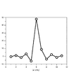
図3は、第2の遅延回路131による光信号の遅延例である。同図の縦軸は光信号の強度を示しており、L0が4値の光信号の最低レベルを表し、L3が4値の光信号の最高レベルを表している。また、同図の横軸は時間を表している。第2の遅延回路131は、入力された第2のデジタル信号を、第2のデジタル信号の振幅レベルに線形に依存する遅延量だけ遅延させる。同図では、4値の光信号のピーク位置のずれを破線で示している。
FIG. 3 is an example of delaying an optical signal by the
同図に示す例では、波形の遅延量を−10%〜+10%としている。同図に示す例では、光信号の強度がL0からL3へ大きくなるに従って、遅延量が線形に大きくなるように遅延量を設定している。なお、波形の形状は光検出回路122等の特性によって変化する場合があり、その場合には遅延量を適宜変更することとしてよい。
In the example shown in the figure, the delay amount of the waveform is set to -10% to +10%. In the example shown in the figure, the delay amount is set so that the delay amount linearly increases as the optical signal intensity increases from L0 to L3. Note that the waveform shape may change depending on the characteristics of the
図4は、第2の遅延回路131による遅延がされない場合の光信号の受信例である。また、図5は、本発明の実施形態に係る光受信器120による光信号の受信例である。図4及び図5では、消光比が10.8dBである光信号のアイパターンを左側に示し、右側に波形中心時刻におけるヒストグラムを示している。図4に示すように、第2の遅延回路131による遅延がされない場合、アイパターンに大きな波形歪が生じ、波形中心時刻のヒストグラムにおいても4つの光信号レベルの分離が曖昧となっている。これに対して、図5に示すように、本発明の実施形態に係る光受信器120により受信された光信号のアイパターンは、上下3つのアイ開口のタイミングがほぼ揃い、開口度がほぼ均等であり、波形中心時刻のヒストグラムにおいても4つの光信号レベルが良好に分離できている。
FIG. 4 is an example of receiving an optical signal when the
図6は、本発明の実施形態に係る第2の遅延回路131の機能ブロック図である。第2の遅延回路131は、量子化回路132と、第2の応答波形出力部133と、第2の遅延加算回路136と、を有する。第2の応答波形出力部133は、入力される第2のデジタル信号の振幅レベルに応じた波形で応答波形を出力する。第2の遅延加算回路136は、第2の応答波形出力部133から連続して出力された複数の第2の応答波形を、逐次遅延加算する。
FIG. 6 is a functional block diagram of the
量子化回路132は、第2の多値デジタル信号Xn(n:サンプル番号)の振幅レベルをN値(本例では−N/2〜N/2−1のN個の整数値)に量子化し、信号X’nを出力する。信号X’nは、第2の応答波形出力部133に入力される。第2の応答波形出力部133は、応答波形ルックアップテーブル134を有する。応答波形ルックアップテーブル134には、それぞれ長さMサンプルであるN個の応答波形(y(i,j)、i=1〜N、j=1〜M)が記憶されており、第2の応答波形出力部133は、信号X’nの値に応じて長さMサンプルの第2の応答波形y(X’n,j)(j=1〜M)を出力する。第2の応答波形は、第2の遅延加算回路136に入力され、その内部に記憶された過去Mサンプル分の逐次加算波形u(j)(j=1〜M)に逐次加算される。逐次加算波形u(j)は順次右シフトされ、右端成分が出力信号Znとして出力される。すなわち、第2の遅延加算回路136は、j=1についてu(1)=0、j=1〜M−1についてu(j+1)=u(j)+y(X’n,j)、j=MについてZn=u(M)+y(X’n,M)と演算する。
The
なお、量子化回路132による量子化レベルNは、小さい値とすることで応答波形ルックアップテーブル134のインデックス数を削減し、記憶容量や回路規模を縮小することができるが、その一方で波形補正精度が十分に高められないおそれがあるため、量子化レベルNの値は両者のトレードオフによって適切な値に設計されるべきものである。量子化回路132は、第2の多値デジタル信号の振幅情報の下位ビットの切り捨てによっても実現可能であり、量子化回路132を省略することも可能である。
By setting the quantization level N by the
第2の遅延回路131により、入力された第2のデジタル信号Xnを、第2のデジタル信号Xnの振幅レベルに線形に依存する遅延量だけ遅延させる場合、応答波形ルックアップテーブル134には、y(i)=IDFT[i×exp(−√−1×2π(iT))]をM個に時間サンプリングした波形を収容すればよい。ここで、IDFTは離散逆フーリエ変換を表し、√−1は虚数単位である。このようにして得られる波形の遅延量は、最大振幅値でNT/2−1、最小振幅値で−NT/2となる。
When the
図7は、応答波形ルックアップテーブル134に収容される応答波形の第1の例である。図8は、応答波形ルックアップテーブル134に収容される応答波形の第2の例である。図9は、応答波形ルックアップテーブル134に収容される応答波形の第3の例である。図7〜9に示す応答波形の例は、長さが11サンプル(j=1〜11)であり、量子化レベルNは128(i=−64〜63)である。図7では、振幅レベルが大きい場合(i=49)に出力される応答波形の例を示し、図8では、振幅レベルがやや大きい場合(i=39)に出力される応答波形の例を示し、図9では、振幅レベルが中間程度である場合(i=1)に出力される応答波形の例を示している。図示しないが、振幅レベルが小さい場合(i=−49)に出力される応答波形は、図7に示す波形をj=6を中心に反転したものであり、振幅レベルがやや小さい場合(i=−39)に出力される応答波形は、図8に示す波形をj=6を中心に反転したものである。 FIG. 7 is a first example of response waveforms stored in the response waveform lookup table 134. FIG. 8 is a second example of response waveforms stored in the response waveform lookup table 134. FIG. 9 is a third example of the response waveform stored in the response waveform lookup table 134. In the response waveform examples shown in FIGS. 7 to 9, the length is 11 samples (j=1 to 11), and the quantization level N is 128 (i=−64 to 63). FIG. 7 shows an example of the response waveform output when the amplitude level is large (i=49), and FIG. 8 shows an example of the response waveform output when the amplitude level is slightly large (i=39). , FIG. 9 shows an example of the response waveform output when the amplitude level is about the middle level (i=1). Although not shown, the response waveform output when the amplitude level is small (i=-49) is the waveform shown in FIG. 7 inverted around j=6, and when the amplitude level is slightly small (i= The response waveform output at −39) is the waveform shown in FIG. 8 inverted with j=6 as the center.
図9に示すように、振幅レベルが中間程度である場合(i=1)に出力される応答波形は、高さ1のインパルス応答波形に近いものであり、遅延量がほぼ0である。一方、図7及び8に示すように、振幅レベルが大きい場合(i=49)に出力される応答波形と、振幅レベルがやや大きい場合(i=39)に出力される応答波形は、振幅レベルに比例した遅延量となるよう歪みを加えられたインパルス応答波形となっている。
As shown in FIG. 9, when the amplitude level is about the middle level (i=1), the response waveform output is close to the impulse response waveform of
なお本実施形態では、第2の多値デジタル信号Xnの振幅レベルを、0を中心値として−N/2〜N/2−1の値域にあるものとしたが、中心値及び値域は任意の値として構わない。遅延量についても、振幅レベルが0のときにほぼ0となるように選んだが、任意の固定値を遅延量に加えてもよい。また、応答波形ルックアップテーブル134に収容される応答波形は、デルタ関数とその遅延に限るものではなく、任意の形状の応答関数とその遅延を利用することが可能である。例えば、光送受信器10の部品の応答関数の逆関数を利用することによって、周波数特性の補正効果を併せもたせることもできる。
In the present embodiment, the amplitude level of the second multilevel digital signal Xn is in the range of −N/2 to N/2-1 with 0 as the center value, but the center value and the range of values are arbitrary. It doesn't matter as a value. The delay amount is also selected to be almost 0 when the amplitude level is 0, but an arbitrary fixed value may be added to the delay amount. Further, the response waveform stored in the response waveform lookup table 134 is not limited to the delta function and its delay, but a response function of any shape and its delay can be used. For example, by utilizing the inverse function of the response function of the component of the optical transmitter/
図10は、半導体レーザの緩和振動周波数に基づき決定された遅延量の例である。同図の縦軸は遅延量を示し、横軸は半導体レーザの変調電流値Iを示す。第2の遅延回路131により、入力された第2のデジタル信号Xnを、第2のデジタル信号Xnの振幅レベルに非線形に依存する遅延量だけ遅延させる場合、同図に示す遅延量を採用することができる。この場合、第2の遅延回路131は、入力された第2のデジタル信号Xnを、第2のデジタル信号Xnの振幅レベルに応じて、半導体レーザの緩和振動周波数の逆数に比例する遅延量だけ遅延させる。
FIG. 10 is an example of the delay amount determined based on the relaxation oscillation frequency of the semiconductor laser. The vertical axis of the figure shows the delay amount, and the horizontal axis shows the modulation current value I of the semiconductor laser. When the
半導体レーザを直接変調する場合の応答速度は、レーザの変調電流値Iに依存して非線形に変化する。半導体レーザの応答遅延Tは、半導体レーザの緩和振動周波数Frの逆数を用いて、T=1/Fr=C/√(I/Ith−1)と近似的に表される。ここで、Cは遅延定数であり、Iはレーザ変調電流であり、Ithはレーザ閾値電流である。第2の遅延回路131により、入力された第2のデジタル信号Xnを、第2のデジタル信号Xnの振幅レベルに応じて、半導体レーザの緩和振動周波数の逆数に比例する遅延量だけ遅延させる場合、応答波形ルックアップテーブル134には、図10に示す遅延量のインパルス応答関数を収容すればよい。すなわち、バイアス電流Ib=40mA、変調電流の振幅が±25mAの場合、最低振幅レベルL0では遅延量を0とし、最高振幅レベルL3では遅延量を−1.0程度とする。
The response speed in the case of directly modulating the semiconductor laser changes non-linearly depending on the modulation current value I of the laser. The response delay T of the semiconductor laser is approximately expressed as T=1/Fr=C/√(I/Ith−1) using the reciprocal of the relaxation oscillation frequency Fr of the semiconductor laser. Here, C is a delay constant, I is a laser modulation current, and Ith is a laser threshold current. When the
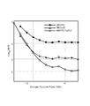
図11は、光信号のビット誤り率と平均受信強度の関係を示す図である。同図の縦軸には、ビット誤り率の対数値を示し、横軸には受光した光信号の平均受信強度を示している。消光劣化により送信波形が劣化した場合、平均受信強度を増大してもビット誤り率が一定値以下に下がらないエラーフロアという現象が生じることが知られている。エラーフロアの誤り率が高く、受信器内の誤り訂正回路の訂正閾値を上回ると、誤り訂正が不可能となり、信号伝送ができなくなる。このような誤り訂正回路の訂正閾値としては、例えば高速伝送の次世代規格の代表であるIEEEの400ギガイーサ標準規格では2×10⁻⁴とされている。 FIG. 11 is a diagram showing the relationship between the bit error rate of an optical signal and the average reception intensity. The vertical axis of the figure shows the logarithmic value of the bit error rate, and the horizontal axis shows the average reception intensity of the received optical signal. It is known that when the transmission waveform is deteriorated due to extinction deterioration, an error floor occurs in which the bit error rate does not drop below a certain value even if the average reception intensity is increased. If the error rate of the error floor is high and exceeds the correction threshold of the error correction circuit in the receiver, error correction becomes impossible and signal transmission becomes impossible. The correction threshold of such an error correction circuit is, for example, 2×10 −4 in the IEEE 400 gigaisa standard, which is a representative of the next-generation standard for high-speed transmission.
同図では、黒塗り四角のプロット点により、特に補正を行わない場合(第2の遅延回路131による遅延がされない場合)の光信号のビット誤り率と平均受信強度の関係を示している。第2の遅延回路131による遅延がされない場合、平均受信強度が−3〜−8dBmである場合、ビット誤り率は10−3程度であり、平均受信強度が−9〜−12dBmと大きくなるに従って、ビット誤り率は8×10⁻³程度に悪化している。
In the same figure, the plot points of the black squares show the relationship between the bit error rate of the optical signal and the average reception intensity when no particular correction is made (when the
図11では、比較例として、Volterra非線形適応等化器により受信波形を補正した場合の例を、白抜き三角のプロット点で示している。比較例では、平均受信強度が−3〜−10dBmである場合、ビット誤り率が4×10⁻³〜10−4程度に改善している。 In FIG. 11, as a comparative example, an example in which the received waveform is corrected by the Volterra nonlinear adaptive equalizer is shown by white triangle plot points. In the comparative example, when the average reception intensity is -3 to -10 dBm, the bit error rate is improved to about 4×10 -3 to 10 -4 .
図11では、本実施形態に係る光受信器120により受信された光信号のビット誤り率と平均受信強度の関係を、第2のデジタル信号の振幅レベルに線形に依存する遅延量だけ遅延させた場合のうち遅延量が10%である例を十字のプロット点で示し、遅延量が17.5%である例をクロスマークのプロット点により示している。また、第2のデジタル信号の振幅レベルに非線形に依存する遅延量だけ遅延させ、第2のデジタル信号の振幅レベルに応じて、半導体レーザの緩和振動周波数の逆数に比例する遅延量だけ遅延させた例を白抜き丸のプロット点で示している。
In FIG. 11, the relationship between the bit error rate and the average reception intensity of the optical signal received by the
第2のデジタル信号の振幅レベルに線形に依存する遅延量を10%として遅延させた場合(図中の十字のプロット点の場合)、平均受信強度が−3〜−10dBmのときに、ビット誤り率が8×10⁻⁴〜3×10⁻⁴程度に改善している。また、第2のデジタル信号の振幅レベルに線形に依存する遅延量を17.5%として遅延させた場合(図中のクロスマークのプロット点の場合)、平均受信強度が−3〜−10dBmのときに、ビット誤り率が3×10⁻⁴〜9×10⁻⁵程度に改善している。同図に示されているように、本実施形態に係る光受信器120によれば、第2の遅延回路131による遅延がされることで、第2の遅延回路131による遅延がされない場合と比較して、ビット誤り率が1桁程度改善する。また、第2のデジタル信号の振幅レベルに線形に依存する遅延量を適切に選択することで、大規模な補正回路を要するVolterra非線形適応等化器を用いた場合よりも良好なビット誤り率を得ることができる。またエラーフロアもおよそ9×10⁻⁵となり、前述の誤り訂正閾値を下回り正常な情報伝送が実現できる。
When the delay amount that linearly depends on the amplitude level of the second digital signal is set to 10% and delayed (in the case of a cross plot point in the figure), a bit error occurs when the average reception intensity is -3 to -10 dBm. The rate is improved to about 8×10 −4 to 3×10 −4 . When the delay amount that linearly depends on the amplitude level of the second digital signal is set to 17.5% (in the case of the plot point of the cross mark in the figure), the average reception intensity is -3 to -10 dBm. At times, the bit error rate is improved to about 3×10 −4 to 9×10 −5 . As shown in the figure, according to the
第2のデジタル信号の振幅レベルに応じて、半導体レーザの緩和振動周波数の逆数に比例する遅延量だけ遅延させた場合、平均受信強度が−3〜−10dBmのときに、ビット誤り率が10−4〜2×10⁻⁵程度に改善している。本実施形態に係る光受信器120によれば、第2の遅延回路131によって半導体レーザの緩和振動周波数の逆数に比例する遅延量だけ遅延がされることで、第2の遅延回路131による遅延がされない場合と比較して、ビット誤り率が2桁以上改善する。また、大規模な補正回路を要するVolterra非線形適応等化器を用いた場合と比較しても、ビット誤り率が1/4程度にまで改善する。
When delayed by a delay amount proportional to the reciprocal of the relaxation oscillation frequency of the semiconductor laser according to the amplitude level of the second digital signal, the bit error rate is 10 − when the average reception intensity is −3 to −10 dBm. It is improved to about 4 to 2×10 −5 . According to the
本実施形態に係る第2の遅延回路131は、半導体レーザの直接変調に起因する非線形な波形歪のうち位相方向の遅延のみをデジタル的に補正するものであり、Volterra非線形適応等化器等の従来例と比較して、収束性や安定性の問題が生じないより簡素で安価な回路構成で、より演算負荷が軽く、高精度な波形補正を行うことができる。
The
なお、本実施形態では、光強度多値信号としてPAM(Pulse−Amplitude Modulation)4信号の場合を示したが、多値変調の種類や符号化方法は異なってもよい。例えば、8値(PAM8)や16値(PAM16)などの高次のPAM信号や、前後の多値シンボルとの符号間干渉を許容したパーシャルレスポンス型の強度多値信号、トレリス符号化を組み合わせた高次の光強度多値信号等を採用してもよい。本実施形態に係る第2の遅延回路131は、光信号の振幅レベルに応じた波形遅延を行うものであり、多値信号の種類を問わず適用可能だからである。また、多値信号の一種として、帯域の狭いナイキストフィルタを用いて、多値信号の狭帯域化を図るナイキスト多値変調を採用してもよい。ナイキスト多値変調は、シンボル境界付近で多値信号の上下に大きな振幅のピーキングをもつという特徴があるが、波形のピーキングを含めて実際の変調電流に対応した波形遅延が加えられるようにすれば、他の多値信号と同様に本実施形態に係る第2の遅延回路131によって扱うことができる。ナイキスト多値変調と同様のピーキングをもつサブキャリア変調や、その一種であるDMT(Discrete Multi Tone)変調などについても同様である。
In the present embodiment, the case of four PAM (Pulse-Amplitude Modulation) signals as the light intensity multilevel signal is shown, but the type of multilevel modulation and the encoding method may be different. For example, a high-order PAM signal such as 8-value (PAM8) or 16-value (PAM16), a partial response-type intensity multi-value signal that allows intersymbol interference with preceding and following multi-value symbols, and trellis coding are combined. Higher-order light intensity multilevel signals or the like may be adopted. This is because the
図12は、本発明の実施形態の変形例に係る第2の遅延回路131の機能ブロック図である。変形例に係る第2の遅延回路131は、図6に示す第2の遅延回路131と比較して、アップサンプリング回路140と、振幅セレクタ回路141と、個別遅延回路142と、加算回路143と、ダウンダンプリング回路144と、を有する点で異なる。変形例に係る第2の遅延回路131は、図6に示す第2の遅延回路131と比較して、量子化回路132を有する点で同様の構成を有する。
FIG. 12 is a functional block diagram of the
量子化回路132は、第2の多値デジタル信号Xn(n:サンプル番号)の振幅レベルをN値(本例では−N/2〜N/2−1のN個の整数値)に量子化し、信号X’nをアップサンプリング回路140に出力する。アップサンプリング回路140は、サンプル間に一定数のゼロ信号を挿入し、波形の時間分解能を高めて、信号X’’nを振幅セレクタ回路141に出力する。振幅セレクタ回路141は、N値の信号X’’nの振幅値(本例では0〜N−1)に応じて、入力信号X’’nを個別遅延回路142に出力する。個別遅延回路142は、入力信号の振幅レベルに応じた遅延量を与えて、加算回路143に出力する。加算回路143は、個別遅延回路142により遅延された信号を加算して、ダウンダンプリング回路144に信号Z’nを出力する。ダウンダンプリング回路144は、信号Z’nを元のサンプリング速度の波形に戻して、信号Znを出力する。
The
個別遅延回路142は、入力された信号を、信号の振幅レベルに線形に依存する遅延量だけ遅延させてもよいし、入力された信号を、信号の振幅レベルに非線形に依存する遅延量だけ遅延させてもよい。また、個別遅延回路142は、入力された信号を、信号の振幅レベルに応じて、半導体レーザの緩和振動周波数の逆数に比例する遅延量だけ遅延させてもよい。このような構成を採用する場合であっても、図11に示す良好な平均受信強度とビット誤り率の関係を得ることができる。
The
変形例に係る個別遅延回路142は、単純なデータ遅延のみを行う回路であり、シフトレジスタ等の簡易な回路で実装可能である利点がある。アップサンプリング回路140によって処理すべきデータ量は、量子化レベルNに応じて増大するものの、ほとんどはゼロ値であるため、非ゼロサンプル値についてのみ処理を行うことによって実質的な回路規模の増加はない。
The
図13は、本発明の実施形態の変形例に係る光受信器120の機能ブロック図である。変形例に係る光受信器120は、図2に示す光受信器120の構成に加えて、誤り率検出部128と、遅延量修正部129と、を有する。誤り率検出部128は、多値復号回路125から出力された第2の情報信号の誤り率を検出する。遅延量修正部129は、誤り率検出部128により検出された誤り率に基づいて、第2の遅延回路131の遅延量を修正する。誤り率検出部128は、受信側線形等化回路124から出力された第2の多値デジタル信号の波形誤差を検出してもよい。
FIG. 13 is a functional block diagram of an
遅延量修正部129は、誤り率検出部128で検出される誤り率が小さくなるように、第2の遅延回路131の遅延量を修正する。遅延量修正部129は、応答波形ルックアップテーブル134の応答波形を修正したり、個別遅延回路142の遅延量を修正したりすることで、第2の遅延回路131の遅延量を修正する。誤り率検出部128及び遅延量修正部129を有することで、常に最適の遅延量が設定され、誤り率が小さく保たれる。
The delay
図14は、本発明の実施形態に係る光送信器100の機能ブロック図である。光送信器100は、入力された第1の情報信号に応じて、第1の電気信号を出力する光送信集積回路101と、レーザ電流駆動回路105と、バイアス電流加算回路106と、バイアス電流源107と、光強度が変調された光信号を光ファイバ110に出力する半導体レーザ108と、備える。レーザ電流駆動回路105は、光送信集積回路101から出力される第1の電気信号に基づいて、変調電流を出力する。バイアス電流加算回路106は、バイアス電流源107から出力されるバイアス電流を変調電流に加算する。バイアス電流は、例えば40mAであり、変調電流は±25mAとしてよい。
FIG. 14 is a functional block diagram of the
光送信集積回路101は、入力された第1の情報信号に応じて、第1の多値デジタル信号を出力する多値符号化回路102と、入力された第1の多値デジタル信号を、第1の多値デジタル信号の振幅レベルに応じた遅延量だけ遅延させる第1の遅延回路130と、第1の遅延回路130により遅延された第1の多値デジタル信号を第1の電気信号に変換するDA(Digital to Analog)変換器104と、を有する。また、光送信集積回路101は、送信側線形等化回路103を有する。送信側線形等化回路103は、第1の遅延回路130により遅延された第1の多値デジタル信号について、高周波部品に起因する線形劣化を補正し、DA変換器104に出力する。
The optical transmission integrated
第1の遅延回路130の構成として、図6に示した第2の遅延回路131の構成をそのまま適用できる。すなわち、第1の遅延回路130は、入力される第1のデジタル信号の振幅レベルに応じた波形で応答波形を出力する第1の応答波形出力部(図6の第2の応答波形出力部133に相当)と、第1の応答波形出力部から連続して出力された複数の第1の応答波形を、逐次遅延加算する第1の遅延加算回路(図6の第2の遅延加算回路136に相当)と、を有してよい。また、第1の遅延回路130の他の構成として、図12に示した変形例に係る第2の遅延回路131の構成をそのまま適用することとしてもよい。
As the configuration of the
第1の遅延回路130において、入力信号Xnは第1の多値デジタル信号であり、出力信号Znは送信側線形等化回路103に入力される。第1の遅延回路130は、入力された第1のデジタル信号を、第1のデジタル信号の振幅レベルに線形に依存する遅延量だけ遅延させることとしてよい。また、第1の遅延回路130は、入力された第1のデジタル信号を、第1のデジタル信号の振幅レベルに非線形に依存する遅延量だけ遅延させてもよく、入力された第1のデジタル信号を、第1のデジタル信号の振幅レベルに応じて、半導体レーザ108の緩和振動周波数の逆数に比例する遅延量だけ遅延させてもよい。
In the
本実施形態に係る光送信集積回路101は、第1の遅延回路130を有することで、第2の遅延回路131を有する光受信集積回路121と比較して、入力信号Xnのレベル数が大きく削減されるため、回路規模を小さくすることができる。PAM4信号のレベル数は、1サンプル/シンボルの信号処理の場合には4であり、2サンプル/シンボルの場合には7であるため、応答波形ルックアップテーブル134のメモリ数を4又は7に削減することができる(入力信号の振幅レベルをN=4又は7にできる)。これにより、光送信集積回路101に含まれる応答波形ルックアップテーブル134の回路規模は、光受信集積回路121の場合と比較して1/10〜1/100となり、回路規模と消費電力を低減することができる。また、光送信集積回路101では、第1の遅延回路130が半導体レーザ108に近接して配置されるため、個々のレーザの特性や消光比などの特性に合わせて、第1の遅延回路130についてより正確な遅延特性を設定することも可能となり、補正精度の向上により、損失耐力の向上や伝送距離の延長が行える。
The optical transmission integrated
図15は、光信号のビット誤り率と平均受信強度の関係を示す図である。同図の縦軸には、ビット誤り率の対数値を示し、横軸には光信号の平均受信強度を示している。同図では、黒塗り四角のプロット点により、特に補正を行わない場合(第1の遅延回路130による遅延がされない場合)の光信号のビット誤り率と平均受信強度の関係を示している。第1の遅延回路130による遅延がされない場合、平均受信強度が−3〜−8dBmである場合、ビット誤り率は1×10⁻³〜3×10⁻³程度に悪化している。
FIG. 15 is a diagram showing the relationship between the bit error rate of an optical signal and the average reception intensity. The vertical axis of the figure shows the logarithmic value of the bit error rate, and the horizontal axis shows the average reception intensity of the optical signal. In the same figure, the black square plot points show the relationship between the bit error rate of the optical signal and the average reception intensity when no particular correction is performed (when the
図15では、比較例として、Volterra非線形適応等化器により光受信器側で受信波形を補正した場合の例を、白抜き三角のプロット点で示している。比較例では、平均受信強度が−3〜−10dBmである場合、ビット誤り率が4×10⁻³〜10−4程度に改善している。 In FIG. 15, as a comparative example, an example in which the received waveform is corrected on the optical receiver side by the Volterra non-linear adaptive equalizer is shown by white triangle plot points. In the comparative example, when the average reception intensity is -3 to -10 dBm, the bit error rate is improved to about 4×10 -3 to 10 -4 .
図15では、本実施形態に係る光送信器100により送信された光信号のビット誤り率と平均受信強度の関係を、第2のデジタル信号の振幅レベルに非線形に依存する遅延量だけ遅延させ、第2のデジタル信号の振幅レベルに応じて、半導体レーザ108の緩和振動周波数の逆数に比例する遅延量だけ遅延させた例を白抜きの丸のプロット点で示している。
In FIG. 15, the relationship between the bit error rate of the optical signal transmitted by the
第1のデジタル信号の振幅レベルに応じて、半導体レーザ108の緩和振動周波数の逆数に比例する遅延量だけ遅延させた場合(図中の白抜きの丸のプロット点の場合)、平均受信強度が−3〜−10dBmのときに、ビット誤り率が4×10⁻⁴〜10−5程度に改善している。本実施形態に係る光受信器120によれば、第1の遅延回路130によって半導体レーザ108の緩和振動周波数の逆数に比例する遅延量だけ遅延がされることで、第1の遅延回路130による遅延がされない場合と比較して、ビット誤り率が2桁以上改善する。また、大規模な補正回路を要するVolterra非線形適応等化器を用いた場合と比較しても、ビット誤り率が1/4程度に改善する。また、第1のデジタル信号の振幅レベルに応じて、半導体レーザ108の緩和振動周波数の逆数に比例する遅延量だけ遅延させた場合のエラーフロアは、1×10−5程度であり、前述の誤り訂正閾値を十分下回り、正常な情報伝送が実現できる。
When the delay amount is delayed in proportion to the reciprocal of the relaxation oscillation frequency of the
本実施形態に係る第1の遅延回路130は、半導体レーザ108の直接変調に起因する非線形な波形歪のうち位相方向の遅延のみをデジタル的に補正するものであり、Volterra非線形適応等化器等の従来例と比較して、収束性や安定性の問題が生じないより簡素で安価な回路構成で、より演算負荷が軽く、高精度な波形補正を行うことができる。また、本実施形態に係る第1の遅延回路130は、光送信器100に設けられるものであり、Volterra非線形適応等化器のように光受信器のみに適用可能なものではない。
The
図16は、本発明の実施形態の変形例に係る光送信器100の機能ブロック図である。変形例に係る光送信器100は、図14に示す光送信器100の構成に加えて、半導体レーザ108の変調条件を設定する変調条件設定部112と、変調条件に基づいて、第1の遅延回路130の遅延量を修正する遅延量修正部113と、をさらに有する。
FIG. 16 is a functional block diagram of an
半導体レーザ108の変調条件を変更すると、光信号の波形が変化するため、遅延量修正部113は、半導体レーザ108の変調条件に基づいて、常に精密な波形補正を行うように調整する。半導体レーザ108の変調条件は、バイアス電流値と、変調振幅により定められ、遅延量修正部113は、これらに加えて半導体レーザ108の閾値電流や消光比等のパラメータを利用してもよい。また、半導体レーザ108の温度による緩和振動周波数の変化を考慮して、半導体レーザ108のチップ温度に基づいて、第1の遅延回路130の遅延量を修正してもよい。
When the modulation condition of the
図17は、本発明の実施形態の変形例に係る第1の遅延回路130の機能ブロック図である。変形例に係る第1の遅延回路130は、量子化回路132と、アップサンプリング回路140と、振幅セレクタ回路141と、個別遅延回路142と、加算回路143と、ダウンダンプリング回路144と、を有し、個別遅延回路142に遅延量修正部113からの信号が入力される。
FIG. 17 is a functional block diagram of the
量子化回路132は、第1の多値デジタル信号Xn(n:サンプル番号)の振幅レベルをN値(本例では−N/2〜N/2−1のN個の整数値)に量子化し、信号X’nをアップサンプリング回路140に出力する。アップサンプリング回路140は、サンプル間に一定数のゼロ信号を挿入し、波形の時間分解能を高めて、信号X’’nを振幅セレクタ回路141に出力する。振幅セレクタ回路141は、N値の信号X’’nの振幅値(本例では0〜N−1)に応じて、入力信号X’’nを個別遅延回路142に出力する。個別遅延回路142は、入力信号の振幅レベルに応じた遅延量を与えて、加算回路143に出力する。加算回路143は、個別遅延回路142により遅延された信号を加算して、ダウンダンプリング回路144に信号Z’nを出力する。ダウンダンプリング回路144は、信号Z’nを元のサンプリング速度の波形に戻して、信号Znを出力する。
The
個別遅延回路142は、入力された信号を、信号の振幅レベルに線形に依存する遅延量だけ遅延させてもよいし、入力された信号を、信号の振幅レベルに非線形に依存する遅延量だけ遅延させてもよい。また、個別遅延回路142は、入力された信号を、信号の振幅レベルに応じて、半導体レーザの緩和振動周波数の逆数に比例する遅延量だけ遅延させてもよい。また、個別遅延回路142は、遅延量修正部113から入力される信号に基づいて、遅延量を修正する。
The
変形例の個別遅延回路142は、単純なデータ遅延のみを行う回路であり、シフトレジスタ等の簡易な回路で実装可能である利点がある。アップサンプリング回路140によって処理すべきデータ量は量子化レベルNに応じて増大するものの、ほとんどはゼロ値であるため、非ゼロサンプル値についてのみ処理を行うことによって実質的な回路規模の増加はない。また、遅延量修正部113によって常に遅延量が最適に保たれ、光信号の誤り率が小さく保たれる。
The
以上、本発明に係る実施形態について説明したが、この実施形態に示した具体的な構成は一例として示したものであり、本発明の技術的範囲をこれに限定することは意図されていない。例えば、本実施形態では、強度変調された光信号を電気信号に変換する光検出回路122を例示した。光検出回路122としては、他の方式のものを採用することも可能であり、例えば、半導体や希土類添加光ファイバ型の光増幅器を光検出回路122の前に配置した前置光増幅型光受信機、APD(Avalanche PhotoDiode)を用いた光増倍型光受信器、光遅延干渉を用いた光遅延検波型受信器、受信器内部に局発レーザを配置するコヒーレント光受信器等を採用することもできる。
Although the embodiment of the present invention has been described above, the specific configuration shown in this embodiment is shown as an example, and the technical scope of the present invention is not intended to be limited thereto. For example, the present embodiment exemplifies the
10 光送受信器、100 光送信器、101 光送信集積回路、102 多値符号化回路、103 送信側線形等化回路、104 DA変換器、105 レーザ電流駆動回路、106 バイアス電流加算回路、107 バイアス電流源、108 半導体レーザ、110 光ファイバ、112 変調条件設定部、113 遅延量修正部、120 光受信器、121 光受信集積回路、122 光検出回路、123 AD変換器、124 受信側線形等化回路、125 多値復号回路、128 誤り率検出部、129 遅延量修正部、130 第1の遅延回路、131 第2の遅延回路、132 量子化回路、133 第2の応答波形出力部、134 応答波形ルックアップテーブル、135 第2の応答波形、136 第2の遅延加算回路、140 アップサンプリング回路、141 振幅セレクタ回路、142 個別遅延回路、143 加算回路、144 ダウンサンプリング回路。 10 optical transceiver, 100 optical transmitter, 101 optical transmission integrated circuit, 102 multi-level encoding circuit, 103 transmission side linear equalization circuit, 104 DA converter, 105 laser current drive circuit, 106 bias current addition circuit, 107 bias Current source, 108 semiconductor laser, 110 optical fiber, 112 modulation condition setting unit, 113 delay amount correcting unit, 120 optical receiver, 121 optical receiving integrated circuit, 122 photodetecting circuit, 123 AD converter, 124 receiving side linear equalization Circuit, 125 multi-level decoding circuit, 128 error rate detection unit, 129 delay amount correction unit, 130 first delay circuit, 131 second delay circuit, 132 quantization circuit, 133 second response waveform output unit, 134 response Waveform lookup table, 135 Second response waveform, 136 Second delay addition circuit, 140 Upsampling circuit, 141 Amplitude selector circuit, 142 Individual delay circuit, 143 Addition circuit, 144 Downsampling circuit.
Claims (10)
入力された前記第1の多値デジタル信号を、前記第1の多値デジタル信号の振幅レベルに応じた遅延量だけ遅延させる第1の遅延回路と、
前記第1の遅延回路により遅延された前記第1の多値デジタル信号を第1の電気信号に変換するDA変換器と、
前記第1の電気信号に応じて、光強度が変調された光信号を出力する半導体レーザと、を有する光送信器と、
前記光信号を受光して第2の電気信号を出力する光検出回路と、
前記第2の電気信号を第2の多値デジタル信号に変換するAD変換器と、
前記第2の多値デジタル信号を復号して、第2の情報信号を出力する多値復号回路と、を有する光受信器と、
を備える光送受信器。 A multi-level encoding circuit that outputs a first multi-level digital signal in response to the input first information signal;
A first delay circuit for delaying the input first multi-level digital signal by a delay amount according to the amplitude level of the first multi-level digital signal;
A DA converter for converting the first multilevel digital signal delayed by the first delay circuit into a first electric signal;
An optical transmitter having a semiconductor laser that outputs an optical signal whose optical intensity is modulated according to the first electric signal;
A photodetector circuit for receiving the optical signal and outputting a second electric signal;
An AD converter for converting the second electric signal into a second multilevel digital signal;
An optical receiver having a multilevel decoding circuit for decoding the second multilevel digital signal and outputting a second information signal;
Optical transmitter/ receiver.
前記光受信器は、前記第2の多値デジタル信号を、前記第2の多値デジタル信号の振幅レベルに応じた遅延量だけ遅延させる第2の遅延回路を有し、
前記多値復号回路は、前記第2の遅延回路により遅延された前記第2の多値デジタル信号を復号して、前記第2の情報信号を出力する、
光送受信器。 The optical transceiver according to claim 1, wherein:
The optical receiver includes a second delay circuit that delays the second multilevel digital signal by a delay amount according to an amplitude level of the second multilevel digital signal ,
The multi-level decoding circuit decodes the second multi-level digital signal delayed by the second delay circuit and outputs the second information signal,
Optical transceiver.
前記光受信器は、
前記多値復号回路から出力された前記第2の情報信号の誤り率を検出する誤り率検出部と、
前記誤り率に基づいて、前記第2の遅延回路の遅延量を修正する遅延量修正部と、をさらに有する、
光送受信器。 The optical transceiver according to claim 2, wherein
The optical receiver is
An error rate detection unit that detects an error rate of the second information signal output from the multilevel decoding circuit;
A delay amount correction unit that corrects the delay amount of the second delay circuit based on the error rate.
Optical transceiver.
前記光送信器は、
前記半導体レーザの変調条件を設定する変調条件設定部と、
前記変調条件に基づいて、前記第1の遅延回路の遅延量を修正する遅延量修正部と、をさらに有する、
光送受信器。 The optical transceiver according to claim 1 , wherein:
The optical transmitter is
A modulation condition setting unit for setting the modulation condition of the semiconductor laser;
A delay amount correction unit that corrects the delay amount of the first delay circuit based on the modulation condition,
Optical transceiver.
前記第1の遅延回路は、入力された前記第1の多値デジタル信号を、前記第1の多値デジタル信号の振幅レベルに線形に依存する遅延量だけ遅延させ、
前記第2の遅延回路は、入力された前記第2の多値デジタル信号を、前記第2の多値デジタル信号の振幅レベルに線形に依存する遅延量だけ遅延させる、
光送受信器。 The optical transceiver according to claim 2 , wherein
The first delay circuit delays the input first multilevel digital signal by a delay amount that linearly depends on an amplitude level of the first multilevel digital signal,
The second delay circuit delays the input second multilevel digital signal by a delay amount that linearly depends on the amplitude level of the second multilevel digital signal.
Optical transceiver.
前記第1の遅延回路は、入力された前記第1の多値デジタル信号を、前記第1の多値デジタル信号の振幅レベルに非線形に依存する遅延量だけ遅延させ、
前記第2の遅延回路は、入力された前記第2の多値デジタル信号を、前記第2の多値デジタル信号の振幅レベルに非線形に依存する遅延量だけ遅延させる、
光送受信器。 The optical transceiver according to claim 2 , wherein
The first delay circuit delays the input first multi-level digital signal by a delay amount that is non-linearly dependent on the amplitude level of the first multi-level digital signal,
The second delay circuit delays the input second multilevel digital signal by a delay amount that is non-linearly dependent on the amplitude level of the second multilevel digital signal.
Optical transceiver.
前記第1の遅延回路は、入力された前記第1の多値デジタル信号を、前記第1の多値デジタル信号の振幅レベルに応じて、前記半導体レーザの緩和振動周波数の逆数に比例する遅延量だけ遅延させ、
前記第2の遅延回路は、入力された前記第2の多値デジタル信号を、前記第2の多値デジタル信号の振幅レベルに応じて、前記半導体レーザの緩和振動周波数の逆数に比例する遅延量だけ遅延させる、
光送受信器。 The optical transceiver according to claim 6 , wherein
The first delay circuit, based on the amplitude level of the first multilevel digital signal, delays the input first multilevel digital signal in proportion to the reciprocal of the relaxation oscillation frequency of the semiconductor laser. Delay only
The second delay circuit delays the input second multilevel digital signal in proportion to the reciprocal of the relaxation oscillation frequency of the semiconductor laser in accordance with the amplitude level of the second multilevel digital signal. Only delay,
Optical transceiver.
前記第1の多値デジタル信号を第1の電気信号に変換するDA変換器と、
前記第1の電気信号に応じて、光強度が変調された光信号を出力する半導体レーザと、を有する光送信器と、
前記光信号を受光して第2の電気信号を出力する光検出回路と、
前記第2の電気信号を第2の多値デジタル信号に変換するAD変換器と、
前記第2の多値デジタル信号を復号して、第2の情報信号を出力する多値復号回路と、を有する光受信器と、
を備える光送受信器であって、
前記光送信器に含まれ、入力された前記第1の多値デジタル信号を、前記第1の多値デジタル信号の振幅レベルに応じた遅延量だけ遅延させる回路であり、
入力される前記第1の多値デジタル信号の振幅レベルに応じた波形で応答波形を出力する第1の応答波形出力部と、
前記第1の応答波形出力部から連続して出力された複数の第1の応答波形を、逐次遅延加算する第1の遅延加算回路と、を有した第1の遅延回路、及び、
前記光受信器に含まれ、入力された前記第2の多値デジタル信号を、前記第2の多値デジタル信号の振幅レベルに応じた遅延量だけ遅延させる回路であり、
入力される前記第2の多値デジタル信号の振幅レベルに応じた波形で応答波形を出力する第2の応答波形出力部と、
前記第2の応答波形出力部から連続して出力された複数の第2の応答波形を、逐次遅延加算する第2の遅延加算回路と、を有した第2の遅延回路、
の少なくともいずれか一方をさらに備えた、
光送受信器。 A multi-level encoding circuit that outputs a first multi-level digital signal in response to the input first information signal;
A DA converter for converting the first multi-valued digital signal into a first electric signal;
An optical transmitter having a semiconductor laser that outputs an optical signal whose optical intensity is modulated according to the first electric signal;
A photodetector circuit for receiving the optical signal and outputting a second electric signal;
An AD converter for converting the second electric signal into a second multilevel digital signal;
An optical receiver having a multilevel decoding circuit for decoding the second multilevel digital signal and outputting a second information signal;
An optical transceiver comprising:
A circuit which is included in the optical transmitter and delays the input first multilevel digital signal by a delay amount according to an amplitude level of the first multilevel digital signal,
A first response waveform output section for outputting a response waveform having a waveform corresponding to the amplitude level of the input first multilevel digital signal;
A first delay circuit including a first delay addition circuit for sequentially delay-adding a plurality of first response waveforms continuously output from the first response waveform output unit ; and
A circuit which is included in the optical receiver and delays the input second multilevel digital signal by a delay amount according to an amplitude level of the second multilevel digital signal,
A second response waveform output section for outputting a response waveform having a waveform corresponding to the amplitude level of the second multi-valued digital signal inputted;
Said second plurality of second response waveform output continuously from the response waveform output section of the second delay circuit possess a second delay addition circuit for sequentially delay addition, the,
Further comprising at least one of
Optical transceiver.
入力された前記第1の多値デジタル信号を、前記第1の多値デジタル信号の振幅レベルに応じた遅延量だけ遅延させる第1の遅延回路と、
前記第1の遅延回路により遅延された前記第1の多値デジタル信号を第1の電気信号に変換し、前記第1の電気信号に応じて、光強度が変調された光信号を出力する半導体レーザに前記第1の電気信号を出力するDA変換器と、
を有する光送信集積回路。 A multi-level encoding circuit that outputs a first multi-level digital signal in response to the input first information signal;
A first delay circuit for delaying the input first multi-level digital signal by a delay amount according to the amplitude level of the first multi-level digital signal;
A semiconductor that converts the first multi-level digital signal delayed by the first delay circuit into a first electric signal and outputs an optical signal whose light intensity is modulated according to the first electric signal. A DA converter for outputting the first electric signal to a laser;
And an optical transmitter integrated circuit having.
入力された前記第2の多値デジタル信号を、前記第2の多値デジタル信号の振幅レベルに応じた遅延量だけ遅延させる第2の遅延回路と、
前記第2の遅延回路により遅延された前記第2の多値デジタル信号を復号して、第2の情報信号を出力する多値復号回路と、
を有し、
前記第2の遅延回路は、
入力される前記第2の多値デジタル信号の振幅レベルに応じた波形で応答波形を出力する第2の応答波形出力部と、
前記第2の応答波形出力部から連続して出力された複数の第2の応答波形を、逐次遅延加算する第2の遅延加算回路と、を有する、
光受信集積回路。 A second electrical signal is input from a photodetection circuit that receives the optical signal, and an AD converter that converts the second electrical signal into a second multilevel digital signal;
A second delay circuit that delays the input second multilevel digital signal by a delay amount according to the amplitude level of the second multilevel digital signal;
A multilevel decoding circuit for decoding the second multilevel digital signal delayed by the second delay circuit and outputting a second information signal;
Have a,
The second delay circuit is
A second response waveform output section for outputting a response waveform having a waveform corresponding to the amplitude level of the second multi-valued digital signal inputted;
A second delay addition circuit for sequentially delay-adding a plurality of second response waveforms continuously output from the second response waveform output unit,
Optical receiver integrated circuit.
Priority Applications (2)
| Application Number | Priority Date | Filing Date | Title |
|---|---|---|---|
| JP2016151300A JP6738682B2 (en) | 2016-08-01 | 2016-08-01 | Optical transmitter/receiver, optical transmitter integrated circuit, and optical receiver integrated circuit |
| US15/660,263 US10469170B2 (en) | 2016-08-01 | 2017-07-26 | Optical transceiver, optical transmitter IC, and optical receiver IC |
Applications Claiming Priority (1)
| Application Number | Priority Date | Filing Date | Title |
|---|---|---|---|
| JP2016151300A JP6738682B2 (en) | 2016-08-01 | 2016-08-01 | Optical transmitter/receiver, optical transmitter integrated circuit, and optical receiver integrated circuit |
Publications (3)
| Publication Number | Publication Date |
|---|---|
| JP2018022949A JP2018022949A (en) | 2018-02-08 |
| JP2018022949A5 JP2018022949A5 (en) | 2019-05-23 |
| JP6738682B2 true JP6738682B2 (en) | 2020-08-12 |
Family
ID=61010678
Family Applications (1)
| Application Number | Title | Priority Date | Filing Date |
|---|---|---|---|
| JP2016151300A Active JP6738682B2 (en) | 2016-08-01 | 2016-08-01 | Optical transmitter/receiver, optical transmitter integrated circuit, and optical receiver integrated circuit |
Country Status (2)
| Country | Link |
|---|---|
| US (1) | US10469170B2 (en) |
| JP (1) | JP6738682B2 (en) |
Families Citing this family (13)
| Publication number | Priority date | Publication date | Assignee | Title |
|---|---|---|---|---|
| JP6978852B2 (en) * | 2017-05-10 | 2021-12-08 | キヤノン株式会社 | Synchronous signal output device, control method, and program |
| CN109217979B (en) * | 2017-06-30 | 2021-06-15 | 华为技术有限公司 | Communication method, device and storage medium |
| US10523322B2 (en) * | 2017-07-20 | 2019-12-31 | Cable Television Laboratories, Inc | Systems and methods for removal of nonlinear distortion from chirping laser signals |
| JP7100432B2 (en) * | 2017-08-17 | 2022-07-13 | 富士通オプティカルコンポーネンツ株式会社 | Optical transmission device and optical transmission method |
| TW202341663A (en) | 2017-11-15 | 2023-10-16 | 以色列商普騰泰克斯有限公司 | Integrated circuit margin measurement and failure prediction device |
| CN111684292B (en) * | 2017-11-23 | 2023-06-20 | 普罗泰克斯公司 | Integrated circuit pad fault detection |
| US11740281B2 (en) | 2018-01-08 | 2023-08-29 | Proteantecs Ltd. | Integrated circuit degradation estimation and time-of-failure prediction using workload and margin sensing |
| TWI828676B (en) | 2018-04-16 | 2024-01-11 | 以色列商普騰泰克斯有限公司 | Methods for integrated circuit profiling and anomaly detection and relevant computer program products |
| JP7419380B2 (en) | 2018-12-30 | 2024-01-22 | プロテアンテックス リミテッド | Integrated circuit I/O integrity and degradation monitoring |
| CN112307014A (en) * | 2019-07-31 | 2021-02-02 | 北京百度网讯科技有限公司 | Method, apparatus, device and computer readable storage medium for reducing parameter table storage space |
| TW202127252A (en) | 2019-12-04 | 2021-07-16 | 以色列商普騰泰克斯有限公司 | Memory device degradation monitoring |
| US11502755B2 (en) * | 2021-03-26 | 2022-11-15 | Rohde & Schwarz Gmbh & Co. Kg | System for creating an adjustable delay |
| US11815551B1 (en) | 2022-06-07 | 2023-11-14 | Proteantecs Ltd. | Die-to-die connectivity monitoring using a clocked receiver |
Family Cites Families (43)
| Publication number | Priority date | Publication date | Assignee | Title |
|---|---|---|---|---|
| IT1159851B (en) * | 1978-06-20 | 1987-03-04 | Cselt Centro Studi Lab Telecom | IMPROVEMENTS IN WAVE LENGTH DIVISION TRANSMISSION SYSTEMS |
| US4427895A (en) * | 1981-06-12 | 1984-01-24 | Eng Sverre T | Method and apparatus for optical fiber communication operating at gigabits per second |
| GB8616050D0 (en) * | 1986-07-01 | 1986-08-06 | British Telecomm | Optical local transmission system |
| EP0723168A3 (en) * | 1995-01-23 | 1998-07-15 | Siemens Aktiengesellschaft | Adjustable optical delay line |
| JP2655508B2 (en) * | 1995-03-07 | 1997-09-24 | 日本電気株式会社 | Optical transmission circuit |
| JP2000349706A (en) * | 1999-06-02 | 2000-12-15 | Nec Corp | Light transmission system |
| JP3440886B2 (en) * | 1999-06-16 | 2003-08-25 | 日本電気株式会社 | WDM optical transmission system |
| US7155128B2 (en) * | 2001-12-14 | 2006-12-26 | Nortel Networks Limited | Decorrelation of WDM signals |
| US7209671B1 (en) * | 2002-04-22 | 2007-04-24 | Tyco Telecommunications (Us) Inc. | Multiple detector decision receiver |
| US7343101B1 (en) * | 2002-09-27 | 2008-03-11 | Ciena Corporation | Method and system for reducing crosstalk in an optical communication network |
| JP2004172237A (en) * | 2002-11-18 | 2004-06-17 | Sharp Corp | Optical transmission control unit |
| US7522641B2 (en) * | 2003-04-25 | 2009-04-21 | Farrokh Mohamadi | Ten gigabit copper physical layer system |
| US7277644B2 (en) * | 2003-06-13 | 2007-10-02 | The Regents Of The University Of California | Fade-resistant forward error correction method for free-space optical communications systems |
| JP4781094B2 (en) * | 2005-11-30 | 2011-09-28 | 富士通株式会社 | Optical transmitter |
| JP5227408B2 (en) * | 2007-09-14 | 2013-07-03 | セムテック コーポレイション | High speed serializer, related components, system, and method |
| CN101425988B (en) * | 2007-10-31 | 2012-09-05 | 华为技术有限公司 | Method and system for eliminating differential transmission time delay difference |
| US7970285B2 (en) * | 2008-09-30 | 2011-06-28 | Applied Micro Circuits Corporation | Multichannel optical transport network optical detection skew calibration |
| JP5326584B2 (en) * | 2009-01-09 | 2013-10-30 | 富士通株式会社 | Delay processing device, signal amplification device, photoelectric conversion device, analog / digital conversion device, reception device, and reception method |
| JP5407403B2 (en) * | 2009-02-18 | 2014-02-05 | 富士通株式会社 | Signal processing apparatus and optical receiving apparatus |
| US8494038B2 (en) * | 2010-12-19 | 2013-07-23 | International Business Machines Corporation | Common mode noise reduction within differential signal |
| JP5786427B2 (en) * | 2011-04-13 | 2015-09-30 | 富士通株式会社 | Skew reduction method and optical transmission system |
| US9094117B1 (en) * | 2012-01-17 | 2015-07-28 | Clariphy Communications, Inc. | Channel diagnostics based on equalizer coefficients |
| US9337934B1 (en) * | 2012-11-29 | 2016-05-10 | Clariphy Communications, Inc. | Coherent transceiver architecture |
| US9122084B2 (en) * | 2013-02-20 | 2015-09-01 | Ntt Electronics Corporation | Phase modulation apparatus |
| GB2512601B (en) * | 2013-04-02 | 2016-02-10 | Sony Corp | Transmitters and methods for transmitting signals |
| US9094130B2 (en) * | 2013-04-24 | 2015-07-28 | Broadcom Corporation | Linearization of optical intensity modulation systems |
| US9184841B2 (en) * | 2013-09-06 | 2015-11-10 | Avago Technologies General Ip (Singapore) Pte. Ltd. | Multi-level decoder with skew correction |
| JP6115416B2 (en) * | 2013-09-06 | 2017-04-19 | 富士通株式会社 | Optical transmitter, optical receiver, optical transmission system, optical transmission method, optical reception method, and optical transmission method |
| US8989300B1 (en) * | 2013-09-06 | 2015-03-24 | Avago Technologies General Ip (Singapore) Pte. Ltd. | Multi-level coding and distortion compensation |
| US9571308B1 (en) * | 2013-12-27 | 2017-02-14 | Clariphy Communications, Inc. | High speed transceiver |
| JP6281303B2 (en) * | 2014-02-03 | 2018-02-21 | 富士通株式会社 | Multilevel intensity modulation / demodulation system and method |
| US9246598B2 (en) * | 2014-02-06 | 2016-01-26 | Avago Technologies General Ip (Singapore) Pte. Ltd. | Efficient pulse amplitude modulation integrated circuit architecture and partition |
| US9106051B1 (en) * | 2014-07-02 | 2015-08-11 | Northrop Grumman Systems Corporation | Multi-wavelength seed source for coherent fiber amplifiers |
| US9735879B2 (en) * | 2014-09-30 | 2017-08-15 | International Business Machines Corporation | Near-threshold optical transmitter pre-distortion |
| JP6502663B2 (en) * | 2014-12-24 | 2019-04-17 | 日本オクラロ株式会社 | Optical communication device |
| US10009112B2 (en) * | 2014-12-26 | 2018-06-26 | Finisar Corporation | Electromagnetic interference reduction |
| US10110318B2 (en) * | 2015-02-19 | 2018-10-23 | Elenion Technologies, Llc | Optical delay lines for electrical skew compensation |
| US9853734B1 (en) * | 2015-04-16 | 2017-12-26 | Inphi Corporation | Apparatus and methods for digital signal constellation transformation |
| US9237047B1 (en) * | 2015-04-17 | 2016-01-12 | Xilinx, Inc. | Circuits for and methods of receiving data in an integrated circuit |
| US9553673B1 (en) * | 2015-07-13 | 2017-01-24 | Inphi Corporation | Driver module for mach zehnder modulator |
| US9935707B2 (en) * | 2015-10-01 | 2018-04-03 | Keysight Technologies Singapore (Holdings) Pte. Ltd | Methods, systems, and computer readable media for providing traffic generation or forwarding device that compensates for skew between electrical lanes in a manner that allows coherent detection of transmitted data |
| US9548858B1 (en) * | 2016-01-18 | 2017-01-17 | Inphi Corporation | Skew management for PAM communication systems |
| JP6892592B2 (en) * | 2017-03-13 | 2021-06-23 | 富士通株式会社 | Receiving circuit and eye monitor system |
-
2016
- 2016-08-01 JP JP2016151300A patent/JP6738682B2/en active Active
-
2017
- 2017-07-26 US US15/660,263 patent/US10469170B2/en active Active
Also Published As
| Publication number | Publication date |
|---|---|
| JP2018022949A (en) | 2018-02-08 |
| US10469170B2 (en) | 2019-11-05 |
| US20180034549A1 (en) | 2018-02-01 |
Similar Documents
| Publication | Publication Date | Title |
|---|---|---|
| JP6738682B2 (en) | Optical transmitter/receiver, optical transmitter integrated circuit, and optical receiver integrated circuit | |
| US7173551B2 (en) | Increasing data throughput in optical fiber transmission systems | |
| US5113414A (en) | Predistortion arrangement for a digital transmission system | |
| US11025405B2 (en) | High capacity optical data transmission using intensity-modulation and direct-detection | |
| US7307569B2 (en) | Increasing data throughput in optical fiber transmission systems | |
| CA2658148C (en) | A receiver structure and method for the demodulation of a quadrature-modulated signal | |
| Yoffe et al. | Low-resolution digital pre-compensation enabled by digital resolution enhancer | |
| CA2155267C (en) | Pre-compensated frequency modulation (pfm) | |
| US20180109318A1 (en) | Methods and systems for fiber optic communication | |
| US10644911B1 (en) | Multi-level pulse-amplitude modulation receiver system | |
| JP6502663B2 (en) | Optical communication device | |
| CN114938259B (en) | Probability shaping PAM-8 signal short distance transmission method and system | |
| EP1374515B1 (en) | Increasing data throughput in optical fiber transmission systems | |
| US11563445B1 (en) | System and methods for data compression and nonuniform quantizers | |
| WO2020095916A1 (en) | Optical transmission system | |
| US11581944B2 (en) | Optical transmission system | |
| US10868561B2 (en) | Digital resolution enhancement for high speed digital-to-analog converters | |
| WO2021124483A1 (en) | Optical transmission system, optical sender, and optical receiver | |
| KR102177925B1 (en) | Method and appratus for electronic nonlinear equalization in intensity-modulation/direct-detection optical communication systems | |
| Tu et al. | Simplified Look-Up Table (LUT) Based Digital Pre-Distortion for 100 GBaud/λ PAM-4 Transmission | |
| US11005690B1 (en) | Method and device for digital compensation of dynamic distortion in high-speed transmitters | |
| Schueppert et al. | A comparison of one-and higher-dimensional modulation schemes for optical Gigabit transmission | |
| WO2022100860A1 (en) | Detecting intensity modulated optical signal by low bandwidth receiving device | |
| Nie et al. | A Novel Adaptive PWL Equalizer using Soft-partition for DML-based PAM-6 Transmission | |
| Ke et al. | Partial response THP for high-speed PAM-4 transmission |
Legal Events
| Date | Code | Title | Description |
|---|---|---|---|
| A521 | Request for written amendment filed |
Free format text: JAPANESE INTERMEDIATE CODE: A523 Effective date: 20190412 |
|
| A621 | Written request for application examination |
Free format text: JAPANESE INTERMEDIATE CODE: A621 Effective date: 20190412 |
|
| A977 | Report on retrieval |
Free format text: JAPANESE INTERMEDIATE CODE: A971007 Effective date: 20200122 |
|
| A131 | Notification of reasons for refusal |
Free format text: JAPANESE INTERMEDIATE CODE: A131 Effective date: 20200128 |
|
| A521 | Request for written amendment filed |
Free format text: JAPANESE INTERMEDIATE CODE: A523 Effective date: 20200324 |
|
| TRDD | Decision of grant or rejection written | ||
| A01 | Written decision to grant a patent or to grant a registration (utility model) |
Free format text: JAPANESE INTERMEDIATE CODE: A01 Effective date: 20200707 |
|
| A61 | First payment of annual fees (during grant procedure) |
Free format text: JAPANESE INTERMEDIATE CODE: A61 Effective date: 20200720 |
|
| R150 | Certificate of patent or registration of utility model |
Ref document number: 6738682 Country of ref document: JP Free format text: JAPANESE INTERMEDIATE CODE: R150 |
|
| R250 | Receipt of annual fees |
Free format text: JAPANESE INTERMEDIATE CODE: R250 |