EP4292136B1 - Germanium-photodiode mit optimierten metallkontakten - Google Patents
Germanium-photodiode mit optimierten metallkontakten Download PDFInfo
- Publication number
- EP4292136B1 EP4292136B1 EP22704381.7A EP22704381A EP4292136B1 EP 4292136 B1 EP4292136 B1 EP 4292136B1 EP 22704381 A EP22704381 A EP 22704381A EP 4292136 B1 EP4292136 B1 EP 4292136B1
- Authority
- EP
- European Patent Office
- Prior art keywords
- semiconductor portion
- region
- photodiode
- contact
- semiconductor
- Prior art date
- Legal status (The legal status is an assumption and is not a legal conclusion. Google has not performed a legal analysis and makes no representation as to the accuracy of the status listed.)
- Active
Links
Images


Classifications
-
- H—ELECTRICITY
- H10—SEMICONDUCTOR DEVICES; ELECTRIC SOLID-STATE DEVICES NOT OTHERWISE PROVIDED FOR
- H10F—INORGANIC SEMICONDUCTOR DEVICES SENSITIVE TO INFRARED RADIATION, LIGHT, ELECTROMAGNETIC RADIATION OF SHORTER WAVELENGTH OR CORPUSCULAR RADIATION
- H10F77/00—Constructional details of devices covered by this subclass
- H10F77/20—Electrodes
- H10F77/206—Electrodes for devices having potential barriers
-
- H—ELECTRICITY
- H10—SEMICONDUCTOR DEVICES; ELECTRIC SOLID-STATE DEVICES NOT OTHERWISE PROVIDED FOR
- H10F—INORGANIC SEMICONDUCTOR DEVICES SENSITIVE TO INFRARED RADIATION, LIGHT, ELECTROMAGNETIC RADIATION OF SHORTER WAVELENGTH OR CORPUSCULAR RADIATION
- H10F30/00—Individual radiation-sensitive semiconductor devices in which radiation controls the flow of current through the devices, e.g. photodetectors
- H10F30/20—Individual radiation-sensitive semiconductor devices in which radiation controls the flow of current through the devices, e.g. photodetectors the devices having potential barriers, e.g. phototransistors
- H10F30/21—Individual radiation-sensitive semiconductor devices in which radiation controls the flow of current through the devices, e.g. photodetectors the devices having potential barriers, e.g. phototransistors the devices being sensitive to infrared, visible or ultraviolet radiation
- H10F30/22—Individual radiation-sensitive semiconductor devices in which radiation controls the flow of current through the devices, e.g. photodetectors the devices having potential barriers, e.g. phototransistors the devices being sensitive to infrared, visible or ultraviolet radiation the devices having only one potential barrier, e.g. photodiodes
- H10F30/221—Individual radiation-sensitive semiconductor devices in which radiation controls the flow of current through the devices, e.g. photodetectors the devices having potential barriers, e.g. phototransistors the devices being sensitive to infrared, visible or ultraviolet radiation the devices having only one potential barrier, e.g. photodiodes the potential barrier being a PN homojunction
-
- H—ELECTRICITY
- H10—SEMICONDUCTOR DEVICES; ELECTRIC SOLID-STATE DEVICES NOT OTHERWISE PROVIDED FOR
- H10F—INORGANIC SEMICONDUCTOR DEVICES SENSITIVE TO INFRARED RADIATION, LIGHT, ELECTROMAGNETIC RADIATION OF SHORTER WAVELENGTH OR CORPUSCULAR RADIATION
- H10F30/00—Individual radiation-sensitive semiconductor devices in which radiation controls the flow of current through the devices, e.g. photodetectors
- H10F30/20—Individual radiation-sensitive semiconductor devices in which radiation controls the flow of current through the devices, e.g. photodetectors the devices having potential barriers, e.g. phototransistors
- H10F30/21—Individual radiation-sensitive semiconductor devices in which radiation controls the flow of current through the devices, e.g. photodetectors the devices having potential barriers, e.g. phototransistors the devices being sensitive to infrared, visible or ultraviolet radiation
- H10F30/22—Individual radiation-sensitive semiconductor devices in which radiation controls the flow of current through the devices, e.g. photodetectors the devices having potential barriers, e.g. phototransistors the devices being sensitive to infrared, visible or ultraviolet radiation the devices having only one potential barrier, e.g. photodiodes
- H10F30/223—Individual radiation-sensitive semiconductor devices in which radiation controls the flow of current through the devices, e.g. photodetectors the devices having potential barriers, e.g. phototransistors the devices being sensitive to infrared, visible or ultraviolet radiation the devices having only one potential barrier, e.g. photodiodes the potential barrier being a PIN barrier
-
- H—ELECTRICITY
- H10—SEMICONDUCTOR DEVICES; ELECTRIC SOLID-STATE DEVICES NOT OTHERWISE PROVIDED FOR
- H10F—INORGANIC SEMICONDUCTOR DEVICES SENSITIVE TO INFRARED RADIATION, LIGHT, ELECTROMAGNETIC RADIATION OF SHORTER WAVELENGTH OR CORPUSCULAR RADIATION
- H10F71/00—Manufacture or treatment of devices covered by this subclass
- H10F71/121—The active layers comprising only Group IV materials
- H10F71/1212—The active layers comprising only Group IV materials consisting of germanium
-
- H—ELECTRICITY
- H10—SEMICONDUCTOR DEVICES; ELECTRIC SOLID-STATE DEVICES NOT OTHERWISE PROVIDED FOR
- H10F—INORGANIC SEMICONDUCTOR DEVICES SENSITIVE TO INFRARED RADIATION, LIGHT, ELECTROMAGNETIC RADIATION OF SHORTER WAVELENGTH OR CORPUSCULAR RADIATION
- H10F77/00—Constructional details of devices covered by this subclass
- H10F77/10—Semiconductor bodies
- H10F77/12—Active materials
- H10F77/122—Active materials comprising only Group IV materials
Definitions
- the field of the invention is that of passivated planar photodiodes made from germanium comprising optimized metal contacts.
- the invention finds application in particular in the field of detecting light radiation in the near infrared.
- the optoelectronic photodetection devices may comprise an array of passivated planar photodiodes.
- the photodiodes then extend along the same main plane, between first and second surfaces that are opposite and parallel to each other. They then each comprise a detection portion, formed for example by a first region of n-doped germanium and flush with the first surface, a second region of p-doped germanium and flush with the second surface, and an intermediate region of intrinsic or very lightly p-doped germanium, and located between the first and second doped regions.
- a passivation layer made of a dielectric material may cover the first surface in order to limit the contribution of the dark current to the electric current measured by each photodiode.
- the electrical polarization of the first n-doped region and the second p-doped region may, in the case of passivated planar photodiodes, be carried out on the side of the first surface.
- a peripheral semiconductor portion for example made of p-doped polycrystalline silicon, surrounds the detection portion in a main plane of the photodiode and comes into contact with the second p-doped region.
- metal contacts arranged on the side of the first surface, come into contact with the first n-doped region and the peripheral p-doped semiconductor portion.
- n-doped germanium is of the rectifier type and not of the ohmic type, due to the Fermi level pinning at the metal/germanium interface.
- metal/n-doped germanium contact ohmic there are different solutions to make the metal/n-doped germanium contact ohmic.
- EP3657556A1 describes a passive planar photodiode made from germanium, in which an intercalated semiconductor portion of n-doped polycrystalline silicon is formed on and in contact with the detection portion. It forms a reservoir of n-type dopants intended to diffuse into the germanium to form the first n-doped region. A metal contact is made on and in contact with the intercalated semiconductor portion, and makes it possible to electrically polarize the first n-doped region.
- EP3660930A1 describes a germanium PIN photodiode.
- the invention aims to remedy at least in part the drawbacks of the prior art, and more particularly to propose a passivated planar photodiode which has improved performance.
- the intercalated semiconductor portion is made of a third crystalline semiconductor material having: a natural lattice parameter equal, to within 1%, to a natural lattice parameter of the first semiconductor material to germanium-based; and a band gap energy at least 0.5eV higher than that of the first germanium-based semiconductor material.
- the intercalated semiconductor portion may comprise n-type dopants identical to those present in the first region.
- the intercalated semiconductor portion may be made of a III-V crystalline semiconductor compound, and preferably of AlAs or GaAs.
- the intercalated semiconductor portion may be located in a notch of the first surface of the sensing portion, such that the intercalated semiconductor portion is surrounded, in the principal plane, by the first region.
- One of the metal contacts may be located on and in contact with the intermediate semiconductor portion.
- the photodiode may comprise an upper semiconductor portion located on and in contact with the intercalated semiconductor portion, made of an n-type doped semiconductor material with dopants identical to those of the intercalated semiconductor portion and the first region.
- One of the metal contacts can then be located on and in contact with the upper semiconductor portion.
- the upper semiconductor portion may be made of a material identical to that of the peripheral semiconductor portion.
- the upper semiconductor portion and the peripheral semiconductor portion may be made of a silicon-based semiconductor material.
- the photodiode may then have a silicided upper zone in contact with the metal contacts.
- the method may comprise, before the step of producing the intercalated semiconductor portion, a step of producing a notch in the second sub-layer of the stack, through the opening, followed by the epitaxy of the intercalated semiconductor portion in the notch.
- the upper semiconductor portion and the peripheral semiconductor portion may be made of the same silicon-based material.
- the method may then include a step of making the metal contacts simultaneously, one in contact with the upper semiconductor portion, and the other in contact with the peripheral semiconductor portion.
- the intercalated semiconductor portion can be n-type doped during its epitaxy.
- the process can then include the following step: making the metal contacts, one in contact with the intercalated semiconductor portion, and the other in contact with the peripheral semiconductor portion.
- the invention relates generally to a passivated planar photodiode, and preferably to a matrix of photodiodes, as well as to the manufacturing method.
- Each photodiode comprises a detection portion made from germanium, and is adapted to detect light radiation in the near infrared (SWIR, for Short Wavelength IR, in English) corresponding to the spectral range from 0.8 ⁇ m to approximately 1.7 ⁇ m, or even to approximately 2.5 ⁇ m.
- SWIR near infrared
- the detection portion of the photodiodes has a first surface and a second surface opposite each other and parallel to a main plane of the photodiodes.
- the two surfaces extend along identical planes for each of the photodiodes, and vertically delimit (along the thickness axis) the detection portion.
- the photodiodes do not have a mesa structure since they are optically isolated from each other by peripheral trenches filled with a doped semiconductor material. They thus have a particularly high fill factor. Furthermore, they are said to be passivated since the first surface is partly covered by a dielectric passivation layer. This helps to reduce the surface component of the dark current.
- the crystalline semiconductor material of the intercalated semiconductor portion has a natural lattice parameter equal to that of the first germanium-based semiconductor material to within 1%, i.e., it is equal to plus or minus 1%, and preferably to within 0.5%.
- natural lattice parameter is meant the lattice parameter of the unstressed, i.e., relaxed, material.
- the lattice parameter in question here is oriented in the principal plane of the photodiode.
- the crystalline semiconductor material of the intercalated semiconductor portion has a bandgap energy at least 0.5eV higher than that of the first germanium-based semiconductor material.
- the bandgap energy corresponds to the energy difference between the minimum energy of the conduction band and the maximum energy of the valence band.
- the crystalline semiconductor material of the intercalated semiconductor portion is preferably a III-V compound, for example a binary III-V compound such as AlAs and GaAs, or even a ternary III-V compound such as GaAlAs or GaInP.
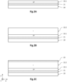
- FIG. 1A is a partial and schematic view, in cross-section, of a passivated planar photodiode 1 according to one embodiment, belonging to a matrix of photodiodes.
- the photodiodes 1 are made from germanium, and are reverse-polarized from the first surface 10a, while being isolated from each other by trenches filled with a p+ doped semiconductor material. They each comprise an intercalated semiconductor portion 27 located here between and in contact with a metal electrical polarization contact 32.1 and the first n+ doped region 11.
- a three-dimensional direct reference frame XYZ is defined, where the X and Y axes form a plane parallel to the main plane of the photodiode 1, and where the Z axis is oriented along the thickness of the detection portion 1 of the photodiode, from the second surface 10b in the direction of the first surface 10a.
- the photodiode 1 comprises a detection portion 10 extending along the Z axis between a first and a second reference surface 10a and 10b, parallel to each other and opposite to each other.
- the first surfaces 10a of the photodiodes are parallel between them, and the second surfaces 10b are also parallel to each other.
- the first surface 10a is defined by a part of the detection portion 10 where the first n+ doped region 11 and the intermediate region 13 are flush.
- the second surface 10b is opposite the first surface 10a along the Z axis.
- the maximum thickness of the detection portion 10, defined along the Z axis between the first and second surfaces 10a, 10b, is here substantially constant from one photodiode to another, for example is between a few hundred nanometers and a few microns, for example between approximately 1 ⁇ m and 5 ⁇ m. The thickness is chosen so as to obtain good absorption in the wavelength range of the light radiation to be detected.
- the detection portion 10 has a transverse dimension in the XY plane which can be between a few hundred nanometers and a few tens of microns, for example between approximately 1 ⁇ m and 20 ⁇ m.
- the detection portion 10 is made of a crystalline, preferably monocrystalline, germanium-based semiconductor material.
- germanium-based it is meant that the crystalline semiconductor material corresponds to germanium or is a compound formed of at least germanium.
- the photodiodes can be made, for example, of germanium Ge, silicon germanium SiGe, germanium tin GeSn, or even silicon germanium tin SiGeSn.
- the detection portion 10 is made of at least one layer made of germanium. It can thus be a layer or a substrate made of the same semiconductor material and have regions of different types of conductivity (homojunction) so as to form a PN or PIN junction. It can alternatively be a stack of sub-layers of different semiconductor materials (heterojunction), which are then formed based on germanium.
- the detection portion 10 is thus formed of a first n-type doped (n or n+) region 11, which is flush with the first surface 10a and forms an n-type doped well, and a second p+ doped region 12, which is flush with the second surface 10b.
- n or n+ n-type doped
- second p+ doped region 12 which is flush with the second surface 10b.
- An intermediate region 13 not intentionally doped (in the case of a PIN junction), or p-doped (in the case of a PN junction), is located between and in contact with the two doped regions 11 and 12, and surrounds the first n+ doped region 11 in the main plane.
- the semiconductor junction is of the PIN type, the first region 11 being n+ doped, the second region 12 p+ doped and the intermediate region 13 is intrinsic (not intentionally doped).
- the first n-type doped region 11 here extends from the first surface 10a and is surrounded by the intrinsic region 13 in the main plane. It is distant from the lateral edge 10c of the detection portion 10 in the XY plane, the lateral edge 10c being defined by the internal face of a p+ doped peripheral semiconductor portion 25. It thus forms an n+ doped well which is flush with the first surface 10a and is spaced of a non-zero distance from the lateral edge 10c as well as from the second surface 10b.
- the first n+ doped region 11 thus participates in delimiting the first surface 10a. It can have a doping which can be between 5.10 18 and 10 21 at/cm 3 approximately.
- the second p+ doped region 12 extends in the XY plane, flush with the second surface 10b, here from the lateral edge 10c. It extends along the Z axis from the second surface 10b. It may have a substantially uniform thickness along the Z axis and thus be flush with only a lower zone of the lateral edge 10c.
- the second p+ doped region 12 may have a p+ doped lateral region 14 which is continuously flush with the lateral edge 10c along the Z axis and extends over the entire periphery of the detection portion 10.
- the second p+ doped region 12 may have a doping which may be between approximately 10 18 and 10 19 at/cm 3 .
- the intermediate region 13 is located between the two n+ and p+ doped regions 11, 12, and surrounds the first n+ doped region 11 in the XY plane. It is here made of an intrinsic semiconductor material so as to form a PIN junction but can be weakly p-doped, to form a PN junction (cf. Fig. 1B ).
- the photodiode 1 here comprises a lower insulating layer 21, made of a dielectric material, covering the second surface 10b of the detection portion 10, as well as, as described later, the lower face of the p+-doped peripheral semiconductor portion 25.
- the lower insulating layer 21 may further be adapted to form an anti-reflection function with respect to the incident light radiation. It in fact forms the receiving face of the light radiation intended to be detected.
- the detection portion 10 of the photodiode 1 is here delimited laterally, in the XY plane, by a trench, preferably continuous, filled with a p+ doped semiconductor material, and forming a peripheral semiconductor portion 25, here p+ doped.
- the peripheral through portion 25 participates in electrically polarizing the photodiode 1, here from the side of the first surface 10a, and in pixelating the photodiode matrix (optical isolation). It extends here over the entire thickness of the detection portion 10 to open onto the lower insulating layer 21, but alternatively, it may not open onto the lower insulating layer 21 and may end in the second p+ doped region 12.
- the internal face of this p+ doped peripheral semiconductor portion 25 then defines the lateral edge 10c of the detection portion 10.
- the semiconductor material is preferably made from silicon, for example amorphous silicon, polycrystalline silicon, silicon germanium, or can even be made from amorphous germanium.
- An upper insulating layer 23 covers the first surface 10a of the photodiode 1, and makes it possible to electrically insulate the metal contacts 32.1 and 32.2. It is thus in contact with the first n+ doped region 11 as well as the intermediate region 13. It is made of a dielectric material, such as silicon oxide, silicon nitride, or silicon oxynitride. Other dielectric materials can be used, such as hafnium or aluminum oxide, or even aluminum nitride, among others. It has a thickness, for example, between 50nm and 500nm.
- the detection portion 10 advantageously comprises a p+ doped lateral region 14 located at the lateral edge 10c.
- This lateral region 14 has a doping level higher than that of the intermediate region 13 when it is doped.
- the p+ doped lateral region 14 is flush with the lateral edge 10c and is in contact with the p+ doped peripheral semiconductor portion 25.
- the polarization of the second p+ doped region 12 is improved to the extent that the contact surface with the p+ doped peripheral semiconductor portion 25 is increased.
- this p+ doped lateral region 14 makes it possible to prevent the space charge zone of the photodiode 1 from extending as far as the lateral edge 10c.
- the contribution of this zone (potentially not free from defects linked to the production of the trenches) to the dark current is limited. This improves the performance of photodiode 1.
- the detection portion 10 is made from germanium, for example is made from germanium, and the p+-doped peripheral semiconductor portion 25 is made from silicon, for example doped polycrystalline silicon.
- the detection portion 10 then advantageously comprises a lateral zone 15 made from silicon germanium.
- the lateral zone 15 is flush with the lateral edge 10c and is in contact with the p+-doped peripheral semiconductor portion 25.
- the lateral zone 15 has a bandgap energy greater than that of the detection portion 10 made from germanium.
- This lateral “gap opening” makes it possible to reduce the sensitivity of the photodiode 1 to defects present near the trenches. This also improves the performance of the photodiode 1.
- the photodiode 1 comprises an intercalated semiconductor portion 27, arranged on and in contact with the first n+ doped region 11. It is spaced by a non-zero distance from the peripheral semiconductor portions 25 in the XY plane and is here surrounded by the upper insulating layer 23. It is made of a crystalline semiconductor material doped here of the n+ type, which has a natural lattice parameter equal to within 1%, and preferably to within 0.5%, of that of the crystalline semiconductor material of the detection portion 10, here germanium, and has a band gap energy greater by at least 0.5eV than that of the crystalline semiconductor material of the detection portion 10 (germanium).
- the intercalated semiconductor portion 27 can thus be made of a III-V binary or ternary compound, such as GaAs, AlAs, GaAlAs, GaInP, among others.
- the intermediate semiconductor portion 27 is advantageously located in a notch formed in the first surface 10a of the detection portion. 10, which makes it possible to reduce or even avoid the presence of structural defects (dislocations) in the intercalated portion 27, as described later. Alternatively, it can rest on the first surface 10a which is then continuously flat (no notch).
- the size in the XY plane of the intercalated semiconductor portion 27 depends on the size of the photodiode 1: for a photodiode with a pitch of 5 ⁇ m, it can be between approximately 0.5 and 4 ⁇ m (and preferably less than 2 ⁇ m), and for a pitch of 10 ⁇ m, it can be between approximately 1 and 9 ⁇ m.
- the intercalated semiconductor portion 27 comprises n-type dopants identical to those present in the first n+ doped region 11, insofar as, as explained below, the formation of the first region 11 is carried out by diffusion of the dopants through the intercalated semiconductor portion 27 (cf. fig.2A to 2L ) or initially contained in the intercalated semiconductor portion 27 ( fig.3A to 3C ).
- the photodiode 1 further comprises metal contacts 32.1, 32.2 allowing it to be reverse-biased from the side of the first surface 10a.
- a metal contact 32.1 is here arranged on and in contact with the intermediate semiconductor portion 27, and allows the first n+ doped region 11 to be electrically polarized.
- a metal contact 32.2 is here arranged on and in contact with the peripheral semiconductor portion 25, and allows the second p+ doped region 12 to be electrically polarized.
- the metal contacts 32.1, 32.2 are here electrically isolated from each other in the XY plane by the upper insulating layer 23 and by a passivation dielectric layer 29.
- the photodiode 1 is intended to be reverse biased, for example by applying a negative electrical potential to the p+ doped peripheral semiconductor portion 25 and by bringing the first n+ doped region 11 to ground.
- the photodiode 1 may have dimensions in the XY plane of between approximately 1 ⁇ m and 100 ⁇ m.
- the thickness of the second p+ doped region 12 may be between approximately 20 nm and 500 nm.
- the thickness of the intrinsic region 13 may be between approximately 0.7 ⁇ m and 2.5 ⁇ m when the photodiode 1 is intended to detect light radiation in the SWIR or near infrared (NIR) range.
- the first n+ doped region 11 may have a thickness of between approximately 10 nm and 600 nm.
- the dielectric layers 23 and 29 may together have a thickness enabling the upper face of the photodiode 1 to be completely covered, for example between approximately 10 nm and 600 nm, and the thickness of the lower insulating layer 21 may be between approximately 50 nm and 1 ⁇ m.
- the photodiode 1 has improved performance compared to the examples of the prior art mentioned previously. Indeed, the photodiode 1, by the presence of the intermediate semiconductor portion 27 located between the metal contact 32.1 and the n-doped germanium 11, does not have a metal contact on the n-doped germanium
- the intercalated semiconductor portion 27, which is in contact with the first n+ doped region 11, is made of a semiconductor material with a band gap energy at least 0.5eV higher than that of germanium, which makes it possible to reduce the dark current of the photodiode 1 on the one hand, and to reduce the sensitivity of the photodiode 1 to defects possibly present near the notch in which the intercalated semiconductor portion 27 is located.
- FIG. 1B is a schematic and partial view, in cross-section, of a photodiode 1 according to an alternative embodiment.
- the photodiode 1 differs from that illustrated in the fig.1A in particular in that the intermediate region 13 is weakly p-doped (PN junction), and in that an upper semiconductor portion 28 is located between and in contact with the central metal contact 32.1 and the intermediate semiconductor portion 27.
- PN junction weakly p-doped
- the intercalated semiconductor portion 27 rests on and in contact with the detection portion 10. It is thus in contact with the first n+ doped region 11. It is made of a crystalline semiconductor material having the properties mentioned above in terms of band gap energy and absence of lattice mismatch with the germanium of the detection portion 10. As indicated below, it was made by epitaxy from germanium and in an unintentionally doped manner.
- the upper semiconductor portion 28 therefore rests on and in contact with the intercalary semiconductor portion 27. It is spaced from the peripheral semiconductor portion 25 and the metal contacts 32.2 in the XY plane by a non-zero distance. This lateral space is filled here by the passivation dielectric layer 29.
- the upper semiconductor portion 28 is made of an n+ doped semiconductor material, with dopants capable of n+ doping the germanium to form the first n+ doped region 11, here with phosphorus or arsenic.
- the upper semiconductor portion 28 is a reservoir of dopants intended to diffuse, during diffusion annealing, through the intercalary semiconductor portion 27 to join the germanium and form the first n+ doped region 11. It is preferably made from polycrystalline silicon, but other polycrystalline materials can of course be used.
- the metal contact 32.1 is here arranged on and in contact with the upper semiconductor portion 28. It makes it possible to electrically polarize the first n+ doped region 11 via the upper semiconductor portion 28 then the intermediate semiconductor portion 27.
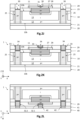
- FIGS. 2A to 2L are schematic and partial views, in cross-section, of different stages of a method of manufacturing a photodiode according to the example of the fig.1B .
- This method has the particular advantage of producing the metal contacts 32.1 and 32.2 simultaneously. It also has the advantage of not doping the intercalated semiconductor portion 27 during growth (controlling the diffusion of the dopants can be tricky) or by ion implantation (which can create defects in the intercalated semiconductor portion 27).
- the photodiodes 1 are made of germanium and have a PIN junction, and are adapted to detect infrared radiation in the SWIR range.
- the photodiodes 1 are planar and passivated, and are reverse biased from the first surface 10a, and here by means of a control chip 40 hybridized to the photodiode matrix 1.
- a first semiconductor sub-layer 22.1 of monocrystalline germanium is produced.
- the first semiconductor sub-layer 22.1 is secured to a support layer 20, here made of silicon, via a lower insulating layer 21, here made of silicon oxide.
- This stack takes the form of a GeOI substrate (for Germanium On Insulator, in English).
- This stack is preferably produced using the method described in the publication of Reboud et al. entitled Structural and optical properties of 200mm germanium-on-insulator (GeOI) substrates for silicon photonics applications, Proc. SPIE 9367, Silicon Photonics X, 936714 (February 27, 2015 ).
- Such a method has the advantage of producing a germanium 22.1 semiconductor sub-layer having a total absence or a low rate of structural defects such as dislocations.
- the germanium may be unintentionally doped or be doped, for example p-type.
- the semiconductor sub-layer 22.1 may have a thickness of between approximately 100nm and 500nm, for example equal to approximately 300nm, and may be covered with a protective layer (not shown) made of a silicon oxide.
- the lower insulating layer 21 (BOX, for Buried Oxide, in English) may have a thickness of between 50nm and 1 ⁇ m, for example between 100nm and 500nm, and advantageously provides an anti-reflection function.
- the first sub-layer 22.1 is then doped with p+-doped germanium by ion implantation of a dopant such as boron or gallium, when the first sub-layer 22.1 was initially made of intrinsic germanium.
- a dopant such as boron or gallium
- the protective layer if any, was previously removed by surface cleaning, and the first sub-layer 22.1 of germanium can be coated with a pre-implantation oxide layer (not shown) with a thickness of a few tens of nanometers, for example equal to 20nm.
- the 22.1 germanium sub-layer then has a doping level of between 10 18 and 10 20 at/cm 3 approximately.
- a diffusion annealing of the dopant can then be carried out under nitrogen, for a few minutes to a few hours, for example 1h, at a temperature which can be between 600°C and 800°C, for example equal to 800°C. This annealing can not be carried out when the 22.1 sub-layer was doped at growth.
- Another way of manufacturing this p+ layer is by epitaxy of a layer of germanium doped with boron in situ between 10 18 and 10 19 at/cm 3 approximately on an intrinsic germanium sub-layer. This epitaxy can be done between 400 and 800°C but preferably at 400°C.
- a second semiconductor sub-layer 22.2 of germanium is produced by epitaxy from the first sub-layer 22.1.
- the two sub-layers 22.1, 22.2 are intended to form the coplanar detection portions 10 made of germanium of the photodiode matrix 1.
- the second sub-layer 22.2 is formed by epitaxy, for example by chemical vapor deposition (CVD) and reduced pressure chemical vapor deposition (RPCVD) or by any other epitaxy technique. Annealing may be carried out to reduce the dislocation rate in the sub-layer 22.2.
- the pre-implementation oxide layer, if any, has been previously removed by surface cleaning.
- the second sub-layer 22.2 of germanium is here intrinsic, that is to say not intentionally doped insofar as it is desired to produce a PIN junction. It is intended to form the light absorption zone of the photodiodes 1. Its thickness depends on the wavelength range of the light radiation to be detected in the case of a photodiode 1. In the context of SWIR photodiodes, the sub-layer 22.2 of intrinsic germanium has a thickness for example between 0.5 ⁇ m and 3 ⁇ m, preferably equal to 1.5 ⁇ m.
- an upper insulating layer 23 is deposited so as to continuously cover the upper face of the second sub-layer 22.2, that is to say so as to cover the detection portions 10 of the photodiodes 1.
- the upper insulating layer 23 is made of a dielectric material, for example a silicon oxide, nitride or oxynitride. Cleaning of the upper face of the second sub-layer 22.2 may have been carried out beforehand.
- the upper insulating layer 23 may have a thickness of between 10nm and 600nm.
- the trenches 24 intended to pixelate the photodiodes 1 and to participate in their reverse electrical polarization are produced by photolithography and etching (by means of the peripheral semiconductor portions 25 which will then be produced).
- a localized etching of the upper insulating layer 23, of the intrinsic germanium sub-layer 22.2, and of the germanium sub-layer 22.1 are thus carried out.
- Each trench 24 thus preferably extends continuously around a photodiode 1.
- a plurality of detection portions 10 are thus obtained, separated from each other by a continuous trench 24.
- the trenches 24 have a transverse dimension (width) in the XY plane which can be between 300nm and 2 ⁇ m, for example equal to 1 ⁇ m.
- the detection portions 10 can thus have a shape in the XY plane, for example circular, oval, polygonal, for example square, or any other shape.
- the peripheral semiconductor portions 25 are then produced.
- a doped semiconductor material is deposited so as to fill the trenches 24.
- the semiconductor material is preferably a silicon-based material, for example amorphous silicon, polycrystalline silicon, silicon germanium, or even amorphous germanium.
- the semiconductor material is doped p+ with boron or gallium, with a dopant concentration of the order of approximately 10 19 to 10 20 at/cm 3 . Thus, the doped semiconductor material comes into contact with the lateral edge 10c via the trench 24.
- a chemical mechanical polishing (CMP) step is then carried out, with a stop on the upper face of the upper insulating layer 23, to remove the excess semiconductor material and planarize the upper face formed by the upper insulating layer 23 and the semiconductor material of the peripheral semiconductor portion 25.
- CMP chemical mechanical polishing
- a dielectric layer is deposited so as to cover the upper surface of the peripheral semiconductor portions 25 (this increases the thickness of the upper insulating layer 23 which thus covers the portions 25). Then, by photolithography and etching, a through opening 26.1 is produced within the upper insulating layer 23 to open onto the detection portion 10, opposite a central zone located at a distance from the peripheral semiconductor portions 25 in the XY plane.
- the width or diameter of the through opening 26.1 depends in particular on the desired width of the first n+ doped region. It can be between 0.3 ⁇ m and 5 ⁇ m for example.
- the through opening 26.1 also forms a notch within the detection portion 10, for example with a depth of around a hundred nanometers.
- an intercalated semiconductor portion 27 is produced, located opposite the central zone of the detection portion 10 and in contact with it.
- the intercalated semiconductor portion 27 is produced by epitaxy here from the germanium of the detection portion, for example by molecular beam epitaxy (MBE, Molecular Beam Epitaxy, in English). It is made of a semiconductor material crystalline which has, on the one hand, a lattice parameter almost identical to that of germanium, that is to say that its natural lattice parameter is equal to that of germanium to at most 1.0%, and preferably to at most 0.5%; and on the other hand, a band gap energy Eg higher (that is to say strictly higher) than that Eg Ge of the germanium of the detection portion.
- MBE molecular beam epitaxy
- the intercalated semiconductor portion 27 is made of AlAs or GaAs (stoichiometric compounds, i.e. the proportion of the two elements is identical, whose natural lattice parameter is 5.6605 ⁇ for AlAs and 5.653 ⁇ for GaAs, which corresponds respectively to a deviation of 0.044% and 0.088% with the natural lattice parameter of 5.658 ⁇ of germanium.
- the band gap energy is 2.12eV for AlAs and 1.424eV for GaAs, which is much higher than the 0.67eV of germanium.
- Other semiconductor compounds, for example ternary may also be suitable, such as for example GaAlAs and GaInP depending on the proportions of the different chemical elements.
- the intercalated semiconductor portion 27 is intrinsic, i.e. not intentionally doped.
- the formation of the first n+ doped region 11 will be obtained by diffusion of germanium dopants (e.g. phosphorus or arsenic) from a dopant reservoir (the upper semiconductor portion 28) through the intercalated semiconductor portion 27).
- germanium dopants e.g. phosphorus or arsenic
- an upper semiconductor portion 28 is produced, forming the reservoir of n-type dopants intended to diffuse into the detection portion through the intermediate semiconductor portion 27 to ultimately obtain the first n+ doped region 11. It is produced from an n+ doped semiconductor material, for example polysilicon or polycrystalline silicon germanium. However, it is advantageously produced from a material identical to that of the peripheral semiconductor portion, for example here polysilicon, so as to simplify the production of the metal contacts 32.1 and 32.2.
- the upper semiconductor portion 28 is made of polysilicon doped n+ with phosphorus or arsenic, produced by low-pressure chemical vapor deposition (LPCVD) between 400°C and 650°C for example. It has a size in the XY plane preferably greater than that of the intercalary semiconductor portion 27, and a thickness of for example between 50nm and 200nm.
- LPCVD low-pressure chemical vapor deposition
- a diffusion and activation annealing of the dopants is then carried out, for example between 500°C and 800°C and for approximately 10 to 60 min.
- the dopants phosphorus or arsenic
- the dopants diffuse through the intercalated semiconductor portion 27 then into the detection portion 10.
- a first n+ doped region 11 is thus obtained which extends in contact with the intercalated semiconductor portion 27, both along the Z axis and in the XY plane.
- the intercalated semiconductor portion 27 was epitaxially grown in a notch 26.2 of the detection portion 10 makes it possible to reduce the number of structural defects (dislocations) in the intercalated semiconductor portion 27 or even to avoid them. This results in a crystalline material of better crystalline quality, which improves the performance of the photodiode.
- a passivation dielectric layer 29 is deposited so as to cover the upper semiconductor portion 28.
- the dielectric layer can be deposited at 400°C and be made of a dielectric material such as a silicon oxide, nitride or oxynitride, an aluminum oxide or nitride, a hafnium oxide, among others. It can have a thickness of, for example, between 200nm and 1000nm.
- a CMP-type planarization step is then carried out.
- Through openings 30 are then made through the dielectric layers 23, 29 so as to open onto an upper surface of the peripheral semiconductor portion 25 (to then make the metal contact 32.2) and onto an upper surface of the upper semiconductor portion 28 (to then make the metal contact 32.1).
- These through openings 30 may have a size in the XY plane of between 0.1 ⁇ m and 1 ⁇ m, preferably between 0.3 ⁇ m and 1 ⁇ m. They may be made by plasma etching with an etching stop on the polysilicon surfaces of the upper semiconductor portion 28 and the peripheral semiconductor portion 25.
- the upper portion 28 and the peripheral portion 25 are made of the same material, here silicon, makes it possible to make the metal contacts 32.1 and 32.2 simultaneously, thus simplifying the manufacturing process.
- a silicided zone 31 is preferably produced on the upper surface of the upper semiconductor portion 28, and a silicided zone 31 on the upper surface of the peripheral semiconductor portion 25.
- a thin layer of the type formed by a Ni/TiN stack with thicknesses of 9nm and 10nm is deposited at the bottom of the through openings 30, 30 by physical vapor deposition (PVD), followed by a siliciding annealing between approximately 300°C and 350°C for approximately 10 to 30s.
- PVD physical vapor deposition
- the unreacted Ni and TiN is then removed, and then a second siliciding annealing is carried out between approximately 400°C and 450°C for approximately 10 to 30s.
- the central 32.1 and lateral 32.2 metal contacts are then produced.
- a thin bonding layer 33 formed from a Ti/TiN/Cu type stack is deposited by chemical deposition in the value phase in the through openings 30.1, 30.2, and the empty space is filled with copper 34 deposited by electrolysis.
- a CMP type planarization step is then carried out with a stop on the oxide of the dielectric passivation layer 29.
- the dielectric passivation layer 29 and the metal contacts 32.1 and 32.2 together have the same planar upper face.
- the hybridization of the optoelectronic stack thus obtained is carried out on a control chip 40.
- the connection face of the control chip 40 can thus be coated with an insulating layer 41, made of a dielectric material, crossed by metal contacts 42.
- the photodiode matrix 1 and the control chip 40 are thus assembled by hybrid molecular adhesion, by contact of the faces formed by the metal contacts and the insulating layers.
- a bonding annealing can be carried out so as to increase the surface bonding energy between the two faces in contact.
- the support layer 20 is then removed, for example by abrasion ( grinding, in English), so as to expose the lower insulating layer 21. This thus forms the receiving face of the light radiation to be detected, and advantageously provides an antireflection function.
- the manufacturing method thus makes it possible to obtain one or more passivated photodiodes 1, each comprising an interposed semiconductor portion 27 in contact with the detection portion 10, the properties of which in terms of mesh parameters and band gap energy make it possible to avoid having to make a metal contact directly on the n-doped germanium, such a contact being either of the rectifier type or of the ohmic but highly resistive type.
- One or more photodiodes 1 are thus produced having improved performance, in particular in terms of low-frequency noise (as indicated previously).
- FIGS. 3A to 3C are schematic and partial views, in cross-section, of different stages of a method of manufacturing a photodiode 1 according to the example of the fig.1A .
- Photodiode 1 is different from the one illustrated in the fig.1B essentially in that it does not include an upper semiconductor portion 28. Also, the metal contact 32.1 is on and in contact with the intermediate semiconductor portion 27.
- the first n+ doped region 11 is produced by diffusion of dopants from the intermediate semiconductor portion 27 which itself forms the dopant reservoir (and not from the upper semiconductor portion 28, as in the Figures 2A to 2L ).
- the intermediate semiconductor portion 27 is produced by epitaxial growth directly from the detection portion 10. This step is similar to that of the fig.2G and is distinguished in that the intercalated semiconductor portion 27 is n+ doped with dopants suitable for n-doping the germanium of the detection portion 10, for example here with phosphorus, arsenic, or even silicon or zinc.
- the intercalated semiconductor portion 27 is doped during growth and not by ion implantation, to avoid any degradation of the crystalline quality of the material.
- the dopants do not modify the properties of the material of the portion intercalated semiconductor 27 in terms of lattice parameter.
- the band gap energy remains at least 0.5eV higher than that of the germanium of the detection portion 10.
- the epitaxy temperature is controlled to limit possible diffusion of the dopants in the detection portion 10.
- the first n+ doped region 11 is produced by performing a diffusion and activation annealing of the dopants.
- the temperature and duration of the annealing can be similar to those mentioned previously, in connection with the fig.2I .
- the dopants diffuse from the intercalated semiconductor portion 27 into the detection portion 10, which forms the first n+ doped region 11.
- the metal contacts 32.1 and 32.2 are produced.
- a through opening is produced in the insulating layers 23 and 29 which opens onto the peripheral semiconductor portion 25, then the silicided zone 31 is produced.
- a through opening is produced in the insulating layer 29 which opens onto the intermediate semiconductor portion 27.
- a thin bonding layer 33 is deposited in the openings and then the free space is filled with copper 34. This gives the metal contacts 32.1 and 32.2.
Landscapes
- Light Receiving Elements (AREA)
- Electrodes Of Semiconductors (AREA)
Claims (15)
- Photodiode (1), umfassend:∘einen Detektionsabschnitt (10), der eine erste Oberfläche (10a) und eine zweite Oberfläche (10b) aufweist, die entgegengesetzt zueinander und parallel zu einer Hauptebene sind, und der aus einem kristallinen ersten Halbleitermaterial auf Germaniumbasis ausgeführt ist, umfassend:• eine erste Region (11), die n-dotiert ist und bündig zu der ersten Oberfläche (10a) ist;• eine zweite Region (12), die p-dotiert ist und bündig zu der zweiten Oberfläche (10b) ist;• eine Zwischenregion (13), die zwischen der ersten Region (11) und der zweiten Region (12) gelegen ist und die erste Region (11) in der Hauptebene umgibt;∘ einen umfänglichen Halbleiterabschnitt (25), der aus einem p-dotierten zweiten Halbleitermaterial ausgeführt ist, den Detektionsabschnitt (10) in der Hauptebene umgibt und in Kontakt mit der zweiten Region (12) gelangt;∘ einen dazwischen liegenden Halbleiterabschnitt (27), der auf und in Kontakt mit der ersten Region (11) des Detektionsabschnitts (10) angeordnet ist;∘ Metallkontakte (32.1, 32.2), die auf der Seite der ersten Oberfläche (10a) angeordnet sind und dazu angepasst sind, zum einen die erste Region (11) über den dazwischen liegenden Halbleiterabschnitt (27) und zum anderen die zweite Region (12) über den umfänglichen Halbleiterabschnitt (25) elektrisch zu polarisieren;∘ dadurch gekennzeichnet, dass der dazwischen liegende Halbleiterabschnitt (27) aus einem kristallinen dritten Halbleitermaterial ausgeführt ist, aufweisend:• einen natürlichen Gitterparameter, der bis auf 1 % gleich einem natürlichen Gitterparameter des ersten Halbleitermaterials auf Germaniumbasis ist;• eine Bandlückenenergie, die um mindestens 0,5 eV größer als die des ersten Halbleitermaterials auf Germaniumbasis ist.
- Photodiode (1) nach Anspruch 1, wobei der dazwischen liegende Halbleiterabschnitt (27) n-Dotierungsstoffe umfasst, die identisch mit den in der ersten Region (11) vorhandenen sind.
- Photodiode (1) nach Anspruch 1 oder 2, wobei der dazwischen liegende Halbleiterabschnitt (27) aus einer kristallinen III-V-Halbleiterverbindung ausgeführt ist.
- Photodiode (1) nach Anspruch 3, wobei der dazwischen liegende Halbleiterabschnitt (27) aus AlAs oder aus GaAs ausgeführt ist.
- Photodiode (1) nach einem der Ansprüche 1 bis 4, wobei der dazwischen liegende Halbleiterabschnitt (27) in einem Ausschnitt der ersten Oberfläche (10a) des Detektionsabschnitts (10) gelegen ist, so dass der dazwischen liegende Halbleiterabschnitt (27) in der Hauptebene von der ersten Region (11) umgeben ist.
- Photodiode (1) nach einem der Ansprüche 1 bis 5, wobei einer der Metallkontakte (32.1), zentraler Metallkontakt genannt, auf und in Kontakt mit dem dazwischen liegenden Halbleiterabschnitt (27) gelegen ist.
- Photodiode (1) nach einem der Ansprüche 1 bis 5, umfassend einen oberen Halbleiterabschnitt (27), der auf und in Kontakt mit dem dazwischen liegenden Halbleiterabschnitt (27) gelegen ist und aus einem n-dotierten Halbleitermaterial mit Dotierungsstoffen ausgeführt ist, die identisch mit denen des dazwischen liegenden Halbleiterabschnitts (27) und der ersten Region (11) sind.
- Photodiode (1) nach Anspruch 7, wobei einer der Metallkontakte (32.1), zentraler Metallkontakt genannt, auf und in Kontakt mit dem oberen Halbleiterabschnitt (28) gelegen ist.
- Photodiode (1) nach Anspruch 7 oder 8, wobei der obere Halbleiterabschnitt (28) aus einem Material ausgeführt ist, das identisch mit dem des umfänglichen Halbleiterabschnitts (25) ist.
- Photodiode (1) nach einem der Ansprüche 7 bis 9, wobei der obere Halbleiterabschnitt (27) und der umfängliche Halbleiterabschnitt (25) aus einem Halbleitermaterial auf Siliziumbasis ausgeführt sind und umfassend einen silizidierten oberen Bereich (31) in Kontakt mit den Metallkontakten (32.1, 32.2).
- Verfahren zur Herstellung einer Photodiode nach einem der vorhergehenden Ansprüche, umfassend die folgenden Schritte∘ Ausführen eines Schichtsystems, umfassend eine erste Teilschicht (22.1), die dazu bestimmt ist, die zweite Region (12) zu bilden, und eine zweite Teilschicht (22.2), die dazu bestimmt ist, die dazwischen liegende Region (13) zu bilden;∘Ausführen einer oberen isolierenden Schicht (23), die das Schichtsystem bedeckt;∘ Ausführen des umfänglichen Halbleiterabschnitts (25) durch das Schichtsystem und die obere isolierende Schicht (23) hindurch, um auf der ersten Teilschicht (22.1) zu münden;∘ Ausführen des dazwischen liegenden Halbleiterabschnitts (27) durch Epitaxie ausgehend von der zweiten Teilschicht (22.2) des Schichtsystems durch eine Öffnung (26.1) der oberen isolierenden Schicht (23) hindurch.
- Verfahren zur Herstellung nach Anspruch 11, umfassend, vor dem Schritt des Ausführens des dazwischen liegenden Halbleiterabschnitts (27), einen Schritt des Ausführens eines Ausschnitts (26.2) in der zweiten Teilschicht (22.2) des Schichtsystems durch die Öffnung (26.1) hindurch, gefolgt von der Epitaxie des dazwischen liegenden Halbleiterabschnitts (27) in dem Ausschnitt (26.2).
- Verfahren zur Herstellung nach Anspruch 11 oder 12, wobei der dazwischen liegende Halbleiterabschnitt (27) bei seiner Epitaxie nicht absichtlich dotiert wird, wobei das Verfahren die folgenden Schritte umfasst:∘ Ausführen des n-dotierten oberen Halbleiterabschnitts (28);∘ Glühen, das dazu angepasst ist, die Diffusion der in dem oberen Halbleiterabschnitt (28) enthaltenen Dotierungsstoffe durch den dazwischen liegenden Halbleiterabschnitt (27) zu veranlassen, um die erste Region (11) in dem Detektionsabschnitt (10) zu bilden.
- Verfahren zur Herstellung nach Anspruch 13, wobei der obere Halbleiterabschnitt (28) und der umfängliche Halbleiterabschnitt (25) aus einem selben Material auf Siliziumbasis ausgeführt sind, wobei das Verfahren ferner den folgenden Schritt umfasst:∘ gleichzeitiges Ausführen der Metallkontakte (32.1, 32.2), einen (32.1) in Kontakt mit dem oberen Halbleiterabschnitt (28) und den anderen (32.2) in Kontakt mit dem umfänglichen Halbleiterabschnitt (25).
- Verfahren zur Herstellung nach Anspruch 11 oder 12, wobei der dazwischen liegende Halbleiterabschnitt (27) bei seiner Epitaxie n-dotiert wird, wobei das Verfahren den folgenden Schritt umfasst:∘Ausführen der Metallkontakte (32.1, 32.2), einen (32.1) in Kontakt mit dem dazwischen liegenden Halbleiterabschnitt (27) und den anderen (32.2) in Kontakt mit dem umfänglichen Halbleiterabschnitt (25).
Applications Claiming Priority (2)
| Application Number | Priority Date | Filing Date | Title |
|---|---|---|---|
| FR2101290A FR3119711B1 (fr) | 2021-02-11 | 2021-02-11 | Photodiode germanium à contacts métalliques optimisés |
| PCT/EP2022/053073 WO2022171650A1 (fr) | 2021-02-11 | 2022-02-09 | Photodiode germanium a contacts metalliques optimises |
Publications (2)
| Publication Number | Publication Date |
|---|---|
| EP4292136A1 EP4292136A1 (de) | 2023-12-20 |
| EP4292136B1 true EP4292136B1 (de) | 2025-04-23 |
Family
ID=75690433
Family Applications (1)
| Application Number | Title | Priority Date | Filing Date |
|---|---|---|---|
| EP22704381.7A Active EP4292136B1 (de) | 2021-02-11 | 2022-02-09 | Germanium-photodiode mit optimierten metallkontakten |
Country Status (5)
| Country | Link |
|---|---|
| US (1) | US20240105864A1 (de) |
| EP (1) | EP4292136B1 (de) |
| CN (1) | CN116830280A (de) |
| FR (1) | FR3119711B1 (de) |
| WO (1) | WO2022171650A1 (de) |
Families Citing this family (1)
| Publication number | Priority date | Publication date | Assignee | Title |
|---|---|---|---|---|
| FR3114440B1 (fr) * | 2020-09-21 | 2022-08-19 | Commissariat Energie Atomique | Photodiode passivée comportant une portion périphérique ferroélectrique |
Family Cites Families (8)
| Publication number | Priority date | Publication date | Assignee | Title |
|---|---|---|---|---|
| FI20021255A7 (fi) * | 2002-06-27 | 2003-12-28 | Metorex Int Oy | Suoraan konversioon perustuva kuvaava röntgendetektori ja sellaista käyttävä kuvausjärjestely |
| US20070170536A1 (en) * | 2006-01-25 | 2007-07-26 | Sharp Laboratories Of America, Inc. | Liquid phase epitaxial GOI photodiode with buried high resistivity germanium layer |
| US9082849B2 (en) * | 2011-09-30 | 2015-07-14 | The Institute of Microelectronics Chinese Academy of Science | Semiconductor structure and method for manufacturing the same |
| US8778725B1 (en) * | 2011-10-25 | 2014-07-15 | SiFotonics Technologies Co, Ltd. | Avalanche photodiode with special lateral doping concentration |
| CN103426968A (zh) * | 2012-05-14 | 2013-12-04 | 杜邦太阳能有限公司 | 增强导电氧化物层雾度的方法及透明导电氧化物透明基底 |
| JP6785057B2 (ja) * | 2016-05-02 | 2020-11-18 | ルネサスエレクトロニクス株式会社 | 半導体装置およびその製造方法 |
| FR3089062A1 (fr) | 2018-11-23 | 2020-05-29 | Commissariat A L'energie Atomique Et Aux Energies Alternatives | procede de fabrication d’au moins une photodiode planaire passivee a courant d’obscurité reduit |
| FR3089348B1 (fr) * | 2018-11-30 | 2020-10-30 | Commissariat Energie Atomique | procede de fabrication d’une matrice de diodes a base de germanium et a faible courant d’obscurité |
-
2021
- 2021-02-11 FR FR2101290A patent/FR3119711B1/fr active Active
-
2022
- 2022-02-09 WO PCT/EP2022/053073 patent/WO2022171650A1/fr not_active Ceased
- 2022-02-09 US US18/264,502 patent/US20240105864A1/en active Pending
- 2022-02-09 CN CN202280014269.8A patent/CN116830280A/zh active Pending
- 2022-02-09 EP EP22704381.7A patent/EP4292136B1/de active Active
Also Published As
| Publication number | Publication date |
|---|---|
| WO2022171650A1 (fr) | 2022-08-18 |
| FR3119711A1 (fr) | 2022-08-12 |
| CN116830280A (zh) | 2023-09-29 |
| FR3119711B1 (fr) | 2023-01-13 |
| US20240105864A1 (en) | 2024-03-28 |
| EP4292136A1 (de) | 2023-12-20 |
Similar Documents
| Publication | Publication Date | Title |
|---|---|---|
| EP3657556B1 (de) | Herstellungsverfahren mindestens einer passivierten planaren fotodiode mit reduziertem dunkelstrom | |
| EP3660930B1 (de) | Herstellungsverfahren einer fotodiodenmatrix auf germaniumbasis und mit schwachem dunkelstrom | |
| EP3971995B1 (de) | Passivierte fotodiode mit einem ferroelektrischen peripheren teil | |
| EP3806167B1 (de) | Verfahren zur herstellung mindestens einer planaren fotodiode unter spannung | |
| EP3012876B1 (de) | Herstellungsverfahren einer rauscharmen fotodiode | |
| EP3782205A1 (de) | Optoelektronische vorrichtung mit einer durch eine inverse piezoelektrische wirkung unter zugspannung stehenden diode | |
| EP4184594B1 (de) | Germanium-photodiode mit reduziertem dunkelstrom mit einem auf sige/ge basierenden peripheren zwischenteil | |
| FR2694134A1 (fr) | Procédé de fabrication d'une diode photovoltaïque et diode à structure plane. | |
| FR2992471A1 (fr) | Structure semiconductrice comportant une zone absorbante placee dans une cavite focalisante | |
| EP3396720B1 (de) | Herstellungsverfahren einer fotodiodenmatrix mit mesa-strukturen | |
| EP3011602B1 (de) | Solarzelle mit einem silikonheteroübergang | |
| EP4292136B1 (de) | Germanium-photodiode mit optimierten metallkontakten | |
| EP4354524B1 (de) | Planare photodiode auf germaniumbasis mit einer kompressiven peripheren seitlichen zone | |
| WO2018007529A1 (fr) | Procédé de fabrication de photodétecteur comprenant un empilement de couches superposées | |
| EP4386873B1 (de) | Stromunterstützter photonischer demodulator mit vertikal angeordneten dotierten modulations- und sammelregionen in einer zone unter druckbeanspruchung | |
| EP4379821B1 (de) | Stromunterstützter photonischer demodulator mit verbesserter leistung und zwischenelektroden | |
| EP3764403B1 (de) | Herstellung einer fotosensiblen vorrichtung mit halbleiter | |
| FR3162870A1 (fr) | Démodulateur photonique assisté par courant à consommation d’énergie réduite | |
| EP3671843A1 (de) | Herstellungsverfahren einer vielzahl von dioden aus einem lesesubstrat | |
| EP0577497A1 (de) | Vertikaler JFET-Transistor mit geringer Gate/Substrat-Kapazität und Verfahren zu seiner Herstellung |
Legal Events
| Date | Code | Title | Description |
|---|---|---|---|
| STAA | Information on the status of an ep patent application or granted ep patent |
Free format text: STATUS: UNKNOWN |
|
| STAA | Information on the status of an ep patent application or granted ep patent |
Free format text: STATUS: THE INTERNATIONAL PUBLICATION HAS BEEN MADE |
|
| PUAI | Public reference made under article 153(3) epc to a published international application that has entered the european phase |
Free format text: ORIGINAL CODE: 0009012 |
|
| STAA | Information on the status of an ep patent application or granted ep patent |
Free format text: STATUS: REQUEST FOR EXAMINATION WAS MADE |
|
| 17P | Request for examination filed |
Effective date: 20230719 |
|
| AK | Designated contracting states |
Kind code of ref document: A1 Designated state(s): AL AT BE BG CH CY CZ DE DK EE ES FI FR GB GR HR HU IE IS IT LI LT LU LV MC MK MT NL NO PL PT RO RS SE SI SK SM TR |
|
| DAV | Request for validation of the european patent (deleted) | ||
| DAX | Request for extension of the european patent (deleted) | ||
| RAP3 | Party data changed (applicant data changed or rights of an application transferred) |
Owner name: COMMISSARIAT A L'ENERGIE ATOMIQUE ET AUX ENERGIESALTERNATIVES |
|
| GRAP | Despatch of communication of intention to grant a patent |
Free format text: ORIGINAL CODE: EPIDOSNIGR1 |
|
| STAA | Information on the status of an ep patent application or granted ep patent |
Free format text: STATUS: GRANT OF PATENT IS INTENDED |
|
| INTG | Intention to grant announced |
Effective date: 20241114 |
|
| GRAS | Grant fee paid |
Free format text: ORIGINAL CODE: EPIDOSNIGR3 |
|
| GRAA | (expected) grant |
Free format text: ORIGINAL CODE: 0009210 |
|
| STAA | Information on the status of an ep patent application or granted ep patent |
Free format text: STATUS: THE PATENT HAS BEEN GRANTED |
|
| AK | Designated contracting states |
Kind code of ref document: B1 Designated state(s): AL AT BE BG CH CY CZ DE DK EE ES FI FR GB GR HR HU IE IS IT LI LT LU LV MC MK MT NL NO PL PT RO RS SE SI SK SM TR |
|
| REG | Reference to a national code |
Ref country code: GB Ref legal event code: FG4D Free format text: NOT ENGLISH |
|
| REG | Reference to a national code |
Ref country code: DE Ref legal event code: R096 Ref document number: 602022013525 Country of ref document: DE |
|
| REG | Reference to a national code |
Ref country code: IE Ref legal event code: FG4D Free format text: LANGUAGE OF EP DOCUMENT: FRENCH |
|
| REG | Reference to a national code |
Ref country code: NL Ref legal event code: MP Effective date: 20250423 |
|
| PG25 | Lapsed in a contracting state [announced via postgrant information from national office to epo] |
Ref country code: NL Free format text: LAPSE BECAUSE OF FAILURE TO SUBMIT A TRANSLATION OF THE DESCRIPTION OR TO PAY THE FEE WITHIN THE PRESCRIBED TIME-LIMIT Effective date: 20250423 |
|
| REG | Reference to a national code |
Ref country code: AT Ref legal event code: MK05 Ref document number: 1788683 Country of ref document: AT Kind code of ref document: T Effective date: 20250423 |
|
| PG25 | Lapsed in a contracting state [announced via postgrant information from national office to epo] |
Ref country code: FI Free format text: LAPSE BECAUSE OF FAILURE TO SUBMIT A TRANSLATION OF THE DESCRIPTION OR TO PAY THE FEE WITHIN THE PRESCRIBED TIME-LIMIT Effective date: 20250423 Ref country code: PT Free format text: LAPSE BECAUSE OF FAILURE TO SUBMIT A TRANSLATION OF THE DESCRIPTION OR TO PAY THE FEE WITHIN THE PRESCRIBED TIME-LIMIT Effective date: 20250825 Ref country code: ES Free format text: LAPSE BECAUSE OF FAILURE TO SUBMIT A TRANSLATION OF THE DESCRIPTION OR TO PAY THE FEE WITHIN THE PRESCRIBED TIME-LIMIT Effective date: 20250423 |
|
| REG | Reference to a national code |
Ref country code: LT Ref legal event code: MG9D |
|
| PG25 | Lapsed in a contracting state [announced via postgrant information from national office to epo] |
Ref country code: GR Free format text: LAPSE BECAUSE OF FAILURE TO SUBMIT A TRANSLATION OF THE DESCRIPTION OR TO PAY THE FEE WITHIN THE PRESCRIBED TIME-LIMIT Effective date: 20250724 Ref country code: NO Free format text: LAPSE BECAUSE OF FAILURE TO SUBMIT A TRANSLATION OF THE DESCRIPTION OR TO PAY THE FEE WITHIN THE PRESCRIBED TIME-LIMIT Effective date: 20250723 |
|
| PG25 | Lapsed in a contracting state [announced via postgrant information from national office to epo] |
Ref country code: PL Free format text: LAPSE BECAUSE OF FAILURE TO SUBMIT A TRANSLATION OF THE DESCRIPTION OR TO PAY THE FEE WITHIN THE PRESCRIBED TIME-LIMIT Effective date: 20250423 |
|
| PG25 | Lapsed in a contracting state [announced via postgrant information from national office to epo] |
Ref country code: BG Free format text: LAPSE BECAUSE OF FAILURE TO SUBMIT A TRANSLATION OF THE DESCRIPTION OR TO PAY THE FEE WITHIN THE PRESCRIBED TIME-LIMIT Effective date: 20250423 |
|
| PG25 | Lapsed in a contracting state [announced via postgrant information from national office to epo] |
Ref country code: HR Free format text: LAPSE BECAUSE OF FAILURE TO SUBMIT A TRANSLATION OF THE DESCRIPTION OR TO PAY THE FEE WITHIN THE PRESCRIBED TIME-LIMIT Effective date: 20250423 |
|
| PG25 | Lapsed in a contracting state [announced via postgrant information from national office to epo] |
Ref country code: AT Free format text: LAPSE BECAUSE OF FAILURE TO SUBMIT A TRANSLATION OF THE DESCRIPTION OR TO PAY THE FEE WITHIN THE PRESCRIBED TIME-LIMIT Effective date: 20250423 |
|
| PG25 | Lapsed in a contracting state [announced via postgrant information from national office to epo] |
Ref country code: RS Free format text: LAPSE BECAUSE OF FAILURE TO SUBMIT A TRANSLATION OF THE DESCRIPTION OR TO PAY THE FEE WITHIN THE PRESCRIBED TIME-LIMIT Effective date: 20250723 |
|
| PG25 | Lapsed in a contracting state [announced via postgrant information from national office to epo] |
Ref country code: IS Free format text: LAPSE BECAUSE OF FAILURE TO SUBMIT A TRANSLATION OF THE DESCRIPTION OR TO PAY THE FEE WITHIN THE PRESCRIBED TIME-LIMIT Effective date: 20250823 |
|
| PG25 | Lapsed in a contracting state [announced via postgrant information from national office to epo] |
Ref country code: LV Free format text: LAPSE BECAUSE OF FAILURE TO SUBMIT A TRANSLATION OF THE DESCRIPTION OR TO PAY THE FEE WITHIN THE PRESCRIBED TIME-LIMIT Effective date: 20250423 |
|
| PG25 | Lapsed in a contracting state [announced via postgrant information from national office to epo] |
Ref country code: DK Free format text: LAPSE BECAUSE OF FAILURE TO SUBMIT A TRANSLATION OF THE DESCRIPTION OR TO PAY THE FEE WITHIN THE PRESCRIBED TIME-LIMIT Effective date: 20250423 Ref country code: SM Free format text: LAPSE BECAUSE OF FAILURE TO SUBMIT A TRANSLATION OF THE DESCRIPTION OR TO PAY THE FEE WITHIN THE PRESCRIBED TIME-LIMIT Effective date: 20250423 |
|
| PG25 | Lapsed in a contracting state [announced via postgrant information from national office to epo] |
Ref country code: CZ Free format text: LAPSE BECAUSE OF FAILURE TO SUBMIT A TRANSLATION OF THE DESCRIPTION OR TO PAY THE FEE WITHIN THE PRESCRIBED TIME-LIMIT Effective date: 20250423 |
|
| PG25 | Lapsed in a contracting state [announced via postgrant information from national office to epo] |
Ref country code: EE Free format text: LAPSE BECAUSE OF FAILURE TO SUBMIT A TRANSLATION OF THE DESCRIPTION OR TO PAY THE FEE WITHIN THE PRESCRIBED TIME-LIMIT Effective date: 20250423 |
|
| PG25 | Lapsed in a contracting state [announced via postgrant information from national office to epo] |
Ref country code: SK Free format text: LAPSE BECAUSE OF FAILURE TO SUBMIT A TRANSLATION OF THE DESCRIPTION OR TO PAY THE FEE WITHIN THE PRESCRIBED TIME-LIMIT Effective date: 20250423 |
|
| PG25 | Lapsed in a contracting state [announced via postgrant information from national office to epo] |
Ref country code: IT Free format text: LAPSE BECAUSE OF FAILURE TO SUBMIT A TRANSLATION OF THE DESCRIPTION OR TO PAY THE FEE WITHIN THE PRESCRIBED TIME-LIMIT Effective date: 20250423 |