EP3671843A1 - Herstellungsverfahren einer vielzahl von dioden aus einem lesesubstrat - Google Patents
Herstellungsverfahren einer vielzahl von dioden aus einem lesesubstrat Download PDFInfo
- Publication number
- EP3671843A1 EP3671843A1 EP19217669.1A EP19217669A EP3671843A1 EP 3671843 A1 EP3671843 A1 EP 3671843A1 EP 19217669 A EP19217669 A EP 19217669A EP 3671843 A1 EP3671843 A1 EP 3671843A1
- Authority
- EP
- European Patent Office
- Prior art keywords
- diodes
- portions
- contact
- nucleation
- face
- Prior art date
- Legal status (The legal status is an assumption and is not a legal conclusion. Google has not performed a legal analysis and makes no representation as to the accuracy of the status listed.)
- Withdrawn
Links
- 239000000758 substrate Substances 0.000 title claims abstract description 76
- 238000004519 manufacturing process Methods 0.000 title claims abstract description 40
- 238000000034 method Methods 0.000 title claims abstract description 27
- 238000010899 nucleation Methods 0.000 claims abstract description 119
- 230000006911 nucleation Effects 0.000 claims abstract description 119
- 230000005693 optoelectronics Effects 0.000 claims abstract description 49
- 230000012010 growth Effects 0.000 claims abstract description 45
- 239000002178 crystalline material Substances 0.000 claims abstract description 24
- 238000000407 epitaxy Methods 0.000 claims abstract description 22
- 239000010410 layer Substances 0.000 claims description 88
- 239000000463 material Substances 0.000 claims description 56
- 239000004065 semiconductor Substances 0.000 claims description 50
- 229910052751 metal Inorganic materials 0.000 claims description 27
- 239000002184 metal Substances 0.000 claims description 27
- 238000002161 passivation Methods 0.000 claims description 20
- 238000011049 filling Methods 0.000 claims description 13
- 238000005530 etching Methods 0.000 claims description 12
- 230000036961 partial effect Effects 0.000 claims description 9
- PCHJSUWPFVWCPO-UHFFFAOYSA-N gold Chemical compound [Au] PCHJSUWPFVWCPO-UHFFFAOYSA-N 0.000 claims description 8
- 229910052737 gold Inorganic materials 0.000 claims description 8
- 239000010931 gold Substances 0.000 claims description 8
- 150000001875 compounds Chemical class 0.000 claims description 5
- 239000007769 metal material Substances 0.000 claims description 5
- 239000000203 mixture Substances 0.000 claims description 5
- 230000000284 resting effect Effects 0.000 claims description 3
- ITRNXVSDJBHYNJ-UHFFFAOYSA-N tungsten disulfide Chemical compound S=[W]=S ITRNXVSDJBHYNJ-UHFFFAOYSA-N 0.000 claims description 3
- ZOKXTWBITQBERF-UHFFFAOYSA-N Molybdenum Chemical compound [Mo] ZOKXTWBITQBERF-UHFFFAOYSA-N 0.000 claims description 2
- 239000011229 interlayer Substances 0.000 claims description 2
- 229910052750 molybdenum Inorganic materials 0.000 claims description 2
- 239000011733 molybdenum Substances 0.000 claims description 2
- 239000011159 matrix material Substances 0.000 description 12
- OKTJSMMVPCPJKN-UHFFFAOYSA-N Carbon Chemical compound [C] OKTJSMMVPCPJKN-UHFFFAOYSA-N 0.000 description 8
- 229910021389 graphene Inorganic materials 0.000 description 8
- 230000003287 optical effect Effects 0.000 description 8
- 238000005229 chemical vapour deposition Methods 0.000 description 7
- 239000013078 crystal Substances 0.000 description 7
- 238000000151 deposition Methods 0.000 description 7
- 230000008021 deposition Effects 0.000 description 7
- 238000009396 hybridization Methods 0.000 description 7
- 238000004377 microelectronic Methods 0.000 description 7
- VYPSYNLAJGMNEJ-UHFFFAOYSA-N Silicium dioxide Chemical compound O=[Si]=O VYPSYNLAJGMNEJ-UHFFFAOYSA-N 0.000 description 6
- 238000000231 atomic layer deposition Methods 0.000 description 6
- 230000005670 electromagnetic radiation Effects 0.000 description 6
- 239000011347 resin Substances 0.000 description 6
- 229920005989 resin Polymers 0.000 description 6
- 229910052814 silicon oxide Inorganic materials 0.000 description 6
- 238000012546 transfer Methods 0.000 description 6
- 229910052581 Si3N4 Inorganic materials 0.000 description 5
- 229910045601 alloy Inorganic materials 0.000 description 5
- 239000000956 alloy Substances 0.000 description 5
- 239000004020 conductor Substances 0.000 description 5
- 238000001451 molecular beam epitaxy Methods 0.000 description 5
- 230000008569 process Effects 0.000 description 5
- LIVNPJMFVYWSIS-UHFFFAOYSA-N silicon monoxide Chemical compound [Si-]#[O+] LIVNPJMFVYWSIS-UHFFFAOYSA-N 0.000 description 5
- HQVNEWCFYHHQES-UHFFFAOYSA-N silicon nitride Chemical compound N12[Si]34N5[Si]62N3[Si]51N64 HQVNEWCFYHHQES-UHFFFAOYSA-N 0.000 description 5
- 229910004613 CdTe Inorganic materials 0.000 description 4
- RYGMFSIKBFXOCR-UHFFFAOYSA-N Copper Chemical compound [Cu] RYGMFSIKBFXOCR-UHFFFAOYSA-N 0.000 description 4
- 239000002800 charge carrier Substances 0.000 description 4
- 229910052802 copper Inorganic materials 0.000 description 4
- 239000010949 copper Substances 0.000 description 4
- 239000012777 electrically insulating material Substances 0.000 description 4
- 239000002356 single layer Substances 0.000 description 4
- 229910000661 Mercury cadmium telluride Inorganic materials 0.000 description 3
- 238000013459 approach Methods 0.000 description 3
- 238000003877 atomic layer epitaxy Methods 0.000 description 3
- 230000005540 biological transmission Effects 0.000 description 3
- 230000015556 catabolic process Effects 0.000 description 3
- 238000006731 degradation reaction Methods 0.000 description 3
- 239000003989 dielectric material Substances 0.000 description 3
- 239000012071 phase Substances 0.000 description 3
- 238000000206 photolithography Methods 0.000 description 3
- WFKWXMTUELFFGS-UHFFFAOYSA-N tungsten Chemical compound [W] WFKWXMTUELFFGS-UHFFFAOYSA-N 0.000 description 3
- 229910052721 tungsten Inorganic materials 0.000 description 3
- 239000010937 tungsten Substances 0.000 description 3
- 229910052582 BN Inorganic materials 0.000 description 2
- PZNSFCLAULLKQX-UHFFFAOYSA-N Boron nitride Chemical compound N#B PZNSFCLAULLKQX-UHFFFAOYSA-N 0.000 description 2
- 229910000530 Gallium indium arsenide Inorganic materials 0.000 description 2
- XUIMIQQOPSSXEZ-UHFFFAOYSA-N Silicon Chemical compound [Si] XUIMIQQOPSSXEZ-UHFFFAOYSA-N 0.000 description 2
- NINIDFKCEFEMDL-UHFFFAOYSA-N Sulfur Chemical compound [S] NINIDFKCEFEMDL-UHFFFAOYSA-N 0.000 description 2
- ATJFFYVFTNAWJD-UHFFFAOYSA-N Tin Chemical compound [Sn] ATJFFYVFTNAWJD-UHFFFAOYSA-N 0.000 description 2
- 238000010521 absorption reaction Methods 0.000 description 2
- 229910052782 aluminium Inorganic materials 0.000 description 2
- XAGFODPZIPBFFR-UHFFFAOYSA-N aluminium Chemical compound [Al] XAGFODPZIPBFFR-UHFFFAOYSA-N 0.000 description 2
- 230000003698 anagen phase Effects 0.000 description 2
- 229910052787 antimony Inorganic materials 0.000 description 2
- WATWJIUSRGPENY-UHFFFAOYSA-N antimony atom Chemical compound [Sb] WATWJIUSRGPENY-UHFFFAOYSA-N 0.000 description 2
- 238000001514 detection method Methods 0.000 description 2
- 230000000694 effects Effects 0.000 description 2
- 238000006056 electrooxidation reaction Methods 0.000 description 2
- 238000000605 extraction Methods 0.000 description 2
- 239000000945 filler Substances 0.000 description 2
- 238000005087 graphitization Methods 0.000 description 2
- 230000000670 limiting effect Effects 0.000 description 2
- 238000002488 metal-organic chemical vapour deposition Methods 0.000 description 2
- CWQXQMHSOZUFJS-UHFFFAOYSA-N molybdenum disulfide Chemical compound S=[Mo]=S CWQXQMHSOZUFJS-UHFFFAOYSA-N 0.000 description 2
- 125000002524 organometallic group Chemical group 0.000 description 2
- 239000004033 plastic Substances 0.000 description 2
- BASFCYQUMIYNBI-UHFFFAOYSA-N platinum Chemical compound [Pt] BASFCYQUMIYNBI-UHFFFAOYSA-N 0.000 description 2
- 229910052711 selenium Inorganic materials 0.000 description 2
- 229910052710 silicon Inorganic materials 0.000 description 2
- 239000010703 silicon Substances 0.000 description 2
- 238000004544 sputter deposition Methods 0.000 description 2
- 230000007847 structural defect Effects 0.000 description 2
- 239000000126 substance Substances 0.000 description 2
- 229910052717 sulfur Inorganic materials 0.000 description 2
- 239000011593 sulfur Substances 0.000 description 2
- 229910052718 tin Inorganic materials 0.000 description 2
- 229910052723 transition metal Inorganic materials 0.000 description 2
- 150000003624 transition metals Chemical class 0.000 description 2
- 229910018072 Al 2 O 3 Inorganic materials 0.000 description 1
- 229910002704 AlGaN Inorganic materials 0.000 description 1
- 229910005543 GaSe Inorganic materials 0.000 description 1
- 229910005898 GeSn Inorganic materials 0.000 description 1
- 229910004262 HgTe Inorganic materials 0.000 description 1
- 229910016001 MoSe Inorganic materials 0.000 description 1
- 229910000577 Silicon-germanium Inorganic materials 0.000 description 1
- 229910002367 SrTiO Inorganic materials 0.000 description 1
- 229910010413 TiO 2 Inorganic materials 0.000 description 1
- NRTOMJZYCJJWKI-UHFFFAOYSA-N Titanium nitride Chemical compound [Ti]#N NRTOMJZYCJJWKI-UHFFFAOYSA-N 0.000 description 1
- 229910021417 amorphous silicon Inorganic materials 0.000 description 1
- 238000000137 annealing Methods 0.000 description 1
- 238000003491 array Methods 0.000 description 1
- 230000004888 barrier function Effects 0.000 description 1
- 230000015572 biosynthetic process Effects 0.000 description 1
- 239000003990 capacitor Substances 0.000 description 1
- 150000004770 chalcogenides Chemical class 0.000 description 1
- 239000003795 chemical substances by application Substances 0.000 description 1
- 238000007796 conventional method Methods 0.000 description 1
- 230000032798 delamination Effects 0.000 description 1
- 238000009792 diffusion process Methods 0.000 description 1
- 239000008393 encapsulating agent Substances 0.000 description 1
- 238000005516 engineering process Methods 0.000 description 1
- 238000001704 evaporation Methods 0.000 description 1
- 230000008020 evaporation Effects 0.000 description 1
- 230000004927 fusion Effects 0.000 description 1
- 229910052732 germanium Inorganic materials 0.000 description 1
- GNPVGFCGXDBREM-UHFFFAOYSA-N germanium atom Chemical compound [Ge] GNPVGFCGXDBREM-UHFFFAOYSA-N 0.000 description 1
- 238000001534 heteroepitaxy Methods 0.000 description 1
- 238000002248 hydride vapour-phase epitaxy Methods 0.000 description 1
- 150000004678 hydrides Chemical class 0.000 description 1
- 229910052738 indium Inorganic materials 0.000 description 1
- WPYVAWXEWQSOGY-UHFFFAOYSA-N indium antimonide Chemical compound [Sb]#[In] WPYVAWXEWQSOGY-UHFFFAOYSA-N 0.000 description 1
- APFVFJFRJDLVQX-UHFFFAOYSA-N indium atom Chemical compound [In] APFVFJFRJDLVQX-UHFFFAOYSA-N 0.000 description 1
- 238000009413 insulation Methods 0.000 description 1
- 230000003993 interaction Effects 0.000 description 1
- 238000001659 ion-beam spectroscopy Methods 0.000 description 1
- 238000010884 ion-beam technique Methods 0.000 description 1
- 238000002955 isolation Methods 0.000 description 1
- 238000012986 modification Methods 0.000 description 1
- 230000004048 modification Effects 0.000 description 1
- 229910052961 molybdenite Inorganic materials 0.000 description 1
- MHWZQNGIEIYAQJ-UHFFFAOYSA-N molybdenum diselenide Chemical compound [Se]=[Mo]=[Se] MHWZQNGIEIYAQJ-UHFFFAOYSA-N 0.000 description 1
- 229910052982 molybdenum disulfide Inorganic materials 0.000 description 1
- 239000002070 nanowire Substances 0.000 description 1
- 230000003647 oxidation Effects 0.000 description 1
- 238000007254 oxidation reaction Methods 0.000 description 1
- 230000000737 periodic effect Effects 0.000 description 1
- 230000002093 peripheral effect Effects 0.000 description 1
- 229910052697 platinum Inorganic materials 0.000 description 1
- 230000010287 polarization Effects 0.000 description 1
- 239000011241 protective layer Substances 0.000 description 1
- 238000006862 quantum yield reaction Methods 0.000 description 1
- 230000005855 radiation Effects 0.000 description 1
- 230000006798 recombination Effects 0.000 description 1
- 238000005215 recombination Methods 0.000 description 1
- 230000002829 reductive effect Effects 0.000 description 1
- 238000000926 separation method Methods 0.000 description 1
- 238000007493 shaping process Methods 0.000 description 1
- 230000003595 spectral effect Effects 0.000 description 1
- 239000007921 spray Substances 0.000 description 1
- 238000003786 synthesis reaction Methods 0.000 description 1
- 229910052715 tantalum Inorganic materials 0.000 description 1
- GUVRBAGPIYLISA-UHFFFAOYSA-N tantalum atom Chemical compound [Ta] GUVRBAGPIYLISA-UHFFFAOYSA-N 0.000 description 1
- 230000007704 transition Effects 0.000 description 1
- 239000012780 transparent material Substances 0.000 description 1
- 238000000927 vapour-phase epitaxy Methods 0.000 description 1
Images


Classifications
-
- H—ELECTRICITY
- H01—ELECTRIC ELEMENTS
- H01L—SEMICONDUCTOR DEVICES NOT COVERED BY CLASS H10
- H01L27/00—Devices consisting of a plurality of semiconductor or other solid-state components formed in or on a common substrate
- H01L27/14—Devices consisting of a plurality of semiconductor or other solid-state components formed in or on a common substrate including semiconductor components sensitive to infrared radiation, light, electromagnetic radiation of shorter wavelength or corpuscular radiation and specially adapted either for the conversion of the energy of such radiation into electrical energy or for the control of electrical energy by such radiation
- H01L27/144—Devices controlled by radiation
- H01L27/1446—Devices controlled by radiation in a repetitive configuration
-
- H—ELECTRICITY
- H01—ELECTRIC ELEMENTS
- H01L—SEMICONDUCTOR DEVICES NOT COVERED BY CLASS H10
- H01L27/00—Devices consisting of a plurality of semiconductor or other solid-state components formed in or on a common substrate
- H01L27/15—Devices consisting of a plurality of semiconductor or other solid-state components formed in or on a common substrate including semiconductor components having potential barriers, specially adapted for light emission
- H01L27/153—Devices consisting of a plurality of semiconductor or other solid-state components formed in or on a common substrate including semiconductor components having potential barriers, specially adapted for light emission in a repetitive configuration, e.g. LED bars
- H01L27/156—Devices consisting of a plurality of semiconductor or other solid-state components formed in or on a common substrate including semiconductor components having potential barriers, specially adapted for light emission in a repetitive configuration, e.g. LED bars two-dimensional arrays
-
- H—ELECTRICITY
- H01—ELECTRIC ELEMENTS
- H01L—SEMICONDUCTOR DEVICES NOT COVERED BY CLASS H10
- H01L31/00—Semiconductor devices sensitive to infrared radiation, light, electromagnetic radiation of shorter wavelength or corpuscular radiation and specially adapted either for the conversion of the energy of such radiation into electrical energy or for the control of electrical energy by such radiation; Processes or apparatus specially adapted for the manufacture or treatment thereof or of parts thereof; Details thereof
- H01L31/0248—Semiconductor devices sensitive to infrared radiation, light, electromagnetic radiation of shorter wavelength or corpuscular radiation and specially adapted either for the conversion of the energy of such radiation into electrical energy or for the control of electrical energy by such radiation; Processes or apparatus specially adapted for the manufacture or treatment thereof or of parts thereof; Details thereof characterised by their semiconductor bodies
- H01L31/0256—Semiconductor devices sensitive to infrared radiation, light, electromagnetic radiation of shorter wavelength or corpuscular radiation and specially adapted either for the conversion of the energy of such radiation into electrical energy or for the control of electrical energy by such radiation; Processes or apparatus specially adapted for the manufacture or treatment thereof or of parts thereof; Details thereof characterised by their semiconductor bodies characterised by the material
- H01L31/0264—Inorganic materials
- H01L31/028—Inorganic materials including, apart from doping material or other impurities, only elements of Group IV of the Periodic Table
-
- H—ELECTRICITY
- H01—ELECTRIC ELEMENTS
- H01L—SEMICONDUCTOR DEVICES NOT COVERED BY CLASS H10
- H01L31/00—Semiconductor devices sensitive to infrared radiation, light, electromagnetic radiation of shorter wavelength or corpuscular radiation and specially adapted either for the conversion of the energy of such radiation into electrical energy or for the control of electrical energy by such radiation; Processes or apparatus specially adapted for the manufacture or treatment thereof or of parts thereof; Details thereof
- H01L31/0248—Semiconductor devices sensitive to infrared radiation, light, electromagnetic radiation of shorter wavelength or corpuscular radiation and specially adapted either for the conversion of the energy of such radiation into electrical energy or for the control of electrical energy by such radiation; Processes or apparatus specially adapted for the manufacture or treatment thereof or of parts thereof; Details thereof characterised by their semiconductor bodies
- H01L31/0256—Semiconductor devices sensitive to infrared radiation, light, electromagnetic radiation of shorter wavelength or corpuscular radiation and specially adapted either for the conversion of the energy of such radiation into electrical energy or for the control of electrical energy by such radiation; Processes or apparatus specially adapted for the manufacture or treatment thereof or of parts thereof; Details thereof characterised by their semiconductor bodies characterised by the material
- H01L31/0264—Inorganic materials
- H01L31/0296—Inorganic materials including, apart from doping material or other impurities, only AIIBVI compounds, e.g. CdS, ZnS, HgCdTe
- H01L31/02966—Inorganic materials including, apart from doping material or other impurities, only AIIBVI compounds, e.g. CdS, ZnS, HgCdTe including ternary compounds, e.g. HgCdTe
-
- H—ELECTRICITY
- H01—ELECTRIC ELEMENTS
- H01L—SEMICONDUCTOR DEVICES NOT COVERED BY CLASS H10
- H01L31/00—Semiconductor devices sensitive to infrared radiation, light, electromagnetic radiation of shorter wavelength or corpuscular radiation and specially adapted either for the conversion of the energy of such radiation into electrical energy or for the control of electrical energy by such radiation; Processes or apparatus specially adapted for the manufacture or treatment thereof or of parts thereof; Details thereof
- H01L31/0248—Semiconductor devices sensitive to infrared radiation, light, electromagnetic radiation of shorter wavelength or corpuscular radiation and specially adapted either for the conversion of the energy of such radiation into electrical energy or for the control of electrical energy by such radiation; Processes or apparatus specially adapted for the manufacture or treatment thereof or of parts thereof; Details thereof characterised by their semiconductor bodies
- H01L31/0256—Semiconductor devices sensitive to infrared radiation, light, electromagnetic radiation of shorter wavelength or corpuscular radiation and specially adapted either for the conversion of the energy of such radiation into electrical energy or for the control of electrical energy by such radiation; Processes or apparatus specially adapted for the manufacture or treatment thereof or of parts thereof; Details thereof characterised by their semiconductor bodies characterised by the material
- H01L31/0264—Inorganic materials
- H01L31/0304—Inorganic materials including, apart from doping materials or other impurities, only AIIIBV compounds
- H01L31/03046—Inorganic materials including, apart from doping materials or other impurities, only AIIIBV compounds including ternary or quaternary compounds, e.g. GaAlAs, InGaAs, InGaAsP
-
- H—ELECTRICITY
- H01—ELECTRIC ELEMENTS
- H01L—SEMICONDUCTOR DEVICES NOT COVERED BY CLASS H10
- H01L31/00—Semiconductor devices sensitive to infrared radiation, light, electromagnetic radiation of shorter wavelength or corpuscular radiation and specially adapted either for the conversion of the energy of such radiation into electrical energy or for the control of electrical energy by such radiation; Processes or apparatus specially adapted for the manufacture or treatment thereof or of parts thereof; Details thereof
- H01L31/0248—Semiconductor devices sensitive to infrared radiation, light, electromagnetic radiation of shorter wavelength or corpuscular radiation and specially adapted either for the conversion of the energy of such radiation into electrical energy or for the control of electrical energy by such radiation; Processes or apparatus specially adapted for the manufacture or treatment thereof or of parts thereof; Details thereof characterised by their semiconductor bodies
- H01L31/0256—Semiconductor devices sensitive to infrared radiation, light, electromagnetic radiation of shorter wavelength or corpuscular radiation and specially adapted either for the conversion of the energy of such radiation into electrical energy or for the control of electrical energy by such radiation; Processes or apparatus specially adapted for the manufacture or treatment thereof or of parts thereof; Details thereof characterised by their semiconductor bodies characterised by the material
- H01L31/0264—Inorganic materials
- H01L31/0312—Inorganic materials including, apart from doping materials or other impurities, only AIVBIV compounds, e.g. SiC
-
- H—ELECTRICITY
- H01—ELECTRIC ELEMENTS
- H01L—SEMICONDUCTOR DEVICES NOT COVERED BY CLASS H10
- H01L31/00—Semiconductor devices sensitive to infrared radiation, light, electromagnetic radiation of shorter wavelength or corpuscular radiation and specially adapted either for the conversion of the energy of such radiation into electrical energy or for the control of electrical energy by such radiation; Processes or apparatus specially adapted for the manufacture or treatment thereof or of parts thereof; Details thereof
- H01L31/18—Processes or apparatus specially adapted for the manufacture or treatment of these devices or of parts thereof
- H01L31/1804—Processes or apparatus specially adapted for the manufacture or treatment of these devices or of parts thereof comprising only elements of Group IV of the Periodic Table
- H01L31/1812—Processes or apparatus specially adapted for the manufacture or treatment of these devices or of parts thereof comprising only elements of Group IV of the Periodic Table including only AIVBIV alloys, e.g. SiGe
-
- H—ELECTRICITY
- H01—ELECTRIC ELEMENTS
- H01L—SEMICONDUCTOR DEVICES NOT COVERED BY CLASS H10
- H01L31/00—Semiconductor devices sensitive to infrared radiation, light, electromagnetic radiation of shorter wavelength or corpuscular radiation and specially adapted either for the conversion of the energy of such radiation into electrical energy or for the control of electrical energy by such radiation; Processes or apparatus specially adapted for the manufacture or treatment thereof or of parts thereof; Details thereof
- H01L31/18—Processes or apparatus specially adapted for the manufacture or treatment of these devices or of parts thereof
- H01L31/1828—Processes or apparatus specially adapted for the manufacture or treatment of these devices or of parts thereof the active layers comprising only AIIBVI compounds, e.g. CdS, ZnS, CdTe
- H01L31/1832—Processes or apparatus specially adapted for the manufacture or treatment of these devices or of parts thereof the active layers comprising only AIIBVI compounds, e.g. CdS, ZnS, CdTe comprising ternary compounds, e.g. Hg Cd Te
-
- H—ELECTRICITY
- H01—ELECTRIC ELEMENTS
- H01L—SEMICONDUCTOR DEVICES NOT COVERED BY CLASS H10
- H01L31/00—Semiconductor devices sensitive to infrared radiation, light, electromagnetic radiation of shorter wavelength or corpuscular radiation and specially adapted either for the conversion of the energy of such radiation into electrical energy or for the control of electrical energy by such radiation; Processes or apparatus specially adapted for the manufacture or treatment thereof or of parts thereof; Details thereof
- H01L31/18—Processes or apparatus specially adapted for the manufacture or treatment of these devices or of parts thereof
- H01L31/1828—Processes or apparatus specially adapted for the manufacture or treatment of these devices or of parts thereof the active layers comprising only AIIBVI compounds, e.g. CdS, ZnS, CdTe
- H01L31/1836—Processes or apparatus specially adapted for the manufacture or treatment of these devices or of parts thereof the active layers comprising only AIIBVI compounds, e.g. CdS, ZnS, CdTe comprising a growth substrate not being an AIIBVI compound
-
- H—ELECTRICITY
- H01—ELECTRIC ELEMENTS
- H01L—SEMICONDUCTOR DEVICES NOT COVERED BY CLASS H10
- H01L31/00—Semiconductor devices sensitive to infrared radiation, light, electromagnetic radiation of shorter wavelength or corpuscular radiation and specially adapted either for the conversion of the energy of such radiation into electrical energy or for the control of electrical energy by such radiation; Processes or apparatus specially adapted for the manufacture or treatment thereof or of parts thereof; Details thereof
- H01L31/18—Processes or apparatus specially adapted for the manufacture or treatment of these devices or of parts thereof
- H01L31/184—Processes or apparatus specially adapted for the manufacture or treatment of these devices or of parts thereof the active layers comprising only AIIIBV compounds, e.g. GaAs, InP
- H01L31/1844—Processes or apparatus specially adapted for the manufacture or treatment of these devices or of parts thereof the active layers comprising only AIIIBV compounds, e.g. GaAs, InP comprising ternary or quaternary compounds, e.g. Ga Al As, In Ga As P
-
- H—ELECTRICITY
- H01—ELECTRIC ELEMENTS
- H01L—SEMICONDUCTOR DEVICES NOT COVERED BY CLASS H10
- H01L31/00—Semiconductor devices sensitive to infrared radiation, light, electromagnetic radiation of shorter wavelength or corpuscular radiation and specially adapted either for the conversion of the energy of such radiation into electrical energy or for the control of electrical energy by such radiation; Processes or apparatus specially adapted for the manufacture or treatment thereof or of parts thereof; Details thereof
- H01L31/18—Processes or apparatus specially adapted for the manufacture or treatment of these devices or of parts thereof
- H01L31/184—Processes or apparatus specially adapted for the manufacture or treatment of these devices or of parts thereof the active layers comprising only AIIIBV compounds, e.g. GaAs, InP
- H01L31/1852—Processes or apparatus specially adapted for the manufacture or treatment of these devices or of parts thereof the active layers comprising only AIIIBV compounds, e.g. GaAs, InP comprising a growth substrate not being an AIIIBV compound
-
- H—ELECTRICITY
- H01—ELECTRIC ELEMENTS
- H01L—SEMICONDUCTOR DEVICES NOT COVERED BY CLASS H10
- H01L33/00—Semiconductor devices having potential barriers specially adapted for light emission; Processes or apparatus specially adapted for the manufacture or treatment thereof or of parts thereof; Details thereof
- H01L33/005—Processes
- H01L33/0062—Processes for devices with an active region comprising only III-V compounds
- H01L33/0066—Processes for devices with an active region comprising only III-V compounds with a substrate not being a III-V compound
- H01L33/007—Processes for devices with an active region comprising only III-V compounds with a substrate not being a III-V compound comprising nitride compounds
-
- H—ELECTRICITY
- H01—ELECTRIC ELEMENTS
- H01L—SEMICONDUCTOR DEVICES NOT COVERED BY CLASS H10
- H01L33/00—Semiconductor devices having potential barriers specially adapted for light emission; Processes or apparatus specially adapted for the manufacture or treatment thereof or of parts thereof; Details thereof
- H01L33/02—Semiconductor devices having potential barriers specially adapted for light emission; Processes or apparatus specially adapted for the manufacture or treatment thereof or of parts thereof; Details thereof characterised by the semiconductor bodies
- H01L33/26—Materials of the light emitting region
- H01L33/30—Materials of the light emitting region containing only elements of Group III and Group V of the Periodic Table
- H01L33/32—Materials of the light emitting region containing only elements of Group III and Group V of the Periodic Table containing nitrogen
-
- H—ELECTRICITY
- H01—ELECTRIC ELEMENTS
- H01L—SEMICONDUCTOR DEVICES NOT COVERED BY CLASS H10
- H01L33/00—Semiconductor devices having potential barriers specially adapted for light emission; Processes or apparatus specially adapted for the manufacture or treatment thereof or of parts thereof; Details thereof
- H01L33/36—Semiconductor devices having potential barriers specially adapted for light emission; Processes or apparatus specially adapted for the manufacture or treatment thereof or of parts thereof; Details thereof characterised by the electrodes
- H01L33/38—Semiconductor devices having potential barriers specially adapted for light emission; Processes or apparatus specially adapted for the manufacture or treatment thereof or of parts thereof; Details thereof characterised by the electrodes with a particular shape
- H01L33/385—Semiconductor devices having potential barriers specially adapted for light emission; Processes or apparatus specially adapted for the manufacture or treatment thereof or of parts thereof; Details thereof characterised by the electrodes with a particular shape the electrode extending at least partially onto a side surface of the semiconductor body
-
- H—ELECTRICITY
- H01—ELECTRIC ELEMENTS
- H01L—SEMICONDUCTOR DEVICES NOT COVERED BY CLASS H10
- H01L33/00—Semiconductor devices having potential barriers specially adapted for light emission; Processes or apparatus specially adapted for the manufacture or treatment thereof or of parts thereof; Details thereof
- H01L33/02—Semiconductor devices having potential barriers specially adapted for light emission; Processes or apparatus specially adapted for the manufacture or treatment thereof or of parts thereof; Details thereof characterised by the semiconductor bodies
- H01L33/08—Semiconductor devices having potential barriers specially adapted for light emission; Processes or apparatus specially adapted for the manufacture or treatment thereof or of parts thereof; Details thereof characterised by the semiconductor bodies with a plurality of light emitting regions, e.g. laterally discontinuous light emitting layer or photoluminescent region integrated within the semiconductor body
Definitions
- the field of the invention is that of optoelectronic devices with a matrix of photodiodes or light-emitting diodes, and relates in particular to a method of manufacturing such an optoelectronic device from a reading substrate.
- the invention applies in particular to the field of photodetection of infrared radiation.
- the methods for manufacturing diode array optoelectronic devices generally include a hybridization step, during which two microelectronic chips are mechanically assembled and electrically connected to each other.
- the microelectronic chips can then be an optoelectronic chip comprising the matrix of diodes, and a control chip comprising a reading circuit ensuring the reading and / or the control of the diodes.
- the diodes can be photodiodes or light emitting diodes.
- a first approach thus consists in hybridizing the microelectronic chips by interconnection pads, for example indium balls.
- the microelectronic chips are then assembled at their respective connection face, where each chip comprises a matrix of electrical interconnection pads.
- the hybridization process then includes a step of aligning and bringing the interconnection pads into contact, two by two, followed by a step of applying a so-called hybridization temperature, thus achieving a mechanical link between the two chips by fusion or inter-diffusion of the interconnection pads of one and / or of the other microelectronic chip.
- such a manufacturing method involves a risk of misalignment between the interconnection pads, which could then cause a loss of mechanical contact and therefore a fault in the electrical connection between the respective interconnection pads. This the risk is all the higher as the diode array comprises a large number of diodes with low pitch.
- Another hybridization approach known as loophole, consists in assembling an optoelectronic chip comprising a stack of semiconductor layers intended to form the diodes to a control chip by means of an intermediate bonding layer. Through diodes are then produced by localized etching of the semiconductor stack and doping of the sides of the trenches. The trenches lead to connection pads of the control chip and are metallized to provide the electrical connection between the diodes and the reading circuit.
- the bonding efficiency must be optimal over the entire bonding surface between the microelectronic chips, which is all the more difficult to obtain when the diode matrix is large. There is indeed a risk of localized separation between the microelectronic chips, which can then lead to a fault in the electrical connection of the diodes to the reading circuit.
- the object of the invention is to remedy at least in part the drawbacks of the prior art, and more particularly to propose a method making it possible to manufacture an optoelectronic device comprising a plurality of diodes, making it possible to eliminate the risks of loss of mechanical contact and therefore of faulty electrical connection between the diodes and the reading circuit.
- the manufacturing method according to the invention also makes it possible to obtain diodes whose crystalline quality of the semiconductor material which composes them is high, thus making it possible to improve the optical and / or electronic performances of the optoelectronic device.
- the growth substrate is a substrate functionalized by the presence of the read circuit, and therefore called the read substrate.
- This therefore comprises several metallic lines extending over several interconnection levels, which are separated from one another by inter-metal dielectric layers and are connected to each other by metallic vias.
- the growth substrate is thus distinguished from the document substrate WO2015 / 044619A1 in that it includes such a read circuit.
- the nucleation portions are made of a two-dimensional crystalline material, that is to say that it is formed of one or more monolayers, each monolayer having a network two-dimensional, not three-dimensional, lens.
- the reading substrate may have a flat upper face, the conductive portions projecting from the flat upper face.
- the reading substrate may have a flat upper face, the conductive portions flush with the flat upper face.
- the conductive portions can rest in contact with portions of the metal lines of the reading circuit or form portions of metal lines of this reading circuit.
- the method may include, before the step of making the upper side part, a step of selective isotropic partial etching of the diodes from a side face of the diodes, the side face of the diodes connecting a lower face to the contact of the nucleation portions and an opposite upper face, so that the lower surface is inclined along an axis orthogonal to the plane of the reading substrate.
- the method may include a step of producing an insulating interlayer, extending in contact with the diodes in a plane parallel to the reading substrate, and filling the spacing between the diodes.
- the insulating intermediate layer may comprise a passivation sublayer extending in contact with a lateral face of the diodes, and a filling layer covering the passivation sublayer and filling the inter-diode spacing.
- the diodes can be made from a semiconductor material of interest, which is an element or a compound of type II-VI, III-V, or IV.
- Each conductive portion may include a lateral zone partially coated by the nucleation portion, and a so-called upper lateral part which extends continuously in contact with the lateral zone and in contact with a lateral face of the nucleation portion.
- Each conductive portion may include a lateral zone not coated with a diode, and a so-called upper lateral part which extends continuously in contact with the lateral zone and in contact with a lower surface of a lateral face of the diode.
- At least two diodes can be made of a semiconductor material having different compositions.
- a method of manufacturing an optoelectronic device having a plurality of diodes from a read substrate is provided.
- the diodes are formed by van der Waals type epitaxy from nucleation portions made of a two-dimensional crystalline material.
- van der Waals type epitaxy is a heteroepitaxy technique by which a crystalline semiconductor layer is produced and linked to a nucleation layer formed by one or more monolayers of a two-dimensional crystalline material by van der Waals type bonds and not by covalent or ionic bonds.
- the van der Waals epitaxy makes it possible in particular to overcome the mesh mismatch that may exist between the two-dimensional crystalline material and the epitaxial crystal layer, this mesh mismatch being derived from the difference between the mesh parameters of the two materials, which allows thus obtaining a relaxed or quasi-relaxed epitaxial crystal layer.
- Such a crystalline layer obtained by van der Waals epitaxy then has a reduced density of structural defects such as dislocations of mesh mismatch, thereby optimizing the optical and / or electronic properties of the epitaxial crystalline layer.
- the material of the nucleation layer is a so-called two-dimensional crystalline material insofar as it is formed of one or more monolayers or of several monolayers stacked on each other and linked together by weak interactions, each monolayer being formed of atoms or molecules arranged to form a two-dimensional crystal lattice.
- a monolayer is a two-dimensional crystal structure of monoatomic thickness.
- the two-dimensional material can be chosen from chalcogenides of transition metals, such as molybdenum sulfide or selenide (MoS2, MoSe2) or tungsten (WS2), graphene, boron nitride in its two-dimensional structure (hexagonal boron nitride ), among others.
- the possible monolayers of the nucleation layer are linked together by weak bonds of the van der Waals type.
- the nucleation layer is linked to the material of the underlying conductive layer by weak van der Waals type bonds, not by covalent or ionic bonds. It is linked to the semiconductor material of the diodes by also weak bonds of the van der Waals type.
- the diodes of the optoelectronic device can be photodiodes or light-emitting diodes, for example made mainly from a semiconductor material of interest, which can be a semiconductor element or a III-V semiconductor compound. , IV or II-VI.
- the semiconductor material of interest in particular from elements of columns II and VI of the periodic table, for example CdHgTe, CdTe or HgTe; among elements of columns III and V, for example InGaAs and alloys based on antimony Sb; or even among the elements of column IV, such as silicon, germanium, tin in its semiconductor phase, and the alloys formed from these elements, for example SiGe, GeSn, SiGeSn.
- the semiconductor material of interest can be a III-V semiconductor compound based on GaN.
- the diode is made of a semiconductor material of which at least 50% of its volume is formed or comprises GaN or a GaN alloy, for example InGaN or AlGaN.
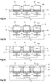
- FIGS. 1A and 1B are sectional, schematic and partial views of two examples of an optoelectronic device 1 obtained according to variants of a manufacturing process.
- the reading substrate 10 is formed of a support substrate 11 containing the reading circuit 12 of the CMOS circuit type, adapted to control and read the diodes 40.
- the reading substrate 10 has a so-called growth face, from which are the diodes 40 produced. It further comprises a plurality of conductive portions 20, distinct from each other, which define the growth face of the reading substrate 10 and are connected to the reading circuit 12.
- the read circuit 12 thus comprises active or passive electronic elements, such as diodes, transistors, capacitors, resistors, etc., electrically connected by metal interconnections to the diodes 40. It comprises a higher level of electrical interconnection comprising portions 15 of a metallic line, electrically connected to portions 13 of metallic line of a lower level of electrical interconnection by conductive vias 14. The metallic vias and lines are separated from each other by inter-metal dielectric layers 16
- the reading substrate 10 here has a flat upper face 10a at the level of which the conductive portions 15 of the metal line of the last interconnection level are exposed, as well as the inter-metal dielectric layer 16.
- the conductive vias 14 and the conductive portions 13, 15 of metal lines can be made of copper, aluminum or tungsten, by a p damascene process in which trenches made in the inter-metal dielectric layer 16 are filled with copper.
- the copper or tungsten may optionally be interposed transversely between vertical layers of titanium nitride, tantalum or the like.
- the outcrop of the conductive portions 15 at the level of the flat upper face 10a of the reading substrate 10 can be obtained by a chemical mechanical planarization technique (CMP).
- CMP chemical mechanical planarization technique
- the growth face is defined by a plurality of conductive portions 20, made of at least one electrically conductive material, for example metallic, distinct from each other, and connected to the read circuit 12.
- the conductive portions 20 are said to be distinct from each other from others, in the sense that they are physically distinct and electrically isolated from each other in the XY plane.
- Each conductive portion 20 is intended to carry a diode 40 to an electrical potential imposed by the read circuit 12, thus making it possible to inject or collect charge carriers in the diode 40.
- the conductive portions 20 may be projecting from a plane passing through a planar upper face 10a of the reading substrate 10, or flush with the planar upper face 10a. By flush, we mean "to reach the level of" or "to extend from”.
- the fig. 1A illustrates an example where the conductive portions 20 are the portions 15 of the metal line of the last interconnection level, which are flush with the flat upper face 10a of the reading substrate 10. They are separated from each other in the XY plane by the layer inter-metal dielectric 16.
- the fig. 1B illustrates another example where the conductive portions 20 are metal studs located in contact with the portions 15 of the metallic line of the last interconnection level, the latter flush with the flat upper face 10a of the reading substrate 10.
- the conductive portions 20 are studs made of at least one metallic material, for example gold, copper, aluminum, platinum, TiN, among others. They are distinct from each other in the XY plane. They have dimensions in the XY plane which depend on the desired lateral dimensions of the diodes 40.
- the lateral dimensions can be between 500 nm and a few millimeters, depending on the intended applications of the diodes 40, and preferably between 1 ⁇ m and 10 ⁇ m. They have a thickness, along the Z axis, for example between 50 nm and 1 ⁇ m.
- the optoelectronic device 1 comprises a plurality of nucleation portions 30, allowing nucleation and epitaxial growth of the diodes 40. They are distinct from each other, in the sense that they are physically distinct and electrically isolated from each other in the plane XY. They are arranged in contact with the conductive portions 20, and can thus participate in injecting the charge carriers into the diodes 40 or in collecting the photogenerated charge carriers. They have lateral dimensions in the XY plane, preferably substantially equal to or even less than those of the conductive portions 20.
- the nucleation portions 30 are made of one or more monolayers of a two-dimensional crystalline material.
- This two-dimensional material is chosen as a function of the semiconductor material of interest of the diodes 40.
- the two-dimensional material is preferably chosen from graphene or a dichalcogenide of a metal of transition, such as MoS 2 , MoSe 2 , WSe 2 , MoTe 2 , WTe 2 , ZrS 2 , TiS 2 , among others.
- the two-dimensional material is a III-V type alloy
- the two-dimensional material is preferably chosen from graphene, a dichalcogenide of a transition metal, or even a monochalcogenide in particular based on Ga, Te or Se, by example of GaSe, GaTe or InSe, in particular when the semiconductor material of interest is respectively based on Ga, Te or Se.
- the nucleation portions 30 are made of molybdenum or tungsten sulfide, and the conductive layers 20 are made of gold. This gives higher adhesion.
- the optoelectronic device 1 comprises a matrix of diodes 40, which each have a pn or pin type semiconductor junction, or even a so-called "barrier" diode junction (for example pBn or nBn).
- the diodes 40 are photodiodes or light-emitting diodes. They can be adapted to detect or emit electromagnetic radiation of interest, for example in the infrared or visible.
- the diodes 40 comprise an n-doped semiconductor part and a p-doped semiconductor part, between which an intrinsic part (not intentionally doped) may be present.
- the diodes 40 may have a conventional structure which is not described in more detail here.
- the semiconductor junction can be formed by two doped semiconductor parts stacked one on the other, optionally separated from each other by an active area possibly comprising quantum wells. It can also be formed by a locally doped well located on the surface of a semiconductor part.
- the diodes 40 are made based on the semiconductor material of interest, for example based on CdTe, InGaAs, antimony Sb, GaN, Si and / or Ge etc. They each have a lower face situated in contact with the nucleation portions 30, an upper face 40a opposite along the axis Z and forming an optical transmission or reception face, as well as a lateral face 40b which connects the lower faces and higher between them and delimits the diode transversely in the XY plane.
- the diodes 40 can have different shapes in the XY plane, for example a polygonal shape, for example square, rectangular, triangular, hexagonal, or even a circular or oval shape.
- the diameter of the diodes 40 is here a quantity associated with its perimeter at the level of a section in the XY plane.
- the diameter of each diode 40 can be constant along the Z axis, or even can vary along the + Z direction.
- the dimensions are preferably identical, from one diode to another.
- the lateral dimensions, in the XY plane can be between 500 nm and a few millimeters, depending on the intended applications, and preferably between 1 ⁇ m and 10 ⁇ m.
- the optoelectronic device 1 comprises an intermediate insulating layer 50, which extends in contact with each diode 40 in the XY plane and fills the inter-diode spacing.
- This layer 50 preferably extends entirely along the lateral faces 40b of the diodes 40 along the axis Z, here starting from the growth face of the reading substrate 10. It advantageously ensures the passivation of the lateral sides of the diodes 40, thus making it possible to reduce the surface component of the dark current (photodiodes) or to limit the effect of any surface states which may lead to non-radiative recombinations (emitting diodes). This improves the optical and / or electronic properties of the diodes 40.
- the intermediate insulating layer 50 is made of at least one electrically insulating material, for example dielectric, which can depend on the semiconductor material of interest of the diodes 40. It provides insulation the diodes 40 between them in the XY plane. It can be formed from the same electrically insulating material, or can be formed from different layers of different materials, for example from a passivation sublayer 51 covered with a filling layer 52.
- the fig. 1A illustrates an example where the insulating intermediate layer 50 is formed of a passivation sublayer 51 which is in contact with and covers the lateral face 40b of the diodes 40, and of a filling layer 52 which covers the passivation sublayer 51 and fills the inter-diode spacing in the XY plane.
- the intermediate insulating layer 50 extends from the reading substrate 10 along the Z axis: it therefore provides physical and electrical isolation of both the nucleation portions 30 from one another, and diodes 40 between them on the other hand.
- the intermediate insulating layer 50 can be made of different materials (passivation and filling).
- the passivation sublayer 51 can be made from CdTe
- the filler layer 52 can be made from ZnS, SiO, or SiN, among others.
- the fig. 1B illustrates another example where the intermediate insulating layer 50 comprises a lower insulating part 53 and an upper insulating part stacked one on the other along the axis Z. More specifically, the lower insulating part 53 here extends in contact and from the growth face along the Z axis, and extends between and in contact with the conductive portions 20 and the nucleation portions 30. It may in particular correspond to a growth mask used during the epitaxy of the diodes 40 It has a thickness at least equal to the thickness of the conductive portions 20 and of the nucleation portions 30.
- the lower insulating part 53 can be made of at least one dielectric material, for example a silicon oxide SiO or a silicon nitride. SiN, among others.
- the upper insulating part extends along the axis Z starting from the lower insulating part 53, and extends in the XY plane between and in contact with the diodes 40. It is here formed of a passivation sublayer 51 located in contact with the lateral faces, and with a filling layer 52.
- the passivation sublayer 51 may be an oxide of the III-V semiconductor material, obtained for example by electrochemical oxidation of the III-V semiconductor material
- the filler layer 52 may be a silicon oxide or nitride, which covers the passivation sublayer 51 and fills the spacing between the diodes 40 in the XY plane.
- the optoelectronic device 1 comprises an upper bias electrode, here in the form of an upper conductive layer 60 extending in contact with the upper face 40a of each diode 40, and connected to the reading circuit 12.
- the upper conductive layer 60 is made of at least one electrically conductive material. It can thus be ITO, possibly doped ZnO, perovskites such as SrTiO 3 and Cd 3 TeO 6 , doped CdO, possibly doped In 2 O 3 , TiO 2 , VO 2 , among others. It can extend so as to continuously cover the upper faces 40a of the diodes 40 ( fig. 1A ) and is therefore made of at least one conductive material transparent to the electromagnetic radiation of interest.
- the transmission coefficient is greater than or equal to 50% for a central wavelength of the electromagnetic radiation of interest. It can also extend partially on the upper faces 40a of the diodes 40 (fig.lB), in particular on the edge thereof, so as to reduce any optical absorption.
- the electrode forms a connected contact grid (seen from above) and we could favor an electrode made of metal insofar as it will not obstruct light entering or leaving through the upper faces of the diodes.
- an insulating transparent layer 61 can cover the diodes 40 and the upper conductive layer 60. This insulating transparent layer 61 can have a surface structuring in particular to improve the extraction and / or the optical focusing, among others. Other variations are possible.
- the upper conductive layer 60 can be a continuous thin layer at least partially transparent, on which extends a metal grid located opposite the intermediate insulating layer 50, this grid thus making it possible to better recover / extract the charge carriers and to compensate for the possible high electrical resistivity of the thin layer 60.
- the thin layer 60 can be produced, in addition to the materials indicated above, in doped amorphous silicon, which makes it possible to improve the passivation of the upper face of the diodes.
- the optoelectronic device 1 comprises a matrix of diodes 40 obtained from a reading substrate 10 by means of nucleation portions 30 of a two-dimensional crystalline material, which are in electrical contact with portions conductors 20 connected to the reading circuit 12.
- the diodes 40 are produced by van der Waals epitaxy from the two-dimensional material of the nucleation portions 30. They therefore have a crystal lattice which is not mechanically constrained by that of the nucleation portions 30 , nor by the reading substrate 10.
- the effective lattice parameter of the semiconductor material of the diodes 40, in particular that of the lower parts in contact with the nucleation portions 30 is substantially equal to its value in the natural state (unconstrained ).
- the diodes 40 are pixelated from the epitaxial growth from the nucleation portions 30 distinct from each other. This reduces the risk of degradation of the crystalline quality of the semiconductor material of the diodes 40, in particular at the side flanks, since the pixelation of the diodes 40 is not carried out by a growth step of a semiconductor stack followed by a localized etching step to pixelate the diodes 40. The optical and / or electronic properties of the optoelectronic device 1 are thus improved.
- the diodes 40 are produced from the reading substrate 10 by means of the nucleation portions 30 of two-dimensional material formed in contact with the conductive portions 20. This thus avoids the hybridization steps, that is that is to say mechanical assembly by transfer and electrical connection, from an optoelectronic chip to a control chip. This avoids the risks of misalignment and / or loss of mechanical and therefore electrical contact between the interconnection pads of the control chip and the diodes 40 of the optoelectronic chip. It is then possible that the optoelectronic device 1 comprises a matrix of diodes 40 comprises a large number of diodes 40 at low pitch. In addition, the composition of the material forming neighboring diodes can be different from one diode to another, allowing the creation of a multi-spectral device.
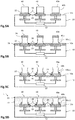
- FIGS. 2A to 2G are schematic and partial views, in section, of different steps of a process for manufacturing an optoelectronic device 1 to array of photodiodes 40, according to a variant of the embodiment illustrated in the fig. 1A .
- a reading substrate 10 is produced, formed of a support substrate 11 containing a CMOS type reading circuit 12.
- the read circuit 12 comprises different portions 13, 15 of metallic line, separated from each other in the XY plane by an inter-metal dielectric layer 16, here made of a silicon oxide.
- the portions 13, 15 of the different interconnection levels are connected together by conductive vias 14, and are thus connected to the reading circuit 12. Portions 15 of the metal line of the last interconnection level are flush with the flat upper face 10a of the reading substrate 10.
- the conductive portions 20 are produced by conventional deposition, photolithography and localized etching steps. In this example, these project from the planar upper face 10a of the reading substrate 10, and are arranged in contact with the portions 15 of the metal line of the last interconnection level.
- the upper face of the conductive portions 20 participates in defining the growth face of the reading substrate 10. In this example, they have lateral dimensions substantially equal to those of the portions of the metal line, but they can have different dimensions.
- the conductive portions 20 are here preferably made of gold. Here they have a thickness of the order of 500 nm and lateral dimensions of the order of 10 ⁇ m. They are thus distinct from each other in the XY plane and are adapted to polarize the diodes 40.
- the nucleation portions 30 are produced on and in contact with the conductive portions 20.
- a first mask 71 formed here of a photosensitive resin.
- This mask 71 extends over the surface left free of the flat upper face 10a of the reading substrate 10, that is to say between the conductive portions 20.
- This mask 71 preferably has a thickness greater than that of the conductive portions 20 and nucleation portions 30, for example of the order of 1 ⁇ m.
- the nucleation portions 30 are made of a two-dimensional crystalline material.
- the two-dimensional crystalline material is advantageously a sulfur material, and can be MoS 2 because of the high affinity between gold and sulfur, thus making it possible to reduce the risks of delamination.
- the two-dimensional crystalline material is here electrically conductive, so as to allow the polarization of the diodes 40. It may have a small number of atomic monolayers, for example be formed of a single monolayer, so as to promote the transmission of electric current in particular by tunnel effect.
- the nucleation portions 30 can be carried out by molecular beam epitaxy (MBE, for Molecular Beam Epitaxy, in English), by chemical vapor deposition (CVD, for Chemical Vapor Deposition, in English) such as chemical vapor deposition organometallic (MOCVD) or atomic layer deposition (ALD, for Atomic Layer Deposition , among others).
- MBE molecular beam epitaxy
- CVD chemical vapor deposition
- MOCVD chemical vapor deposition organometallic
- ALD atomic layer deposition
- the temperature at which the nucleation portions 30 are produced is preferably less than or equal to 400 ° C., so as to avoid any degradation of the reading circuit 12.
- the two-dimensional crystalline material is here deposited both on the upper face of the conductive portions 20 and on the upper face of the first mask.
- the first mask is then removed, for example by lift-off.
- the nucleation portions 30 can be formed by transfer or transfer of a continuous layer of a two-dimensional crystalline material, in particular when the growth face is planar and coincides with the planar upper face 10a of the reading substrate 10, otherwise said when the conductive portions 20 are not projecting with respect to the planar upper face 10a but are flush with the latter.
- the continuous layer of the two-dimensional crystalline material may be a continuous layer of graphene formed by graphitization of a SiC substrate with a hexagonal crystal lattice by annealing at high temperature under vacuum, followed by transfer of the continuous layer of graphene to the face. upper plane 10a of the reading substrate 10.
- a localized etching step of the continuous graphene layer is then implemented so as to obtain the nucleation portions 30, distinct from each other, and located on and in contact with the conductive portions 20.
- the article of Avouris and Dimitrakopoulos entitled Graphene synthesis and applications, Materialstoday, 03/2012, Vol. 15, n ° 3 , details of the conventional techniques making it possible to produce a continuous layer of graphene, in particular the graphitization of the SiC substrate followed by the transfer.
- the diodes 40 are produced by van der Waals epitaxy from the nucleation portions 30.
- a second mask 72 is produced beforehand, here a growth mask, situated on the surface left free of the planar upper face 10a of the reading substrate 10, that is to say between the conductive portions 20 and the nucleation portions 30.
- the growth mask 72 here has a thickness along the axis Z greater than or equal to the final thickness of the diodes 40, but as a variant may have a thickness less than this. It can be made of a dielectric material, for example a silicon oxide SiO or a silicon nitride SiN, among others.
- the diodes 40 are then produced by epitaxial growth from the nucleation portions 30 of a semiconductor material of interest of type II-VI, of type III-V, or even of type IV.
- This epitaxy growth step may include a nucleation phase followed by a growth phase proper, these two phases being distinguished from each other by the growth conditions and in particular by the value of the growth temperature.
- the epitaxial growth step can comprise a single nucleation and growth phase.
- CVD chemical vapor deposition
- MOCVD organometallic
- MBE molecular beam epitaxy
- HVPE hydride vapor epitaxy
- ALE atomic layer epitaxy
- ALD atomic layer deposition
- the diodes 40 are produced by MBE epitaxy at a growth temperature of the order of approximately 400 ° C., so as to avoid any degradation of the reading circuit 12.
- the semiconductor material of the diodes 40 is linked to the nucleation portions 30 by weak bonds of the van der Waals type, and not by covalent or ionic bonds.
- the semiconductor material can thus nucleate at its substantially natural lattice parameter, and is therefore not substantially constrained by a possible lattice mismatch between the nucleation portions 30 and the semiconductor material.
- the intermediate insulating layer 50 is produced.
- the growth mask 72 is first of all removed, for example by selective chemical means. In this example, it is deleted all over thickness, but as a variant, and as detailed below, a lower part of the growth mask situated in contact with the reading substrate 10 can be kept.
- the intermediate insulating layer 50 is then deposited, made of at least one electrically insulating material, so as to come into contact with the side faces 40b of the diodes 40 along the entire thickness of the latter, and to fill the space between the diodes 40
- the insulating intermediate layer 50 can thus be formed of a passivation sublayer of CdTe which extends in contact with the lateral face 40b of the diodes 40, coated with a filling layer of ZnS, SiO, SiN, among others, which covers the passivation sublayer and fills the inter-diode spacing.
- the passivation sublayer can also be produced by oxidation of the semiconductor material of the diodes 40.
- the insulating intermediate layer 50 can be produced in a same material, for example in a silicon oxide, a silicon nitride, a silicon oxynitride, or in Al 2 O 3 , among others.
- the intermediate insulating layer 50 opens out substantially at the level of the upper face 40a of the diodes 40. In this example, it covers part of the lateral edge of the upper face 40a.
- the upper conductive layer 60 is produced, so as to come into contact with the upper face 40a of the diodes 40.
- the upper conductive layer 60 completely covers the upper face 40a of the diodes 40. It is therefore made of a material , not only electrically conductive, but also transparent to the electromagnetic radiation of interest. The choice of material depends in particular on the central wavelength of the spectral range of detection or emission of the diodes 40.
- the upper conductive layer 60 can be produced by CVD deposition, for example by ALD deposition, by spray assisted by ion beams (IBS, for Ion Beam Sputtering, in English), or even by sol-gel deposition, among others.
- the upper conductive layer 60 is connected to the read circuit 12 of the read substrate 10.
- the manufacturing process makes it possible to produce a matrix of diodes 40 from a reading substrate 10, by van der Waals type epitaxy from a plurality of nucleation portions 30 made of a two-dimensional crystalline material, those -this being located in contact with conductive portions 20 connected to the reading circuit 12.
- the crystalline quality of the semiconductor material of the diodes 40 is improved by the fact that it is no longer constrained by the mesh parameter of the nucleation material, due to the fact that an epitaxy of the van der Waals type is implemented.
- the manufacturing process also ensures pixelation of the diodes 40 from the epitaxial growth, and does not require localized etching of a semiconductor stack of continuous crystalline layers to form the diodes 40, as is the case in particular in the case of the processes. loophole type manufacturing. The manufacturing process thus makes it possible to produce a matrix of diodes 40 with high crystalline quality comprising a large number of diodes 40 with low pitch.
- FIGS. 3A to 3D are schematic and partial views, in section, of different steps of a method of manufacturing an optoelectronic device 1 with a diode array 40 according to the embodiment illustrated in the fig. 1B .
- the steps for producing the reading substrate 10, conductive portions 20 and nucleation portions 30 are identical or similar to those described with reference to fig. 2A to 2D , and are not included here.
- the diodes 40 are produced by van der Waals epitaxy from the nucleation portions 30 of a two-dimensional crystalline material.
- a growth mask 72 is produced beforehand situated on the surface left free of the growth face of the reading substrate 10, that is to say between the conductive portions 20 and the nucleation portions 30.
- the mask 72 growth here has a thickness along the axis Z less than the final thickness of the diodes 40, but greater than or equal to the thickness of the conductive portion 20 and the nucleation portion 30.
- the growth mask 72 makes it possible to guarantee that the positioning in the XY plane of each nucleation portion 30 vis-à-vis the underlying conductive portion 20 is maintained.
- the growth mask 72 may have a thickness of the order of 500 nm. It can be made of a dielectric material, for example a silicon oxide SiO or a silicon nitride SiN, among others.
- a passivation sub-layer 51 of the insulating intermediate layer 50 is then produced.
- a mask 73 is first deposited locally, here a photosensitive resin, so as to cover only the upper face 40a of the diodes 40.
- the side face 40b of the diodes 40 is left free, that is to say not covered.
- Electrochemical oxidation is then carried out, so as to form a passivation sublayer 51 produced from an oxide of the semiconductor material of the diodes 40.
- This sublayer 51 thus covers the lateral face 40b of the corresponding diode 40, preferably continuously.
- the intermediate insulating layer 50 we then finalize the production of the intermediate insulating layer 50.
- the filling layer 52 is substantially flush with the upper face of the diodes 40. It covers here a lateral border of the upper face 40a of the diodes 40.
- the upper conductive layer 60 is then produced, so that it comes into contact with the upper face 40a of each diode.
- the upper conductive layer 60 does not entirely cover the upper faces 40a but only covers a lateral border of the latter and forms an electrode of preferentially connected nature (contact remaining common to all the diodes). This limits the possible partial absorption of the electromagnetic radiation of interest by the upper conductive layer 60.
- a protective layer 61 made of an electrically insulating and transparent material to the electromagnetic radiation of interest is then deposited so as to continuously cover the diodes 40 as well as the upper conductive layer 60. It can have a surface structure having a defined optical function (light extraction, shaping of the light beam emitted or received ...)
- An optoelectronic device 1 is thus obtained with diode arrays 40 produced from a reading substrate 10 and having a good crystalline quality, by means of nucleation portions 30 of a two-dimensional crystalline material arranged in contact with conductive portions 20 of the substrate. reading 10.
- FIGS. 4A to 4D are schematic and partial views, in section and in top view along the plane AA, of different stages of a method of manufacturing an optoelectronic device 1 according to an alternative embodiment.
- the manufacturing process is similar to those described above, and differs in particular in that it makes it possible to improve the electrical conduction between the conductive portions 20 and the nucleation portions 30.
- a conductive portion 20 is produced for each diode 40 which comprises a main zone 21 intended to be coated by the epitaxial diode, and a lateral zone 22 which extends in the XY plane from the zone main 21.
- the lateral zone 22 has dimensions in the XY plane, preferably less than those of the main zone 21, and is intended to improve the electrical contact with the nucleation portion 30.
- the nucleation portion 30 is produced, as described above, so that it is located on and in contact with the conductive portion 20, both on the main 21 and lateral 22 areas of the latter. It thus comprises a lateral part 32, situated on and in contact with the lateral zone 22, which extends laterally from a main part 31.
- the lateral part 32 does not entirely cover the lateral zone 22, so that a side face of the nucleation portion 30 is located there. More precisely, each main zone 21 of the conductive portion 20 is coated by the nucleation portion 30, but the lateral zone 22 is only partially coated by the nucleation portion 30.
- Each lateral part 32 of the nucleation portion 30 has thus a lateral face 32.3 situated above the lateral zone 22 of the conductive portion 20, which connects a lower face 32.1 of the nucleation portion 30 in contact with the conductive portion 20 and an opposite upper face 32.2.
- an upper lateral part 23 of the conductive portion 20 comes into contact with the wafer, that is to say of the lateral face 32.3 of the part lateral 32 of the nucleation portion 30, and advantageously covers the lateral part 32.
- This upper lateral part 23 of the conductive portion extends continuously in contact with the lateral zone 22 and the lateral face of the nucleation portion 30, and leaves the main zone 21 free.
- the upper lateral part 23 extends in contact with the conductive portion 20 underlying, and in contact with the lateral face 32.3 of the nucleation portion 30, and advantageously in contact with the upper face 32.2. It can thus be considered that the nucleation layer 20 is formed by a lower part (indicated by the reference 20 in the figures) and by the upper lateral part 23.
- the production of the optoelectronic device 1 is finalized as described above, by the steps of van der Waals epitaxy of the diodes 40 from the main part 31 of the nucleation portions 30, production of the insulating intermediate layer 50, and production of the upper conductive layer 60. These steps are identical or similar to those described above and are not repeated here.
- the van der Waals epitaxy step can be carried out before the step for producing the upper lateral parts 23.
- the diodes 40 cover the main zone 21 but do not cover the lateral zone 22.
- the upper lateral part 23 is advantageously in contact with a lower surface 40b.1 of a side face of the diode 40.
- an optoelectronic device 1 is thus obtained, the electrical contact between the conductive portions 20 and the nucleation portions 30 is improved. Indeed, it appears that the electrical contact in the plane, between the conductive portions 20 and the nucleation portions 30, can be resistive depending on the materials used. However, it appears that the electrical contact can be less resistive when it takes place in particular at the level of the edge of the nucleation portions 30, that is to say by the lateral face which connects the lower and upper faces of the portions of nucleation 30.
- the upper lateral part 23 of the conductive portions 20 in fact comprises an area which comes into contact with the edge of the nucleation portions 30, thereby improving the electrical conduction between the conductive portion and the nucleation portion. The performance of the optoelectronic device 1 is then preserved, or even improved.
- FIGS. 5A to 5D are schematic and partial views, in section, of different stages of a method of manufacturing an optoelectronic device 1 according to another alternative embodiment.
- the manufacturing process is similar to those described above, and differs in particular in that it makes it possible to improve the electrical conduction between the conductive portions 20 and the diodes 40. Certain steps are identical or similar to those described above and are not repeated here.
- a matrix of diodes 40 is first produced by van der Waals epitaxy from the nucleation portions 30. It will be ensured that the diode junctions are preferably positioned near or at the level of the top part of the portions 40.
- the conductive portions 20 each comprise a lateral zone 22 of which an upper surface is free, that is to say not coated by the nucleation portion 30 and by the diodes 40.
- the lateral zone 22 here extends over the entire contour diodes 40, but may be present only on part of the contour.
- Each nucleation portion 30 thus has a lateral face 32.3 situated above the lateral zone 22 of the conductive portion 20, which connects a lower face 32.1 of the nucleation portion 30 in contact with the conductive portion 20 and an upper face 32.2 opposite.
- an isotropic selective etching of the diodes 40 is carried out at their lateral face 40b, so that the lateral faces 40b have an inclined lower surface 40b.1.
- a photosensitive resin is deposited so as to cover the upper face 40a of the diodes 40 as well as the conductive portions 20, the nucleation portions 30 and the reading substrate 10.
- the selective etching is carried out by an etching agent reactive to the semiconductor material of the diodes 40.
- the lateral face 40b of the diodes then has a narrowing of its diameter in a median zone of the diodes 40 along the axis Z. Also, it has a surface lower inclined 40b.1, in other words concave, which extends from the nucleation portion 30 along the axis Z.
- an upper lateral part 23 of the conductive portions 20 which extends continuously in contact with the lateral zone 22 of the conductive portion and the inclined lower surface 40b is produced. 1.
- the diodes 40 and the reading substrate 10 are coated with a photosensitive resin (not shown), which is etched locally only at the level of the inclined lower surfaces 40b.1 and at the level of the free upper surface of the lateral zone 22 of the conductive portions 20.
- the edge of the nucleation portions 30 is also made free.
- a conductive material is then deposited, preferably identical to that of the conductive portions 20, for example in gold, so as to form an upper lateral part 23 continuously covering, for each diode, the free upper surface of the lateral zone 22 of the conductive portion and the inclined lower surface 40b.1 of the diode.
- the edge of the nucleation portion 30 is also covered by the upper side portion 23.
- the photosensitive resin and the gold layer which covers it are then removed by lift-off .
- the upper lateral part 23 extends in contact with the underlying conductive portion 20 and in contact with the lower surface 40b. 1 of the diode 40, as well as, here, in contact with the lateral face 32.3 of the nucleation portion 30.
- the realization of the optoelectronic device 1 is finalized as described above, by the steps for producing the insulating intermediate layer 50 and for making the upper conductive layer 60. These steps are identical or similar to those described above and are not repeated here .
- An optoelectronic device 1 is thus obtained, the electrical conduction between the conductive portions 20 and the diodes 40 is improved. Indeed, it appears that the electrical contact in the plane between the nucleation portions 30 and the semiconductor material of the diodes 40 can be resistive depending on the materials used. Also, the upper lateral part 23 of the conductive portions 20 makes it possible to improve the electrical conduction with the diodes 40, by forming an additional area of electrical conduction at the edge of the nucleation portions 30. The performances of the optoelectronic device 1 are then preserved, improved.
- peripheral lateral portion of the conductive portions 20 described with reference to the 4D figures and 5D may extend over the entire border of the diodes 40 in the XY plane, or may only extend over part of the border.
- the diodes 40 may be identical to each other, particularly in the case of monospectral emission or detection. As a variant, they can differ from one another by the composition of the semiconductor material, in particular in the case of multispectral use of the optoelectronic device 1. In this case, several successive epitaxy steps are applied, taking care to mask, each time , areas that are not intended to accommodate the material being deposited.
Landscapes
- Engineering & Computer Science (AREA)
- Power Engineering (AREA)
- Computer Hardware Design (AREA)
- Microelectronics & Electronic Packaging (AREA)
- Physics & Mathematics (AREA)
- Condensed Matter Physics & Semiconductors (AREA)
- General Physics & Mathematics (AREA)
- Electromagnetism (AREA)
- Manufacturing & Machinery (AREA)
- Chemical & Material Sciences (AREA)
- Inorganic Chemistry (AREA)
- Light Receiving Elements (AREA)
- Solid State Image Pick-Up Elements (AREA)
- Led Devices (AREA)
Applications Claiming Priority (1)
| Application Number | Priority Date | Filing Date | Title |
|---|---|---|---|
| FR1873790A FR3091026B1 (fr) | 2018-12-21 | 2018-12-21 | procede de fabrication d’une pluralité de diodes à partir d’un substrat de lecture |
Publications (1)
| Publication Number | Publication Date |
|---|---|
| EP3671843A1 true EP3671843A1 (de) | 2020-06-24 |
Family
ID=66867285
Family Applications (1)
| Application Number | Title | Priority Date | Filing Date |
|---|---|---|---|
| EP19217669.1A Withdrawn EP3671843A1 (de) | 2018-12-21 | 2019-12-18 | Herstellungsverfahren einer vielzahl von dioden aus einem lesesubstrat |
Country Status (3)
| Country | Link |
|---|---|
| US (1) | US20200203400A1 (de) |
| EP (1) | EP3671843A1 (de) |
| FR (1) | FR3091026B1 (de) |
Citations (2)
| Publication number | Priority date | Publication date | Assignee | Title |
|---|---|---|---|---|
| WO2015044619A1 (fr) | 2013-09-30 | 2015-04-02 | Aledia | Dispositif optoélectronique a diodes électroluminescentes |
| FR3023066A1 (fr) * | 2014-06-30 | 2016-01-01 | Aledia | Dispositif optoelectronique comprenant des diodes electroluminescentes et un circuit de commande |
Family Cites Families (2)
| Publication number | Priority date | Publication date | Assignee | Title |
|---|---|---|---|---|
| DE102004025684A1 (de) * | 2004-04-29 | 2005-11-17 | Osram Opto Semiconductors Gmbh | Optoelektronischer Halbleiterchip und Verfahren zum Ausbilden einer Kontaktstruktur zur elektrischen Kontaktierung eines optoelektronischen Halbleiterchips |
| FR3005788B1 (fr) * | 2013-05-14 | 2016-10-21 | Commissariat Energie Atomique | Dispositif optoelectronique et son procede de fabrication |
-
2018
- 2018-12-21 FR FR1873790A patent/FR3091026B1/fr not_active Expired - Fee Related
-
2019
- 2019-12-18 EP EP19217669.1A patent/EP3671843A1/de not_active Withdrawn
- 2019-12-20 US US16/722,266 patent/US20200203400A1/en not_active Abandoned
Patent Citations (2)
| Publication number | Priority date | Publication date | Assignee | Title |
|---|---|---|---|---|
| WO2015044619A1 (fr) | 2013-09-30 | 2015-04-02 | Aledia | Dispositif optoélectronique a diodes électroluminescentes |
| FR3023066A1 (fr) * | 2014-06-30 | 2016-01-01 | Aledia | Dispositif optoelectronique comprenant des diodes electroluminescentes et un circuit de commande |
Non-Patent Citations (1)
| Title |
|---|
| A. ROGALSKI: "Progress in Quantum Electronics", PROGRESS IN FOCAL PLANE ARRAY TECHNOLOGIES, vol. 36, 2012, pages 342 - 473 |
Also Published As
| Publication number | Publication date |
|---|---|
| FR3091026B1 (fr) | 2020-12-11 |
| US20200203400A1 (en) | 2020-06-25 |
| FR3091026A1 (fr) | 2020-06-26 |
Similar Documents
| Publication | Publication Date | Title |
|---|---|---|
| EP3667728B1 (de) | Verfahren zur herstellung einer vorrichtung mit lichtemittierenden und/oder lichtempfangenden dioden und mit einem selbst ausgerichteten kollimationsgitter | |
| EP0350351B1 (de) | Fotodiode und Fotodiodenmatrix aus II-VI-Halbleitermaterial und Herstellungsverfahren dafür | |
| EP3657556B1 (de) | Herstellungsverfahren mindestens einer passivierten planaren fotodiode mit reduziertem dunkelstrom | |
| EP3660930B1 (de) | Herstellungsverfahren einer fotodiodenmatrix auf germaniumbasis und mit schwachem dunkelstrom | |
| EP3479409B1 (de) | Optoelektronische vorrichtung mit dreidimensionalen dioden | |
| FR2923651A1 (fr) | Procede de realisation d'une jonction pn dans un nanofil, et d'un nanofil avec au moins une jonction pn. | |
| FR3080487A1 (fr) | Procede de fabrication d’un dispositif optoelectronique a matrice de diodes | |
| EP3971995A1 (de) | Passivierte fotodiode mit einem ferroelektrischen peripheren teil | |
| EP3347917A1 (de) | Leuchtemittierende vorrichtung mit integriertem lichtsensor | |
| FR3075468A1 (fr) | Procede de fabrication d'un dispositif optoelectronique par report d'une structure de conversion sur une structure d'emission | |
| EP3109900B1 (de) | Herstellungsverfahren einer vielzahl von dipolen in form von inseln, die selbstausrichtende elektroden umfassen | |
| WO2010061151A2 (fr) | Procede de fabrication de cellules matricielles photosensibles dans l'infrarouge collees par adhesion moleculaire sur substrat optiquement transparent et capteur associe | |
| EP3396720B1 (de) | Herstellungsverfahren einer fotodiodenmatrix mit mesa-strukturen | |
| EP3732725B1 (de) | Optoelektronische vorrichtung mit einer matrix aus dreidimensionalen dioden | |
| EP3671843A1 (de) | Herstellungsverfahren einer vielzahl von dioden aus einem lesesubstrat | |
| FR3060852A1 (fr) | Dispositif photovoltaique et procede de fabrication associe | |
| EP3563426B1 (de) | Verfahren zur herstellung einer optoelektronischen vorrichtung mit einem schritt zum ätzen der rückseite des wachstumssubstrats | |
| EP4184594B1 (de) | Germanium-photodiode mit reduziertem dunkelstrom mit einem auf sige/ge basierenden peripheren zwischenteil | |
| WO2019025354A1 (fr) | Procede de fabrication ameliore d'un detecteur optique a base de photodiodes et dispositif associe | |
| EP4292136A1 (de) | Germanium-photodiode mit optimierten metallkontakten | |
| FR2932013A1 (fr) | Procede de fabrication d'une cellule photovoltaique a nanofils | |
| WO2022069506A1 (fr) | Dispositif optoelectronique | |
| WO2023006846A1 (fr) | Procede de fabrication d'un dispositif optoelectronique comportant une etape de realisation d'une couche mince conductrice de maniere conforme et continue par depot directif | |
| EP4092746A1 (de) | Verfahren zur herstellung einer optoelektronischen vorrichtung | |
| FR3105878A1 (fr) | Dispositif à composants optoélectroniques tridimensionnels pour découpe au laser et procédé de découpe au laser d'un tel dispositif |
Legal Events
| Date | Code | Title | Description |
|---|---|---|---|
| PUAI | Public reference made under article 153(3) epc to a published international application that has entered the european phase |
Free format text: ORIGINAL CODE: 0009012 |
|
| STAA | Information on the status of an ep patent application or granted ep patent |
Free format text: STATUS: REQUEST FOR EXAMINATION WAS MADE |
|
| 17P | Request for examination filed |
Effective date: 20191218 |
|
| AK | Designated contracting states |
Kind code of ref document: A1 Designated state(s): AL AT BE BG CH CY CZ DE DK EE ES FI FR GB GR HR HU IE IS IT LI LT LU LV MC MK MT NL NO PL PT RO RS SE SI SK SM TR |
|
| AX | Request for extension of the european patent |
Extension state: BA ME |
|
| 18W | Application withdrawn |
Effective date: 20210331 |