EP4292136B1 - Photodiode germanium a contacts metalliques optimises - Google Patents
Photodiode germanium a contacts metalliques optimises Download PDFInfo
- Publication number
- EP4292136B1 EP4292136B1 EP22704381.7A EP22704381A EP4292136B1 EP 4292136 B1 EP4292136 B1 EP 4292136B1 EP 22704381 A EP22704381 A EP 22704381A EP 4292136 B1 EP4292136 B1 EP 4292136B1
- Authority
- EP
- European Patent Office
- Prior art keywords
- semiconductor portion
- region
- photodiode
- contact
- semiconductor
- Prior art date
- Legal status (The legal status is an assumption and is not a legal conclusion. Google has not performed a legal analysis and makes no representation as to the accuracy of the status listed.)
- Active
Links
Images


Classifications
-
- H—ELECTRICITY
- H10—SEMICONDUCTOR DEVICES; ELECTRIC SOLID-STATE DEVICES NOT OTHERWISE PROVIDED FOR
- H10F—INORGANIC SEMICONDUCTOR DEVICES SENSITIVE TO INFRARED RADIATION, LIGHT, ELECTROMAGNETIC RADIATION OF SHORTER WAVELENGTH OR CORPUSCULAR RADIATION
- H10F77/00—Constructional details of devices covered by this subclass
- H10F77/20—Electrodes
- H10F77/206—Electrodes for devices having potential barriers
-
- H—ELECTRICITY
- H10—SEMICONDUCTOR DEVICES; ELECTRIC SOLID-STATE DEVICES NOT OTHERWISE PROVIDED FOR
- H10F—INORGANIC SEMICONDUCTOR DEVICES SENSITIVE TO INFRARED RADIATION, LIGHT, ELECTROMAGNETIC RADIATION OF SHORTER WAVELENGTH OR CORPUSCULAR RADIATION
- H10F30/00—Individual radiation-sensitive semiconductor devices in which radiation controls the flow of current through the devices, e.g. photodetectors
- H10F30/20—Individual radiation-sensitive semiconductor devices in which radiation controls the flow of current through the devices, e.g. photodetectors the devices having potential barriers, e.g. phototransistors
- H10F30/21—Individual radiation-sensitive semiconductor devices in which radiation controls the flow of current through the devices, e.g. photodetectors the devices having potential barriers, e.g. phototransistors the devices being sensitive to infrared, visible or ultraviolet radiation
- H10F30/22—Individual radiation-sensitive semiconductor devices in which radiation controls the flow of current through the devices, e.g. photodetectors the devices having potential barriers, e.g. phototransistors the devices being sensitive to infrared, visible or ultraviolet radiation the devices having only one potential barrier, e.g. photodiodes
- H10F30/221—Individual radiation-sensitive semiconductor devices in which radiation controls the flow of current through the devices, e.g. photodetectors the devices having potential barriers, e.g. phototransistors the devices being sensitive to infrared, visible or ultraviolet radiation the devices having only one potential barrier, e.g. photodiodes the potential barrier being a PN homojunction
-
- H—ELECTRICITY
- H10—SEMICONDUCTOR DEVICES; ELECTRIC SOLID-STATE DEVICES NOT OTHERWISE PROVIDED FOR
- H10F—INORGANIC SEMICONDUCTOR DEVICES SENSITIVE TO INFRARED RADIATION, LIGHT, ELECTROMAGNETIC RADIATION OF SHORTER WAVELENGTH OR CORPUSCULAR RADIATION
- H10F30/00—Individual radiation-sensitive semiconductor devices in which radiation controls the flow of current through the devices, e.g. photodetectors
- H10F30/20—Individual radiation-sensitive semiconductor devices in which radiation controls the flow of current through the devices, e.g. photodetectors the devices having potential barriers, e.g. phototransistors
- H10F30/21—Individual radiation-sensitive semiconductor devices in which radiation controls the flow of current through the devices, e.g. photodetectors the devices having potential barriers, e.g. phototransistors the devices being sensitive to infrared, visible or ultraviolet radiation
- H10F30/22—Individual radiation-sensitive semiconductor devices in which radiation controls the flow of current through the devices, e.g. photodetectors the devices having potential barriers, e.g. phototransistors the devices being sensitive to infrared, visible or ultraviolet radiation the devices having only one potential barrier, e.g. photodiodes
- H10F30/223—Individual radiation-sensitive semiconductor devices in which radiation controls the flow of current through the devices, e.g. photodetectors the devices having potential barriers, e.g. phototransistors the devices being sensitive to infrared, visible or ultraviolet radiation the devices having only one potential barrier, e.g. photodiodes the potential barrier being a PIN barrier
-
- H—ELECTRICITY
- H10—SEMICONDUCTOR DEVICES; ELECTRIC SOLID-STATE DEVICES NOT OTHERWISE PROVIDED FOR
- H10F—INORGANIC SEMICONDUCTOR DEVICES SENSITIVE TO INFRARED RADIATION, LIGHT, ELECTROMAGNETIC RADIATION OF SHORTER WAVELENGTH OR CORPUSCULAR RADIATION
- H10F71/00—Manufacture or treatment of devices covered by this subclass
- H10F71/121—The active layers comprising only Group IV materials
- H10F71/1212—The active layers comprising only Group IV materials consisting of germanium
-
- H—ELECTRICITY
- H10—SEMICONDUCTOR DEVICES; ELECTRIC SOLID-STATE DEVICES NOT OTHERWISE PROVIDED FOR
- H10F—INORGANIC SEMICONDUCTOR DEVICES SENSITIVE TO INFRARED RADIATION, LIGHT, ELECTROMAGNETIC RADIATION OF SHORTER WAVELENGTH OR CORPUSCULAR RADIATION
- H10F77/00—Constructional details of devices covered by this subclass
- H10F77/10—Semiconductor bodies
- H10F77/12—Active materials
- H10F77/122—Active materials comprising only Group IV materials
Definitions
- the field of the invention is that of passivated planar photodiodes made from germanium comprising optimized metal contacts.
- the invention finds application in particular in the field of detecting light radiation in the near infrared.
- the optoelectronic photodetection devices may comprise an array of passivated planar photodiodes.
- the photodiodes then extend along the same main plane, between first and second surfaces that are opposite and parallel to each other. They then each comprise a detection portion, formed for example by a first region of n-doped germanium and flush with the first surface, a second region of p-doped germanium and flush with the second surface, and an intermediate region of intrinsic or very lightly p-doped germanium, and located between the first and second doped regions.
- a passivation layer made of a dielectric material may cover the first surface in order to limit the contribution of the dark current to the electric current measured by each photodiode.
- the electrical polarization of the first n-doped region and the second p-doped region may, in the case of passivated planar photodiodes, be carried out on the side of the first surface.
- a peripheral semiconductor portion for example made of p-doped polycrystalline silicon, surrounds the detection portion in a main plane of the photodiode and comes into contact with the second p-doped region.
- metal contacts arranged on the side of the first surface, come into contact with the first n-doped region and the peripheral p-doped semiconductor portion.
- n-doped germanium is of the rectifier type and not of the ohmic type, due to the Fermi level pinning at the metal/germanium interface.
- metal/n-doped germanium contact ohmic there are different solutions to make the metal/n-doped germanium contact ohmic.
- EP3657556A1 describes a passive planar photodiode made from germanium, in which an intercalated semiconductor portion of n-doped polycrystalline silicon is formed on and in contact with the detection portion. It forms a reservoir of n-type dopants intended to diffuse into the germanium to form the first n-doped region. A metal contact is made on and in contact with the intercalated semiconductor portion, and makes it possible to electrically polarize the first n-doped region.
- EP3660930A1 describes a germanium PIN photodiode.
- the invention aims to remedy at least in part the drawbacks of the prior art, and more particularly to propose a passivated planar photodiode which has improved performance.
- the intercalated semiconductor portion is made of a third crystalline semiconductor material having: a natural lattice parameter equal, to within 1%, to a natural lattice parameter of the first semiconductor material to germanium-based; and a band gap energy at least 0.5eV higher than that of the first germanium-based semiconductor material.
- the intercalated semiconductor portion may comprise n-type dopants identical to those present in the first region.
- the intercalated semiconductor portion may be made of a III-V crystalline semiconductor compound, and preferably of AlAs or GaAs.
- the intercalated semiconductor portion may be located in a notch of the first surface of the sensing portion, such that the intercalated semiconductor portion is surrounded, in the principal plane, by the first region.
- One of the metal contacts may be located on and in contact with the intermediate semiconductor portion.
- the photodiode may comprise an upper semiconductor portion located on and in contact with the intercalated semiconductor portion, made of an n-type doped semiconductor material with dopants identical to those of the intercalated semiconductor portion and the first region.
- One of the metal contacts can then be located on and in contact with the upper semiconductor portion.
- the upper semiconductor portion may be made of a material identical to that of the peripheral semiconductor portion.
- the upper semiconductor portion and the peripheral semiconductor portion may be made of a silicon-based semiconductor material.
- the photodiode may then have a silicided upper zone in contact with the metal contacts.
- the method may comprise, before the step of producing the intercalated semiconductor portion, a step of producing a notch in the second sub-layer of the stack, through the opening, followed by the epitaxy of the intercalated semiconductor portion in the notch.
- the upper semiconductor portion and the peripheral semiconductor portion may be made of the same silicon-based material.
- the method may then include a step of making the metal contacts simultaneously, one in contact with the upper semiconductor portion, and the other in contact with the peripheral semiconductor portion.
- the intercalated semiconductor portion can be n-type doped during its epitaxy.
- the process can then include the following step: making the metal contacts, one in contact with the intercalated semiconductor portion, and the other in contact with the peripheral semiconductor portion.
- the invention relates generally to a passivated planar photodiode, and preferably to a matrix of photodiodes, as well as to the manufacturing method.
- Each photodiode comprises a detection portion made from germanium, and is adapted to detect light radiation in the near infrared (SWIR, for Short Wavelength IR, in English) corresponding to the spectral range from 0.8 ⁇ m to approximately 1.7 ⁇ m, or even to approximately 2.5 ⁇ m.
- SWIR near infrared
- the detection portion of the photodiodes has a first surface and a second surface opposite each other and parallel to a main plane of the photodiodes.
- the two surfaces extend along identical planes for each of the photodiodes, and vertically delimit (along the thickness axis) the detection portion.
- the photodiodes do not have a mesa structure since they are optically isolated from each other by peripheral trenches filled with a doped semiconductor material. They thus have a particularly high fill factor. Furthermore, they are said to be passivated since the first surface is partly covered by a dielectric passivation layer. This helps to reduce the surface component of the dark current.
- the crystalline semiconductor material of the intercalated semiconductor portion has a natural lattice parameter equal to that of the first germanium-based semiconductor material to within 1%, i.e., it is equal to plus or minus 1%, and preferably to within 0.5%.
- natural lattice parameter is meant the lattice parameter of the unstressed, i.e., relaxed, material.
- the lattice parameter in question here is oriented in the principal plane of the photodiode.
- the crystalline semiconductor material of the intercalated semiconductor portion has a bandgap energy at least 0.5eV higher than that of the first germanium-based semiconductor material.
- the bandgap energy corresponds to the energy difference between the minimum energy of the conduction band and the maximum energy of the valence band.
- the crystalline semiconductor material of the intercalated semiconductor portion is preferably a III-V compound, for example a binary III-V compound such as AlAs and GaAs, or even a ternary III-V compound such as GaAlAs or GaInP.
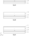
- FIG. 1A is a partial and schematic view, in cross-section, of a passivated planar photodiode 1 according to one embodiment, belonging to a matrix of photodiodes.
- the photodiodes 1 are made from germanium, and are reverse-polarized from the first surface 10a, while being isolated from each other by trenches filled with a p+ doped semiconductor material. They each comprise an intercalated semiconductor portion 27 located here between and in contact with a metal electrical polarization contact 32.1 and the first n+ doped region 11.
- a three-dimensional direct reference frame XYZ is defined, where the X and Y axes form a plane parallel to the main plane of the photodiode 1, and where the Z axis is oriented along the thickness of the detection portion 1 of the photodiode, from the second surface 10b in the direction of the first surface 10a.
- the photodiode 1 comprises a detection portion 10 extending along the Z axis between a first and a second reference surface 10a and 10b, parallel to each other and opposite to each other.
- the first surfaces 10a of the photodiodes are parallel between them, and the second surfaces 10b are also parallel to each other.
- the first surface 10a is defined by a part of the detection portion 10 where the first n+ doped region 11 and the intermediate region 13 are flush.
- the second surface 10b is opposite the first surface 10a along the Z axis.
- the maximum thickness of the detection portion 10, defined along the Z axis between the first and second surfaces 10a, 10b, is here substantially constant from one photodiode to another, for example is between a few hundred nanometers and a few microns, for example between approximately 1 ⁇ m and 5 ⁇ m. The thickness is chosen so as to obtain good absorption in the wavelength range of the light radiation to be detected.
- the detection portion 10 has a transverse dimension in the XY plane which can be between a few hundred nanometers and a few tens of microns, for example between approximately 1 ⁇ m and 20 ⁇ m.
- the detection portion 10 is made of a crystalline, preferably monocrystalline, germanium-based semiconductor material.
- germanium-based it is meant that the crystalline semiconductor material corresponds to germanium or is a compound formed of at least germanium.
- the photodiodes can be made, for example, of germanium Ge, silicon germanium SiGe, germanium tin GeSn, or even silicon germanium tin SiGeSn.
- the detection portion 10 is made of at least one layer made of germanium. It can thus be a layer or a substrate made of the same semiconductor material and have regions of different types of conductivity (homojunction) so as to form a PN or PIN junction. It can alternatively be a stack of sub-layers of different semiconductor materials (heterojunction), which are then formed based on germanium.
- the detection portion 10 is thus formed of a first n-type doped (n or n+) region 11, which is flush with the first surface 10a and forms an n-type doped well, and a second p+ doped region 12, which is flush with the second surface 10b.
- n or n+ n-type doped
- second p+ doped region 12 which is flush with the second surface 10b.
- An intermediate region 13 not intentionally doped (in the case of a PIN junction), or p-doped (in the case of a PN junction), is located between and in contact with the two doped regions 11 and 12, and surrounds the first n+ doped region 11 in the main plane.
- the semiconductor junction is of the PIN type, the first region 11 being n+ doped, the second region 12 p+ doped and the intermediate region 13 is intrinsic (not intentionally doped).
- the first n-type doped region 11 here extends from the first surface 10a and is surrounded by the intrinsic region 13 in the main plane. It is distant from the lateral edge 10c of the detection portion 10 in the XY plane, the lateral edge 10c being defined by the internal face of a p+ doped peripheral semiconductor portion 25. It thus forms an n+ doped well which is flush with the first surface 10a and is spaced of a non-zero distance from the lateral edge 10c as well as from the second surface 10b.
- the first n+ doped region 11 thus participates in delimiting the first surface 10a. It can have a doping which can be between 5.10 18 and 10 21 at/cm 3 approximately.
- the second p+ doped region 12 extends in the XY plane, flush with the second surface 10b, here from the lateral edge 10c. It extends along the Z axis from the second surface 10b. It may have a substantially uniform thickness along the Z axis and thus be flush with only a lower zone of the lateral edge 10c.
- the second p+ doped region 12 may have a p+ doped lateral region 14 which is continuously flush with the lateral edge 10c along the Z axis and extends over the entire periphery of the detection portion 10.
- the second p+ doped region 12 may have a doping which may be between approximately 10 18 and 10 19 at/cm 3 .
- the intermediate region 13 is located between the two n+ and p+ doped regions 11, 12, and surrounds the first n+ doped region 11 in the XY plane. It is here made of an intrinsic semiconductor material so as to form a PIN junction but can be weakly p-doped, to form a PN junction (cf. Fig. 1B ).
- the photodiode 1 here comprises a lower insulating layer 21, made of a dielectric material, covering the second surface 10b of the detection portion 10, as well as, as described later, the lower face of the p+-doped peripheral semiconductor portion 25.
- the lower insulating layer 21 may further be adapted to form an anti-reflection function with respect to the incident light radiation. It in fact forms the receiving face of the light radiation intended to be detected.
- the detection portion 10 of the photodiode 1 is here delimited laterally, in the XY plane, by a trench, preferably continuous, filled with a p+ doped semiconductor material, and forming a peripheral semiconductor portion 25, here p+ doped.
- the peripheral through portion 25 participates in electrically polarizing the photodiode 1, here from the side of the first surface 10a, and in pixelating the photodiode matrix (optical isolation). It extends here over the entire thickness of the detection portion 10 to open onto the lower insulating layer 21, but alternatively, it may not open onto the lower insulating layer 21 and may end in the second p+ doped region 12.
- the internal face of this p+ doped peripheral semiconductor portion 25 then defines the lateral edge 10c of the detection portion 10.
- the semiconductor material is preferably made from silicon, for example amorphous silicon, polycrystalline silicon, silicon germanium, or can even be made from amorphous germanium.
- An upper insulating layer 23 covers the first surface 10a of the photodiode 1, and makes it possible to electrically insulate the metal contacts 32.1 and 32.2. It is thus in contact with the first n+ doped region 11 as well as the intermediate region 13. It is made of a dielectric material, such as silicon oxide, silicon nitride, or silicon oxynitride. Other dielectric materials can be used, such as hafnium or aluminum oxide, or even aluminum nitride, among others. It has a thickness, for example, between 50nm and 500nm.
- the detection portion 10 advantageously comprises a p+ doped lateral region 14 located at the lateral edge 10c.
- This lateral region 14 has a doping level higher than that of the intermediate region 13 when it is doped.
- the p+ doped lateral region 14 is flush with the lateral edge 10c and is in contact with the p+ doped peripheral semiconductor portion 25.
- the polarization of the second p+ doped region 12 is improved to the extent that the contact surface with the p+ doped peripheral semiconductor portion 25 is increased.
- this p+ doped lateral region 14 makes it possible to prevent the space charge zone of the photodiode 1 from extending as far as the lateral edge 10c.
- the contribution of this zone (potentially not free from defects linked to the production of the trenches) to the dark current is limited. This improves the performance of photodiode 1.
- the detection portion 10 is made from germanium, for example is made from germanium, and the p+-doped peripheral semiconductor portion 25 is made from silicon, for example doped polycrystalline silicon.
- the detection portion 10 then advantageously comprises a lateral zone 15 made from silicon germanium.
- the lateral zone 15 is flush with the lateral edge 10c and is in contact with the p+-doped peripheral semiconductor portion 25.
- the lateral zone 15 has a bandgap energy greater than that of the detection portion 10 made from germanium.
- This lateral “gap opening” makes it possible to reduce the sensitivity of the photodiode 1 to defects present near the trenches. This also improves the performance of the photodiode 1.
- the photodiode 1 comprises an intercalated semiconductor portion 27, arranged on and in contact with the first n+ doped region 11. It is spaced by a non-zero distance from the peripheral semiconductor portions 25 in the XY plane and is here surrounded by the upper insulating layer 23. It is made of a crystalline semiconductor material doped here of the n+ type, which has a natural lattice parameter equal to within 1%, and preferably to within 0.5%, of that of the crystalline semiconductor material of the detection portion 10, here germanium, and has a band gap energy greater by at least 0.5eV than that of the crystalline semiconductor material of the detection portion 10 (germanium).
- the intercalated semiconductor portion 27 can thus be made of a III-V binary or ternary compound, such as GaAs, AlAs, GaAlAs, GaInP, among others.
- the intermediate semiconductor portion 27 is advantageously located in a notch formed in the first surface 10a of the detection portion. 10, which makes it possible to reduce or even avoid the presence of structural defects (dislocations) in the intercalated portion 27, as described later. Alternatively, it can rest on the first surface 10a which is then continuously flat (no notch).
- the size in the XY plane of the intercalated semiconductor portion 27 depends on the size of the photodiode 1: for a photodiode with a pitch of 5 ⁇ m, it can be between approximately 0.5 and 4 ⁇ m (and preferably less than 2 ⁇ m), and for a pitch of 10 ⁇ m, it can be between approximately 1 and 9 ⁇ m.
- the intercalated semiconductor portion 27 comprises n-type dopants identical to those present in the first n+ doped region 11, insofar as, as explained below, the formation of the first region 11 is carried out by diffusion of the dopants through the intercalated semiconductor portion 27 (cf. fig.2A to 2L ) or initially contained in the intercalated semiconductor portion 27 ( fig.3A to 3C ).
- the photodiode 1 further comprises metal contacts 32.1, 32.2 allowing it to be reverse-biased from the side of the first surface 10a.
- a metal contact 32.1 is here arranged on and in contact with the intermediate semiconductor portion 27, and allows the first n+ doped region 11 to be electrically polarized.
- a metal contact 32.2 is here arranged on and in contact with the peripheral semiconductor portion 25, and allows the second p+ doped region 12 to be electrically polarized.
- the metal contacts 32.1, 32.2 are here electrically isolated from each other in the XY plane by the upper insulating layer 23 and by a passivation dielectric layer 29.
- the photodiode 1 is intended to be reverse biased, for example by applying a negative electrical potential to the p+ doped peripheral semiconductor portion 25 and by bringing the first n+ doped region 11 to ground.
- the photodiode 1 may have dimensions in the XY plane of between approximately 1 ⁇ m and 100 ⁇ m.
- the thickness of the second p+ doped region 12 may be between approximately 20 nm and 500 nm.
- the thickness of the intrinsic region 13 may be between approximately 0.7 ⁇ m and 2.5 ⁇ m when the photodiode 1 is intended to detect light radiation in the SWIR or near infrared (NIR) range.
- the first n+ doped region 11 may have a thickness of between approximately 10 nm and 600 nm.
- the dielectric layers 23 and 29 may together have a thickness enabling the upper face of the photodiode 1 to be completely covered, for example between approximately 10 nm and 600 nm, and the thickness of the lower insulating layer 21 may be between approximately 50 nm and 1 ⁇ m.
- the photodiode 1 has improved performance compared to the examples of the prior art mentioned previously. Indeed, the photodiode 1, by the presence of the intermediate semiconductor portion 27 located between the metal contact 32.1 and the n-doped germanium 11, does not have a metal contact on the n-doped germanium
- the intercalated semiconductor portion 27, which is in contact with the first n+ doped region 11, is made of a semiconductor material with a band gap energy at least 0.5eV higher than that of germanium, which makes it possible to reduce the dark current of the photodiode 1 on the one hand, and to reduce the sensitivity of the photodiode 1 to defects possibly present near the notch in which the intercalated semiconductor portion 27 is located.
- FIG. 1B is a schematic and partial view, in cross-section, of a photodiode 1 according to an alternative embodiment.
- the photodiode 1 differs from that illustrated in the fig.1A in particular in that the intermediate region 13 is weakly p-doped (PN junction), and in that an upper semiconductor portion 28 is located between and in contact with the central metal contact 32.1 and the intermediate semiconductor portion 27.
- PN junction weakly p-doped
- the intercalated semiconductor portion 27 rests on and in contact with the detection portion 10. It is thus in contact with the first n+ doped region 11. It is made of a crystalline semiconductor material having the properties mentioned above in terms of band gap energy and absence of lattice mismatch with the germanium of the detection portion 10. As indicated below, it was made by epitaxy from germanium and in an unintentionally doped manner.
- the upper semiconductor portion 28 therefore rests on and in contact with the intercalary semiconductor portion 27. It is spaced from the peripheral semiconductor portion 25 and the metal contacts 32.2 in the XY plane by a non-zero distance. This lateral space is filled here by the passivation dielectric layer 29.
- the upper semiconductor portion 28 is made of an n+ doped semiconductor material, with dopants capable of n+ doping the germanium to form the first n+ doped region 11, here with phosphorus or arsenic.
- the upper semiconductor portion 28 is a reservoir of dopants intended to diffuse, during diffusion annealing, through the intercalary semiconductor portion 27 to join the germanium and form the first n+ doped region 11. It is preferably made from polycrystalline silicon, but other polycrystalline materials can of course be used.
- the metal contact 32.1 is here arranged on and in contact with the upper semiconductor portion 28. It makes it possible to electrically polarize the first n+ doped region 11 via the upper semiconductor portion 28 then the intermediate semiconductor portion 27.
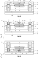
- FIGS. 2A to 2L are schematic and partial views, in cross-section, of different stages of a method of manufacturing a photodiode according to the example of the fig.1B .
- This method has the particular advantage of producing the metal contacts 32.1 and 32.2 simultaneously. It also has the advantage of not doping the intercalated semiconductor portion 27 during growth (controlling the diffusion of the dopants can be tricky) or by ion implantation (which can create defects in the intercalated semiconductor portion 27).
- the photodiodes 1 are made of germanium and have a PIN junction, and are adapted to detect infrared radiation in the SWIR range.
- the photodiodes 1 are planar and passivated, and are reverse biased from the first surface 10a, and here by means of a control chip 40 hybridized to the photodiode matrix 1.
- a first semiconductor sub-layer 22.1 of monocrystalline germanium is produced.
- the first semiconductor sub-layer 22.1 is secured to a support layer 20, here made of silicon, via a lower insulating layer 21, here made of silicon oxide.
- This stack takes the form of a GeOI substrate (for Germanium On Insulator, in English).
- This stack is preferably produced using the method described in the publication of Reboud et al. entitled Structural and optical properties of 200mm germanium-on-insulator (GeOI) substrates for silicon photonics applications, Proc. SPIE 9367, Silicon Photonics X, 936714 (February 27, 2015 ).
- Such a method has the advantage of producing a germanium 22.1 semiconductor sub-layer having a total absence or a low rate of structural defects such as dislocations.
- the germanium may be unintentionally doped or be doped, for example p-type.
- the semiconductor sub-layer 22.1 may have a thickness of between approximately 100nm and 500nm, for example equal to approximately 300nm, and may be covered with a protective layer (not shown) made of a silicon oxide.
- the lower insulating layer 21 (BOX, for Buried Oxide, in English) may have a thickness of between 50nm and 1 ⁇ m, for example between 100nm and 500nm, and advantageously provides an anti-reflection function.
- the first sub-layer 22.1 is then doped with p+-doped germanium by ion implantation of a dopant such as boron or gallium, when the first sub-layer 22.1 was initially made of intrinsic germanium.
- a dopant such as boron or gallium
- the protective layer if any, was previously removed by surface cleaning, and the first sub-layer 22.1 of germanium can be coated with a pre-implantation oxide layer (not shown) with a thickness of a few tens of nanometers, for example equal to 20nm.
- the 22.1 germanium sub-layer then has a doping level of between 10 18 and 10 20 at/cm 3 approximately.
- a diffusion annealing of the dopant can then be carried out under nitrogen, for a few minutes to a few hours, for example 1h, at a temperature which can be between 600°C and 800°C, for example equal to 800°C. This annealing can not be carried out when the 22.1 sub-layer was doped at growth.
- Another way of manufacturing this p+ layer is by epitaxy of a layer of germanium doped with boron in situ between 10 18 and 10 19 at/cm 3 approximately on an intrinsic germanium sub-layer. This epitaxy can be done between 400 and 800°C but preferably at 400°C.
- a second semiconductor sub-layer 22.2 of germanium is produced by epitaxy from the first sub-layer 22.1.
- the two sub-layers 22.1, 22.2 are intended to form the coplanar detection portions 10 made of germanium of the photodiode matrix 1.
- the second sub-layer 22.2 is formed by epitaxy, for example by chemical vapor deposition (CVD) and reduced pressure chemical vapor deposition (RPCVD) or by any other epitaxy technique. Annealing may be carried out to reduce the dislocation rate in the sub-layer 22.2.
- the pre-implementation oxide layer, if any, has been previously removed by surface cleaning.
- the second sub-layer 22.2 of germanium is here intrinsic, that is to say not intentionally doped insofar as it is desired to produce a PIN junction. It is intended to form the light absorption zone of the photodiodes 1. Its thickness depends on the wavelength range of the light radiation to be detected in the case of a photodiode 1. In the context of SWIR photodiodes, the sub-layer 22.2 of intrinsic germanium has a thickness for example between 0.5 ⁇ m and 3 ⁇ m, preferably equal to 1.5 ⁇ m.
- an upper insulating layer 23 is deposited so as to continuously cover the upper face of the second sub-layer 22.2, that is to say so as to cover the detection portions 10 of the photodiodes 1.
- the upper insulating layer 23 is made of a dielectric material, for example a silicon oxide, nitride or oxynitride. Cleaning of the upper face of the second sub-layer 22.2 may have been carried out beforehand.
- the upper insulating layer 23 may have a thickness of between 10nm and 600nm.
- the trenches 24 intended to pixelate the photodiodes 1 and to participate in their reverse electrical polarization are produced by photolithography and etching (by means of the peripheral semiconductor portions 25 which will then be produced).
- a localized etching of the upper insulating layer 23, of the intrinsic germanium sub-layer 22.2, and of the germanium sub-layer 22.1 are thus carried out.
- Each trench 24 thus preferably extends continuously around a photodiode 1.
- a plurality of detection portions 10 are thus obtained, separated from each other by a continuous trench 24.
- the trenches 24 have a transverse dimension (width) in the XY plane which can be between 300nm and 2 ⁇ m, for example equal to 1 ⁇ m.
- the detection portions 10 can thus have a shape in the XY plane, for example circular, oval, polygonal, for example square, or any other shape.
- the peripheral semiconductor portions 25 are then produced.
- a doped semiconductor material is deposited so as to fill the trenches 24.
- the semiconductor material is preferably a silicon-based material, for example amorphous silicon, polycrystalline silicon, silicon germanium, or even amorphous germanium.
- the semiconductor material is doped p+ with boron or gallium, with a dopant concentration of the order of approximately 10 19 to 10 20 at/cm 3 . Thus, the doped semiconductor material comes into contact with the lateral edge 10c via the trench 24.
- a chemical mechanical polishing (CMP) step is then carried out, with a stop on the upper face of the upper insulating layer 23, to remove the excess semiconductor material and planarize the upper face formed by the upper insulating layer 23 and the semiconductor material of the peripheral semiconductor portion 25.
- CMP chemical mechanical polishing
- a dielectric layer is deposited so as to cover the upper surface of the peripheral semiconductor portions 25 (this increases the thickness of the upper insulating layer 23 which thus covers the portions 25). Then, by photolithography and etching, a through opening 26.1 is produced within the upper insulating layer 23 to open onto the detection portion 10, opposite a central zone located at a distance from the peripheral semiconductor portions 25 in the XY plane.
- the width or diameter of the through opening 26.1 depends in particular on the desired width of the first n+ doped region. It can be between 0.3 ⁇ m and 5 ⁇ m for example.
- the through opening 26.1 also forms a notch within the detection portion 10, for example with a depth of around a hundred nanometers.
- an intercalated semiconductor portion 27 is produced, located opposite the central zone of the detection portion 10 and in contact with it.
- the intercalated semiconductor portion 27 is produced by epitaxy here from the germanium of the detection portion, for example by molecular beam epitaxy (MBE, Molecular Beam Epitaxy, in English). It is made of a semiconductor material crystalline which has, on the one hand, a lattice parameter almost identical to that of germanium, that is to say that its natural lattice parameter is equal to that of germanium to at most 1.0%, and preferably to at most 0.5%; and on the other hand, a band gap energy Eg higher (that is to say strictly higher) than that Eg Ge of the germanium of the detection portion.
- MBE molecular beam epitaxy
- the intercalated semiconductor portion 27 is made of AlAs or GaAs (stoichiometric compounds, i.e. the proportion of the two elements is identical, whose natural lattice parameter is 5.6605 ⁇ for AlAs and 5.653 ⁇ for GaAs, which corresponds respectively to a deviation of 0.044% and 0.088% with the natural lattice parameter of 5.658 ⁇ of germanium.
- the band gap energy is 2.12eV for AlAs and 1.424eV for GaAs, which is much higher than the 0.67eV of germanium.
- Other semiconductor compounds, for example ternary may also be suitable, such as for example GaAlAs and GaInP depending on the proportions of the different chemical elements.
- the intercalated semiconductor portion 27 is intrinsic, i.e. not intentionally doped.
- the formation of the first n+ doped region 11 will be obtained by diffusion of germanium dopants (e.g. phosphorus or arsenic) from a dopant reservoir (the upper semiconductor portion 28) through the intercalated semiconductor portion 27).
- germanium dopants e.g. phosphorus or arsenic
- an upper semiconductor portion 28 is produced, forming the reservoir of n-type dopants intended to diffuse into the detection portion through the intermediate semiconductor portion 27 to ultimately obtain the first n+ doped region 11. It is produced from an n+ doped semiconductor material, for example polysilicon or polycrystalline silicon germanium. However, it is advantageously produced from a material identical to that of the peripheral semiconductor portion, for example here polysilicon, so as to simplify the production of the metal contacts 32.1 and 32.2.
- the upper semiconductor portion 28 is made of polysilicon doped n+ with phosphorus or arsenic, produced by low-pressure chemical vapor deposition (LPCVD) between 400°C and 650°C for example. It has a size in the XY plane preferably greater than that of the intercalary semiconductor portion 27, and a thickness of for example between 50nm and 200nm.
- LPCVD low-pressure chemical vapor deposition
- a diffusion and activation annealing of the dopants is then carried out, for example between 500°C and 800°C and for approximately 10 to 60 min.
- the dopants phosphorus or arsenic
- the dopants diffuse through the intercalated semiconductor portion 27 then into the detection portion 10.
- a first n+ doped region 11 is thus obtained which extends in contact with the intercalated semiconductor portion 27, both along the Z axis and in the XY plane.
- the intercalated semiconductor portion 27 was epitaxially grown in a notch 26.2 of the detection portion 10 makes it possible to reduce the number of structural defects (dislocations) in the intercalated semiconductor portion 27 or even to avoid them. This results in a crystalline material of better crystalline quality, which improves the performance of the photodiode.
- a passivation dielectric layer 29 is deposited so as to cover the upper semiconductor portion 28.
- the dielectric layer can be deposited at 400°C and be made of a dielectric material such as a silicon oxide, nitride or oxynitride, an aluminum oxide or nitride, a hafnium oxide, among others. It can have a thickness of, for example, between 200nm and 1000nm.
- a CMP-type planarization step is then carried out.
- Through openings 30 are then made through the dielectric layers 23, 29 so as to open onto an upper surface of the peripheral semiconductor portion 25 (to then make the metal contact 32.2) and onto an upper surface of the upper semiconductor portion 28 (to then make the metal contact 32.1).
- These through openings 30 may have a size in the XY plane of between 0.1 ⁇ m and 1 ⁇ m, preferably between 0.3 ⁇ m and 1 ⁇ m. They may be made by plasma etching with an etching stop on the polysilicon surfaces of the upper semiconductor portion 28 and the peripheral semiconductor portion 25.
- the upper portion 28 and the peripheral portion 25 are made of the same material, here silicon, makes it possible to make the metal contacts 32.1 and 32.2 simultaneously, thus simplifying the manufacturing process.
- a silicided zone 31 is preferably produced on the upper surface of the upper semiconductor portion 28, and a silicided zone 31 on the upper surface of the peripheral semiconductor portion 25.
- a thin layer of the type formed by a Ni/TiN stack with thicknesses of 9nm and 10nm is deposited at the bottom of the through openings 30, 30 by physical vapor deposition (PVD), followed by a siliciding annealing between approximately 300°C and 350°C for approximately 10 to 30s.
- PVD physical vapor deposition
- the unreacted Ni and TiN is then removed, and then a second siliciding annealing is carried out between approximately 400°C and 450°C for approximately 10 to 30s.
- the central 32.1 and lateral 32.2 metal contacts are then produced.
- a thin bonding layer 33 formed from a Ti/TiN/Cu type stack is deposited by chemical deposition in the value phase in the through openings 30.1, 30.2, and the empty space is filled with copper 34 deposited by electrolysis.
- a CMP type planarization step is then carried out with a stop on the oxide of the dielectric passivation layer 29.
- the dielectric passivation layer 29 and the metal contacts 32.1 and 32.2 together have the same planar upper face.
- the hybridization of the optoelectronic stack thus obtained is carried out on a control chip 40.
- the connection face of the control chip 40 can thus be coated with an insulating layer 41, made of a dielectric material, crossed by metal contacts 42.
- the photodiode matrix 1 and the control chip 40 are thus assembled by hybrid molecular adhesion, by contact of the faces formed by the metal contacts and the insulating layers.
- a bonding annealing can be carried out so as to increase the surface bonding energy between the two faces in contact.
- the support layer 20 is then removed, for example by abrasion ( grinding, in English), so as to expose the lower insulating layer 21. This thus forms the receiving face of the light radiation to be detected, and advantageously provides an antireflection function.
- the manufacturing method thus makes it possible to obtain one or more passivated photodiodes 1, each comprising an interposed semiconductor portion 27 in contact with the detection portion 10, the properties of which in terms of mesh parameters and band gap energy make it possible to avoid having to make a metal contact directly on the n-doped germanium, such a contact being either of the rectifier type or of the ohmic but highly resistive type.
- One or more photodiodes 1 are thus produced having improved performance, in particular in terms of low-frequency noise (as indicated previously).
- FIGS. 3A to 3C are schematic and partial views, in cross-section, of different stages of a method of manufacturing a photodiode 1 according to the example of the fig.1A .
- Photodiode 1 is different from the one illustrated in the fig.1B essentially in that it does not include an upper semiconductor portion 28. Also, the metal contact 32.1 is on and in contact with the intermediate semiconductor portion 27.
- the first n+ doped region 11 is produced by diffusion of dopants from the intermediate semiconductor portion 27 which itself forms the dopant reservoir (and not from the upper semiconductor portion 28, as in the Figures 2A to 2L ).
- the intermediate semiconductor portion 27 is produced by epitaxial growth directly from the detection portion 10. This step is similar to that of the fig.2G and is distinguished in that the intercalated semiconductor portion 27 is n+ doped with dopants suitable for n-doping the germanium of the detection portion 10, for example here with phosphorus, arsenic, or even silicon or zinc.
- the intercalated semiconductor portion 27 is doped during growth and not by ion implantation, to avoid any degradation of the crystalline quality of the material.
- the dopants do not modify the properties of the material of the portion intercalated semiconductor 27 in terms of lattice parameter.
- the band gap energy remains at least 0.5eV higher than that of the germanium of the detection portion 10.
- the epitaxy temperature is controlled to limit possible diffusion of the dopants in the detection portion 10.
- the first n+ doped region 11 is produced by performing a diffusion and activation annealing of the dopants.
- the temperature and duration of the annealing can be similar to those mentioned previously, in connection with the fig.2I .
- the dopants diffuse from the intercalated semiconductor portion 27 into the detection portion 10, which forms the first n+ doped region 11.
- the metal contacts 32.1 and 32.2 are produced.
- a through opening is produced in the insulating layers 23 and 29 which opens onto the peripheral semiconductor portion 25, then the silicided zone 31 is produced.
- a through opening is produced in the insulating layer 29 which opens onto the intermediate semiconductor portion 27.
- a thin bonding layer 33 is deposited in the openings and then the free space is filled with copper 34. This gives the metal contacts 32.1 and 32.2.
Landscapes
- Light Receiving Elements (AREA)
- Electrodes Of Semiconductors (AREA)
Description
- Le domaine de l'invention est celui des photodiodes planaires passivées réalisées à base de germanium comportant des contacts métalliques optimisés. L'invention trouve une application notamment dans le domaine de la détection d'un rayonnement lumineux dans le proche infrarouge.
- Les dispositifs optoélectroniques de photodétection peuvent comporter une matrice de photodiodes planaires passivées. Les photodiodes s'étendent alors suivant un même plan principal, entre des première et deuxième surfaces opposées et parallèles entre elles. Elles comportent alors chacune une portion de détection, formée par exemple d'une première région en germanium dopé n et affleurant la première surface, d'une deuxième région en germanium dopé p et affleurant la deuxième surface, et d'une région intermédiaire en germanium intrinsèque ou très peu dopé p, et située entre les première et deuxième régions dopées. Une couche de passivation réalisée en un matériau diélectrique peut recouvrir la première surface dans le but de limiter la contribution du courant d'obscurité au courant électrique mesuré par chaque photodiode.
- La polarisation électrique de la première région dopée n et de la deuxième région dopée p peut, dans le cas des photodiodes planaires passivées, être effectuée du côté de la première surface. Ainsi, une portion semiconductrice périphérique, par exemple réalisée en silicium polycristallin dopé p, entoure la portion de détection dans un plan principal de la photodiode et vient au contact de la deuxième région dopée p. De plus, des contacts métalliques, disposés du côté de la première surface, viennent au contact de la première région dopée n et de la portion semiconductrice périphérique dopée p.
- Cependant, il apparaît qu'un contact métallique sur du germanium dopé n est de type redresseur et non pas de type ohmique, du fait du blocage du niveau de Fermi (Fermi level pinning, en anglais) à l'interface métal / germanium. Il existe toutefois différentes solutions pour rendre ohmique le contact métal / germanium dopé n.
- Ainsi, le document de Paramahans et al. intitulé Contacts on n-type germanium using variably doped zinc oxide and highly doped indium tin oxide interfacial layers, Appl. Phys. Express 8, 051302 (2015) décrit le fait d'intercaler une très mince couche diélectrique entre le métal et le germanium dopé n, comme par exemple du ZnO d'au moins 2nm d'épaisseur ou de l'ITO d'au moins 2.4nm d'épaisseur. Par ailleurs, le document de Wu et al. intitulé Ohmic contact to n-type Ge with compositional Ti nitride, Appl. Surf. Sc. 284, 877-880 (2013) décrit une autre solution qui consiste à réaliser un contact de type TiNx/n-Ge avec x au moins égal à 0.8 pour obtenir un contact ohmique. Cependant, ces contacts ohmiques peuvent alors être très résistifs, ce qui dégrade les performances de la photodiode.
- Par ailleurs, le document
EP3657556A1 décrit une photodiode planaire passive réalisée à base de germanium, dans laquelle une portion semiconductrice intercalaire de silicium polycristallin dopé n est formée sur et au contact de la portion de détection. Elle forme un réservoir de dopants de type n destinés à diffuser dans le germanium pour réaliser la première région dopée n. Un contact métallique est réalisé sur et au contact de la portion semiconductrice intercalaire, et permet de polariser électriquement la première région dopée n. - Cependant, il existe un besoin de disposer d'une telle photodiode planaire passivée présentant des performances améliorées.
- Le document
EP3660930A1 décrit une photodiode PIN au germanium. - L'invention a pour objectif de remédier au moins en partie aux inconvénients de l'art antérieur, et plus particulièrement de proposer un photodiode planaire passivée qui présente des performances améliorées.
- Pour cela, l'objet de l'invention est une photodiode comportant :
- une portion de détection, présentant une première surface et une deuxième surface opposées l'une à l'autre et parallèles à un plan principal, réalisée en un premier matériau semiconducteur cristallin à base de germanium, comportant :
- ∘ une première région dopée de type n, et affleurant la première surface ;
- ∘ une deuxième région dopée de type p, et affleurant la deuxième surface ;
- ∘ une région intermédiaire, située entre la première région et la deuxième région et entourant la première région dans le plan principal ;
- une portion semiconductrice périphérique, réalisée en un deuxième matériau semiconducteur dopé de type p, entourant la portion de détection dans le plan principal et venant au contact de la deuxième région ;
- une portion semiconductrice intercalaire, disposée sur et au contact de la première région de la portion de détection ;
- des contacts métalliques, disposés du côté de la première surface, et adaptés à polariser électriquement, d'une part la première région par le biais de la portion semiconductrice intercalaire, et d'autre part la deuxième région par le biais de la portion semiconductrice périphérique.
- Selon l'invention, la portion semiconductrice intercalaire est réalisée en un troisième matériau semiconducteur cristallin présentant : un paramètre de maille naturel égal, à 1% près, à un paramètre de maille naturel du premier matériau semiconducteur à base de germanium ; et une énergie de bandes interdites supérieure d'au moins 0.5eV à celle du premier matériau semiconducteur à base de germanium.
- Certains aspects préférés mais non limitatifs de cette photodiode sont les suivants.
- La portion semiconductrice intercalaire peut comporter des dopants de type n identiques à ceux présents dans la première région.
- La portion semiconductrice intercalaire peut être réalisée en un composé semiconducteur cristallin III-V, et de préférence en AlAs ou en GaAs.
- La portion semiconductrice intercalaire peut être située dans une échancrure de la première surface de la portion de détection, de sorte que la portion semiconductrice intercalaire est entourée, dans le plan principal par la première région.
- L'un des contacts métalliques, dit contact métallique central, peut être situé sur et au contact de la portion semiconductrice intermédiaire.
- La photodiode peut comporter une portion semiconductrice supérieure située sur et au contact de la portion semiconductrice intercalaire, réalisée en un matériau semiconducteur dopé de type n avec des dopants identiques à ceux de la portion semiconductrice intercalaire et de la première région.
- L'un des contacts métalliques, dit contact métallique central, peut alors être situé sur et au contact de la portion semiconductrice supérieure.
- La portion semiconductrice supérieure peut être réalisée en un matériau identique à celui de la portion semiconductrice périphérique.
- La portion semiconductrice supérieure et la portion semiconductrice périphérique peuvent être réalisées en un matériau semiconducteur à base de silicium. La photodiode peut alors comporter une zone supérieure siliciurée au contact avec les contacts métalliques.
- L'invention porte également sur un procédé de fabrication d'une photodiode selon l'une quelconque des caractéristiques précédentes, comportant les étapes suivantes
- réalisation d'un empilement comportant une première sous-couche destinée à former la deuxième région et une deuxième sous-couche destinée à former la région intermédiaire ;
- réalisation d'une couche isolante supérieure recouvrant l'empilement ;
- réalisation de la portion semiconductrice périphérique au travers de l'empilement et de la couche isolante supérieure pour déboucher sur la première sous-couche ;
- réalisation de la portion semiconductrice intercalaire par épitaxie à partir de la deuxième sous-couche de l'empilement, au travers d'une ouverture de la couche isolante supérieure.
- Le procédé peut comporter, avant l'étape de réalisation de la portion semiconductrice intercalaire, une étape de réalisation d'une échancrure dans la deuxième sous-couche de l'empilement, au travers de l'ouverture, suivie de l'épitaxie de la portion semiconductrice intercalaire dans l'échancrure.
- Lorsque la portion semiconductrice intercalaire est non intentionnellement dopée lors de son épitaxie, le procédé peut alors comporter les étapes suivantes :
- réalisation de la portion semiconductrice supérieure dopée de type n ;
- recuit adapté à provoquer la diffusion des dopants contenus dans la portion semiconductrice supérieure au travers de la portion semiconductrice intercalaire pour former la première région dans la portion de détection.
- La portion semiconductrice supérieure et la portion semiconductrice périphérique peuvent être réalisées en un même matériau à base de silicium. Le procédé peut alors comporter une étape de réalisation des contacts métalliques de manière simultanée, l'un au contact de la portion semiconductrice supérieure, et l'autre au contact de la portion semiconductrice périphérique.
- La portion semiconductrice intercalaire peut être dopée de type n lors de son épitaxie. Le procédé peut alors comporter l'étape suivante : réalisation des contacts métalliques, l'un au contact de la portion semiconductrice intercalaire, et l'autre au contact de la portion semiconductrice périphérique.
- D'autres aspects, buts, avantages et caractéristiques de l'invention apparaîtront mieux à la lecture de la description détaillée suivante de formes de réalisation préférées de celle-ci, donnée à titre d'exemple non limitatif, et faite en référence aux dessins annexés sur lesquels :
- la
figure 1A est une vue schématique et partielle, en coupe transversale, d'une photodiode planaire passivée selon un mode de réalisation, comportant un contact métallique au contact de la portion semiconductrice intercalaire, laquelle est au contact de la première région de la portion de détection ; - la
figure 1B est une vue schématique et partielle, en coupe transversale, d'une photodiode planaire passivée selon une variante de réalisation, comportant une portion semiconductrice supérieure, disposée entre et au contact du contact métallique et de la portion semiconductrice intercalaire ; - les
figures 2A à 2L illustrent différentes étapes d'un procédé de fabrication d'une photodiode selon le mode de réalisation illustré sur lafig.1B ; - les
figures 3A à 3C illustrent différentes étapes d'un procédé de fabrication d'une photodiode selon le mode de réalisation illustré sur lafig.1A . - Sur les figures et dans la suite de la description, les mêmes références représentent les éléments identiques ou similaires. De plus, les différents éléments ne sont pas représentés à l'échelle de manière à privilégier la clarté des figures. Par ailleurs, les différents modes de réalisation et variantes ne sont pas exclusifs les uns des autres et peuvent être combinés entre eux. Sauf indication contraire, les termes « sensiblement », « environ », « de l'ordre de » signifient à 10% près, et de préférence à 5% près. Par ailleurs, les termes « compris entre ... et ... » et équivalents signifient que les bornes sont incluses, sauf mention contraire.
- L'invention porte sur d'une manière générale sur une photodiode planaire passivée, et de préférence sur une matrice de photodiodes, ainsi que sur le procédé de fabrication. Chaque photodiode comporte une portion de détection réalisée à base de germanium, et est adaptée à détecteur un rayonnement lumineux dans le proche infrarouge (SWIR, pour Short Wavelength IR, en anglais) correspondant à la gamme spectrale allant de 0.8µm à 1.7µm environ, voire à 2.5µm environ.
- La portion de détection des photodiodes présente une première surface et une deuxième surface opposées l'une à l'autre et parallèles à un plan principal des photodiodes. Les deux surfaces s'étendent suivant des plans identiques pour chacune des photodiodes, et délimitent verticalement (suivant l'axe d'épaisseur) la portion de détection. Les photodiodes ne présentent pas une structure en mesa dans la mesure où elles sont isolées optiquement les unes des autres par des tranchées périphériques remplies par un matériau semiconducteur dopé. Elles présentent ainsi un facteur de remplissage particulièrement élevé. Par ailleurs, elles sont dites passivées dans la mesure où la première surface est en partie recouverte par une couche diélectrique de passivation. Celle-ci contribue à réduire la composante de surface du courant d'obscurité.
- D'une manière générale, la photodiode comporte :
- ∘ une portion de détection, réalisée en un premier matériau semiconducteur cristallin à base de germanium, et comportant : une première région dopée de type n, une deuxième région dopée de type p, et une région intermédiaire située entre les deux régions dopées et entourant la première région dopée dans un plan principal de la photodiode ;
- ∘ une portion semiconductrice périphérique, réalisée en un deuxième matériau semiconducteur dopé p, entourant la portion de détection dans le plan principal et venant au contact de la deuxième région dopée ;
- ∘ une portion semiconductrice intercalaire, disposée sur et au contact de la première région dopée n, et réalisée en un matériau semiconducteur cristallin, dopé n, et venant au contact de la première région dopée n ;
- ∘ des contacts métalliques, disposés du côté de la première surface, et adaptés à polariser électriquement, d'une part la première région par le biais de la portion semiconductrice intercalaire, et d'autre part, la deuxième région par le biais de la portion semiconductrice périphérique.
- Le matériau semiconducteur cristallin de la portion semiconductrice intercalaire présente un paramètre de maille naturel égal à celui du premier matériau semiconducteur à base de germanium à 1% près, c'est-à-dire qu'il est égal à plus ou moins 1%, et de préférence à 0.5% près. Par paramètre de maille naturel, on entend le paramètre de maille du matériau non contraint, c'est-à-dire relaxé. Le paramètre de maille dont il est question ici est orienté dans le plan principal de la photodiode. De plus, le matériau semiconducteur cristallin de la portion semiconductrice intercalaire présente une énergie de bandes interdites supérieure d'au moins 0.5eV à celle du premier matériau semiconducteur à base de germanium. L'énergie de bandes interdites correspond à la différence d'énergie entre le minimum d'énergie de la bande de conduction et le maximum d'énergie de la bande de valence. Le matériau semiconducteur cristallin de la portion semiconductrice intercalaire est de préférence un composé III-V, par exemple un composé III-V binaire tel que de l'AlAs et du GaAs, voire un composé III-V ternaire tel que du GaAlAs ou du GaInP.
- La
figure 1A est une vue partielle et schématique, en coupe transversale, d'une photodiode planaire passivée 1 selon un mode de réalisation, appartenant à une matrice de photodiodes. Les photodiodes 1 sont réalisées à base de germanium, et sont polarisées en inverse à partir de la première surface 10a, tout en étant isolées les unes des autres par des tranchées remplies d'un matériau semiconducteur dopé p+. Elles comportent chacune une portion semiconductrice intercalaire 27 située ici entre et au contact d'un contact métallique 32.1 de polarisation électrique et de la première région 11 dopée n+. - On définit ici et pour la suite de la description un repère direct tridimensionnel XYZ, où les axes X et Y forment un plan parallèle au plan principal de la photodiode 1, et où l'axe Z est orienté suivant l'épaisseur de la portion de détection 1 de la photodiode, à partir de la deuxième surface 10b en direction de la première surface 10a.
- La photodiode 1 comporte une portion de détection 10 s'étendant suivant l'axe Z entre une première et une deuxième surfaces de référence 10a et 10b, parallèles entre elles et opposées l'une à l'autre. Les premières surfaces 10a des photodiodes sont parallèles entre elles, et les deuxièmes surfaces 10b sont également parallèles entre elles. La première surface 10a est définie par une partie de la portion de détection 10 où affleurent la première région 11 dopée n+ ainsi que la région intermédiaire 13. La deuxième surface 10b est opposée à la première surface 10a suivant l'axe Z.
- L'épaisseur maximale de la portion de détection 10, définie suivant l'axe Z entre les première et deuxième surfaces 10a, 10b est ici sensiblement constante d'une photodiode à l'autre, par exemple est comprise entre quelques centaines de nanomètres et quelques microns, par exemple entre 1µm et 5µm environ. L'épaisseur est choisie de manière à obtenir une bonne absorption dans la gamme de longueurs d'onde du rayonnement lumineux à détecter. La portion de détection 10 présente une dimension transversale dans le plan XY pouvant être comprise entre quelques centaines de nanomètres et quelques dizaines de microns, par exemple comprise entre 1µm et 20µm environ.
- La portion de détection 10 est réalisée en un matériau semiconducteur cristallin, de préférence monocristallin, à base de germanium. Par à base de germanium, on entend que le matériau semiconducteur cristallin correspond au germanium ou est un composé formé d'au moins le germanium. Ainsi, les photodiodes peuvent être réalisées, par exemple, en germanium Ge, en silicium germanium SiGe, en germanium étain GeSn, voire en silicium germanium étain SiGeSn. Dans cet exemple, la portion de détection 10 est issue d'au moins une couche réalisée en germanium. Elle peut ainsi être une couche ou un substrat réalisé en le même matériau semiconducteur et présenter des régions de différents types de conductivité (homojonction) de manière à former une jonction PN ou PIN. Elle peut en variante être un empilement de sous-couches de différents matériaux semiconducteurs (hétérojonction), lesquels sont alors formés à base de germanium.
- La portion de détection 10 est ainsi formée d'une première région 11 dopée de type n (n ou n+), qui affleure la première surface 10a et forme un caisson dopé de type n, et une deuxième région 12 dopée p+, qui affleure la deuxième surface 10b. Par affleurer, on entend « arriver au niveau de », ou « s'étend à partir de ». Une région intermédiaire 13 non intentionnellement dopé (dans le cas d'une jonction PIN), ou dopée p (dans le cas d'une jonction PN), est située entre et au contact des deux régions dopées 11 et 12, et entoure la première région 11 dopée n+ dans le plan principal. Dans cet exemple, la jonction semiconductrice est de type PIN, la première région 11 étant dopée de type n+, la deuxième région 12 dopée de type p+ et la région intermédiaire 13 est intrinsèque (non intentionnellement dopée).
- La première région 11 dopée de type n s'étend ici à partir de la première surface 10a et est entourée par la région intrinsèque 13 dans le plan principal. Elle est distante de la bordure latérale 10c de la portion de détection 10 dans le plan XY, la bordure latérale 10c étant définie par la face interne d'une portion semiconductrice périphérique 25 dopée p+. Elle forme ainsi un caisson dopé n+ qui affleure la première surface 10a et est espacée d'une distance non nulle vis-à-vis de la bordure latérale 10c ainsi que de la deuxième surface 10b. La première région 11 dopée n+ participe ainsi à délimiter la première surface 10a. Elle peut présenter un dopage pouvant être compris entre 5.1018 et 1021 at/cm3 environ.
- La deuxième région 12 dopée p+ s'étend dans le plan XY en affleurant la deuxième surface 10b, ici à partir de la bordure latérale 10c. Elle s'étend suivant l'axe Z à partir de la deuxième surface 10b. Elle peut présenter une épaisseur sensiblement homogène suivant l'axe Z et ainsi affleurer uniquement une zone inférieure de la bordure latérale 10c. En variante, comme illustré sur les
fig.1A et 1B , la deuxième région 12 dopée p+ peut présenter une région latérale 14 dopée p+ qui affleure continûment la bordure latérale 10c suivant l'axe Z et s'étend sur toute la périphérie de la portion de détection 10. La deuxième région 12 dopée p+ peut présenter un dopage pouvant être compris entre 1018 et 1019 at/cm3 environ. - La région intermédiaire 13 est située entre les deux régions 11, 12 dopées n+ et p+, et entoure la première région 11 dopée n+ dans le plan XY. Elle est ici réalisée en un matériau semiconducteur intrinsèque de manière à former une jonction PIN mais peut être faiblement dopée p, pour former une jonction PN (cf.
fig. 1B ). - La photodiode 1 comporte ici une couche isolante inférieure 21, réalisée en un matériau diélectrique, recouvrant la deuxième surface 10b de la portion de détection 10, ainsi que, comme décrit plus loin, la face inférieure de la portion semiconductrice périphérique 25 dopée p+. La couche isolante inférieure 21 peut en outre être adaptée à former une fonction d'antireflet vis-à-vis du rayonnement lumineux incident. Elle forme en effet la face de réception du rayonnement lumineux destiné à être détecté.
- La portion de détection 10 de la photodiode 1 est ici délimitée latéralement, dans le plan XY, par une tranchée, de préférence continue, remplie d'un matériau semiconducteur dopé p+, et formant une portion semiconductrice périphérique 25, ici dopée p+. La portion traversante périphérique 25 participe à polariser électriquement la photodiode 1, ici à partir du côté de la première surface 10a, et à pixelliser la matrice de photodiodes (isolation optique). Elle s'étend ici sur toute l'épaisseur de la portion de détection 10 pour déboucher sur la couche isolante inférieure 21, mais en variante, elle peut ne pas déboucher sur la couche isolante inférieure 21 et peut se terminer dans la deuxième région 12 dopée p+. La face interne de cette portion semiconductrice périphérique 25 dopée p+ définit alors la bordure latérale 10c de la portion de détection 10. Le matériau semiconducteur est de préférence réalisé à base de silicium, par exemple du silicium amorphe, du silicium polycristallin, du silicium germanium, voire peut être réalisé en germanium amorphe.
- Une couche isolante supérieure 23 recouvre la première surface 10a de la photodiode 1, et permet d'isoler électriquement les contacts métalliques 32.1 et 32.2. Elle est ainsi au contact de la première région 11 dopée n+ ainsi que de la région intermédiaire 13. Elle est réalisée en un matériau diélectrique, tel qu'un oxyde de silicium, un nitrure de silicium, ou un oxynitrure de silicium. D'autres matériaux diélectriques peuvent être utilisés, tels qu'un oxyde d'hafnium ou d'aluminium, voire un nitrure d'aluminium, entre autres. Elle présente une épaisseur par exemple comprise entre 50nm et 500nm.
- Par ailleurs, la portion de détection 10 comporte avantageusement une région latérale 14 dopée de type p+ située au niveau de la bordure latérale 10c. Cette région latérale 14 présente un niveau de dopage supérieur à celui de la région intermédiaire 13 lorsqu'elle est dopée. La région latérale 14 dopée p+ affleure la bordure latérale 10c et est au contact de la portion semiconductrice périphérique 25 dopée p+. Ainsi, la polarisation de la deuxième région 12 dopée p+ est améliorée dans la mesure où la surface de contact avec la portion semiconductrice périphérique 25 dopée p+ est augmentée. De plus, cette région latérale 14 dopée p+ permet d'éviter que la zone de charge d'espace de la photodiode 1 ne s'étende jusqu'à la bordure latérale 10c. Ainsi, on limite la contribution de cette zone (potentiellement non exempte de défauts liés à la réalisation des tranchées) au courant d'obscurité. On améliore ainsi les performances de la photodiode 1.
- Par ailleurs, la portion de détection 10 est réalisée à base de germanium, par exemple est en germanium, et la portion semiconductrice périphérique 25 dopée p+ est réalisée à base de silicium, par exemple en silicium polycristallin dopé. La portion de détection 10 comporte alors avantageusement une zone latérale 15 réalisée à base de silicium germanium. La zone latérale 15 affleure la bordure latérale 10c et est au contact de la portion semiconductrice périphérique 25 dopée p+. Ainsi, la zone latérale 15 présente une énergie de bande interdite (gap) supérieure à celle de la portion de détection 10 réalisée en germanium. Cette « ouverture de gap » latérale permet de diminuer la sensibilité de la photodiode 1 aux défauts présents à proximité des tranchées. On améliore ainsi également les performances de la photodiode 1.
- Par ailleurs, la photodiode 1 comporte une portion semiconductrice intercalaire 27, disposée sur et au contact de la première région 11 dopée n+. Elle est espacée d'une distance non nulle des portions semiconductrice périphérique 25 dans le plan XY et est ici entourée par la couche isolante supérieure 23. Elle est réalisée en un matériau semiconducteur cristallin dopé ici de type n+, qui présente un paramètre de maille naturel égal à 1% près, et de préférence à 0.5% près, à celui du matériau semiconducteur cristallin de la portion de détection 10, ici du germanium, et présente une énergie de bandes interdites supérieure d'au moins 0.5eV à celui du matériau semiconducteur cristallin de la portion de détection 10 (germanium). La portion semiconductrice intercalaire 27 peut ainsi être réalisée en un composé binaire ou ternaire III-V, tel que du GaAs, AlAs, GaAlAs, GaInP, entre autres.
- Dans cet exemple, la portion semiconductrice intercalaire 27 est avantageusement située dans une échancrure formée dans la première surface 10a de la portion de détection 10, ce qui permet de réduire voire d'éviter la présence de défauts structuraux (dislocations) dans la portion intercalaire 27, comme décrit plus loin. En variante, elle peut reposer sur la première surface 10a qui est alors continûment plane (pas d'échancrure). La taille dans le plan XY de la portion semiconductrice intercalaire 27 dépend de la taille de la photodiode 1 : pour une photodiode de 5µm de pas, elle peut être comprise entre 0.5 et 4µm environ (et de préférence inférieure à 2µm), et pour un pas de 10µm, elle peut être comprise entre 1 et 9µm environ.
- On note ici que la portion semiconductrice intercalaire 27 comporte des dopants de type n identiques à ceux présents dans la première région 11 dopée n+, dans la mesure où, comme explicité plus loin, la formation de la première région 11 est effectuée par diffusion des dopants au travers de la portion semiconductrice intercalaire 27 (cf.
fig.2A à 2L ) ou initialement contenus dans la portion semiconductrice intercalaire 27 (fig.3A à 3C ). - La photodiode 1 comporte en outre des contacts métalliques 32.1, 32.2 permettant de la polariser en inverse à partir du côté de la première surface 10a. Ainsi, un contact métallique 32.1 est ici disposé sur et au contact de la portion semiconductrice intercalaire 27, et permet de polariser électriquement la première région 11 dopée n+. Un contact métallique 32.2 est ici disposé sur et au contact de la portion semiconductrice périphérique 25, et permet de polariser électriquement la deuxième région 12 dopée p+. Les contacts métalliques 32.1, 32.2 sont ici isolés électriquement les uns des autres dans le plan XY par la couche isolante supérieure 23 et par une couche diélectrique de passivation 29. La photodiode 1 est destinée à être polarisée en inverse, par exemple en appliquant un potentiel électrique négatif à la portion semiconductrice périphérique 25 dopée p+ et en portant la première région 11 dopée n+ à la masse.
- D'une manière générale, à titre illustratif, la photodiode 1 peut présenter des dimensions dans le plan XY comprises entre 1µm et 100µm environ. L'épaisseur de la deuxième région 12 dopée p+ peut être comprise entre 20nm et 500nm environ. L'épaisseur de la région intrinsèque 13 peut être comprise entre 0.7µm et 2.5µm environ lorsque la photodiode 1 est destinée à détecter un rayonnement lumineux dans la gamme du SWIR ou du proche infrarouge (NIR). La première région 11 dopée n+ peut présenter une épaisseur comprise entre 10nm et 600nm environ. Les couches diélectriques 23 et 29 peuvent présenter ensemble une épaisseur permettant de recouvrir entièrement la face supérieure de la photodiode 1, par exemple comprise entre 10nm et 600nm environ, et l'épaisseur de la couche isolante inférieure 21 peut être comprise entre 50nm et 1µm environ.
- Ainsi, la photodiode 1 présente des performances améliorées vis-à-vis des exemples de l'art antérieur mentionnés précédemment. En effet, la photodiode 1, par la présence de la portion semiconductrice intercalaire 27 située entre le contact métallique 32.1 et le germanium 11 dopé n, ne comporte pas de contact métallique sur le germanium dopé n
- (première région) qui formerait alors un contact redresseur, voire un contact ohmique fortement résistif. On limite ainsi les résistances séries, ce qui permet notamment de limiter le bruit de basse fréquence. De plus, la portion semiconductrice intercalaire 27, qui est au contact de la première région 11 dopée n+, est réalisée en un matériau semiconducteur d'énergie de bandes interdites supérieure d'au moins 0.5eV à celle du germanium, ce qui permet réduire le courant d'obscurité de la photodiode 1 d'une part, et de diminuer la sensibilité de la photodiode 1 aux défauts éventuellement présents à proximité de l'échancrure dans laquelle est située la portion semiconductrice intercalaire 27. De plus, l'absence de désaccord du paramètre de maille entre le matériau cristallin de la portion semiconductrice intercalaire 27 et celui de la portion de détection 10 permet d'éviter les défauts structuraux (dislocations...) qui viendraient dégrader les performances de la photodiode 1.
- La
figure 1B est une vue schématique et partielle, en coupe transversale, d'une photodiode 1 selon une variante de réalisation. Dans cet exemple, la photodiode 1 se distingue de celle illustrée sur lafig.1A notamment en ce que la région intermédiaire 13 est faiblement dopée p (jonction PN), et en ce qu'une portion semiconductrice supérieure 28 est située entre et au contact du contact métallique central 32.1 et de la portion semiconductrice intercalaire 27. - Plus précisément, la portion semiconductrice intercalaire 27, comme indiqué précédemment, repose sur et au contact de la portion de détection 10. Elle est ainsi au contact de la première région 11 dopée n+. Elle est réalisée en un matériau semiconducteur cristallin présentant les propriétés mentionnées plus haut en termes d'énergie de bandes interdites et d'absence de désaccord de maille avec le germanium de la portion de détection 10. Comme indiqué plus loin, elle a été réalisée par épitaxie à partir du germanium et de manière non intentionnellement dopée.
- La portion semiconductrice supérieure 28 repose donc sur et au contact de la portion semiconductrice intercalaire 27. Elle est espacée de la portion semiconductrice périphérique 25 et des contacts métalliques 32.2 dans le plan XY d'une distance non nulle. Cet espace latéral est rempli ici par la couche diélectrique de passivation 29. La portion semiconductrice supérieure 28 est réalisée en un matériau semiconducteur dopé n+, avec des dopants susceptibles de doper n+ le germanium pour former la première région 11 dopée n+, ici avec du phosphore ou de l'arsenic. Ainsi, la portion semiconductrice supérieure 28 est un réservoir de dopants destinés à diffuser, lors d'un recuit de diffusion, au travers de la portion semiconductrice intercalaire 27 pour rejoindre le germanium et former la première région 11 dopée n+. Elle est de préférence réalisée à partir de silicium polycristallin, mais d'autres matériaux polycristallins peuvent bien entendu être utilisés.
- Enfin, le contact métallique 32.1 est ici disposé sur et au contact de la portion semiconductrice supérieure 28. Il permet de polariser électriquement la première région 11 dopée n+ par le biais de la portion semiconductrice supérieure 28 puis de la portion semiconductrice intercalaire 27.
- Les
figures 2A à 2L sont des vues schématiques et partielles, en coupe transversale, de différentes étapes d'un procédé de fabrication d'une photodiode selon l'exemple de lafig.1B . Ce procédé présente ici notamment l'avantage de réaliser les contacts métalliques 32.1 et 32.2 simultanément. Il présente également l'avantage de ne pas réaliser un dopage de la portion semiconductrice intercalaire 27 à la croissance (le contrôle de la diffusion des dopants peut être délicat) ou par implantation ionique (qui peut créer des défauts dans la portion semiconductrice intercalaire 27). - Dans cet exemple, les photodiodes 1 sont réalisées en germanium et comportent une jonction PIN, et sont adaptées à détecter un rayonnement infrarouge dans la gamme SWIR. Les photodiodes 1 sont planaires et passivées, et sont polarisées en inverse à partir de la première surface 10a, et ici au moyen d'une puce de commande 40 hybridée à la matrice de photodiode 1.
- En référence à la
fig.2A , on réalise une première sous-couche semiconductrice 22.1 de germanium monocristallin. La première sous-couche semiconductrice 22.1 est solidarisée à une couche support 20, ici en silicium, par l'intermédiaire d'une couche isolante inférieure 21, ici en un oxyde de silicium. Cet empilement prend la forme d'un substrat GeOI (pour Germanium On Insulator, en anglais). Cet empilement est de préférence réalisé au moyen du procédé décrit dans la publication de Reboud et al. intitulée Structural and optical properties of 200mm germanium-on-insulator (GeOI) substrates for silicon photonics applications, Proc. SPIE 9367, Silicon Photonics X, 936714 (February 27, 2015). Un tel procédé présente l'avantage de réaliser une sous-couche semiconductrice de germanium 22.1 présentant une absence totale ou un faible taux de défauts structuraux tels que les dislocations. Le germanium peut être non intentionnellement dopé ou être dopé, par exemple de type p. La sous-couche semiconductrice 22.1 peut présenter une épaisseur comprise entre 100nm et 500nm environ, par exemple égale à 300nm environ, et peut être recouverte d'une couche de protection (non représentée) en un oxyde de silicium. La couche isolante inférieure 21 (BOX, pour Buried Oxide, en anglais) peut présenter une épaisseur comprise entre 50nm et 1µm, par exemple comprise entre 100nm et 500nm, et assure avantageusement une fonction d'antireflet. - On réalise ensuite un dopage de la première sous-couche 22.1 en germanium dopé p+, par implantation ionique d'un dopant tel que le bore ou le gallium, lorsque la première sous-couche 22.1 était initialement en germanium intrinsèque. La couche de protection, le cas échéant, a été préalablement retirée par un nettoyage de surface, et la première sous-couche 22.1 de germanium peut être revêtue d'une couche d'oxyde de préimplantation (non représentée) d'une épaisseur de quelques dizaines de nanomètres, par exemple égale à 20nm. La sous-couche 22.1 de germanium présente alors un niveau de dopage compris entre 1018 et 1020 at/cm3 environ. Un recuit de diffusion du dopant peut ensuite être effectué sous azote, pendant quelques minutes à quelques heures, par exemple 1h, à une température pouvant être comprise entre 600°C et 800°C, par exemple égale à 800°C. Ce recuit peut ne pas être effectué lorsque la sous-couche 22.1 était dopée à la croissance. Une autre manière de fabriquer cette couche p+ est par épitaxie d'une couche de germanium dopé en bore in situ entre 1018 et 1019 at/cm3 environ sur une sous-couche de germanium intrinsèque. Cette épitaxie peut se faire entre 400 et 800°C mais préférentiellement à 400°C.
- En référence à la
fig.2B , on réalise une deuxième sous-couche semiconductrice 22.2 de germanium par épitaxie à partir de la première sous-couche 22.1. Les deux sous-couches 22.1, 22.2 sont destinées à former les portions de détection 10 coplanaires en germanium de la matrice de photodiodes 1. La deuxième sous-couche 22.2 est formée par épitaxie, par exemple par dépôt chimique en phase vapeur (CVD, pour Chemical Vapor Deposition, en anglais) et de précédence en pression réduite (RPCVD, pour Reduced Pressure Chemical Vapor Deposition) ou par toute autre technique d'épitaxie. Des recuits peuvent être effectués pour diminuer le taux de dislocations dans la sous-couche 22.2. La couche d'oxyde de préimplémentation, le cas échéant, a été préalablement retirée par un nettoyage de surface. La deuxième sous-couche 22.2 de germanium est ici intrinsèque, c'est-à-dire non intentionnellement dopée dans la mesure où l'on souhaite réaliser une jonction PIN. Elle est destinée à former la zone d'absorption lumineuse des photodiodes 1. Son épaisseur dépend de la gamme de longueurs d'onde du rayonnement lumineux à détecter dans le cas d'une photodiode 1. Dans le cadre de photodiodes SWIR, la sous-couche 22.2 de germanium intrinsèque présente une épaisseur par exemple comprise entre 0,5µm et 3µm, de préférence égale à 1,5µm. - En référence à la
fig.2C , on dépose une couche isolante supérieure 23 de manière à recouvrir continûment la face supérieure de la deuxième sous-couche 22.2, c'est-à-dire de manière à recouvrir les portions de détection 10 des photodiodes 1. La couche isolante supérieure 23 est réalisée en un matériau diélectrique, par exemple un oxyde, un nitrure ou un oxynitrure de silicium. Un nettoyage de la face supérieure de la deuxième sous-couche 22.2 peut avoir été effectué au préalable. La couche isolante supérieure 23 peut présenter une épaisseur comprise entre 10nm et 600nm. - En référence à la
fig.2D , on réalise, par photolithographie et gravure, les tranchées 24 destinées à pixelliser les photodiodes 1 et à participer à les polariser électriquement en inverse (au moyen des portions semiconductrices périphériques 25 qui seront ensuite réalisées). On réalise ainsi une gravure localisée de la couche isolante supérieure 23, de la sous-couche 22.2 de germanium intrinsèque, et de la sous-couche 22.1 de germanium dopé p+, jusqu'à déboucher ici sur la face supérieure de la couche isolante inférieure 21 (mais les tranchées 24 peuvent déboucher sur la sous-couche 22.1 sans la traverser). Chaque tranchée 24 s'étend ainsi de préférence continûment autour d'une photodiode 1. On obtient ainsi une pluralité de portions de détection 10 séparées les unes des autres par une tranchée continue 24. Elles sont obtenues de préférence par une technique de gravure anisotrope, de manière à obtenir une bordure latérale 10c sensiblement verticale suivant l'axe Z. Les tranchées 24 présentent une dimension transversale (largeur) dans le plan XY pouvant être comprise entre 300nm et 2µm, par exemple égale à 1µm. Les portions de détection 10 peuvent ainsi présenter une forme dans le plan XY par exemple circulaire, ovale, polygonale, par exemple carrée, ou toute autre forme. - En référence à la
fig.2E , on réalise ensuite les portions semiconductrices périphériques 25. Pour cela, on dépose un matériau semiconducteur dopé de manière à remplir les tranchées 24. Le matériau semiconducteur est de préférence un matériau à base de silicium, par exemple du silicium amorphe, du silicium polycristallin, de silicium germanium, voire du germanium amorphe. Le matériau semiconducteur est dopé p+ au bore ou au gallium, avec une concentration de dopants de l'ordre de 1019 à 1020 at/cm3 environ. Ainsi, le matériau semiconducteur dopé vient au contact de la bordure latérale 10c par la tranchée 24. Une étape de polissage mécanochimique (CMP) est ensuite effectuée, avec arrêt sur la face supérieure de la couche isolante supérieure 23, pour éliminer le matériau semiconducteur en excès et planariser la face supérieure formée par la couche isolante supérieure 23 et le matériau semiconducteur de la portion semiconductrice périphérique 25. On obtient ainsi une portion semiconductrice périphérique 25 dopée p+ dans chaque tranchée 24. - En référence à la
fig.2F , on dépose une couche diélectrique de manière à recouvrir la surface supérieure des portions semiconductrices périphériques 25 (on augmente ainsi l'épaisseur de la couche isolante supérieure 23 qui recouvre ainsi les portions 25). Puis on réalise, par photolithographie et gravure, une ouverture traversante 26.1 au sein de la couche isolante supérieure 23 pour déboucher sur la portion de détection 10, en regard d'une zone centrale située à distance des portions semiconductrices périphériques 25 dans le plan XY. La largeur ou le diamètre de l'ouverture traversante 26.1 dépend notamment de la largeur souhaitée de la première région dopée n+. Elle peut être comprise entre 0.3µm et 5µm par exemple. De préférence, l'ouverture traversante 26.1 forme également une échancrure au sein de la portion de détection 10, par exemple d'une profondeur d'une centaine de nanomètres. - En référence à la
fig.2G , on réalise une portion semiconductrice intercalaire 27, située en regard de la zone centrale de la portion de détection 10 et au contact avec celle-ci. La portion semiconductrice intercalaire 27 est réalisée par épitaxie à partir ici du germanium de la portion de détection, par exemple par épitaxie par jets moléculaires (MBE, Molecular Beam Epitaxy, en anglais). Elle est réalisée en un matériau semiconducteur cristallin qui présente, d'une part, un paramètre de maille quasi-identique à celui du germanium, c'est-à-dire que son paramètre de maille naturel est égal à celui du germanium à au plus 1.0% près, et de préférence à au plus 0.5% ; et d'autre part, une énergie de bandes interdites Eg supérieure (c'est-à-dire strictement supérieure) à celle EgGe du germanium de la portion de détection. - A titre d'exemple, la portion semiconductrice intercalaire 27 est réalisée en AlAs ou en GaAs (composés stœchiométriques, c'est-à-dire que la proportion des deux éléments est identique, dont le paramètre de maille naturel est de 5.6605Å pour l'AlAs et de 5.653Â pour le GaAs, ce qui correspond respectivement à un écart de 0.044% et de 0.088% avec le paramètre de maille naturel de 5.658Â du germanium. De plus, l'énergie de bandes interdites est de 2.12eV pour l'AlAs et de 1.424eV pour le GaAs, ce qui est bien supérieur aux 0.67eV du germanium. D'autres composés semiconducteurs, par exemple ternaires, peuvent également convenir, comme par exemple le GaAlAs et le GaInP en fonction des proportions des différents éléments chimiques.
- Dans cet exemple, la portion semiconductrice intercalaire 27 est intrinsèque, c'est-à-dire non intentionnellement dopée. La formation de la première région 11 dopée n+ sera obtenue par diffusion de dopants du germanium (par ex. phosphore ou arsenic) à partir d'un réservoir de dopants (la portion semiconductrice supérieure 28) au travers de la portion semiconductrice intercalaire 27).
- En référence à la
fig.2H , on réalise une portion semiconductrice supérieure 28, formant le réservoir de dopants de type n destinés à diffuser dans la portion de détection au travers de la portion semiconductrice intercalaire 27 pour obtenir in fine la première région 11 dopée n+. Elle est réalisée en un matériau semiconducteur dopé de type n+, par exemple du polysilicium ou du silicium germanium polycristallin. Elle est toutefois réalisée avantageusement en un matériau identique que celui de la portion semiconductrice périphérique, par exemple ici en polysilicium, de manière à simplifier la réalisation des contacts métalliques 32.1 et 32.2. - A titre d'exemple, la portion semiconductrice supérieure 28 est réalisée par en polysilicium dopé n+ au phosphore ou à l'arsenic, réalisé par dépôt chimique en phase vapeur à basse pression (LPCVD) entre 400°C et 650°C par exemple. Elle présente une taille dans le plan XY de préférence supérieure à celle de la portion semiconductrice intercalaire 27, et une épaisseur comprise par exemple entre 50nm et 200nm.
- En référence à la
fig.2I , un recuit de diffusion et d'activation des dopants est ensuite effectué, par exemple entre 500°C et 800°C et pendant 10 à 60min environ. Ainsi, les dopants (phosphore ou arsenic) diffusent au travers de la portion semiconductrice intercalaire 27 puis dans la portion de détection 10. On obtient ainsi une première région 11 dopée n+ qui s'étend au contact de la portion semiconductrice intercalaire 27, dans suivant l'axe Z que dans le plan XY. - Notons que le fait que la portion semiconductrice intercalaire 27 ait été épitaxiée dans une échancrure 26.2 de la portion de détection 10 permet de réduire le nombre de défauts structuraux (dislocations) dans la portion semiconductrice intercalaire 27 voire de les éviter. On a ainsi un matériau cristallin de meilleure qualité cristalline, ce qui améliore les performances de la photodiode.
- En référence à la
fig.2J , on dépose une couche diélectrique de passivation 29 de manière à recouvrir la portion semiconductrice supérieure 28. La couche diélectrique peut être déposée à 400°C et être réalisée en un matériau diélectrique tel qu'un oxyde, nitrure ou oxynitrure de silicium, un oxyde ou nitrure d'aluminium, un oxyde d'hafnium, entre autres. Elle peut présenter une épaisseur comprise par exemple entre 200nm et 1000nm. Une étape de planarisation de type CMP est ensuite effectuée. - On réalise ensuite des ouvertures traversantes 30 au travers des couches diélectriques 23, 29 de manière à déboucher sur une surface supérieure de la portion semiconductrice périphérique 25 (pour réaliser ensuite le contact métallique 32.2) et sur une surface supérieure de la portion semiconductrice supérieure 28 (pour réaliser ensuite le contact métallique 32.1). Ces ouvertures traversantes 30 peuvent présenter une taille dans le plan XY comprise entre 0.1µm et 1µm, de préférence comprise entre 0.3µm et 1µm. Elles peuvent être réalisées par une gravure plasma avec un arrêt de gravure sur les surfaces en polysilicium de la portion semiconductrice supérieure 28 et de la portion semiconductrice périphérique 25. Ainsi, le fait que la portion supérieure 28 et la portion périphérique 25 soient réalisées en un même matériau, ici en silicium, permet de réaliser les contacts métalliques 32.1 et 32.2 de manière simultanée, simplifiant ainsi le procédé de fabrication.
- En référence à la
fig.2K , on réalise de préférence une zone siliciurée 31 de la surface supérieure de la portion semiconductrice supérieure 28, et une zone siliciurée 31 de la surface supérieure de la portion semiconductrice périphérique 25. Pour cela, on dépose au fond des ouvertures traversantes 30, 30 une couche mince de type formée d'un empilement Ni/TiN d'épaisseurs 9nm et 10nm par dépôt physique en phase vapeur (PVD), suivi d'un recuit de siliciuration entre 300°C et 350°C environ pendant 10 à 30s environ. On retire ensuite le Ni et TiN non réagi, puis on effectue un deuxième recuit de siliciuration entre 400°C et 450°C environ pendant 10 à 30s environ. - On réalise ensuite les contacts métalliques central 32.1 et latéral 32.2. On dépose ici une couche mince d'accroche 33 formée d'un empilement de type Ti/TiN/Cu par dépôt chimique en phase valeur dans les ouvertures traversantes 30.1, 30.2, et on remplit l'espace vide par du cuivre 34 déposé par électrolyse. Une étape de planarisation de type CMP est ensuite effectuée avec arrêt sur l'oxyde de la couche diélectrique de passivation 29. La couche diélectrique de passivation 29 et les contacts métalliques 32.1 et 32.2 présentent ensemble une même face supérieure planaire.
- En référence à la
fig.2L , on réalise l'hybridation de l'empilement optoélectronique ainsi obtenu sur une puce de commande 40. La face de connexion de la puce de commande 40 peut ainsi être revêtue d'une couche isolante 41, réalisée en un matériau diélectrique, traversée par des contacts métalliques 42. la matrice de photodiodes 1 et la puce de commande 40 sont ainsi assemblés par adhésion moléculaire hybride, par contact des faces formées des contacts métalliques et des couches isolantes. Un recuit de collage peut être effectué de manière à augmenter l'énergie de collage surfacique entre les deux faces en contact. On effectue ensuite la suppression de la couche support 20, par exemple par abrasion (grinding, en anglais), de manière à exposer la couche isolante inférieure 21. Celle-ci forme ainsi la face de réception du rayonnement lumineux à détecter, et assure avantageusement une fonction d'antireflet. - Le procédé de fabrication permet ainsi d'obtenir une ou plusieurs photodiodes 1 passivées, comportant chacune une portion semiconductrice intercalaire 27 au contact de la portion de détection 10, dont les propriétés en termes de paramètres de maille et d'énergie de bandes interdites, permettent d'éviter d'avoir à réaliser un contact métallique directement sur le germanium dopé n, un tel contact étant soit de type redresseur, soit de type ohmique mais fortement résistif. On réalise ainsi une ou plusieurs photodiodes 1 ayant des performances améliorées, notamment en termes de bruit basse fréquence (comme indiqué précédemment).
- Les
figures 3A à 3C sont des vues schématiques et partielles, en coupe transversale, de différentes étapes d'un procédé de fabrication d'une photodiode 1 selon l'exemple de lafig.1A . - La photodiode 1 se distingue de celle illustrée sur la
fig.1B essentiellement en ce qu'elle ne comporte pas de portion semiconductrice supérieure 28. Aussi, le contact métallique 32.1 est sur et au contact de la portion semiconductrice intercalaire 27. - Aussi, la première région 11 dopée n+ est réalisée par diffusion de dopants à partir de la portion semiconductrice intercalaire 27 qui forme elle-même le réservoir de dopants (et non pas à partir de la portion semiconductrice supérieure 28, comme dans les
figures 2A à 2L ). - En référence à la
fig.3A , on réalise la portion semiconductrice intercalaire 27, par croissance épitaxiale directement à partir de la portion de détection 10. Cette étape est similaire à celle de lafig.2G et s'en distingue en ce que la portion semiconductrice intercalaire 27 est dopée n+ avec des dopants adaptés à doper n le germanium de la portion de détection 10, par exemple ici avec du phosphore, de l'arsenic, voire du silicium ou du zinc. La portion semiconductrice intercalaire 27 est dopée à la croissance et non pas par implantation ionique, pour éviter toute dégradation de la qualité cristalline du matériau. Par ailleurs, les dopants ne modifient pas les propriétés du matériau de la portion semiconductrice intercalaire 27 en termes de paramètre de maille. L'énergie de bandes interdites reste supérieure d'au moins 0.5eV à celle du germanium de la portion de détection 10. Notons également que la température de l'épitaxie est contrôlée pour limiter une éventuelle diffusion des dopants dans la portion de détection 10. - En référence à la
fig.3B , on réalise la première région 11 dopée n+ en effectuant un recuit de diffusion et d'activation des dopants. La température et la durée du recuit peuvent être similaires à celles mentionnées précédemment, en lien avec lafig.2I . Ainsi, les dopants diffusent à partir de la portion semiconductrice intercalaire 27 dans la portion de détection 10, ce qui forme la première région 11 dopée n+. - En référence à la
fig.3C , on réalise enfin les contacts métalliques 32.1 et 32.2. On réalise tout d'abord une ouverture traversante dans les couches isolantes 23 et 29 qui débouche sur la portion semiconductrice périphérique 25, puis on réalise la zone siliciurée 31. On réalise ensuite une ouverture traversante dans la couche isolante 29 qui débouche sur la portion semiconductrice intercalaire 27. Enfin, on dépose une couche mince d'accroche 33 dans les ouvertures puis on remplit l'espace libre par du cuivre 34. On obtient ainsi les contacts métalliques 32.1 et 32.2. - Des modes de réalisation particuliers viennent d'être décrits. Différentes variantes et modifications apparaîtront à l'homme du métier.
Claims (15)
- Photodiode (1), comportant :∘ une portion de détection (10), présentant une première surface (10a) et une deuxième surface (10b) opposées l'une à l'autre et parallèles à un plan principal, réalisée en un premier matériau semiconducteur cristallin à base de germanium, comportant :• une première région (11) dopée de type n, et affleurant la première surface (10a) ;• une deuxième région (12) dopée de type p, et affleurant la deuxième surface (10b) ;• une région intermédiaire (13), située entre la première région (11) et la deuxième région (12) et entourant la première région (11) dans le plan principal ;∘ une portion semiconductrice périphérique (25), réalisée en un deuxième matériau semiconducteur dopé de type p, entourant la portion de détection (10) dans le plan principal et venant au contact de la deuxième région (12) ;∘ une portion semiconductrice intercalaire (27), disposée sur et au contact de la première région (11) de la portion de détection (10) ;∘ des contacts métalliques (32.1, 32.2), disposés du côté de la première surface (10a), et adaptés à polariser électriquement, d'une part la première région (11) par le biais de la portion semiconductrice intercalaire (27), et d'autre part la deuxième région (12) par le biais de la portion semiconductrice périphérique (25) ;∘ caractérisée en ce que la portion semiconductrice intercalaire (27) est réalisée en un troisième matériau semiconducteur cristallin présentant :• un paramètre de maille naturel égal, à 1% près, à un paramètre de maille naturel du premier matériau semiconducteur à base de germanium ;• une énergie de bandes interdites supérieure d'au moins 0.5eV à celle du premier matériau semiconducteur à base de germanium.
- Photodiode (1) selon la revendication 1, dans laquelle la portion semiconductrice intercalaire (27) comporte des dopants de type n identiques à ceux présents dans la première région (11).
- Photodiode (1) selon la revendication 1 ou 2, dans laquelle la portion semiconductrice intercalaire (27) est réalisée en un composé semiconducteur cristallin III-V.
- Photodiode (1) selon la revendication 3, dans laquelle la portion semiconductrice intercalaire (27) est réalisée en AlAs ou en GaAs.
- Photodiode (1) selon l'une quelconque des revendications 1 à 4, dans laquelle la portion semiconductrice intercalaire (27) est située dans une échancrure de la première surface (10a) de la portion de détection (10), de sorte que la portion semiconductrice intercalaire (27) est entourée, dans le plan principal par la première région (11).
- Photodiode (1) selon l'une quelconque des revendications 1 à 5, dans laquelle l'un des contacts métalliques (32.1), dit contact métallique central, est situé sur et au contact de la portion semiconductrice intermédiaire (27).
- Photodiode (1) selon l'une quelconque des revendications 1 à 5, comportant une portion semiconductrice supérieure (28) située sur et au contact de la portion semiconductrice intercalaire (27), réalisée en un matériau semiconducteur dopé de type n avec des dopants identiques à ceux de la portion semiconductrice intercalaire (27) et de la première région (11).
- Photodiode (1) selon la revendication 7, dans laquelle l'un des contacts métalliques (32.1), dit contact métallique central, est situé sur et au contact de la portion semiconductrice supérieure (28).
- Photodiode (1) selon la revendication 7 ou 8, dans laquelle la portion semiconductrice supérieure (28) est réalisée en un matériau identique à celui de la portion semiconductrice périphérique (25).
- Photodiode (1) selon l'une quelconque des revendications 7 à 9, dans laquelle la portion semiconductrice supérieure (28) et la portion semiconductrice périphérique (25) sont réalisées en un matériau semiconducteur à base de silicium, et comporte une zone supérieure (31) siliciurée au contact avec les contacts métalliques (32.1, 32.2).
- Procédé de fabrication d'une photodiode selon l'une quelconque des revendications précédentes, comportant les étapes suivantes :∘ réalisation d'un empilement comportant une première sous-couche (22.1) destinée à former la deuxième région (12) et une deuxième sous-couche (22.2) destinée à former la région intermédiaire (13) ;∘ réalisation d'une couche isolante supérieure (23) recouvrant l'empilement ;∘ réalisation de la portion semiconductrice périphérique (25) au travers de l'empilement et de la couche isolante supérieure (23) pour déboucher sur la première sous-couche (22.1);∘ réalisation de la portion semiconductrice intercalaire (27) par épitaxie à partir de la deuxième sous-couche (22.2) de l'empilement, au travers d'une ouverture (26.1) de la couche isolante supérieure (23).
- Procédé de fabrication selon la revendication 11, comportant, avant l'étape de réalisation de la portion semiconductrice intercalaire (27), une étape de réalisation d'une échancrure (26.2) dans la deuxième sous-couche (22.2) de l'empilement, au travers de l'ouverture (26.1), suivie de l'épitaxie de la portion semiconductrice intercalaire (27) dans l'échancrure (26.2).
- Procédé de fabrication selon la revendication 11 ou 12, dans lequel la portion semiconductrice intercalaire (27) est non intentionnellement dopée lors de son épitaxie, le procédé comportant les étapes suivantes :∘ réalisation de la portion semiconductrice supérieure (28) dopée de type n ;∘ recuit adapté à provoquer la diffusion des dopants contenus dans la portion semiconductrice supérieure (28) au travers de la portion semiconductrice intercalaire (27) pour former la première région (11) dans la portion de détection (10).
- Procédé de fabrication selon la revendication 13, dans lequel la portion semiconductrice supérieure (28) et la portion semiconductrice périphérique (25) sont réalisées en un même matériau à base de silicium, le procédé comportant en outre l'étape suivante :∘ réalisation des contacts métalliques (32.1, 32.2) de manière simultanée, l'un (32.1) au contact de la portion semiconductrice supérieure (28), et l'autre (32.2) au contact de la portion semiconductrice périphérique (25).
- Procédé de fabrication selon la revendication 11 ou 12, dans lequel la portion semiconductrice intercalaire (27) est dopée de type n lors de son épitaxie, le procédé comportant l'étape suivante :∘ réalisation des contacts métalliques (32.1, 32.2), l'un (32.1) au contact de la portion semiconductrice intercalaire (27), et l'autre (32.2) au contact de la portion semiconductrice périphérique (25).
Applications Claiming Priority (2)
| Application Number | Priority Date | Filing Date | Title |
|---|---|---|---|
| FR2101290A FR3119711B1 (fr) | 2021-02-11 | 2021-02-11 | Photodiode germanium à contacts métalliques optimisés |
| PCT/EP2022/053073 WO2022171650A1 (fr) | 2021-02-11 | 2022-02-09 | Photodiode germanium a contacts metalliques optimises |
Publications (2)
| Publication Number | Publication Date |
|---|---|
| EP4292136A1 EP4292136A1 (fr) | 2023-12-20 |
| EP4292136B1 true EP4292136B1 (fr) | 2025-04-23 |
Family
ID=75690433
Family Applications (1)
| Application Number | Title | Priority Date | Filing Date |
|---|---|---|---|
| EP22704381.7A Active EP4292136B1 (fr) | 2021-02-11 | 2022-02-09 | Photodiode germanium a contacts metalliques optimises |
Country Status (5)
| Country | Link |
|---|---|
| US (1) | US20240105864A1 (fr) |
| EP (1) | EP4292136B1 (fr) |
| CN (1) | CN116830280A (fr) |
| FR (1) | FR3119711B1 (fr) |
| WO (1) | WO2022171650A1 (fr) |
Families Citing this family (1)
| Publication number | Priority date | Publication date | Assignee | Title |
|---|---|---|---|---|
| FR3114440B1 (fr) * | 2020-09-21 | 2022-08-19 | Commissariat Energie Atomique | Photodiode passivée comportant une portion périphérique ferroélectrique |
Family Cites Families (8)
| Publication number | Priority date | Publication date | Assignee | Title |
|---|---|---|---|---|
| FI20021255A7 (fi) * | 2002-06-27 | 2003-12-28 | Metorex Int Oy | Suoraan konversioon perustuva kuvaava röntgendetektori ja sellaista käyttävä kuvausjärjestely |
| US20070170536A1 (en) * | 2006-01-25 | 2007-07-26 | Sharp Laboratories Of America, Inc. | Liquid phase epitaxial GOI photodiode with buried high resistivity germanium layer |
| US9082849B2 (en) * | 2011-09-30 | 2015-07-14 | The Institute of Microelectronics Chinese Academy of Science | Semiconductor structure and method for manufacturing the same |
| US8778725B1 (en) * | 2011-10-25 | 2014-07-15 | SiFotonics Technologies Co, Ltd. | Avalanche photodiode with special lateral doping concentration |
| CN103426968A (zh) * | 2012-05-14 | 2013-12-04 | 杜邦太阳能有限公司 | 增强导电氧化物层雾度的方法及透明导电氧化物透明基底 |
| JP6785057B2 (ja) * | 2016-05-02 | 2020-11-18 | ルネサスエレクトロニクス株式会社 | 半導体装置およびその製造方法 |
| FR3089062A1 (fr) | 2018-11-23 | 2020-05-29 | Commissariat A L'energie Atomique Et Aux Energies Alternatives | procede de fabrication d’au moins une photodiode planaire passivee a courant d’obscurité reduit |
| FR3089348B1 (fr) * | 2018-11-30 | 2020-10-30 | Commissariat Energie Atomique | procede de fabrication d’une matrice de diodes a base de germanium et a faible courant d’obscurité |
-
2021
- 2021-02-11 FR FR2101290A patent/FR3119711B1/fr active Active
-
2022
- 2022-02-09 WO PCT/EP2022/053073 patent/WO2022171650A1/fr not_active Ceased
- 2022-02-09 US US18/264,502 patent/US20240105864A1/en active Pending
- 2022-02-09 CN CN202280014269.8A patent/CN116830280A/zh active Pending
- 2022-02-09 EP EP22704381.7A patent/EP4292136B1/fr active Active
Also Published As
| Publication number | Publication date |
|---|---|
| WO2022171650A1 (fr) | 2022-08-18 |
| FR3119711A1 (fr) | 2022-08-12 |
| CN116830280A (zh) | 2023-09-29 |
| FR3119711B1 (fr) | 2023-01-13 |
| US20240105864A1 (en) | 2024-03-28 |
| EP4292136A1 (fr) | 2023-12-20 |
Similar Documents
| Publication | Publication Date | Title |
|---|---|---|
| EP3657556B1 (fr) | Procede de fabrication d'au moins une photodiode planaire passivee a courant d'obscurite reduit | |
| EP3660930B1 (fr) | Procédé de fabrication d'une matrice de photodiodes à base de germanium et à faible courant d'obscurité | |
| EP3971995B1 (fr) | Photodiode passivée comportant une portion périphérique ferroélectrique | |
| EP3806167B1 (fr) | Procede de fabrication d'au moins une photodiode planaire contrainte en tension | |
| EP3012876B1 (fr) | Procede de fabrication d'une photodiode a faible bruit | |
| EP3782205A1 (fr) | Dispositif optoelectronique a diode contrainte en tension par effet piezoelectrique inverse | |
| EP4184594B1 (fr) | Photodiode germanium a courant d obscurite reduit comportant une portion intermediaire peripherique a base de sige/ge | |
| FR2694134A1 (fr) | Procédé de fabrication d'une diode photovoltaïque et diode à structure plane. | |
| FR2992471A1 (fr) | Structure semiconductrice comportant une zone absorbante placee dans une cavite focalisante | |
| EP3396720B1 (fr) | Procede de realisation d'une matrice de photodiodes a structures en mesa | |
| EP3011602B1 (fr) | Cellule solaire a heterojonction de silicium | |
| EP4292136B1 (fr) | Photodiode germanium a contacts metalliques optimises | |
| EP4354524B1 (fr) | Photodiode planaire à base de germanium comportant une zone latérale périphérique en compression | |
| WO2018007529A1 (fr) | Procédé de fabrication de photodétecteur comprenant un empilement de couches superposées | |
| EP4386873B1 (fr) | Démodulateur photonique assisté par courant comportant des régions dopées de modulation et de collection agencées verticalement et situées dans une zone en compression | |
| EP4379821B1 (fr) | Démodulateur photonique assisté par courant à performances ameliorées comportant des électrodes intermédiaires | |
| EP3764403B1 (fr) | Fabrication d'un dispositif photosensible à semiconducteur | |
| FR3162870A1 (fr) | Démodulateur photonique assisté par courant à consommation d’énergie réduite | |
| EP3671843A1 (fr) | Procede de fabrication d'une pluralite de diodes a partir d'un substrat de lecture | |
| EP0577497A1 (fr) | Transistor JFET vertical à capacité grille/substrat réduite, et procédé de fabrication correspondant |
Legal Events
| Date | Code | Title | Description |
|---|---|---|---|
| STAA | Information on the status of an ep patent application or granted ep patent |
Free format text: STATUS: UNKNOWN |
|
| STAA | Information on the status of an ep patent application or granted ep patent |
Free format text: STATUS: THE INTERNATIONAL PUBLICATION HAS BEEN MADE |
|
| PUAI | Public reference made under article 153(3) epc to a published international application that has entered the european phase |
Free format text: ORIGINAL CODE: 0009012 |
|
| STAA | Information on the status of an ep patent application or granted ep patent |
Free format text: STATUS: REQUEST FOR EXAMINATION WAS MADE |
|
| 17P | Request for examination filed |
Effective date: 20230719 |
|
| AK | Designated contracting states |
Kind code of ref document: A1 Designated state(s): AL AT BE BG CH CY CZ DE DK EE ES FI FR GB GR HR HU IE IS IT LI LT LU LV MC MK MT NL NO PL PT RO RS SE SI SK SM TR |
|
| DAV | Request for validation of the european patent (deleted) | ||
| DAX | Request for extension of the european patent (deleted) | ||
| RAP3 | Party data changed (applicant data changed or rights of an application transferred) |
Owner name: COMMISSARIAT A L'ENERGIE ATOMIQUE ET AUX ENERGIESALTERNATIVES |
|
| GRAP | Despatch of communication of intention to grant a patent |
Free format text: ORIGINAL CODE: EPIDOSNIGR1 |
|
| STAA | Information on the status of an ep patent application or granted ep patent |
Free format text: STATUS: GRANT OF PATENT IS INTENDED |
|
| INTG | Intention to grant announced |
Effective date: 20241114 |
|
| GRAS | Grant fee paid |
Free format text: ORIGINAL CODE: EPIDOSNIGR3 |
|
| GRAA | (expected) grant |
Free format text: ORIGINAL CODE: 0009210 |
|
| STAA | Information on the status of an ep patent application or granted ep patent |
Free format text: STATUS: THE PATENT HAS BEEN GRANTED |
|
| AK | Designated contracting states |
Kind code of ref document: B1 Designated state(s): AL AT BE BG CH CY CZ DE DK EE ES FI FR GB GR HR HU IE IS IT LI LT LU LV MC MK MT NL NO PL PT RO RS SE SI SK SM TR |
|
| REG | Reference to a national code |
Ref country code: GB Ref legal event code: FG4D Free format text: NOT ENGLISH |
|
| REG | Reference to a national code |
Ref country code: DE Ref legal event code: R096 Ref document number: 602022013525 Country of ref document: DE |
|
| REG | Reference to a national code |
Ref country code: IE Ref legal event code: FG4D Free format text: LANGUAGE OF EP DOCUMENT: FRENCH |
|
| REG | Reference to a national code |
Ref country code: NL Ref legal event code: MP Effective date: 20250423 |
|
| PG25 | Lapsed in a contracting state [announced via postgrant information from national office to epo] |
Ref country code: NL Free format text: LAPSE BECAUSE OF FAILURE TO SUBMIT A TRANSLATION OF THE DESCRIPTION OR TO PAY THE FEE WITHIN THE PRESCRIBED TIME-LIMIT Effective date: 20250423 |
|
| REG | Reference to a national code |
Ref country code: AT Ref legal event code: MK05 Ref document number: 1788683 Country of ref document: AT Kind code of ref document: T Effective date: 20250423 |
|
| PG25 | Lapsed in a contracting state [announced via postgrant information from national office to epo] |
Ref country code: FI Free format text: LAPSE BECAUSE OF FAILURE TO SUBMIT A TRANSLATION OF THE DESCRIPTION OR TO PAY THE FEE WITHIN THE PRESCRIBED TIME-LIMIT Effective date: 20250423 Ref country code: PT Free format text: LAPSE BECAUSE OF FAILURE TO SUBMIT A TRANSLATION OF THE DESCRIPTION OR TO PAY THE FEE WITHIN THE PRESCRIBED TIME-LIMIT Effective date: 20250825 Ref country code: ES Free format text: LAPSE BECAUSE OF FAILURE TO SUBMIT A TRANSLATION OF THE DESCRIPTION OR TO PAY THE FEE WITHIN THE PRESCRIBED TIME-LIMIT Effective date: 20250423 |
|
| REG | Reference to a national code |
Ref country code: LT Ref legal event code: MG9D |
|
| PG25 | Lapsed in a contracting state [announced via postgrant information from national office to epo] |
Ref country code: GR Free format text: LAPSE BECAUSE OF FAILURE TO SUBMIT A TRANSLATION OF THE DESCRIPTION OR TO PAY THE FEE WITHIN THE PRESCRIBED TIME-LIMIT Effective date: 20250724 Ref country code: NO Free format text: LAPSE BECAUSE OF FAILURE TO SUBMIT A TRANSLATION OF THE DESCRIPTION OR TO PAY THE FEE WITHIN THE PRESCRIBED TIME-LIMIT Effective date: 20250723 |
|
| PG25 | Lapsed in a contracting state [announced via postgrant information from national office to epo] |
Ref country code: PL Free format text: LAPSE BECAUSE OF FAILURE TO SUBMIT A TRANSLATION OF THE DESCRIPTION OR TO PAY THE FEE WITHIN THE PRESCRIBED TIME-LIMIT Effective date: 20250423 |
|
| PG25 | Lapsed in a contracting state [announced via postgrant information from national office to epo] |
Ref country code: BG Free format text: LAPSE BECAUSE OF FAILURE TO SUBMIT A TRANSLATION OF THE DESCRIPTION OR TO PAY THE FEE WITHIN THE PRESCRIBED TIME-LIMIT Effective date: 20250423 |
|
| PG25 | Lapsed in a contracting state [announced via postgrant information from national office to epo] |
Ref country code: HR Free format text: LAPSE BECAUSE OF FAILURE TO SUBMIT A TRANSLATION OF THE DESCRIPTION OR TO PAY THE FEE WITHIN THE PRESCRIBED TIME-LIMIT Effective date: 20250423 |
|
| PG25 | Lapsed in a contracting state [announced via postgrant information from national office to epo] |
Ref country code: AT Free format text: LAPSE BECAUSE OF FAILURE TO SUBMIT A TRANSLATION OF THE DESCRIPTION OR TO PAY THE FEE WITHIN THE PRESCRIBED TIME-LIMIT Effective date: 20250423 |
|
| PG25 | Lapsed in a contracting state [announced via postgrant information from national office to epo] |
Ref country code: RS Free format text: LAPSE BECAUSE OF FAILURE TO SUBMIT A TRANSLATION OF THE DESCRIPTION OR TO PAY THE FEE WITHIN THE PRESCRIBED TIME-LIMIT Effective date: 20250723 |
|
| PG25 | Lapsed in a contracting state [announced via postgrant information from national office to epo] |
Ref country code: IS Free format text: LAPSE BECAUSE OF FAILURE TO SUBMIT A TRANSLATION OF THE DESCRIPTION OR TO PAY THE FEE WITHIN THE PRESCRIBED TIME-LIMIT Effective date: 20250823 |
|
| PG25 | Lapsed in a contracting state [announced via postgrant information from national office to epo] |
Ref country code: LV Free format text: LAPSE BECAUSE OF FAILURE TO SUBMIT A TRANSLATION OF THE DESCRIPTION OR TO PAY THE FEE WITHIN THE PRESCRIBED TIME-LIMIT Effective date: 20250423 |
|
| PG25 | Lapsed in a contracting state [announced via postgrant information from national office to epo] |
Ref country code: DK Free format text: LAPSE BECAUSE OF FAILURE TO SUBMIT A TRANSLATION OF THE DESCRIPTION OR TO PAY THE FEE WITHIN THE PRESCRIBED TIME-LIMIT Effective date: 20250423 Ref country code: SM Free format text: LAPSE BECAUSE OF FAILURE TO SUBMIT A TRANSLATION OF THE DESCRIPTION OR TO PAY THE FEE WITHIN THE PRESCRIBED TIME-LIMIT Effective date: 20250423 |
|
| PG25 | Lapsed in a contracting state [announced via postgrant information from national office to epo] |
Ref country code: CZ Free format text: LAPSE BECAUSE OF FAILURE TO SUBMIT A TRANSLATION OF THE DESCRIPTION OR TO PAY THE FEE WITHIN THE PRESCRIBED TIME-LIMIT Effective date: 20250423 |
|
| PG25 | Lapsed in a contracting state [announced via postgrant information from national office to epo] |
Ref country code: EE Free format text: LAPSE BECAUSE OF FAILURE TO SUBMIT A TRANSLATION OF THE DESCRIPTION OR TO PAY THE FEE WITHIN THE PRESCRIBED TIME-LIMIT Effective date: 20250423 |
|
| PG25 | Lapsed in a contracting state [announced via postgrant information from national office to epo] |
Ref country code: SK Free format text: LAPSE BECAUSE OF FAILURE TO SUBMIT A TRANSLATION OF THE DESCRIPTION OR TO PAY THE FEE WITHIN THE PRESCRIBED TIME-LIMIT Effective date: 20250423 |
|
| PG25 | Lapsed in a contracting state [announced via postgrant information from national office to epo] |
Ref country code: IT Free format text: LAPSE BECAUSE OF FAILURE TO SUBMIT A TRANSLATION OF THE DESCRIPTION OR TO PAY THE FEE WITHIN THE PRESCRIBED TIME-LIMIT Effective date: 20250423 |