EP4292129B1 - Leistungshalbleitermodul und verfahren zur herstellung eines leistungshalbleitermoduls - Google Patents
Leistungshalbleitermodul und verfahren zur herstellung eines leistungshalbleitermoduls Download PDFInfo
- Publication number
- EP4292129B1 EP4292129B1 EP22726412.4A EP22726412A EP4292129B1 EP 4292129 B1 EP4292129 B1 EP 4292129B1 EP 22726412 A EP22726412 A EP 22726412A EP 4292129 B1 EP4292129 B1 EP 4292129B1
- Authority
- EP
- European Patent Office
- Prior art keywords
- terminal
- housing
- metal
- power module
- metal substrate
- Prior art date
- Legal status (The legal status is an assumption and is not a legal conclusion. Google has not performed a legal analysis and makes no representation as to the accuracy of the status listed.)
- Active
Links
Images


Classifications
-
- H—ELECTRICITY
- H10—SEMICONDUCTOR DEVICES; ELECTRIC SOLID-STATE DEVICES NOT OTHERWISE PROVIDED FOR
- H10W—GENERIC PACKAGES, INTERCONNECTIONS, CONNECTORS OR OTHER CONSTRUCTIONAL DETAILS OF DEVICES COVERED BY CLASS H10
- H10W40/00—Arrangements for thermal protection or thermal control
- H10W40/20—Arrangements for cooling
- H10W40/22—Arrangements for cooling characterised by their shape, e.g. having conical or cylindrical projections
- H10W40/226—Arrangements for cooling characterised by their shape, e.g. having conical or cylindrical projections characterised by projecting parts, e.g. fins to increase surface area
- H10W40/228—Arrangements for cooling characterised by their shape, e.g. having conical or cylindrical projections characterised by projecting parts, e.g. fins to increase surface area the projecting parts being wire-shaped or pin-shaped
-
- H—ELECTRICITY
- H10—SEMICONDUCTOR DEVICES; ELECTRIC SOLID-STATE DEVICES NOT OTHERWISE PROVIDED FOR
- H10W—GENERIC PACKAGES, INTERCONNECTIONS, CONNECTORS OR OTHER CONSTRUCTIONAL DETAILS OF DEVICES COVERED BY CLASS H10
- H10W72/00—Interconnections or connectors in packages
- H10W72/071—Connecting or disconnecting
-
- H—ELECTRICITY
- H10—SEMICONDUCTOR DEVICES; ELECTRIC SOLID-STATE DEVICES NOT OTHERWISE PROVIDED FOR
- H10W—GENERIC PACKAGES, INTERCONNECTIONS, CONNECTORS OR OTHER CONSTRUCTIONAL DETAILS OF DEVICES COVERED BY CLASS H10
- H10W76/00—Containers; Fillings or auxiliary members therefor; Seals
- H10W76/10—Containers or parts thereof
- H10W76/12—Containers or parts thereof characterised by their shape
- H10W76/15—Containers comprising an insulating or insulated base
-
- H—ELECTRICITY
- H10—SEMICONDUCTOR DEVICES; ELECTRIC SOLID-STATE DEVICES NOT OTHERWISE PROVIDED FOR
- H10W—GENERIC PACKAGES, INTERCONNECTIONS, CONNECTORS OR OTHER CONSTRUCTIONAL DETAILS OF DEVICES COVERED BY CLASS H10
- H10W90/00—Package configurations
- H10W90/701—Package configurations characterised by the relative positions of pads or connectors relative to package parts
-
- H—ELECTRICITY
- H10—SEMICONDUCTOR DEVICES; ELECTRIC SOLID-STATE DEVICES NOT OTHERWISE PROVIDED FOR
- H10W—GENERIC PACKAGES, INTERCONNECTIONS, CONNECTORS OR OTHER CONSTRUCTIONAL DETAILS OF DEVICES COVERED BY CLASS H10
- H10W40/00—Arrangements for thermal protection or thermal control
- H10W40/20—Arrangements for cooling
- H10W40/22—Arrangements for cooling characterised by their shape, e.g. having conical or cylindrical projections
-
- H—ELECTRICITY
- H10—SEMICONDUCTOR DEVICES; ELECTRIC SOLID-STATE DEVICES NOT OTHERWISE PROVIDED FOR
- H10W—GENERIC PACKAGES, INTERCONNECTIONS, CONNECTORS OR OTHER CONSTRUCTIONAL DETAILS OF DEVICES COVERED BY CLASS H10
- H10W70/00—Package substrates; Interposers; Redistribution layers [RDL]
- H10W70/60—Insulating or insulated package substrates; Interposers; Redistribution layers
- H10W70/67—Insulating or insulated package substrates; Interposers; Redistribution layers characterised by their insulating layers or insulating parts
- H10W70/68—Shapes or dispositions thereof
- H10W70/6875—Shapes or dispositions thereof being on a metallic substrate, e.g. insulated metal substrates [IMS]
Definitions
- the present disclosure is related to a semiconductor power module and a corresponding manufacturing method for a semiconductor power module.
- Patent document JP 2009 044152 discloses a semiconductor power module comprising a metal substrate and a housing enclosing semiconductor devices coupled to the metal substrate and wherein the metal substrate is curved to present a convex shape in order to improve the thermal contact with a dissipator.
- Patent document US 2016/351460 A1 discloses a power module comprising a metal substrate and a housing coupled to the substrate and wherein the substrate is bent by a pressure element.
- Patent document DE 10 2015 221062 discloses a power module with a substrate , a housing, terminals and struts coupled to the substrate through an elastomer in order to transmit the pressure to the substrate.
- Embodiments of the present disclosure can provide a semiconductor power module with an insulated metal substrate structure that enables efficient heat dissipation and reliable functioning even for high voltage power module applications. Further embodiments of the present disclosure can provide a manufacturing method for such a semiconductor power module.
- a semiconductor power module comprises an insulated metal substrate structure with a metal top layer, a metal bottom layer, and a dielectric layer.
- the dielectric layer is coupled to both the metal top layer and the metal bottom layer and is arranged in between with respect to a stacking direction of the metal substrate structure.
- the semiconductor power module further comprises a housing configured to enclose electronics of the semiconductor power module.
- the electronics may include chips, especially power semiconductor devices, integrated circuits and/or other devices discrete devices or sensors.
- the housing comprises a top wall and side walls and may comprise a U-shape or pot-shape.
- the housing is coupled to the metal substrate structure, for example by means of its side walls.
- the housing and the metal substrate structure are directly or indirectly coupled to each other such that with respect to the stacking direction there is a predetermined distance between a lower surface of the top wall and an upper surface of the metal top layer adjacent to the side walls, respectively.
- the semiconductor power module further comprises at least one terminal that is arranged inside the housing or between the housing and the metal substrate structure.
- the least one terminal is coupled to the lower surface of the top wall on the one hand and to the upper surface of the metal top layer on the other hand.
- the at least one terminal has a length that is configured in coordination with the distance between the lower surface of the top wall and the upper surface of the metal top layer adjacent to the side walls.
- the length of at least one terminal is configured such that due to the at least one terminal the metal substrate structure is bent in a predetermined manner and comprises a convex shape of its backside in interaction with the housing.
- the metal substrate structure and the one or more terminals in between a semiconductor power module is feasible that provides a proper thermal interface and enables efficient heat dissipation and reliable functioning even for high voltage power module applications and even for large sized modules.
- the housing and the at least one terminal expose compressive load on the top side or upper surface of the metal substrate structure.
- a pre-bent insulated metal substrate is feasible due to the specific lengths of the side walls and the one or more terminals configured in coordination with each other and the convex bow of a backside thus formed contributes to a proper thermal contact between the metal substrate structure and a cooler.
- a total length including the length of the at least one terminal is given such that in the direction towards the metal top layer the at least one terminal protrudes beyond the distance or beyond a length of the side walls or a respective side walls portion by at least 0.5 mm.
- the total length is larger by 0.5 mm or more than the distance between the lower surface of the top wall and the upper surface of the metal top layer, respectively.
- the one or more terminals can have a specific longer length than portions of the housing compared with a distance between a module cover and the upper surface of the insulated metal substrate in relaxed state before mounting of housing block.
- the respective length of the at least one terminal and the side walls can refer to a respective section of the terminal or the side walls or to a complete length of the associated element along the stacking direction. Due to the fact that the at least one terminal is formed deliberately longer than the corresponding length of the side wall, the metal substrate structure bends outwards away from the housing resulting in a convex shape of a backside of the metal substrate structure. For example, edge or lateral areas of the metal substrate structure connected to the side walls of the housing are pulled or pressed towards the housing due to the coupling and/or are fixedly connected with the side walls of the housing, e.g. by gluing or screwing, whereas the one or more terminals expose a compressive load on the metal substrate structure that pushes a middle section of the metal substrate structure away from the housing.
- the length of the at least one terminal can also be configured in coordination with adjacent elements which add up to the total length that is larger than the aforementioned predetermined distance between a lower surface of the top wall and an upper surface of the metal top layer. For example, there can be an additional element or protrusion on the upper surface of the metal top layer and/or on the lower surface of the top wall. Therefore, the length of the terminal itself can be longer but does not have to be longer than the distance between the top wall and the metal top layer.
- the length of the terminal is larger than the aforementioned distance and longer than a length of the respective side walls portion between the lower surface of the top wall and the upper surface of the metal top layer.
- the at least one terminal protrudes beyond the distance or the length of the side walls or side wall portions and causes a bend of the insulated metal substrate structure and a convex shape at its backside when joining housing with terminals and metal substrate structure together.
- the housing and the metal substrate structure are coupled to each other by means of at least one of screwing, gluing, clamping and sealing or any other applicable coupling method.
- a sealing can be arranged between the side walls or a frame part of the housing and the metal substrate structure.
- the housing and/or the metal bottom layer comprise respective screw holes to enable screwing connections.
- the housing and the metal substrate structure can be coupled to each other by means of screwing connections, which are positioned in a respective area or part or portion adjacent to the side walls of the housing.
- the housing is formed by means of molding, for example by means of injection molding, transfer molding and/or compression molding.
- the one or more terminals are integrally coupled to and partially embedded in the molded housing.
- the molded housing can be made of thermoplastic resin or thermosetting resin.
- the housing is made of epoxy resin.
- the material of the housing can also comprise fillers such as particles, fibers and/or chemical additives.
- the at least one terminal is connected to the lower surface of the top wall and/or to the upper surface of the metal top layer by means of at least one of clamping, soldering, welding, gluing and sintering. Alternatively or additionally, other applicable joining methods are possible.
- conventional insulated metal substrates may have a risk of formation of a cavity due to concave bow of the metal substrate backside between a baseplate and cooler surface which drastically reduces the thermal performance of a corresponding power module.
- a conventional insulated metal substrate is typically flat before power module assembly and hence there is a risk that the insulated metal substrate will have a strong unwanted concave bow of a backside after module assembly, making this baseplate type unusable for power modules with a large footprint.
- a backside of an originally flat insulated metal substrate can have a strong concave bow of a few hundred microns after soldering of chips to the insulated metal substrate due to thermal mismatch between silicon chips and metal sheets and the mechanical setup of the insulated metal substrate, for example.
- the described pre-bent metal substrate structure it is possible to provide a predetermined convex shape of a baseplate backside.
- the described configuration of the semiconductor power module (over)compensates or counteracts the concave bow.
- the described semiconductor power module configuration enables to prevent the formation of a cavity between baseplate and cooler surface, when it is mounted to a cooler unit or a heat sink.
- a very even and large-surface contact between a bottom surface of the metal substrate structure and a heat sink is feasible resulting in a proper thermal interface between the metal substrate structure and the heat sink.
- the convex bow and consequently a proper thermal interface can be still available during module operation, which can contribute to an improved reliability.
- the semiconductor power module comprises two or more terminals arranged inside the housing and coupled to the lower surface of the top wall on the one hand and to the upper surface of the metal top layer on the other hand.
- the two or more terminals may have different lengths with respect to the stacking direction between the lower surface and the upper surface.
- the present disclosure is described in the context of a plurality of terminals.
- the semiconductor power module comprises three or four or five terminals.
- features and characteristics of two or more terminals are also disclosed with respect to the semiconductor power module comprising only one terminal and vice versa.
- the terminals or respective elongated parts of the terminals are arranged symmetrically inside the housing along a lateral direction perpendicular to the stacking direction and with respect to a middle axis or a symmetry plane of the semiconductor power module.
- the terminals can comprise a spring or stress relief structure configured to expose pressure or to compensate too strong mechanical stress on the metal substrate structure or a respective terminal feet in a predetermined manner.
- the semiconductor power module comprises a cushion element that is coupled to the at least one terminal configured to expose pressure on the terminal and/or the metal substrate structure in a predetermined manner.
- the cushion element may be arranged on the top wall of the housing and can expose pressure from the top. Possibly, cushion element can be arranged between a top side of the housing and the respective terminal.
- a height of the terminal may be the sum the height of the terminal itself and the cushion element.
- the terminals comprise a respective elongated terminal body and a respective plate-shaped terminal foot with a contact surface that contacts or faces the upper surface of the metal substrate structure.
- the terminal foot may directly contact the metallization pattern or the metal top layer or the contact surface of the terminal foot may be covered partially or completely with a coating comprising one or more layers of at least one of gold, silver and nickel. Also the complete terminal can be coated.
- the semiconductor power module comprises a heat sink that is coupled to a bottom surface of the metal bottom layer to dissipate heat during operation of the semiconductor power module.
- the semiconductor power module can comprise a separate heat sink, for example having fins or ribs.
- the metal bottom layer of the metal substrate structure can act as a heat sink itself and can be configured to comprise pin-fins, ribs or protrusions, for example, to provide a beneficial heat dissipation.
- the metal bottom layer can further act as a baseplate of the semiconductor power module.
- the semiconductor power module including the metal substrate structure can be further partly or completely encapsulated by resin prepared by molding or potting or dielectric gel. Even for a hard filling material, the described setup or configuration of the semiconductor power module can help to provide and keep a needed bow during and after encapsulation process.
- the described configurations of the semiconductor power module enables mounting of a housing block, where power and/or auxiliary terminals can be an integral part of the housing block, to an insulated metal substrate consisting of a metal base, an isolating resin sheet, and a circuit metallization realized by the metal substrate structure.
- the one or more terminals are specifically designed to expose compressive load on the insulated metal substrate resulting in a convex bow of at least a part of a backside of the metal substrate structure.
- a method for manufacturing a semiconductor power module comprises providing metal substrate structure, a housing and at least one terminal as described above.
- the at least one terminal has a given length with respect to the stacking direction that is larger, for example by at least 0.5 mm, than the length of the side walls of the housing.
- the method further comprises coupling the at least one terminal, the housing and the metal substrate structure together such that the at least one terminal is arranged inside the housing and coupled to a lower surface of the top wall on the one hand and coupled to an upper surface of the metal top layer on the other hand.
- the one or more terminals provide a compressive load on the metal substrate structure such that the metal substrate structure is bent in a predetermined manner and comprises a convex shape of the bottom surface or backside of the metal substrate structure in interaction with the housing and the at least one terminal.
- the described method enables the manufacturing of an embodiment of the aforementioned semiconductor power module
- described features and characteristics of the semiconductor power module are also discloses for the manufacturing method and vice versa.
- the present disclosure comprises several aspects, wherein every feature described with respect to one of the aspects is also disclosed herein with respect to the other aspect, even if the respective feature is not explicitly mentioned in the context of the specific aspect.
- the step of coupling the terminals, the housing and the metal substrate structure together comprises forming the housing by means of molding such that the at least one terminal is integrally coupled to and partially embedded in the molded housing.
- the method further comprises coupling the molded housing and the embedded at least one terminal to the metal substrate structure by means of at least one of screwing, clamping, gluing and sealing.
- the step of providing the metal substrate structure can comprise forming an insulated metal substrate by coupling the metal top layer with the dielectric layer and with the metal bottom layer.
- the method can comprise aligning the metal top layer, the dielectric layer and the metal bottom layer relative to each other, and laminating the metal top layer, the dielectric layer and the metal bottom layer.
- the step of coupling the metal top layer with the dielectric layer and with the metal bottom layer comprises providing a molding substance, aligning the metal top layer and the metal bottom layer relative to each other with a predetermined distance in between, and then bringing in the provided molding substance between the aligned metal top layer and the metal bottom layer and thereby forming the dielectric layer by means of molding.
- the formation of the dielectric layer by means of molding can be done by injection molding, compression molding and/or transfer molding, for example.
- the dielectric layer can realize a pre-preg sheet which is assembled between two metal plates on top and the bottom forming the metal top layer and the metal bottom layer.
- Such metallization sheets or plates are bonded to the insulation of the dielectric layer by the lamination process, for example.
- a required metallization structure of the metal top layer can then be done by subsequent steps of masking and etching processes to locally remove conductive metal, creating the final metallization structure.
- the molding substance realizes a pumpable substance with predetermined material properties.
- the pumpable substance is a liquid or viscous raw material of the dielectric layer to be formed.
- the molding substance is an epoxy and/or ceramic based liquid containing a heat conductive inorganic filler material comprising ceramic particles.
- the raw material of the dielectric layer may be a thermosetting or a thermoplastic resin material such as polyamide, PBT, PET.
- the raw material of the dielectric layer may comprise inorganic filler for improved thermal conductivity and/or CTE adjustment with respect to the metal top layer and/or the metal bottom layer.
- the molded dielectric layer comprises a resin based dielectric material with ceramic filling material, e.g. epoxy, Al2O3, AlN, BN, Si3N4 or SiO2.
- the dielectric layer is an epoxy with filler.
- the dielectric layer can be also based on other materials suitable for transfer, injection or compression molding such as bismaleimide, cyanate ester, polyimide and/or silicones.
- the dielectric layer can include a ceramic material and/or hydroset material or a material combination of two or more of the aforementioned components.
- a thickness of the dielectric resin layer may have a value between 100-200 ⁇ m.
- the aligning of the metal top layer and the metal bottom layer relative to each other with a predetermined distance in between will substantially predetermine the later thickness of the molded dielectric layer.
- the alignment can be realized by placing the metal top layer onto a release film or liner or another fixation, for example in a mold chase of a molding tool. This enables to precisely position the provided metallization structure of the metal top layer relative to the metal bottom layer and can be useful if the metal top layer comprises separate metal pads due to different potentials of operation, for example.
- a thickness of a resin layer is given by the thickness and the behavior of the laminated layer.
- the metal top layer can be provided with a given metallization pattern by means of stamping.
- the metal top layer can be provided by means of etching and/or cutting, for example.
- the metal top layer is formed with a predetermined structure by means of laser cutting of a provided metal sheet, for example.
- the metallization of the metal top layer can be formed out of a film and/or a sheet comprising copper and/or aluminum and/or an alloy of copper and/or an alloy of aluminum. This can also apply to the metal bottom layer which can be formed as a copper and/or aluminum plate and/or a corresponding alloy, for example.
- the metal top layer can comprise a coating of the circuit metallization. Such a coating may be one or more layers made of or comprise nickel, gold, silver and/or other metals.
- a thickness of the circuit metallization or the metal top layer may have a value between 150-500 ⁇ m.
- the one or more terminals may act as power terminals or as auxiliary terminals, e.g. used for signal wiring.
- the one or more terminals can be made of or comprise cooper or copper alloy.
- the one or more terminals can comprise a coating at a bottom surface of one or more layers made of or comprising nickel, gold, silver and/or other metals. Alternatively or additionally, further parts or the complete terminals can be coated.
- the one or more terminals are specifically designed for application of compressive load.
- the terminals have a length, which is larger by at least 0.5 mm compared with the distance between the lower surface of the housing module cover and the upper surface of insulated metal substrate in relaxed state before mounting of the housing block. The length of individual terminals may be different.
- the housing may be formed as a molded block comprising a shape with a pre-bending or curved or protruding structure that can support the compressive load exposed by the terminals.
- a housing block realized by the housing where terminals expose pressure or compressive load to the insulated metal substrate realized by the metal substrate structure makes this comparably cost-effective substrate technology interesting for large power modules and power modules for higher voltage classes. For example, this enables manufacturing of the semiconductor power module with a lateral side length or width of 34 mm times 100 mm or even up to 140 mm times 190 mm. In this respect, the lateral side length or width extends in lateral directions perpendicular to the stacking direction of the semiconductor power module.
- the backside of the insulated metal substrate Due to the exposal of pressure, the backside of the insulated metal substrate has the correct convex bow orientation even after the complete semiconductor power module assembly, which is beneficial for a proper thermal interface between the semiconductor power module and the cooler or the heat sink. After mounting to a cooler, the substrate is getting nearly flat, but then pressure is exposed to the metal substrate structure by the one or more longer terminals to prevent formation of cavities especially in the center region.
- the described configurations of the semiconductor power module allows for a significant cost-down, when replacing a standard setup of ceramic substrates being soldered to a baseplate by an insulated metal substrate realized by the metal substrate structure.
- material costs can be reduced, and on the other hand several process steps like the joining process between a substrate and a baseplate in the semiconductor power module assembly can be removed from a process flow.
- the use of a screwed connection between the housing and the insulated metal substrate can save the need of gluing of the module housing to the insulated metal substrate.
- Figure 1 illustrates a side view of an embodiment of a semiconductor power module 1 for a semiconductor device.
- the semiconductor power module 1 can comprise alternative forms as the one shown in Fig. 1 .
- the semiconductor power module 1 comprises a metal substrate structure 10 that realizes an insulated metal substrate.
- the semiconductor power module 1 further comprises electronics which is coupled with the metal substrate structure 10, and a heat sink 3 which is coupled with the metal substrate structure 10 as well.
- the electronics can include chips, especially power semiconductor devices, for example. With respect to an illustrated stacking direction A the electronics are coupled with an upper surface 14 of a metal top layer 11 of the metal substrate structure 10 (see Figs. 2 and 3 ).
- the heat sink 3 is coupled with a bottom surface 15 of a metal bottom layer 13 of the metal substrate structure 10.
- the metal substrate structure 10 further comprises a dielectric layer 12 formed between the metal top layer 11 and the metal bottom layer 13.
- the metal top layer 11 and the metal bottom layer 13 consist of metal or at least comprise metal such as copper and/or aluminum and/or a corresponding alloy, for example.
- Alternative thermally and/or electrically conductive materials or material combinations can be used instead.
- the dielectric layer 12 is a pre-preg sheet or a molded epoxy resin with filler, for example.
- the filler can be ceramic like or realized by other inorganic filler like glass fibers.
- the dielectric layer 12 can comprise thermoplastic or thermosetting resin such as polyamide, PBT and/or PET.
- the dielectric layer 12 comprises a ceramic based insulation layer such as Al2O3, AlN, BN, Si3N4, SiO2.
- the dielectric layer 12 can also be based on other materials suitable for injection molding, transfer molding and/or compression molding such as bismaleimide, cyanate ester, polyimide and silicones, or might be even based on ceramic materials, such as hydroset materials.
- the metal substrate structure 10 realizes an insulated metal substrate with a structured topside metallization, a metal back side plate and a dielectric insulation layer in between. Pads of the metal top layer 11 are connected to components of the electronics via leads 4 and/or via terminals 16 which are coupled with the metal top layer 11 by means of welding or soldering, for example.
- the illustrated semiconductor power module 1 can realize a gel- or resin-filled power module, wherein the electronics or even the whole top side or even more of the metal substrate structure 10 can be embedded in or covered by an epoxy resin, thermoplastic or other thermosetting resin and/or gel encapsulation.
- an encapsulation can be done by means of molding afterwards to the manufacturing of the metal substrate structure 10, for example. Potting or molding can be done after mounting of chips and mounting of the resin housing, e.g. with incorporated terminals or separately mounted terminals.
- Options of preparation of the semiconductor power module 1 can comprise filling with a gel, filling with an epoxy resin by means of injection molding, transfer molding and/or other molding methods, or potting.
- the figures 2-3 show different embodiments of the semiconductor power module 1 in schematic side and/or cross section views.
- the semiconductor power module 1 comprises the metal substrate structure 10 and a housing 2 configured to enclose the electronics of the semiconductor power module 1 and the metal substrate structure 10.
- the housing 2 comprises a top wall 21 and side walls 22 and is coupled to the metal substrate structure 10 by means of its side walls 22 and by means of screwing, clamping and/or gluing and can comprise a sealing between the side walls 22 and the metal substrate structure 10. If screwing connections are used, the screwing connections can be positioned in a respective area adjacent to the side walls 22 of the housing 2 and spaced apart from a middle section 18 of the metal substrate structure 10.
- the housing 2 can be formed by molding made of epoxy resin or using any of a thermoplastic resin or a thermosetting resin, for example.
- the housing 2 can form the aforementioned encapsulation of the semiconductor power module 1 or can form an additional cover for the metal substrate structure 10.
- the housing 2 can be formed in one piece or can be made of two or more parts, for example comprising a frame that provides the side walls 22, and a cover that provides the top wall 21.
- the semiconductor power module 1 further comprises at least one terminal 16 that is arranged inside the housing 2.
- the semiconductor power module 1 comprises four terminals 16.
- the semiconductor power module 1 comprises three terminals 16. With respect to a middle axis M or a symmetry plane which is located at the center the terminals 16 or their elongated parts are arranged symmetrically inside the housing 2 along a lateral direction B perpendicular to the stacking direction A.
- the terminal feet can be arranged symmetrically.
- the terminals 16 can also be arranged not symmetrically.
- the terminals 16 are coupled to a lower surface 24 of the top wall 21 on the one hand and coupled to an upper surface 14 of the metal top layer 11 on the other hand.
- the terminals 16 each comprise an elongated terminal body and a plate-shaped terminal foot with a contact surface 17 that contacts the upper surface 14 of the metal substrate structure 10.
- the joining layer can be made of or can comprise glue, solder and/or sinter material, for example.
- the terminals 16 can be connected to the upper surface 14 by means of soldering, gluing, sintering, ultrasonic welding, laser welding and/or another welding and/or joining process.
- An upper portion of the elongated terminal body of the terminals 16 can be integrally coupled to the top wall 21 embedded in the molded housing 2. A dry or pressure contact or a clamping of the terminals 16 and the housing 2 is possible too.
- the elongated terminal body of the terminals 16 can be connected to the top wall 21 by another joining method or it can be connected with a horizontal terminal portion located on the bottom side or lower surface 24 of the top wall 21.
- the housing 2 and the metal substrate structure 10 are coupled such that with respect to the stacking direction A there is a predetermined distance D between a lower surface 24 of the top wall 21 and the upper surface 14 of the metal top layer 11 adjacent to the side walls 22, respectively.
- the terminals 16 are configured to comprise a specific length or height.
- at least one terminal 16 comprises a length that is larger than a length of a corresponding side wall portion in proximity to the side walls 22, respectively.
- the length of one or more terminals 16 is at least 0.5 mm larger than the one of the side walls 22 or the distance D.
- the length and the distance D refer to a direction along the stacking direction A.
- the length of the respective terminal 16 is defined substantially by a length of the elongated terminal body between the lower surface 24 of the top wall 21 and the upper surface 14 of the metal top layer 11.
- the compared length of the side walls 22 is also related to a section of the respective side wall 22 between the lower surface 24 of the top wall 21 and the upper surface 14 of the metal top layer 11 and/or a bottom surface of the side walls 22 at outer edge areas where the side walls 22 and the metal substrate structure 10 are coupled. As indicated in the Figs.
- the terminals 16 closer to the edge areas may have a smaller length than the terminal(s) 16 in the middle section 18 or closer to the middle.
- at least one terminal 16 in the middle section or closer to the middle 18 comprises a length that is larger by at least 0.5 mm than a length of the side walls 22.
- At least one terminal of the terminals 16 but not necessarily all terminals 16 can have a length of at least 0.5 mm more than the length of the side walls 22.
- a compressive load is exposed on the metal substrate structure 10 such that it is bent in a predetermined manner and comprises a convex shape of the substrate backside in interaction with the housing 2 and the terminals 16.
- the middle section 18 of the metal substrate structure 10 is therefore pressed outwards and a resulting bending height H is formed between a height level of the upper surface 14 at the edge areas and a height level of the upper surface 14 in the middle section 18.
- the bending height H can have a value of 0.5 mm or more, wherein a length and/or width of the metal substrate structure 10 along the lateral direction B and a corresponding further lateral direction can have values of 34 mm times 100 mm or 140 mm times 190 mm, for example.
- Such a pre-bent metal substrate structure 10 and its predetermined convex shape enables to provide the semiconductor power module 1 that can prevent a formation of a cavity due to concave bow of the substrate backside between the bottom surface 15 and an upper surface of the heat sink 3.
- the described configurations of the metal substrate structure 10 and the semiconductor power module 1 can take into account by means of pre-compensation that there is any distortion during assembling.
- a very even and large-surface contact between the bottom surface 15 of the metal substrate structure 10 and an upper surface of the heat sink 3 is feasible resulting in a proper thermal interface between the metal substrate structure 10 and the heat sink 3. This allows for an improved heat dissipation during operation of the semiconductor power module 1.
- the thermal interface can also be thinner in the center due to the applied compressive load and the corresponding convex bow of the substrate backside resulting in better heat dissipation and an enhanced reliability during operation can be achieved, especially, when the compressive load is also still available during module operation.
- the length of at least one terminal 16 itself can be longer but does not have to be longer than the distance D between the top wall 21 and the metal top layer 11.
- the element or protrusion 25 can be formed in one piece with the top wall 21 or can realize a separate part.
- the at least one terminal 16 has a length that is configured in coordination with the distance D between the lower surface 24 of the top wall 21 and the upper surface 14 of the metal top layer 11 adjacent to the side walls 22.
- the length of at least one terminal 16 can be configured in coordination with one or more elements or protrusions 25 such that the at least one terminal 16 contributes to a bend and a convex shape of the metal substrate structure 10 in a predetermined manner.
- a distance in the middle section 18 is bigger than the distance D outside in proximity to the sidewalls 22.
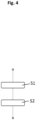
- Steps of a corresponding manufacturing method can follow the flow chart as shown in Figure 4 .
- the housing 2 and the terminals 16 can be formed and/or provided.
- At least one terminal 16 has a given length with respect to the stacking direction A that contributes to a total length larger by at least 0.5 mm than the corresponding length of the side walls 22 of the housing 2.
- a step S2 the terminals 16, the housing 2 and the metal substrate structure 10 are coupled together such that the terminals 16 are arranged inside the housing 2 and coupled to the lower surface 24 of the top wall 21 on the one hand and to the upper surface 14 of the metal top layer 11 on the other hand.
- the terminals 16 provide a compressive load on the metal substrate structure 10 such that it is bent in a predetermined manner and a convex shape of the substrate backside or the bottom surface 15 is formed in interaction with the housing 2 and the terminal 16.
- the terminals 16 can be made from copper or a copper alloy and can realize auxiliary or main terminals.
- a thickness of the terminals 16 can have a value of 0.2 mm up to 3.0 mm with respect to the lateral direction B and/or the stacking direction A. This may apply to both the upright terminal body portion and/or the horizontal terminal foot portion of the L-shaped terminals 16, respectively. Horizontal and vertical sections may have equal or different thicknesses.
- the described embodiments of the semiconductor power module 1 provides an opportunity to form a convex bow of the backside of an insulated metal substrate structure 10 even after the complete module assembly process.
- An improvement of the reliability during module operation can be achieved by exposal of compressive load on the center of the baseplate, so that the convex bow or at least a flat backside remains during long-term operation.
- the semiconductor power module 1 can comprise an integrated structure of module housing 2 and the terminals 16, where the respective terminal feet expose pressure or compressive load on the insulated metal substrate structure 10, so that the pressure provides a convex bow of the backside or bottom surface 15.
- the integrated structure of module housing 2 and the terminals 16 can be realized as one piece or building block forming a terminal or housing block.
- the terminals 16 can be formed as an integral part of such a housing block.
- the housing 2 can be screwed, clamped, or glued to the insulated metal substrate structure 10, so that the design of the housing block allows a compressive load on the metal substrate structure 10.
- the housing 2 is typically fixed to the insulated metal substrate structure 10 by screwed connections. In such a case, corresponding screw holes are available in the insulated metal substrate structure 10 and/or the housing 2. Nevertheless, other methods of mounting are possible like gluing or clamping.
- a sealing material can comprise a rubber sealing or other elastic material.
- the described compressive load on the upper surface 14 of the insulated metal substrate structure 10 can be applied by the terminals 16 by following design options, for example:
- the insulated metal substrate structure 10 can be formed by stamping the metal top layer 11 to have a predetermined metallization pattern, a backside metal sheet and a molded dielectric resin layer 12.
- the insulated metal substrate structure 10 can be formed as a stamped and molded metal substrate, SMMS.
- the metal substrate structure 10 can be formed by laminating and etching of the metal top layer 11.
- the housing 2 can be formed from one piece or two or more separate parts depending on design.
- An integral structure can be prepared by any kind of molding process like transfer or injection molding of resin material embedding at least an upper part of the respective terminal bodies of the terminals 16.
- miscellaneous resin materials like epoxy resin and/or another thermosetting resin, or thermoplastic resin are considerable.
- the resin material may contain any kind of filler like particles or fibers, but also chemical additives e.g. for improved mechanical and/or thermal behavior.
- the connections between the respective terminal feet of the terminals 16 and the upper surface 14 of the insulated metal substrate structure 10 may be realized by miscellaneous joining processes like soldering, ultrasonic welding, laser welding, gluing, and/or sintering or other applicable processes. Also dry contacts are possible.
- the terminals 16 typically consist of copper or copper alloy, which may be coated e.g. by nickel for oxidation prevention.
Landscapes
- Cooling Or The Like Of Semiconductors Or Solid State Devices (AREA)
Claims (15)
- Leistungshalbleitermodul (1), umfassend:- eine Metallsubstratstruktur (10) mit einer oberen Metallschicht (11), einer unteren Metallschicht (13) und einer Dielektrikumsschicht (12), die mit Bezug auf eine Stapelrichtung (A) der Metallsubstratstruktur (10) an sowohl die obere Metallschicht (11) als auch die untere Metallschicht (13) dazwischen gekoppelt ist,- ein Gehäuse (2), das dazu ausgebildet ist, die Elektronik des Leistungshalbleitermoduls (1) zu umschließen, wobei das Gehäuse (2) eine obere Wand (21) und Seitenwände (22) umfasst und an die Metallsubstratstruktur (10) gekoppelt ist, sodass mit Bezug auf die Stapelrichtung (A) jeweils ein vorbestimmter Abstand (D) zwischen einer Unterseitenfläche (24) der oberen Wand (21) und einer Oberseitenfläche (14) der oberen Metallschicht (11) neben den Seitenwänden (22) gegeben ist, und- mindestens einen innerhalb des Gehäuses (2) angeordneten Anschluss (16), wobei der mindestens eine Anschluss (16) einerseits an die Unterseitenfläche (24) der oberen Wand (21) gekoppelt ist und andererseits an die Oberseitenfläche (14) der oberen Metallschicht (11) gekoppelt ist und wobei mit Bezug auf die Stapelrichtung (A) eine Länge mindestens eines Anschlusses (16) in Abstimmung mit dem Abstand (D) ausgebildet ist, sodass aufgrund des mindestens einen Anschlusses (16) die Metallsubstratstruktur (10) auf eine vorbestimmte Weise gebogen wird und eine konvexe Form in Wechselwirkung mit dem Gehäuse (2) umfasst.
- Leistungshalbleitermodul (1) nach Anspruch 1, wobei eine Gesamtlänge, die die Länge des mindestens einen Anschlusses (16) beinhaltet, vorgegeben ist, sodass in der Richtung zu der oberen Metallschicht (11) hin der mindestens eine Anschluss (16) über die Länge der Seitenwände (22) hinaus um mindestens 0,5 mm vorsteht.
- Leistungshalbleitermodul (1) nach einem der vorhergehenden Ansprüche, wobei das Gehäuse (2) und die Metallsubstratstruktur (10) durch Verschrauben und/oder Kleben und/oder Klemmen und/oder Abdichten aneinander gekoppelt sind.
- Leistungshalbleitermodul (1) nach Anspruch 3, wobei das Gehäuse und/oder die untere Metallschicht (13) ein jeweiliges Schraubloch oder jeweilige mehrere Schraublöcher umfassen/umfasst und das Gehäuse (2) und die Metallsubstratstruktur (10) durch Schraubverbindungen aneinander gekoppelt sind, wobei die Schraubverbindungen in einem jeweiligen Bereich neben den Seitenwänden (22) des Gehäuses (2) positioniert sind.
- Leistungshalbleitermodul (1) nach einem der vorhergehenden Ansprüche, wobei das Gehäuse (2) durch Formen gebildet ist und wobei der mindestens eine Anschluss (16) teilweise eingebettet in dem geformten Gehäuse (2) integral an die obere Wand (21) gekoppelt ist.
- Leistungshalbleitermodul (1) nach einem der vorhergehenden Ansprüche, wobei der mindestens eine Anschluss (16) mit der Unterseitenfläche (24) der oberen Wand (21) und/oder mit der Oberseitenfläche (14) der oberen Metallschicht (11) durch Klemmen und/oder Löten und/oder Schweißen und/oder Kleben und/oder Sintern verbunden ist.
- Leistungshalbleitermodul (1) nach einem der vorhergehenden Ansprüche, umfassend:
zwei oder mehr Anschlüsse (16), die innerhalb des Gehäuses (2) angeordnet und einerseits mit der Unterseitenfläche (24) der oberen Wand (21) und andererseits mit der Oberseitenfläche (14) der oberen Metallschicht (11) gekoppelt sind, wobei die zwei oder mehr Anschlüsse (16) unterschiedliche Längen mit Bezug auf die Stapelrichtung (A) zwischen der Unterseitenfläche (24) und der Oberseitenfläche (14) umfassen. - Leistungshalbleitermodul (1) nach Anspruch 7, wobei die zwei oder mehr Anschlüsse (16) mit Bezug auf eine Mittelachse (M) oder eine Symmetrieebene symmetrisch innerhalb des Gehäuses (2) entlang einer senkrecht zu der Stapelrichtung (A) verlaufenden Querrichtung (B) angeordnet sind.
- Leistungshalbleitermodul (1) nach einem der vorhergehenden Ansprüche, wobei der mindestens eine Anschluss (16) eine Feder oder ein Gummiband oder eine Spannungsentlastungsstruktur umfasst, die/das dazu ausgebildet ist, die Metallsubstratstruktur (10) auf eine vorbestimmte Weise mit Druck zu beaufschlagen.
- Leistungshalbleitermodul (1) nach einem der vorhergehenden Ansprüche, umfassend:
ein Polsterelement, das an den mindestens einen Anschluss (16) gekoppelt und dazu ausgebildet ist, den Anschluss und/oder die Metallsubstratstruktur (10) auf eine vorbestimmte Weise mit Druck zu beaufschlagen. - Leistungshalbleitermodul (1) nach einem der vorhergehenden Ansprüche, wobei der mindestens eine Anschluss (16) einen langgestreckten Anschlusskörper und einen plattenförmigen Anschlussfuß mit einer Kontaktoberfläche (17) umfasst, die mit der Oberseitenfläche (14) der Metallsubstratstruktur (10) in Kontakt steht oder ihr zugewandt ist.
- Leistungshalbleitermodul (1) nach Anspruch 11, wobei die Kontaktoberfläche (17) des Anschlussfußes und/oder ein Kontaktabschnitt der Oberseitenfläche (14) der oberen Metallschicht (11) mit einem Überzug, der mindestens eine Schicht aus Gold und/oder Silber und/oder Nickel umfasst, beschichtet sind/ist.
- Leistungshalbleitermodul (1) nach einem der vorhergehenden Ansprüche, umfassend:
einen Kühlkörper (3), der an eine untere Oberfläche (15) der unteren Metallschicht (13) gekoppelt ist. - Verfahren zum Herstellen eines Leistungshalbleitermoduls (1), umfassend:- Bereitstellen einer Metallsubstratstruktur (10) mit einer oberen Metallschicht (11), einer unteren Metallschicht (13) und einer Dielektrikumsschicht (12), die mit Bezug auf eine Stapelrichtung (A) der Metallsubstratstruktur (10) an sowohl die obere Metallschicht (11) als auch die untere Metallschicht (13) dazwischen gekoppelt ist,- Bereitstellen eines Gehäuses (2) mit einer oberen Wand (21) und Seitenwänden (22) mit vorgegebenen Längen,- Bereitstellen mindestens eines Anschlusses (16) mit einer vorgegebenen Länge und- Zusammenkoppeln des mindestens einen Anschlusses (16), des Gehäuses (2) und der Metallsubstratstruktur (10), sodass der mindestens eine Anschluss (16) innerhalb des Gehäuses (2) angeordnet und einerseits mit einer Unterseitenfläche (24) der oberen Wand (21) gekoppelt ist und andererseits mit einer Oberseitenfläche (14) der oberen Metallschicht (11) gekoppelt ist, wobei die Länge mindestens eines Anschlusses (16) jeweils in Abstimmung mit einem Abstand (D) zwischen der Unterseitenfläche (24) der oberen Wand (21) und der Oberseitenfläche (14) der oberen Metallschicht (11) neben den Seitenwänden (22) ausgebildet ist, und dadurch Bereitstellen einer Drucklast auf der Metallsubstratstruktur (10) aufgrund des mindestens einen Anschlusses (16), sodass die Metallsubstratstruktur (10) auf eine vorbestimmte Weise gebogen wird und eine konvexe Form in Wechselwirkung mit dem Gehäuse (2) und dem mindestens einen Anschluss (16) umfasst.
- Verfahren nach Anspruch 14, wobei der Schritt des Zusammenkoppelns des mindestens einen Anschlusses (16), des Gehäuses (2) und der Metallsubstratstruktur (10) Folgendes umfasst:- Bilden des Gehäuses (2) durch Formen, sodass der mindestens eine Anschluss (16) teilweise eingebettet in dem geformten Gehäuse (2) integral an die obere Wand (21) gekoppelt ist, und- Koppeln des geformten Gehäuses (2) und des mindestens einen eingebetteten Anschlusses (16) an die Metallsubstratstruktur (10) durch Verschrauben und/oder Klemmen und/oder Kleben und/oder Abdichten.
Applications Claiming Priority (1)
| Application Number | Priority Date | Filing Date | Title |
|---|---|---|---|
| PCT/EP2022/061344 WO2023208348A1 (en) | 2022-04-28 | 2022-04-28 | Semiconductor power module and method for manufacturing a semiconductor power module |
Publications (2)
| Publication Number | Publication Date |
|---|---|
| EP4292129A1 EP4292129A1 (de) | 2023-12-20 |
| EP4292129B1 true EP4292129B1 (de) | 2024-06-26 |
Family
ID=88532299
Family Applications (1)
| Application Number | Title | Priority Date | Filing Date |
|---|---|---|---|
| EP22726412.4A Active EP4292129B1 (de) | 2022-04-28 | 2022-04-28 | Leistungshalbleitermodul und verfahren zur herstellung eines leistungshalbleitermoduls |
Country Status (5)
| Country | Link |
|---|---|
| US (1) | US20240063080A1 (de) |
| EP (1) | EP4292129B1 (de) |
| JP (1) | JP7811580B2 (de) |
| CN (1) | CN117321762B (de) |
| WO (1) | WO2023208348A1 (de) |
Family Cites Families (26)
| Publication number | Priority date | Publication date | Assignee | Title |
|---|---|---|---|---|
| DE4001554A1 (de) * | 1990-01-20 | 1991-07-25 | Abb Ixys Semiconductor Gmbh | Leistungshalbleitermodul |
| JP2913247B2 (ja) * | 1993-08-11 | 1999-06-28 | 株式会社日立製作所 | パワー半導体モジュール及び車両用インバータ装置 |
| JPH08204071A (ja) * | 1995-01-27 | 1996-08-09 | Toshiba Corp | 半導体装置 |
| DE19615481C5 (de) * | 1996-04-03 | 2013-03-14 | Curamik Electronics Gmbh | Gewölbtes Metall-Keramik-Substrat |
| JP3448159B2 (ja) * | 1996-06-20 | 2003-09-16 | 株式会社東芝 | 電力用半導体装置 |
| DE10326176A1 (de) * | 2003-06-10 | 2005-01-05 | eupec Europäische Gesellschaft für Leistungshalbleiter mbH | Leistungshalbleitermodul |
| DE10333329B4 (de) * | 2003-07-23 | 2011-07-21 | SEMIKRON Elektronik GmbH & Co. KG, 90431 | Leistungshalbleitermodul mit biegesteifer Grundplatte |
| DE102004043019A1 (de) * | 2004-09-06 | 2006-03-23 | eupec Europäische Gesellschaft für Leistungshalbleiter mbH | Baugruppe |
| US7453139B2 (en) * | 2005-12-27 | 2008-11-18 | Tessera, Inc. | Compliant terminal mountings with vented spaces and methods |
| US7511961B2 (en) * | 2006-10-26 | 2009-03-31 | Infineon Technologies Ag | Base plate for a power semiconductor module |
| US8154114B2 (en) * | 2007-08-06 | 2012-04-10 | Infineon Technologies Ag | Power semiconductor module |
| US7808100B2 (en) * | 2008-04-21 | 2010-10-05 | Infineon Technologies Ag | Power semiconductor module with pressure element and method for fabricating a power semiconductor module with a pressure element |
| US7919854B2 (en) * | 2008-08-15 | 2011-04-05 | Infineon Technologies Ag | Semiconductor module with two cooling surfaces and method |
| DE102008048005B3 (de) * | 2008-09-19 | 2010-04-08 | Infineon Technologies Ag | Leistungshalbleitermodulanordnung und Verfahren zur Herstellung einer Leistungshalbleitermodulanordnung |
| JP2010212620A (ja) | 2009-03-12 | 2010-09-24 | Toshiba Corp | パワーモジュール |
| CN104701277B (zh) * | 2013-12-10 | 2017-12-05 | 江苏宏微科技股份有限公司 | 功率模块的封装结构 |
| CN106298689B (zh) * | 2015-05-28 | 2018-10-09 | 台达电子企业管理(上海)有限公司 | 封装结构 |
| DE102015221062B4 (de) * | 2015-10-28 | 2020-04-23 | Vincotech Gmbh | Halbleiterschaltungsanordnung mit gepresstem gel und montageverfahren |
| JP2018022757A (ja) | 2016-08-03 | 2018-02-08 | 富士電機株式会社 | 半導体モジュール |
| JP6897056B2 (ja) | 2016-10-20 | 2021-06-30 | 富士電機株式会社 | 半導体装置及び半導体装置製造方法 |
| EP3340291B1 (de) * | 2016-12-23 | 2024-10-30 | Infineon Technologies AG | Verfahren zur herstellung einer elektronischen modulanordnung und elektronische modulanordnung |
| JP6421859B2 (ja) | 2017-10-10 | 2018-11-14 | 三菱電機株式会社 | 半導体装置 |
| EP3518278A1 (de) * | 2018-01-30 | 2019-07-31 | Infineon Technologies AG | Leistungshalbleitermodul und verfahren zur dessen herstellung |
| DE202018100486U1 (de) * | 2018-01-30 | 2018-02-22 | Infineon Technologies Ag | Leistungshalbleitermodul |
| JP7562953B2 (ja) * | 2020-02-14 | 2024-10-08 | 富士電機株式会社 | 半導体モジュール |
| EP3872854A1 (de) * | 2020-02-27 | 2021-09-01 | Littelfuse, Inc. | Leistungsmodulgehäuse mit verbessertem vorsprungsdesign |
-
2022
- 2022-04-28 JP JP2023519815A patent/JP7811580B2/ja active Active
- 2022-04-28 CN CN202280006662.2A patent/CN117321762B/zh active Active
- 2022-04-28 US US18/029,020 patent/US20240063080A1/en active Pending
- 2022-04-28 WO PCT/EP2022/061344 patent/WO2023208348A1/en not_active Ceased
- 2022-04-28 EP EP22726412.4A patent/EP4292129B1/de active Active
Also Published As
| Publication number | Publication date |
|---|---|
| JP7811580B2 (ja) | 2026-02-05 |
| CN117321762B (zh) | 2026-03-20 |
| US20240063080A1 (en) | 2024-02-22 |
| CN117321762A (zh) | 2023-12-29 |
| WO2023208348A1 (en) | 2023-11-02 |
| JP2025512142A (ja) | 2025-04-17 |
| EP4292129A1 (de) | 2023-12-20 |
Similar Documents
| Publication | Publication Date | Title |
|---|---|---|
| KR100563122B1 (ko) | 하이브리드 모듈 및 그 제조방법 및 그 설치방법 | |
| JP4825259B2 (ja) | 電力用半導体モジュール及びその製造方法 | |
| JP3605547B2 (ja) | 放熱基板及びその製造方法 | |
| CN106211712A (zh) | 控制装置 | |
| US12500152B2 (en) | Power semiconductor module, method for assembling a power semiconductor module and housing for a power semiconductor module | |
| US12512388B2 (en) | Semiconductor device and method of manufacturing semiconductor device | |
| EP3913665B1 (de) | Leistungshalbleitermodul und verfahren zur herstellung eines leistungshalbleitermoduls | |
| EP2804209A1 (de) | Geformtes Elektronikmodul | |
| US20240222208A1 (en) | Power electronic module, power electronic module block, printed circuit board with power electronic module or printed circuit board component,and method for producing a power electronic module | |
| EP1610381B1 (de) | Elektronikgehäuse mit segmentierten Verbindungen und Lotverbindung | |
| JP2004363183A (ja) | 電子部品の放熱構造 | |
| EP4292129B1 (de) | Leistungshalbleitermodul und verfahren zur herstellung eines leistungshalbleitermoduls | |
| US12218192B2 (en) | Metal substrate structure for a semiconductor power module | |
| CN119110984B (zh) | 将端子附接到半导体功率模块的绝缘金属基部结构的方法以及半导体功率模块 | |
| JP7660708B2 (ja) | 半導体パワーモジュール、ならびに半導体パワーモジュールおよび半導体パワーデバイスを製造するための方法 | |
| JP7675197B2 (ja) | 金属基板構造体、半導体パワーモジュール用の金属基板構造体の製造方法、および半導体パワーモジュール | |
| JP2024540770A (ja) | 電子部品及び電子部品を製造するための方法 | |
| EP4239660A1 (de) | Verfahren zum befestigen eines anschlusses an einer metallsubstratstruktur für ein halbleiterleistungsmodul und halbleiterleistungsmodul | |
| EP4057338B1 (de) | Metallsubstratstruktur und verfahren zur herstellung einer metallsubstratstruktur für ein halbleiterleistungsmodul sowie halbleiterleistungsmodul | |
| WO2023152343A1 (en) | Molded power module and power module assembly | |
| CN121693134A (zh) | 具有散热结构的电子部件 |
Legal Events
| Date | Code | Title | Description |
|---|---|---|---|
| STAA | Information on the status of an ep patent application or granted ep patent |
Free format text: STATUS: UNKNOWN |
|
| STAA | Information on the status of an ep patent application or granted ep patent |
Free format text: STATUS: THE INTERNATIONAL PUBLICATION HAS BEEN MADE |
|
| PUAI | Public reference made under article 153(3) epc to a published international application that has entered the european phase |
Free format text: ORIGINAL CODE: 0009012 |
|
| STAA | Information on the status of an ep patent application or granted ep patent |
Free format text: STATUS: REQUEST FOR EXAMINATION WAS MADE |
|
| 17P | Request for examination filed |
Effective date: 20230221 |
|
| AK | Designated contracting states |
Kind code of ref document: A1 Designated state(s): AL AT BE BG CH CY CZ DE DK EE ES FI FR GB GR HR HU IE IS IT LI LT LU LV MC MK MT NL NO PL PT RO RS SE SI SK SM TR |
|
| REG | Reference to a national code |
Ref country code: DE Free format text: PREVIOUS MAIN CLASS: H01L0025070000 Ref country code: DE Ref legal event code: R079 Ref document number: 602022004190 Country of ref document: DE Free format text: PREVIOUS MAIN CLASS: H01L0025070000 Ipc: H01L0023367000 |
|
| GRAP | Despatch of communication of intention to grant a patent |
Free format text: ORIGINAL CODE: EPIDOSNIGR1 |
|
| STAA | Information on the status of an ep patent application or granted ep patent |
Free format text: STATUS: GRANT OF PATENT IS INTENDED |
|
| RIC1 | Information provided on ipc code assigned before grant |
Ipc: H01L 23/367 20060101AFI20240201BHEP |
|
| DAV | Request for validation of the european patent (deleted) | ||
| DAX | Request for extension of the european patent (deleted) | ||
| INTG | Intention to grant announced |
Effective date: 20240222 |
|
| P01 | Opt-out of the competence of the unified patent court (upc) registered |
Effective date: 20240408 |
|
| GRAS | Grant fee paid |
Free format text: ORIGINAL CODE: EPIDOSNIGR3 |
|
| GRAA | (expected) grant |
Free format text: ORIGINAL CODE: 0009210 |
|
| STAA | Information on the status of an ep patent application or granted ep patent |
Free format text: STATUS: THE PATENT HAS BEEN GRANTED |
|
| AK | Designated contracting states |
Kind code of ref document: B1 Designated state(s): AL AT BE BG CH CY CZ DE DK EE ES FI FR GB GR HR HU IE IS IT LI LT LU LV MC MK MT NL NO PL PT RO RS SE SI SK SM TR |
|
| REG | Reference to a national code |
Ref country code: GB Ref legal event code: FG4D |
|
| REG | Reference to a national code |
Ref country code: CH Ref legal event code: EP |
|
| REG | Reference to a national code |
Ref country code: DE Ref legal event code: R096 Ref document number: 602022004190 Country of ref document: DE |
|
| PG25 | Lapsed in a contracting state [announced via postgrant information from national office to epo] |
Ref country code: BG Free format text: LAPSE BECAUSE OF FAILURE TO SUBMIT A TRANSLATION OF THE DESCRIPTION OR TO PAY THE FEE WITHIN THE PRESCRIBED TIME-LIMIT Effective date: 20240626 |
|
| PG25 | Lapsed in a contracting state [announced via postgrant information from national office to epo] |
Ref country code: FI Free format text: LAPSE BECAUSE OF FAILURE TO SUBMIT A TRANSLATION OF THE DESCRIPTION OR TO PAY THE FEE WITHIN THE PRESCRIBED TIME-LIMIT Effective date: 20240626 Ref country code: HR Free format text: LAPSE BECAUSE OF FAILURE TO SUBMIT A TRANSLATION OF THE DESCRIPTION OR TO PAY THE FEE WITHIN THE PRESCRIBED TIME-LIMIT Effective date: 20240626 |
|
| REG | Reference to a national code |
Ref country code: LT Ref legal event code: MG9D |
|
| PG25 | Lapsed in a contracting state [announced via postgrant information from national office to epo] |
Ref country code: GR Free format text: LAPSE BECAUSE OF FAILURE TO SUBMIT A TRANSLATION OF THE DESCRIPTION OR TO PAY THE FEE WITHIN THE PRESCRIBED TIME-LIMIT Effective date: 20240927 |
|
| PG25 | Lapsed in a contracting state [announced via postgrant information from national office to epo] |
Ref country code: LV Free format text: LAPSE BECAUSE OF FAILURE TO SUBMIT A TRANSLATION OF THE DESCRIPTION OR TO PAY THE FEE WITHIN THE PRESCRIBED TIME-LIMIT Effective date: 20240626 |
|
| REG | Reference to a national code |
Ref country code: NL Ref legal event code: MP Effective date: 20240626 |
|
| PG25 | Lapsed in a contracting state [announced via postgrant information from national office to epo] |
Ref country code: NO Free format text: LAPSE BECAUSE OF FAILURE TO SUBMIT A TRANSLATION OF THE DESCRIPTION OR TO PAY THE FEE WITHIN THE PRESCRIBED TIME-LIMIT Effective date: 20240926 Ref country code: LV Free format text: LAPSE BECAUSE OF FAILURE TO SUBMIT A TRANSLATION OF THE DESCRIPTION OR TO PAY THE FEE WITHIN THE PRESCRIBED TIME-LIMIT Effective date: 20240626 Ref country code: HR Free format text: LAPSE BECAUSE OF FAILURE TO SUBMIT A TRANSLATION OF THE DESCRIPTION OR TO PAY THE FEE WITHIN THE PRESCRIBED TIME-LIMIT Effective date: 20240626 Ref country code: GR Free format text: LAPSE BECAUSE OF FAILURE TO SUBMIT A TRANSLATION OF THE DESCRIPTION OR TO PAY THE FEE WITHIN THE PRESCRIBED TIME-LIMIT Effective date: 20240927 Ref country code: FI Free format text: LAPSE BECAUSE OF FAILURE TO SUBMIT A TRANSLATION OF THE DESCRIPTION OR TO PAY THE FEE WITHIN THE PRESCRIBED TIME-LIMIT Effective date: 20240626 Ref country code: BG Free format text: LAPSE BECAUSE OF FAILURE TO SUBMIT A TRANSLATION OF THE DESCRIPTION OR TO PAY THE FEE WITHIN THE PRESCRIBED TIME-LIMIT Effective date: 20240626 Ref country code: RS Free format text: LAPSE BECAUSE OF FAILURE TO SUBMIT A TRANSLATION OF THE DESCRIPTION OR TO PAY THE FEE WITHIN THE PRESCRIBED TIME-LIMIT Effective date: 20240926 |
|
| PG25 | Lapsed in a contracting state [announced via postgrant information from national office to epo] |
Ref country code: NL Free format text: LAPSE BECAUSE OF FAILURE TO SUBMIT A TRANSLATION OF THE DESCRIPTION OR TO PAY THE FEE WITHIN THE PRESCRIBED TIME-LIMIT Effective date: 20240626 |
|
| REG | Reference to a national code |
Ref country code: AT Ref legal event code: MK05 Ref document number: 1698439 Country of ref document: AT Kind code of ref document: T Effective date: 20240626 |
|
| PG25 | Lapsed in a contracting state [announced via postgrant information from national office to epo] |
Ref country code: NL Free format text: LAPSE BECAUSE OF FAILURE TO SUBMIT A TRANSLATION OF THE DESCRIPTION OR TO PAY THE FEE WITHIN THE PRESCRIBED TIME-LIMIT Effective date: 20240626 |
|
| PG25 | Lapsed in a contracting state [announced via postgrant information from national office to epo] |
Ref country code: PT Free format text: LAPSE BECAUSE OF FAILURE TO SUBMIT A TRANSLATION OF THE DESCRIPTION OR TO PAY THE FEE WITHIN THE PRESCRIBED TIME-LIMIT Effective date: 20241028 |
|
| PG25 | Lapsed in a contracting state [announced via postgrant information from national office to epo] |
Ref country code: PT Free format text: LAPSE BECAUSE OF FAILURE TO SUBMIT A TRANSLATION OF THE DESCRIPTION OR TO PAY THE FEE WITHIN THE PRESCRIBED TIME-LIMIT Effective date: 20241028 |
|
| PG25 | Lapsed in a contracting state [announced via postgrant information from national office to epo] |
Ref country code: PL Free format text: LAPSE BECAUSE OF FAILURE TO SUBMIT A TRANSLATION OF THE DESCRIPTION OR TO PAY THE FEE WITHIN THE PRESCRIBED TIME-LIMIT Effective date: 20240626 |
|
| PG25 | Lapsed in a contracting state [announced via postgrant information from national office to epo] |
Ref country code: EE Free format text: LAPSE BECAUSE OF FAILURE TO SUBMIT A TRANSLATION OF THE DESCRIPTION OR TO PAY THE FEE WITHIN THE PRESCRIBED TIME-LIMIT Effective date: 20240626 |
|
| PG25 | Lapsed in a contracting state [announced via postgrant information from national office to epo] |
Ref country code: IS Free format text: LAPSE BECAUSE OF FAILURE TO SUBMIT A TRANSLATION OF THE DESCRIPTION OR TO PAY THE FEE WITHIN THE PRESCRIBED TIME-LIMIT Effective date: 20241026 Ref country code: AT Free format text: LAPSE BECAUSE OF FAILURE TO SUBMIT A TRANSLATION OF THE DESCRIPTION OR TO PAY THE FEE WITHIN THE PRESCRIBED TIME-LIMIT Effective date: 20240626 |
|
| PG25 | Lapsed in a contracting state [announced via postgrant information from national office to epo] |
Ref country code: CZ Free format text: LAPSE BECAUSE OF FAILURE TO SUBMIT A TRANSLATION OF THE DESCRIPTION OR TO PAY THE FEE WITHIN THE PRESCRIBED TIME-LIMIT Effective date: 20240626 |
|
| PG25 | Lapsed in a contracting state [announced via postgrant information from national office to epo] |
Ref country code: SK Free format text: LAPSE BECAUSE OF FAILURE TO SUBMIT A TRANSLATION OF THE DESCRIPTION OR TO PAY THE FEE WITHIN THE PRESCRIBED TIME-LIMIT Effective date: 20240626 Ref country code: RO Free format text: LAPSE BECAUSE OF FAILURE TO SUBMIT A TRANSLATION OF THE DESCRIPTION OR TO PAY THE FEE WITHIN THE PRESCRIBED TIME-LIMIT Effective date: 20240626 |
|
| PG25 | Lapsed in a contracting state [announced via postgrant information from national office to epo] |
Ref country code: SM Free format text: LAPSE BECAUSE OF FAILURE TO SUBMIT A TRANSLATION OF THE DESCRIPTION OR TO PAY THE FEE WITHIN THE PRESCRIBED TIME-LIMIT Effective date: 20240626 Ref country code: ES Free format text: LAPSE BECAUSE OF FAILURE TO SUBMIT A TRANSLATION OF THE DESCRIPTION OR TO PAY THE FEE WITHIN THE PRESCRIBED TIME-LIMIT Effective date: 20240626 |
|
| PG25 | Lapsed in a contracting state [announced via postgrant information from national office to epo] |
Ref country code: SM Free format text: LAPSE BECAUSE OF FAILURE TO SUBMIT A TRANSLATION OF THE DESCRIPTION OR TO PAY THE FEE WITHIN THE PRESCRIBED TIME-LIMIT Effective date: 20240626 Ref country code: SK Free format text: LAPSE BECAUSE OF FAILURE TO SUBMIT A TRANSLATION OF THE DESCRIPTION OR TO PAY THE FEE WITHIN THE PRESCRIBED TIME-LIMIT Effective date: 20240626 Ref country code: RO Free format text: LAPSE BECAUSE OF FAILURE TO SUBMIT A TRANSLATION OF THE DESCRIPTION OR TO PAY THE FEE WITHIN THE PRESCRIBED TIME-LIMIT Effective date: 20240626 Ref country code: PL Free format text: LAPSE BECAUSE OF FAILURE TO SUBMIT A TRANSLATION OF THE DESCRIPTION OR TO PAY THE FEE WITHIN THE PRESCRIBED TIME-LIMIT Effective date: 20240626 Ref country code: IS Free format text: LAPSE BECAUSE OF FAILURE TO SUBMIT A TRANSLATION OF THE DESCRIPTION OR TO PAY THE FEE WITHIN THE PRESCRIBED TIME-LIMIT Effective date: 20241026 Ref country code: ES Free format text: LAPSE BECAUSE OF FAILURE TO SUBMIT A TRANSLATION OF THE DESCRIPTION OR TO PAY THE FEE WITHIN THE PRESCRIBED TIME-LIMIT Effective date: 20240626 Ref country code: EE Free format text: LAPSE BECAUSE OF FAILURE TO SUBMIT A TRANSLATION OF THE DESCRIPTION OR TO PAY THE FEE WITHIN THE PRESCRIBED TIME-LIMIT Effective date: 20240626 Ref country code: CZ Free format text: LAPSE BECAUSE OF FAILURE TO SUBMIT A TRANSLATION OF THE DESCRIPTION OR TO PAY THE FEE WITHIN THE PRESCRIBED TIME-LIMIT Effective date: 20240626 Ref country code: AT Free format text: LAPSE BECAUSE OF FAILURE TO SUBMIT A TRANSLATION OF THE DESCRIPTION OR TO PAY THE FEE WITHIN THE PRESCRIBED TIME-LIMIT Effective date: 20240626 |
|
| PG25 | Lapsed in a contracting state [announced via postgrant information from national office to epo] |
Ref country code: IT Free format text: LAPSE BECAUSE OF FAILURE TO SUBMIT A TRANSLATION OF THE DESCRIPTION OR TO PAY THE FEE WITHIN THE PRESCRIBED TIME-LIMIT Effective date: 20240626 |
|
| REG | Reference to a national code |
Ref country code: DE Ref legal event code: R097 Ref document number: 602022004190 Country of ref document: DE |
|
| PG25 | Lapsed in a contracting state [announced via postgrant information from national office to epo] |
Ref country code: DK Free format text: LAPSE BECAUSE OF FAILURE TO SUBMIT A TRANSLATION OF THE DESCRIPTION OR TO PAY THE FEE WITHIN THE PRESCRIBED TIME-LIMIT Effective date: 20240626 |
|
| PLBE | No opposition filed within time limit |
Free format text: ORIGINAL CODE: 0009261 |
|
| STAA | Information on the status of an ep patent application or granted ep patent |
Free format text: STATUS: NO OPPOSITION FILED WITHIN TIME LIMIT |
|
| 26N | No opposition filed |
Effective date: 20250327 |
|
| PGFP | Annual fee paid to national office [announced via postgrant information from national office to epo] |
Ref country code: DE Payment date: 20250422 Year of fee payment: 4 |
|
| PG25 | Lapsed in a contracting state [announced via postgrant information from national office to epo] |
Ref country code: SE Free format text: LAPSE BECAUSE OF FAILURE TO SUBMIT A TRANSLATION OF THE DESCRIPTION OR TO PAY THE FEE WITHIN THE PRESCRIBED TIME-LIMIT Effective date: 20240626 |
|
| REG | Reference to a national code |
Ref country code: CH Ref legal event code: H13 Free format text: ST27 STATUS EVENT CODE: U-0-0-H10-H13 (AS PROVIDED BY THE NATIONAL OFFICE) Effective date: 20251125 |
|
| REG | Reference to a national code |
Ref country code: DE Ref legal event code: R079 Ref document number: 602022004190 Country of ref document: DE Free format text: PREVIOUS MAIN CLASS: H01L0023367000 Ipc: H10W0040220000 |
|
| PG25 | Lapsed in a contracting state [announced via postgrant information from national office to epo] |
Ref country code: LU Free format text: LAPSE BECAUSE OF NON-PAYMENT OF DUE FEES Effective date: 20250428 |
|
| PG25 | Lapsed in a contracting state [announced via postgrant information from national office to epo] |
Ref country code: MC Free format text: LAPSE BECAUSE OF FAILURE TO SUBMIT A TRANSLATION OF THE DESCRIPTION OR TO PAY THE FEE WITHIN THE PRESCRIBED TIME-LIMIT Effective date: 20240626 |
|
| REG | Reference to a national code |
Ref country code: BE Ref legal event code: MM Effective date: 20250430 |
|
| PG25 | Lapsed in a contracting state [announced via postgrant information from national office to epo] |
Ref country code: FR Free format text: LAPSE BECAUSE OF NON-PAYMENT OF DUE FEES Effective date: 20250430 |
|
| PG25 | Lapsed in a contracting state [announced via postgrant information from national office to epo] |
Ref country code: BE Free format text: LAPSE BECAUSE OF NON-PAYMENT OF DUE FEES Effective date: 20250430 |
|
| PG25 | Lapsed in a contracting state [announced via postgrant information from national office to epo] |
Ref country code: CH Free format text: LAPSE BECAUSE OF NON-PAYMENT OF DUE FEES Effective date: 20250430 |
|
| PG25 | Lapsed in a contracting state [announced via postgrant information from national office to epo] |
Ref country code: IE Free format text: LAPSE BECAUSE OF NON-PAYMENT OF DUE FEES Effective date: 20250428 |