EP4287784A1 - Mikrowellenplasmabehandlungsvorrichtung - Google Patents
Mikrowellenplasmabehandlungsvorrichtung Download PDFInfo
- Publication number
- EP4287784A1 EP4287784A1 EP22745881.7A EP22745881A EP4287784A1 EP 4287784 A1 EP4287784 A1 EP 4287784A1 EP 22745881 A EP22745881 A EP 22745881A EP 4287784 A1 EP4287784 A1 EP 4287784A1
- Authority
- EP
- European Patent Office
- Prior art keywords
- microwave
- resonator
- phase
- container
- treatment device
- Prior art date
- Legal status (The legal status is an assumption and is not a legal conclusion. Google has not performed a legal analysis and makes no representation as to the accuracy of the status listed.)
- Pending
Links
- 238000009832 plasma treatment Methods 0.000 title claims abstract description 56
- 230000007246 mechanism Effects 0.000 claims abstract description 41
- 230000010355 oscillation Effects 0.000 claims abstract description 23
- 239000010432 diamond Substances 0.000 description 24
- 229910003460 diamond Inorganic materials 0.000 description 24
- 239000000758 substrate Substances 0.000 description 19
- 239000007789 gas Substances 0.000 description 11
- 238000010586 diagram Methods 0.000 description 9
- 230000015572 biosynthetic process Effects 0.000 description 7
- 238000004519 manufacturing process Methods 0.000 description 7
- 238000004088 simulation Methods 0.000 description 6
- 239000000470 constituent Substances 0.000 description 4
- 239000013078 crystal Substances 0.000 description 4
- 230000000694 effects Effects 0.000 description 4
- 230000005684 electric field Effects 0.000 description 4
- 239000000463 material Substances 0.000 description 4
- 238000005229 chemical vapour deposition Methods 0.000 description 3
- IJGRMHOSHXDMSA-UHFFFAOYSA-N Atomic nitrogen Chemical compound N#N IJGRMHOSHXDMSA-UHFFFAOYSA-N 0.000 description 2
- OKTJSMMVPCPJKN-UHFFFAOYSA-N Carbon Chemical compound [C] OKTJSMMVPCPJKN-UHFFFAOYSA-N 0.000 description 2
- PXHVJJICTQNCMI-UHFFFAOYSA-N Nickel Chemical compound [Ni] PXHVJJICTQNCMI-UHFFFAOYSA-N 0.000 description 2
- 229910052799 carbon Inorganic materials 0.000 description 2
- BASFCYQUMIYNBI-UHFFFAOYSA-N platinum Chemical compound [Pt] BASFCYQUMIYNBI-UHFFFAOYSA-N 0.000 description 2
- 229910002601 GaN Inorganic materials 0.000 description 1
- JMASRVWKEDWRBT-UHFFFAOYSA-N Gallium nitride Chemical compound [Ga]#N JMASRVWKEDWRBT-UHFFFAOYSA-N 0.000 description 1
- ZOKXTWBITQBERF-UHFFFAOYSA-N Molybdenum Chemical compound [Mo] ZOKXTWBITQBERF-UHFFFAOYSA-N 0.000 description 1
- VYPSYNLAJGMNEJ-UHFFFAOYSA-N Silicium dioxide Chemical compound O=[Si]=O VYPSYNLAJGMNEJ-UHFFFAOYSA-N 0.000 description 1
- PNEYBMLMFCGWSK-UHFFFAOYSA-N aluminium oxide Inorganic materials [O-2].[O-2].[O-2].[Al+3].[Al+3] PNEYBMLMFCGWSK-UHFFFAOYSA-N 0.000 description 1
- QVGXLLKOCUKJST-UHFFFAOYSA-N atomic oxygen Chemical compound [O] QVGXLLKOCUKJST-UHFFFAOYSA-N 0.000 description 1
- 230000005540 biological transmission Effects 0.000 description 1
- 230000007423 decrease Effects 0.000 description 1
- AJNVQOSZGJRYEI-UHFFFAOYSA-N digallium;oxygen(2-) Chemical compound [O-2].[O-2].[O-2].[Ga+3].[Ga+3] AJNVQOSZGJRYEI-UHFFFAOYSA-N 0.000 description 1
- 238000009826 distribution Methods 0.000 description 1
- 229910001195 gallium oxide Inorganic materials 0.000 description 1
- 239000001257 hydrogen Substances 0.000 description 1
- 229910052739 hydrogen Inorganic materials 0.000 description 1
- 125000004435 hydrogen atom Chemical class [H]* 0.000 description 1
- 150000002500 ions Chemical class 0.000 description 1
- 229910052741 iridium Inorganic materials 0.000 description 1
- GKOZUEZYRPOHIO-UHFFFAOYSA-N iridium atom Chemical compound [Ir] GKOZUEZYRPOHIO-UHFFFAOYSA-N 0.000 description 1
- CPLXHLVBOLITMK-UHFFFAOYSA-N magnesium oxide Inorganic materials [Mg]=O CPLXHLVBOLITMK-UHFFFAOYSA-N 0.000 description 1
- 239000000395 magnesium oxide Substances 0.000 description 1
- AXZKOIWUVFPNLO-UHFFFAOYSA-N magnesium;oxygen(2-) Chemical compound [O-2].[Mg+2] AXZKOIWUVFPNLO-UHFFFAOYSA-N 0.000 description 1
- 230000008018 melting Effects 0.000 description 1
- 238000002844 melting Methods 0.000 description 1
- 229910052751 metal Inorganic materials 0.000 description 1
- 239000002184 metal Substances 0.000 description 1
- 150000002739 metals Chemical class 0.000 description 1
- 238000000034 method Methods 0.000 description 1
- 229910052750 molybdenum Inorganic materials 0.000 description 1
- 239000011733 molybdenum Substances 0.000 description 1
- 229910052759 nickel Inorganic materials 0.000 description 1
- 229910052757 nitrogen Inorganic materials 0.000 description 1
- 229910052760 oxygen Inorganic materials 0.000 description 1
- 239000001301 oxygen Substances 0.000 description 1
- 239000002245 particle Substances 0.000 description 1
- 230000000704 physical effect Effects 0.000 description 1
- 229910052697 platinum Inorganic materials 0.000 description 1
- 229910052710 silicon Inorganic materials 0.000 description 1
- 239000010703 silicon Substances 0.000 description 1
- HBMJWWWQQXIZIP-UHFFFAOYSA-N silicon carbide Chemical compound [Si+]#[C-] HBMJWWWQQXIZIP-UHFFFAOYSA-N 0.000 description 1
- 229910010271 silicon carbide Inorganic materials 0.000 description 1
- 229910002076 stabilized zirconia Inorganic materials 0.000 description 1
Images

Classifications
-
- H—ELECTRICITY
- H05—ELECTRIC TECHNIQUES NOT OTHERWISE PROVIDED FOR
- H05H—PLASMA TECHNIQUE; PRODUCTION OF ACCELERATED ELECTRICALLY-CHARGED PARTICLES OR OF NEUTRONS; PRODUCTION OR ACCELERATION OF NEUTRAL MOLECULAR OR ATOMIC BEAMS
- H05H1/00—Generating plasma; Handling plasma
- H05H1/01—Handling plasma, e.g. of subatomic particles
-
- H—ELECTRICITY
- H05—ELECTRIC TECHNIQUES NOT OTHERWISE PROVIDED FOR
- H05H—PLASMA TECHNIQUE; PRODUCTION OF ACCELERATED ELECTRICALLY-CHARGED PARTICLES OR OF NEUTRONS; PRODUCTION OR ACCELERATION OF NEUTRAL MOLECULAR OR ATOMIC BEAMS
- H05H1/00—Generating plasma; Handling plasma
- H05H1/24—Generating plasma
- H05H1/46—Generating plasma using applied electromagnetic fields, e.g. high frequency or microwave energy
- H05H1/461—Microwave discharges
- H05H1/4622—Microwave discharges using waveguides
-
- C—CHEMISTRY; METALLURGY
- C23—COATING METALLIC MATERIAL; COATING MATERIAL WITH METALLIC MATERIAL; CHEMICAL SURFACE TREATMENT; DIFFUSION TREATMENT OF METALLIC MATERIAL; COATING BY VACUUM EVAPORATION, BY SPUTTERING, BY ION IMPLANTATION OR BY CHEMICAL VAPOUR DEPOSITION, IN GENERAL; INHIBITING CORROSION OF METALLIC MATERIAL OR INCRUSTATION IN GENERAL
- C23C—COATING METALLIC MATERIAL; COATING MATERIAL WITH METALLIC MATERIAL; SURFACE TREATMENT OF METALLIC MATERIAL BY DIFFUSION INTO THE SURFACE, BY CHEMICAL CONVERSION OR SUBSTITUTION; COATING BY VACUUM EVAPORATION, BY SPUTTERING, BY ION IMPLANTATION OR BY CHEMICAL VAPOUR DEPOSITION, IN GENERAL
- C23C16/00—Chemical coating by decomposition of gaseous compounds, without leaving reaction products of surface material in the coating, i.e. chemical vapour deposition [CVD] processes
- C23C16/44—Chemical coating by decomposition of gaseous compounds, without leaving reaction products of surface material in the coating, i.e. chemical vapour deposition [CVD] processes characterised by the method of coating
- C23C16/50—Chemical coating by decomposition of gaseous compounds, without leaving reaction products of surface material in the coating, i.e. chemical vapour deposition [CVD] processes characterised by the method of coating using electric discharges
- C23C16/511—Chemical coating by decomposition of gaseous compounds, without leaving reaction products of surface material in the coating, i.e. chemical vapour deposition [CVD] processes characterised by the method of coating using electric discharges using microwave discharges
-
- H—ELECTRICITY
- H01—ELECTRIC ELEMENTS
- H01J—ELECTRIC DISCHARGE TUBES OR DISCHARGE LAMPS
- H01J37/00—Discharge tubes with provision for introducing objects or material to be exposed to the discharge, e.g. for the purpose of examination or processing thereof
- H01J37/32—Gas-filled discharge tubes
- H01J37/32009—Arrangements for generation of plasma specially adapted for examination or treatment of objects, e.g. plasma sources
- H01J37/32192—Microwave generated discharge
- H01J37/32211—Means for coupling power to the plasma
- H01J37/32229—Waveguides
-
- H—ELECTRICITY
- H01—ELECTRIC ELEMENTS
- H01J—ELECTRIC DISCHARGE TUBES OR DISCHARGE LAMPS
- H01J37/00—Discharge tubes with provision for introducing objects or material to be exposed to the discharge, e.g. for the purpose of examination or processing thereof
- H01J37/32—Gas-filled discharge tubes
- H01J37/32009—Arrangements for generation of plasma specially adapted for examination or treatment of objects, e.g. plasma sources
- H01J37/32192—Microwave generated discharge
- H01J37/32211—Means for coupling power to the plasma
- H01J37/32247—Resonators
-
- H—ELECTRICITY
- H05—ELECTRIC TECHNIQUES NOT OTHERWISE PROVIDED FOR
- H05H—PLASMA TECHNIQUE; PRODUCTION OF ACCELERATED ELECTRICALLY-CHARGED PARTICLES OR OF NEUTRONS; PRODUCTION OR ACCELERATION OF NEUTRAL MOLECULAR OR ATOMIC BEAMS
- H05H2242/00—Auxiliary systems
- H05H2242/20—Power circuits
- H05H2242/24—Radiofrequency or microwave generators
Definitions
- the present invention relates to a microwave plasma treatment device.
- Diamond has a plurality of highest-level physical property values. Therefore, in recent years, in the fields where diamond is used because of the high thermal conductivity of diamond, there is a demand for high-speed diamond film formation with a film formation range of more than 3 inches.
- a conventional microwave plasma treatment device for diamond film formation a diamond substrate is manufactured using a so-called CVD (Chemical Vapor Deposition) method in which microwaves are output from a microwave oscillation source into a container, which is a part of a resonator, to generate a plasma ball near a substrate placed in the container.
- CVD Chemical Vapor Deposition
- the diamond film formation range is limited to about 1 to 2 inches, and the position of the plasma ball generated is also fixed.
- microwaves with a low frequency of about 915 MHz are used in order to increase the diamond film formation range, but power efficiency significantly decreases, and the scale of the device is also extremely large.
- Patent Literature 1 a microwave plasma treatment device has been proposed, which controls the position of the plasma ball generated and the like by controlling a region with a strong electric field, using a plurality of phase control power sources. According to the microwave plasma treatment device disclosed in Patent Literature 1, it is possible to increase a diamond film formation range without using low-frequency microwaves.
- Patent Literature 1 JP H4-230019A
- the above microwave plasma treatment device has a complicated structure because a phase shifter and an amplifier are arranged for each path for introducing microwaves supplied into a reaction container. Note that such issues are not limited to a case where a diamond substrate is manufactured, and may also arise in a case where other substrates are manufactured.
- the present invention aims to provide a microwave plasma treatment device capable of manufacturing a large-area substrate with a simple configuration.
- a microwave plasma treatment device includes a resonator including a container; a single microwave oscillation source configured to output a reference microwave to the resonator; a waveguide that connects the microwave oscillation source and the resonator to each other; and a phase control mechanism configured to generate a modified microwave having a phase different from a phase of the reference microwave by controlling a phase of a divided part of the reference microwave; in which the resonator includes one or more first-type introducing portions for introducing the reference microwave into the resonator, and one or more second-type introducing portions for introducing the modified microwave into the resonator, and the microwave plasma treatment device is configured such that at least one of a position, a size, and a shape of a plasma ball generated in the container is changed by superimposing the modified microwave on the reference microwave in the resonator.
- a microwave plasma treatment device includes a resonator including a container; a single microwave oscillation source configured to output a reference microwave to the resonator; and a phase control mechanism configured to generate a modified microwave having a phase different from a phase of the reference microwave by controlling a phase of a part of the reference microwave introduced into the resonator, in which the microwave plasma treatment device is configured such that at least one of a position, a size, and a shape of a plasma ball generated in the container is changed by superimposing the modified microwave on the reference microwave in the resonator.
- a microwave plasma treatment device is the microwave plasma treatment device according to the second aspect, in which the resonator has a port connected to the container, and the phase control mechanism includes a reflector disposed in the port, and a driving mechanism configured to change a position of the reflector in the port.
- a microwave plasma treatment device is the microwave plasma treatment device according to any one of the first to third aspects, in which the phase control mechanism includes a phase shifter and a control device configured to control the phase shifter.
- a microwave plasma treatment device is the microwave plasma treatment device according to any one of the first to fourth aspects, in which the phase control mechanism dynamically moves the plasma ball in the resonator.
- a microwave plasma treatment device relating to the present invention, it is possible to manufacture a large-area substrate with a simple configuration.
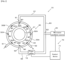
- FIG. 1 is a schematic diagram of a microwave plasma treatment device 10 according to this embodiment.
- the microwave plasma treatment device 10 is used to manufacture a large diamond substrate having a diameter of at least 100 mm or more, through CVD, for example.
- the microwave plasma treatment device 10 includes a single microwave oscillation source 20, a resonator 30, a waveguide 60, and a phase control mechanism 70.
- the microwave oscillation source 20 outputs microwaves to be supplied into a container 30A of the resonator 30.
- the microwave oscillation source 20 is a magnetron power source, for example.
- the center frequency of the microwaves output from the microwave oscillation source 20 is, 2.45 GHz, 915 MHz, or 10 GHz or more, for example.
- a microwave output from the microwave oscillation source 20 may be referred to as a "reference microwave”.
- the resonator 30 includes the container 30A, an outer circumferential waveguide 30B, a substrate support base 40, a source gas supply path 51, an exhaust path 52, and entrance windows 80.
- the container 30A is a vacuum container. Pressure inside the container 30A is in a range of 50 Torr to 200 Torr, for example.
- the shape of the container 30A can be selected as appropriate.
- the container 30A has a cylindrical shape.
- the outer circumferential waveguide 30B to be connected to the waveguide 60 is attached to a circumferential wall 32 of the container 30A.
- the outer circumferential waveguide 30B is shaped to surround the container 30A along the circumferential wall 32 of the container 30A.
- the substrate support base 40 is housed in an internal space 31 of the container 30A.
- a base member 100 for manufacturing a diamond substrate is placed on the substrate support base 40.
- the shape of the substrate support base 40 can be selected as appropriate.
- the substrate support base 40 is disk-shaped.
- a material constituting the base member 100 can be selected as appropriate as long as a film of carbon particles in later-described source gas is formed on the base member 100, and the material enables diamond having a diamond crystal structure to grow.
- Examples of the material constituting the base member 100 include single crystal diamond, polycrystalline diamond, silicon, 3C silicon carbide, gallium nitride, gallium oxide, iridium, platinum, nickel, magnesium oxide, yttrium-stabilized zirconia, and metals having a high melting point, such as molybdenum.
- the source gas supply path 51 supplies source gas for forming a diamond substrate to the internal space 31 in the container 30A.
- the source gas supply path 51 is connected to the circumferential wall 32 of the container 30A below or above the outer circumferential waveguide 30B in a height direction of the container 30A.
- Source gas is mixed gas containing carbon, hydrogen, nitrogen, and oxygen, for example.
- the exhaust path 52 is connected to the circumferential wall 32 of the container 30A below or above the outer circumferential waveguide 30B in the height direction of the container 30A, for example, so that gas inside the container 30A can be exhausted.
- An end portion of the exhaust path 52 opposite to the container 30A is connected to a vacuum pump (not shown). When the vacuum pump operates, the gas inside the container 30A passes through the exhaust path 52 and is exhausted to the outside of the container 30A.
- the waveguide 60 connects the microwave oscillation source 20 and the outer circumferential waveguide 30B to each other so that the reference microwave output from the microwave oscillation source 20 and a microwave obtained by modifying the phase of the reference microwave by the phase control mechanism 70 (hereinafter, may be referred to as a "modified microwave”) can be introduced into the container 30A.
- the waveguide 60 is a circular waveguide or rectangular waveguide, for example.
- the waveguide 60 includes a first portion 61 and a second portion 62.
- the first portion 61 and the second portion 62 are connected to the microwave oscillation source 20 via distributor 63.
- the reference microwave output from the microwave oscillation source 20 is distributed into the first portion 61 and the second portion 62 via distributor 63.
- the reference microwave which passes through the first portion 61 and is introduced into the outer circumferential waveguide 30B, is divided between one circumferential direction and the other circumferential direction of the outer circumferential waveguide 30B.
- Holes 32A are formed in the circumferential wall 32 of the container 30A.
- the number of holes 32A formed in the container 30A can be selected as appropriate. In this embodiment, eight holes 32A are formed in the container 30A at predetermined intervals along the circumferential direction. The number of holes 32A formed in the container 30A may be 1 to 7, or 9 or more.
- An entrance window 80 which allows transmission of mixed microwave of the reference microwave and the modified microwave, is fitted to each hole 32A.
- a material constituting the entrance window 80 is quartz glass or alumina, for example.
- the resonator 30 has a first-type introducing portion 91 and a second-type introducing portion 92.
- the first-type introducing portion 91 is a portion where the first portion 61 and the outer circumferential waveguide 30B are connected to each other, and introduces the reference microwave to the outer circumferential waveguide 30B without modifying the phase and amplitude of the reference microwave.
- the second-type introducing portion 92 is a portion where the second portion 62 and the outer circumferential waveguide 30B are connected to each other, and introduces the modified microwave to the outer circumferential waveguide 30B.
- the phase control mechanism 70 generates a modified microwave by modifying the phase of the reference microwave passing through the second portion 62.
- the phase control mechanism 70 includes a control device 71 and a phase shifter 72.
- the control device 71 is, for example, a PC (Personal Computer) or a PLC (Programmable Logic Controller), and controls the phase shifter 72 by outputting, to the phase shifter 72, a phase control signal based on a phase shifter control program.
- the phase shifter 72 is disposed in an intermediate portion of the second portion 62.
- the control device 71 controls the phase shifter 72 so as to modify the phase of the reference microwave passing through the phase shifter 72, such that the modified microwave is generated.
- the reference microwave that has passed through the first-type introducing portion 91, and the modified microwave that has passed through the second-type introducing portion 92 are introduced into the outer circumferential waveguide 30B, and thus the reference microwave and the modified microwave interfere with each other. Therefore, a region having a locally high electric field intensity is formed in the container 30A.
- the chemically active species include ions and radicals.
- the diameter of the plasma ball generated is 50 mm, for example.
- the control device 71 can change an electric field intensity distribution by controlling the phase shifter 72, in other words, by controlling the phase of the modified microwave, and as a result, at least one of the position, size, and shape of the plasma ball is controlled.
- the position of the plasma ball usually indicates the position of the plasma ball above the base member 100 in the container 30A.
- the size of the plasma ball is the diameter of the plasma ball.
- the shape of the plasma ball is an outer shape of the plasma ball.
- a basic outer shape of the plasma ball is a sphere, and an outer shape of a modified plasma ball is a flattened sphere, for example.
- Chemically active species contained in a plasma ball undergo reaction on the surface of the base member 100, diamond crystals are formed and grow, and thus a diamond substrate is manufactured.
- the manufactured diamond substrate includes the base member 100 and the diamond crystals formed on the base member 100.
- the relationships regarding the phases of the reference microwave and the modified microwave, the position of the plasma ball above the base member 100, the size of the plasma ball, and the shape of the plasma ball are obtained through simulation in advance.
- the simulation results may be stored in the control device 71 together with the phase shifter control program.
- the control device 71 vibrates the plasma ball above the base member 100, for example. In other words, the control device 71 dynamically moves the plasma ball above the base member 100. Therefore, a large-area diamond substrate can be formed.
- a part of the reference microwave output from a single microwave oscillation source 20 is introduced into the outer circumferential waveguide 30B via the first portion 61 and the first-type introducing portion 91.
- another part of the reference microwave is introduced into the second portion 62, and the phase thereof is modified by the phase shifter 72, and as a result, the reference microwave is converted into a modified microwave.
- the modified microwave is introduced into the outer circumferential waveguide 30B via the second portion 62 and the second-type introducing portion 92.
- the phase control mechanism 70 changes at least one of the position, size, and shape of the plasma ball in the container 30A by superimposing the modified microwave, which is introduced into the outer circumferential waveguide 30B via the second-type introducing portion 92, on the reference microwave introduced into the outer circumferential waveguide 30B via the first-type introducing portion 91.
- the microwave plasma treatment device 10 the phase and the like of the reference microwave passing through the first portion 61 are not modified, and thus it is possible to change the position, size, and shape of the plasma ball without disposing a phase shifter, an amplifier, and the like in the first portion 61. Therefore, a configuration thereof can be simplified. Also, because a phase shifter, an amplifier, and the like are not disposed in the first portion 61, manufacturing costs can be reduced.
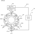
- a microwave plasma treatment device 210 according to a second embodiment will be described with reference to FIG. 2 .
- constituent elements that are the same as those in the first embodiment are given the same reference numerals, and their description will be omitted.
- FIG. 2 is a schematic diagram of a microwave plasma treatment device 210 according to this embodiment.
- the reference microwave output from a microwave oscillation source 20 is introduced into the outer circumferential waveguide 30B.
- a part of the reference microwave introduced into the outer circumferential waveguide 30B is converted into a modified microwave by a phase control mechanism 70, and is superimposed on the reference microwave.
- the microwave plasma treatment device 210 includes a port 270.
- the port 270 is connected to the outer circumferential waveguide 30B.
- a position where the port 270 is connected in the outer circumferential waveguide 30B can be selected as appropriate.
- the port 270 is connected thereto at a position of the outer circumferential waveguide 30B where the port 270 faces the first portion 61 via the container 30A.
- the number of ports 270 connected to the outer circumferential waveguide 30B can be selected as appropriate. In this embodiment, the number of ports 270 connected to the outer circumferential waveguide 30B is one. The number of ports 270 connected to the outer circumferential waveguide 30B may be two or more.
- the reference microwave output from the microwave oscillation source 20 is introduced into the outer circumferential waveguide 30B, and travels through the outer circumferential waveguide 30B.
- a part of the reference microwave introduced into the outer circumferential waveguide 30B is introduced into the port 270.
- the reference microwave introduced into the port 270 is reflected by a wall 271 at an end of the port 270 opposite to the container 30A, and passes through the phase shifter 72.
- the phase of the reference microwave that has passed through the phase shifter 72 is modified, and the reference microwave is converted into a modified microwave.
- the modified microwave is introduced into the outer circumferential waveguide 30B.
- the reference microwave and the modified microwave travel through the outer circumferential waveguide 30B, are mixed together, and introduced into the container 30A through a plurality of holes 32A and entrance windows 80.
- a part of the reference microwave introduced into the outer circumferential waveguide 30B is introduced into the port 270, and converted into a modified microwave.
- the modified microwave is mixed with the reference microwave in the outer circumferential waveguide 30B.
- the modified microwave is superimposed on the reference microwave, and thus an effect equivalent to that of the microwave plasma treatment device 10 according to the first embodiment can be obtained.
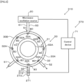
- a third embodiment differs from the second embodiment in a configuration of the phase control mechanism 70. Basically, other configurations are similar to those of the second embodiment.
- constituent elements that are the same as those in the second embodiment are given the same reference numerals, and their description will be omitted. The following mainly describes portions that are different from those in the second embodiment.
- FIG. 3 is a schematic diagram of a microwave plasma treatment device 310 according to this embodiment.
- the microwave plasma treatment device 310 includes a phase control mechanism 370.
- the phase control mechanism 370 includes a reflector 371 and a driving mechanism 372, which are disposed in a port 270.
- the reflector 371 reflects the reference microwave introduced into the port 270 toward the outer circumferential waveguide 30B.
- the driving mechanism 372 changes the position of the reflector 371 in the longitudinal direction of the port 270. Any configuration can be used for the driving mechanism 372.
- the driving mechanism 372 is a ball screw mechanism that includes a guide rail, a screw shaft that moves the reflector 371 along the guide rail, a motor that rotates the screw shaft, and the like.
- the control device 71 executes a driving mechanism control program regarding the operation of the driving mechanism 372 in response to a request from an operator.
- a relationship between the position of the reflector 371 in the port 270 and the phase of the modified microwave is obtained through simulation in advance.
- the simulation results may be stored in the control device 71 together with the driving mechanism control program.
- the relationships regarding the phases of the reference microwave and the modified microwave, the position of the plasma ball above the base member 100, the size of the plasma ball, and the shape of the plasma ball are obtained through simulation in advance.
- the simulation results may be stored in the control device 71.
- Each of the embodiments is an example of a form that the microwave plasma treatment device according to the present invention can take, and is not intended to limit the form.
- the microwave plasma treatment device according to the present invention can take a form different from those exemplified in each embodiment.
- An example thereof is a form in which some of constituent elements of each embodiment are replaced, changed, or omitted, or a new constituent element is added to each embodiment.
- some examples of variations of the embodiments will be described.
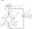
- the waveguide 60 may be configured to include a plurality of second portions 62, for example.
- phase shifters 72 are respectively disposed in the plurality of second portions 62.
- the number of first-type introducing portions 91 in the resonator 30 is one, and the number of second-type introducing portions 92 is two.
- FIG. 5 is a schematic diagram of a microwave plasma treatment device 10 that includes a resonator 530, which is a variation of the resonator 30 according to the first embodiment.
- the resonator 30 may be replaced with the resonator 530 having no outer circumferential waveguide 30B, and the first portion 61 and the second portion 62 may be connected to the container 30A, for example.
- a portion where the first portion 61 is connected to the container 30A constitutes a first-type introducing portion 91
- a portion where the second portion 62 is connected to the container 30A constitutes a second-type introducing portion 92.
- Entrance windows 80 are installed in the first-type introducing portion 91 and the second-type introducing portion 92. Also, in this variation, holes 32A in the circumferential wall 32 of the container 30A other than the portions connected to the waveguide 60 are closed. Note that this variation can also be applied to a variation of the first embodiment shown in FIG. 4 .
- a specific configuration of the resonator 30 can be changed as appropriate.
- the resonator 30 may be replaced with a resonator having no outer circumferential waveguide 30B, the first portion 61 may be connected to the container 30A, and the port 270 may be connected to the container 30A such that the reference microwave is introduced into the resonator 30A, for example.
- a portion where the first portion 61 is connected to the container 30A constitutes a first-type introducing portion 91
- a portion where the port 270 is connected to the container 30A constitutes a second-type introducing portion 92.
- Entrance windows 80 are installed in the first-type introducing portion 91 and the second-type introducing portion 92. Also, in this variation, holes 32A other than the portion of the container 30A connected to the first portion 61 and the portions connected to the port 270 are closed. In this variation, one or more ports 270 may be connected to the container 30A.
- the circumferential wall 32 of the container 30A may be omitted.
- a portion where the first portion 61 is connected to the outer circumferential waveguide 30B constitutes a first-type introducing portion 91
- a portion where the second portion 62 is connected to the outer circumferential waveguide 30B constitutes a second-type introducing portion 92.
- Entrance windows 80 are installed in the first-type introducing portion 91 and the second-type introducing portion 92.
- the outer circumferential waveguide 30B serves as the circumferential wall 32 of the container 30A. Note that this variation can also be applied to a variation of the first embodiment shown in FIG. 4 .
- the circumferential wall 32 of the container 30A may be omitted.
- a portion where the first portion 61 is connected to the outer circumferential waveguide 30B constitutes a first-type introducing portion 91
- a portion where the port 270 is connected to the outer circumferential waveguide 30B constitutes a second-type introducing portion 92.
- Entrance windows 80 are installed in the first-type introducing portion 91 and the second-type introducing portion 92.
- the outer circumferential waveguide 30B serves as the circumferential wall 32 of the container 30A.
- phase control mechanisms 70 and 370 may be any structure that is disposed in the container 30A and modifies the phase of the reference microwave introduced into the container 30A and reflects the modified microwave. Also, the phase control mechanisms 70 and 370 may be configured to change a radial shape of the circumferential wall 32 of the container 30A. In short, the phase control mechanisms 70 and 370 can have any configuration as long as a modified microwave whose phase is different from the phase of the reference microwave can be generated by controlling the phase of a part of the reference microwave introduced into the resonator 30.
- a shape in which the circumferential wall 32 of the container 30A is connected to the microwave oscillation source 20 is also possible by omitting the waveguide 60 and the outer circumferential waveguide 30B.
- phase control mechanism 70 and the phase control mechanism 370 can be combined.
- a phase shifter 72 may be disposed in any port 270, and the reflector 371 and the driving mechanism 372 may be disposed in any other port 270.
- the phase shifter 72 and the driving mechanism 372 may be controlled by a single control device 71, or control devices may respectively control the phase shifter 72 and the driving mechanism 372.
- microwave plasma treatment devices 10, 210, and 310 are used to manufacture a diamond substrate, these devices can also be used to manufacture other substrates by changing source gas and conditions such as plasma transfer periods.
Landscapes
- Physics & Mathematics (AREA)
- Engineering & Computer Science (AREA)
- Chemical & Material Sciences (AREA)
- Plasma & Fusion (AREA)
- Spectroscopy & Molecular Physics (AREA)
- Mechanical Engineering (AREA)
- Chemical Kinetics & Catalysis (AREA)
- Materials Engineering (AREA)
- General Chemical & Material Sciences (AREA)
- Metallurgy (AREA)
- Organic Chemistry (AREA)
- Electromagnetism (AREA)
- Analytical Chemistry (AREA)
- Chemical Vapour Deposition (AREA)
- Plasma Technology (AREA)
- Drying Of Semiconductors (AREA)
Applications Claiming Priority (2)
| Application Number | Priority Date | Filing Date | Title |
|---|---|---|---|
| JP2021011549 | 2021-01-27 | ||
| PCT/JP2022/002724 WO2022163661A1 (ja) | 2021-01-27 | 2022-01-25 | マイクロ波プラズマ処理装置 |
Publications (2)
| Publication Number | Publication Date |
|---|---|
| EP4287784A1 true EP4287784A1 (de) | 2023-12-06 |
| EP4287784A4 EP4287784A4 (de) | 2025-01-01 |
Family
ID=82653596
Family Applications (1)
| Application Number | Title | Priority Date | Filing Date |
|---|---|---|---|
| EP22745881.7A Pending EP4287784A4 (de) | 2021-01-27 | 2022-01-25 | Mikrowellenplasmabehandlungsvorrichtung |
Country Status (5)
| Country | Link |
|---|---|
| US (1) | US12324085B2 (de) |
| EP (1) | EP4287784A4 (de) |
| JP (1) | JP7582695B2 (de) |
| CN (1) | CN116670325A (de) |
| WO (1) | WO2022163661A1 (de) |
Families Citing this family (1)
| Publication number | Priority date | Publication date | Assignee | Title |
|---|---|---|---|---|
| JP7582695B2 (ja) * | 2021-01-27 | 2024-11-13 | 国立研究開発法人産業技術総合研究所 | マイクロ波プラズマ処理装置 |
Family Cites Families (36)
| Publication number | Priority date | Publication date | Assignee | Title |
|---|---|---|---|---|
| JPH01184921A (ja) * | 1988-01-20 | 1989-07-24 | Canon Inc | エッチング、アッシング及び成膜等に有用なプラズマ処理装置 |
| JPH01222057A (ja) * | 1988-02-29 | 1989-09-05 | Sumitomo Electric Ind Ltd | 薄膜形成方法および感光体 |
| JPH0810634B2 (ja) | 1990-06-01 | 1996-01-31 | インターナショナル・ビジネス・マシーンズ・コーポレイション | マイクロ波給電式材料/プラズマ処理システム |
| JP3129814B2 (ja) * | 1992-01-17 | 2001-01-31 | 新日本無線株式会社 | マイクロ波プラズマ装置 |
| JPH065386A (ja) * | 1992-06-19 | 1994-01-14 | Kobe Steel Ltd | 電子サイクロトロン共鳴装置 |
| JP4852997B2 (ja) * | 2005-11-25 | 2012-01-11 | 東京エレクトロン株式会社 | マイクロ波導入装置及びプラズマ処理装置 |
| JP4677918B2 (ja) * | 2006-02-09 | 2011-04-27 | 東京エレクトロン株式会社 | プラズマ処理装置及びプラズマ処理方法 |
| WO2008013112A1 (en) * | 2006-07-28 | 2008-01-31 | Tokyo Electron Limited | Microwave plasma source and plasma processing apparatus |
| WO2010004997A1 (ja) * | 2008-07-11 | 2010-01-14 | 東京エレクトロン株式会社 | プラズマ処理装置 |
| JP2012089334A (ja) * | 2010-10-19 | 2012-05-10 | Tokyo Electron Ltd | マイクロ波プラズマ源およびプラズマ処理装置 |
| JP5921241B2 (ja) * | 2011-03-10 | 2016-05-24 | 国立大学法人名古屋大学 | プラズマ生成装置、プラズマ処理装置及びプラズマ処理方法 |
| JP5893865B2 (ja) * | 2011-03-31 | 2016-03-23 | 東京エレクトロン株式会社 | プラズマ処理装置およびマイクロ波導入装置 |
| JP5836144B2 (ja) * | 2012-01-31 | 2015-12-24 | 東京エレクトロン株式会社 | マイクロ波放射機構および表面波プラズマ処理装置 |
| JP6356415B2 (ja) * | 2013-12-16 | 2018-07-11 | 東京エレクトロン株式会社 | マイクロ波プラズマ源およびプラズマ処理装置 |
| GB201410703D0 (en) * | 2014-06-16 | 2014-07-30 | Element Six Technologies Ltd | A microwave plasma reactor for manufacturing synthetic diamond material |
| JP6404111B2 (ja) * | 2014-12-18 | 2018-10-10 | 東京エレクトロン株式会社 | プラズマ処理装置 |
| JP6671166B2 (ja) * | 2015-12-15 | 2020-03-25 | 東京エレクトロン株式会社 | 絶縁膜積層体の製造方法 |
| JP6697292B2 (ja) * | 2016-03-14 | 2020-05-20 | 東京エレクトロン株式会社 | プラズマ処理装置及びプラズマ処理方法 |
| JP6752117B2 (ja) * | 2016-11-09 | 2020-09-09 | 東京エレクトロン株式会社 | マイクロ波プラズマ源およびマイクロ波プラズマ処理装置 |
| JP6749258B2 (ja) * | 2017-01-31 | 2020-09-02 | 東京エレクトロン株式会社 | マイクロ波プラズマ源、マイクロ波プラズマ処理装置、およびプラズマ処理方法 |
| JP6890459B2 (ja) * | 2017-04-14 | 2021-06-18 | 東京エレクトロン株式会社 | プラズマ処理装置及び制御方法 |
| US11037764B2 (en) * | 2017-05-06 | 2021-06-15 | Applied Materials, Inc. | Modular microwave source with local Lorentz force |
| KR102401446B1 (ko) * | 2017-08-31 | 2022-05-24 | 에이에스엠 아이피 홀딩 비.브이. | 기판 처리 장치 |
| JP6960813B2 (ja) * | 2017-09-20 | 2021-11-05 | 東京エレクトロン株式会社 | グラフェン構造体の形成方法および形成装置 |
| CN107754572A (zh) * | 2017-11-21 | 2018-03-06 | 清华大学 | 一种微波等离子体工业有机废气处理系统 |
| DE102018000401A1 (de) * | 2018-01-19 | 2019-07-25 | Ralf Spitzl | Mikrowellenplasmavorrichtung |
| US11081317B2 (en) * | 2018-04-20 | 2021-08-03 | Applied Materials, Inc. | Modular high-frequency source |
| US11393661B2 (en) * | 2018-04-20 | 2022-07-19 | Applied Materials, Inc. | Remote modular high-frequency source |
| US11862432B2 (en) * | 2018-07-02 | 2024-01-02 | Mitsubishi Electric Corporation | Microwave heating device |
| US12159788B2 (en) * | 2020-12-14 | 2024-12-03 | Asm Ip Holding B.V. | Method of forming structures for threshold voltage control |
| TW202226899A (zh) * | 2020-12-22 | 2022-07-01 | 荷蘭商Asm Ip私人控股有限公司 | 具匹配器的電漿處理裝置 |
| JP7582695B2 (ja) * | 2021-01-27 | 2024-11-13 | 国立研究開発法人産業技術総合研究所 | マイクロ波プラズマ処理装置 |
| JP2022150627A (ja) * | 2021-03-26 | 2022-10-07 | 東京エレクトロン株式会社 | プラズマ処理装置及びプラズマ処理方法 |
| KR102932767B1 (ko) * | 2021-08-27 | 2026-03-05 | 삼성전자주식회사 | 플라즈마 발생 장치 |
| JP7632975B2 (ja) * | 2021-09-17 | 2025-02-19 | 東京エレクトロン株式会社 | プラズマ処理装置及びプラズマ処理方法 |
| US12014898B2 (en) * | 2021-09-27 | 2024-06-18 | Applied Materials, Inc. | Active temperature control for RF window in immersed antenna source |
-
2022
- 2022-01-25 JP JP2022578418A patent/JP7582695B2/ja active Active
- 2022-01-25 CN CN202280008772.2A patent/CN116670325A/zh active Pending
- 2022-01-25 EP EP22745881.7A patent/EP4287784A4/de active Pending
- 2022-01-25 WO PCT/JP2022/002724 patent/WO2022163661A1/ja not_active Ceased
- 2022-01-25 US US18/274,422 patent/US12324085B2/en active Active
Also Published As
| Publication number | Publication date |
|---|---|
| CN116670325A (zh) | 2023-08-29 |
| WO2022163661A1 (ja) | 2022-08-04 |
| US20240098866A1 (en) | 2024-03-21 |
| US12324085B2 (en) | 2025-06-03 |
| JPWO2022163661A1 (de) | 2022-08-04 |
| EP4287784A4 (de) | 2025-01-01 |
| JP7582695B2 (ja) | 2024-11-13 |
Similar Documents
| Publication | Publication Date | Title |
|---|---|---|
| RU2666135C2 (ru) | Свч-плазменный реактор для изготовления синтетического алмазного материала | |
| JP5882777B2 (ja) | 成膜装置 | |
| KR100381752B1 (ko) | 플라즈마 프로세스 장치 | |
| KR102301412B1 (ko) | 플라즈마 처리 장치 | |
| US20050173069A1 (en) | Plasma generating apparatus and plasma processing apparatus | |
| JP2014165402A (ja) | 窒化膜を形成する方法 | |
| TW201844064A (zh) | 具有局部勞侖茲力的模組化微波源 | |
| US6592664B1 (en) | Method and device for epitaxial deposition of atoms or molecules from a reactive gas on a deposition surface of a substrate | |
| EP4287784A1 (de) | Mikrowellenplasmabehandlungsvorrichtung | |
| CN113195785A (zh) | 从成角度的气体流辅助的等离子体的轴对称材料沉积 | |
| JPH10189293A (ja) | プラズマ処理装置 | |
| JP2003142460A (ja) | プラズマ処理装置 | |
| JPH04337076A (ja) | 高圧力下でのプラズマ及びラジカルcvd法による高速成膜方法 | |
| US11066748B2 (en) | Microwave plasma and ultraviolet assisted deposition apparatus and method for material deposition using the same | |
| Dahiya et al. | Experimental investigation of an electronegative cylindrical capacitively coupled geometrically asymmetric plasma discharge with an axisymmetric magnetic field | |
| WO2021131097A1 (ja) | マイクロ波プラズマ処理装置 | |
| KR102886353B1 (ko) | 저온 기판 보호 층 생성 | |
| EP4539245A1 (de) | Mikrowellenplasma-cvd-vorrichtung | |
| WO2025197982A1 (ja) | マイクロ波プラズマ処理装置、プラズマ発生方法 | |
| JP7802350B2 (ja) | マイクロ波モード変換器 | |
| KR20220087971A (ko) | 다이아몬드 합성용 마이크로파 플라즈마 cvd 장치 | |
| JP2026043830A (ja) | ダイヤモンド基板の製造方法、ダイヤモンド基板 | |
| CN118773584A (zh) | 一种基于环形驻波谐振腔的并行mpcvd装置及方法 | |
| JP2023179963A (ja) | マイクロ波プラズマcvd装置 | |
| TW202536231A (zh) | 奈米晶形鑽石薄膜之低溫氣相沉積 |
Legal Events
| Date | Code | Title | Description |
|---|---|---|---|
| STAA | Information on the status of an ep patent application or granted ep patent |
Free format text: STATUS: THE INTERNATIONAL PUBLICATION HAS BEEN MADE |
|
| PUAI | Public reference made under article 153(3) epc to a published international application that has entered the european phase |
Free format text: ORIGINAL CODE: 0009012 |
|
| STAA | Information on the status of an ep patent application or granted ep patent |
Free format text: STATUS: REQUEST FOR EXAMINATION WAS MADE |
|
| 17P | Request for examination filed |
Effective date: 20230815 |
|
| AK | Designated contracting states |
Kind code of ref document: A1 Designated state(s): AL AT BE BG CH CY CZ DE DK EE ES FI FR GB GR HR HU IE IS IT LI LT LU LV MC MK MT NL NO PL PT RO RS SE SI SK SM TR |
|
| DAV | Request for validation of the european patent (deleted) | ||
| DAX | Request for extension of the european patent (deleted) | ||
| A4 | Supplementary search report drawn up and despatched |
Effective date: 20241128 |
|
| RIC1 | Information provided on ipc code assigned before grant |
Ipc: H01J 37/32 20060101ALI20241125BHEP Ipc: C23C 16/511 20060101ALI20241125BHEP Ipc: H05H 1/46 20060101AFI20241125BHEP |