EP4268552B1 - Dispositif de refroidissement destiné au refroidissement d'un module semi-conducteur et onduleur pourvu de dispositif de refroidissement - Google Patents
Dispositif de refroidissement destiné au refroidissement d'un module semi-conducteur et onduleur pourvu de dispositif de refroidissement Download PDFInfo
- Publication number
- EP4268552B1 EP4268552B1 EP22706045.6A EP22706045A EP4268552B1 EP 4268552 B1 EP4268552 B1 EP 4268552B1 EP 22706045 A EP22706045 A EP 22706045A EP 4268552 B1 EP4268552 B1 EP 4268552B1
- Authority
- EP
- European Patent Office
- Prior art keywords
- cooling
- semiconductor module
- base body
- face
- cover
- Prior art date
- Legal status (The legal status is an assumption and is not a legal conclusion. Google has not performed a legal analysis and makes no representation as to the accuracy of the status listed.)
- Active
Links
Images
Classifications
-
- H—ELECTRICITY
- H05—ELECTRIC TECHNIQUES NOT OTHERWISE PROVIDED FOR
- H05K—PRINTED CIRCUITS; CASINGS OR CONSTRUCTIONAL DETAILS OF ELECTRIC APPARATUS; MANUFACTURE OF ASSEMBLAGES OF ELECTRICAL COMPONENTS
- H05K7/00—Constructional details common to different types of electric apparatus
- H05K7/20—Modifications to facilitate cooling, ventilating, or heating
- H05K7/2039—Modifications to facilitate cooling, ventilating, or heating characterised by the heat transfer by conduction from the heat generating element to a dissipating body
- H05K7/20509—Multiple-component heat spreaders; Multi-component heat-conducting support plates; Multi-component non-closed heat-conducting structures
-
- H—ELECTRICITY
- H05—ELECTRIC TECHNIQUES NOT OTHERWISE PROVIDED FOR
- H05K—PRINTED CIRCUITS; CASINGS OR CONSTRUCTIONAL DETAILS OF ELECTRIC APPARATUS; MANUFACTURE OF ASSEMBLAGES OF ELECTRICAL COMPONENTS
- H05K7/00—Constructional details common to different types of electric apparatus
- H05K7/20—Modifications to facilitate cooling, ventilating, or heating
- H05K7/2089—Modifications to facilitate cooling, ventilating, or heating for power electronics, e.g. for inverters for controlling motor
- H05K7/209—Heat transfer by conduction from internal heat source to heat radiating structure
-
- H—ELECTRICITY
- H05—ELECTRIC TECHNIQUES NOT OTHERWISE PROVIDED FOR
- H05K—PRINTED CIRCUITS; CASINGS OR CONSTRUCTIONAL DETAILS OF ELECTRIC APPARATUS; MANUFACTURE OF ASSEMBLAGES OF ELECTRICAL COMPONENTS
- H05K7/00—Constructional details common to different types of electric apparatus
- H05K7/20—Modifications to facilitate cooling, ventilating, or heating
- H05K7/2089—Modifications to facilitate cooling, ventilating, or heating for power electronics, e.g. for inverters for controlling motor
- H05K7/20909—Forced ventilation, e.g. on heat dissipaters coupled to components
-
- H—ELECTRICITY
- H05—ELECTRIC TECHNIQUES NOT OTHERWISE PROVIDED FOR
- H05K—PRINTED CIRCUITS; CASINGS OR CONSTRUCTIONAL DETAILS OF ELECTRIC APPARATUS; MANUFACTURE OF ASSEMBLAGES OF ELECTRICAL COMPONENTS
- H05K7/00—Constructional details common to different types of electric apparatus
- H05K7/20—Modifications to facilitate cooling, ventilating, or heating
- H05K7/2089—Modifications to facilitate cooling, ventilating, or heating for power electronics, e.g. for inverters for controlling motor
- H05K7/20927—Liquid coolant without phase change
Definitions
- the invention relates to a cooling device with a semiconductor module for cooling the semiconductor module and a converter with the cooling device.
- converters can have several converter modules and converter systems can have several converters, which can be similar in terms of their functionality and electrical dimensions, but can also have differences.
- Standardized coupling mechanisms for example using backplane buses, should and can bring such converters or converter systems very close together in terms of technology and space.
- Siemens SINAMICS S120 converter series in booksize format.
- the converter or its converter modules have a geometric or clear structure in a book format.
- the height and depth of the design of this inverter series are currently essentially fixed, but the width can vary. The width therefore offers the potential to further minimize the installation space.
- Components in converters which often require a relatively large amount of installation space, are heat sinks or cooling devices for dissipating heat from electrical or electronic components in combination with these components.
- the minimum width of the converter series mentioned is mainly determined by the design of the cooling device with the heat sink and the semiconductor module connected to the heat sink for operational heat dissipation.
- a semiconductor module is understood to be both a semiconductor module with a single semiconductor and a semiconductor module in the form of a bridge circuit with several semiconductors - such as in a six-pulse bridge circuit (B6 bridge).
- Typical semiconductors are IGBTs (Insulated-Gate Bipolar Transistor) or MOSFETs (Metal Oxide Semiconductor Field-Effect Transistor) designed as power semiconductors.
- CN 108 966 482 A discloses a semiconductor module placed on a circuit board and covered by a heat sink having cooling fins surrounding the semiconductor module so that air can flow around the module and the space between the circuit board and the heat sink is effectively cooled.
- the invention is based on the object of proposing a cooling device for cooling a semiconductor module and a converter with the cooling device, which require less space than the prior art.
- the object is achieved by a cooling device having the features specified in claim 1 and by a converter having the features specified in claim 14.
- a cooling device with a semiconductor module and a heat sink for cooling the semiconductor module wherein the semiconductor module has a first and second cover surface and a plurality of side surfaces, wherein the first faces away from the second cover surface, wherein a module space of the semiconductor module is formed between the cover surfaces, which is enclosed by the side surfaces, wherein the heat sink has a base body, wherein cooling elements protruding from the base body are formed on a first surface of the base body, wherein the semiconductor module is connected to the first surface of the base body at the first cover surface and the semiconductor module is embedded between at least some of the cooling elements.
- the cooling elements are aligned and arranged in such a way that the semiconductor module to be cooled is arranged with as large an area as possible, in particular its side surfaces, in the flow direction and can thus be flowed around and cooled by the cooling medium according to the invention.
- At least a first and a second side surface of the side surfaces of the semiconductor module form a common side edge and the common side edge of the first and second side surfaces faces the flow direction.
- the cooling medium flowing in the direction of flow can break so that it splits and can, for example, flow around and dissipate heat from both side surfaces of the semiconductor module in the manner according to the invention.
- the construction volume and thus the space requirement of the construction according to the invention comprising the heat sink, cooling elements and semiconductor module is reduced in an advantageous manner compared to a known construction in which the cooling elements are not formed on the first surface of the base body designated as the mounting surface of the semiconductor module and are therefore not arranged together with the semiconductor module by means of this special construction topology.
- embedding is understood here in the spatial sense to mean enclosing, enclosing, surrounding or limiting the semiconductor module, particularly on its side surfaces, by the cooling elements.
- An embedding space for the semiconductor module created in this way is also limited at least by the first surface of the base body of the heat sink.
- a single semiconductor or several semiconductors for example in the form of a B6 bridge circuit, can be arranged in the formed module space of the semiconductor module.
- the number of side surfaces that form the modular space is not limited, but at least three side surfaces are provided.
- the cooling elements are designed as cooling fins or pin fins or a combination of cooling fins and pin fins.
- pin fin is a term that has now become technically established in connection with heat sinks. It describes pin-like bulges on heat sinks, which, compared to conventional cooling fins, are usually smaller and can be distributed more finely on the surface of a heat sink as a single pin fin.
- a convection current can generally be advantageously channeled in one direction over the heat sink, whereby pin fins, thanks to their fine-grained arrangement option, can also advantageously thin out a convection current at specific locations or, by generating local vortices, strengthen it.
- cooling fins may be more effective.
- the semiconductor module is connected at its second cover surface to a component carrier element, in particular a printed circuit board.
- the semiconductor module is usually electrically connected via the component carrier element, preferably the circuit board.
- the advantageous arrangement of the semiconductor module between the first surface of the base body and the component carrier element further advantageously reduces the space required to connect the semiconductor module to the heat sink.
- a busbar or another electrical conductor can also be used as a component carrier element, to which the semiconductor module is then attached.
- the cooling device has a cooling element cover, wherein the cooling elements each form a cooling element end facing away from the base body and at least some of the cooling elements are connected to the cooling element cover at their cooling element end
- directed cooling channels can be better sealed off from the surroundings of the cooling device, whereby convection can be guided more specifically past at least the side surfaces of the semiconductor module and thus the semiconductor module can be advantageously cooled.
- the cooling element cover is made of the same metallic material as the base body of the heat sink and/or the cooling elements.
- the cooling element cover thus also has the usually very good thermal cooling properties of the base body and/or the cooling elements due to the metallic nature, so that an improved dissipation of the waste heat generated during operation of the semiconductor module to the environment of the cooling device can advantageously be carried out.
- the heat sink is formed monolithically from the base body, the cooling elements and the cooling element cover.
- the monolithic structure presented in this way enables a cooling device that can be manufactured compactly and cost-effectively on an industrial scale.
- a recess can be provided in the cover plate for introducing the semiconductor module during manufacture of the cooling device.
- the cooling element cover is designed as a component carrier element, in particular as a printed circuit board.
- a basic functionality of the component carrier element / especially the circuit board is to provide electronic and electrotechnical components, such as the semiconductor module, with an electrical and mechanical connection within an electrical device, such as the converter. Accordingly, the component carrier element / circuit board is generally an inherent part of the converter.
- the combination with another function, that of covering the cooling elements, advantageously reduces the space required for the cooling device and can help to advantageously reduce the dimensions and thus the installation space volume of converters.
- component carrier element / circuit board as a cooling element cover may make it necessary to electrically isolate the component carrier element / circuit board from the cooling elements.
- the cooling elements and the side surfaces of the semiconductor module can be flowed around in a flow direction along the base body by means of a cooling medium.
- the cooling medium is liquid, in particular water, or gaseous, in particular air.
- an edge angle at the common side edge between the first and second side surface has a value in an angular range of 30° to 60°, in particular of 45°.
- edge angle in the range of 30° to 60° makes the flow around the side surfaces particularly effective, since on the one hand the cooling medium does not accumulate on the side surfaces, and on the other hand the cooling medium does not flow past the side surfaces too quickly without the heat loss to be able to absorb and transport the material sufficiently away from the semiconductor module.
- a preferred value for the edge angle is 45°, which is structurally specified for a four-sided, rectangular semiconductor module.
- a maximum cooling element length of the cooling elements formed on the first surface of the base body, starting from the first surface of the base body to the cooling element end of the respective cooling element, is limited by a cover surface distance between the first cover surface and the second cover surface of the semiconductor module.
- the semiconductor module One of the components that determine the overall width of the cooling device is the semiconductor module. Since it is a component that is usually available on the market in its specific dimensions and is therefore predetermined, the cooling elements in particular must be based on the specified dimensions of the semiconductor module.
- cover surfaces mentioned here in addition to the side surfaces, represent the external dimensions of the semiconductor module, whereby electrical connections for contacting the semiconductor module or mechanical fastening means can be excluded from this consideration.
- a second surface of the base body facing away from the first surface of the base body is free of cooling elements.
- a forced convection of the cooling medium can be generated by a convection generator.
- Forced convection forces the cooling of the semiconductor module by allowing the cooling medium to be transported more precisely, more quickly and in larger volumes to the semiconductor module to be cooled and to be transported away from it by absorbing the heat loss generated by the semiconductor module during operation.
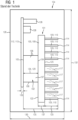
- FIG 1 shows a schematic sectional view of a known cooling device 101, which is integrated into a converter housing 126 of a converter 134.
- a semiconductor module 102 is connected to the base body 108 via its first cover surface 104.
- the semiconductor module 102 is also connected to a component carrier element 112, here a printed circuit board 113, via its second cover surface 105.
- the semiconductor module 102 forms a module space 107, which is determined by the first and second cover surfaces 104, 105 and the side surfaces 106.
- the component carrier element 112 / the circuit board 113 has further electronic components 128, which are arranged away from the cooling device 101, but are integrated with the component carrier element 112 / the circuit board 113 into the converter housing 126 of the converter 134.
- cooling elements 109 in the form of cooling fins 110 are formed, which protrude orthogonally from the base body 108.
- the cooling elements 109 and the second surface 125 of the base plate 108 of the heat sink 103 are surrounded by a cooling medium 117.
- the illustration of the converter housing 126 of the converter 134 shows a view of the converter housing 126, which reveals a housing width 130 and a housing height 132 of the converter housing 126.
- the housing width 130 of the converter housing 126 of the converter 124 is, as FIG 1 also evidently shows, is essentially determined by a cooling device width 135 of the cooling device 101.
- This cooling device width 135 sums up a module height 129 of the semiconductor module 102, a second thickness 137 of the base body 108 of the heat sink 103 and a maximum cooling element length 123 of the cooling elements 109, here the cooling fins 110.
- the module height 129 is determined by the cover surface distance 124 of the first cover surface 104 from the second cover surface 105 and the maximum cooling element length 123 is determined by a distance of the second surface 125 of the base body 108 from a cooling element end 114 assigned to the respective cooling element 109, which in each case faces away from the second surface 125 of the base body 108.
- the first thickness 136 of the component carrier element 112, here the circuit board 113, can be added to the cooling device width 135 in order to be able to make a comparison with the housing width 130 of the converter housing 126.
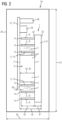
- FIG 2 a first schematic sectional view of a cooling device 1 according to the invention is shown, which is integrated into a converter housing 26 of a converter 34 according to the invention.
- a semiconductor module 2 is connected to the base body 8 via its first cover surface 4.
- the semiconductor module 2 is also connected to a component carrier element 12, here a printed circuit board 13, via its second cover surface 5.
- the semiconductor module 2 forms a module space 7, which is determined by the first and second cover surfaces 4, 5 and the side surfaces 6.
- the component carrier element 12 / the circuit board 13 has further electronic components 28, which are arranged away from the cooling device 1, but are integrated with the component carrier element 12 / the circuit board 13 in the converter housing 6 of the converter 4.
- Cooling elements 9 in the form of cooling fins 10 are also formed on the first surface 22 of the base body 8 of the heat sink 3, which here protrude orthogonally from the base body 8, whereby the semiconductor module 2 is embedded by the cooling elements 9.
- a cooling medium 17 flows around both the semiconductor module 2 and the cooling elements 9 and the first surface 22 of the base body 8 of the heat sink 3.
- the illustration of the converter housing 26 of the converter 34 shows a view of the converter housing 26, which reveals a housing width 30 and a housing height 32 of the converter housing 26.
- the housing width 30 of the converter housing 26 of the converter 24 is, as FIG 2 also evidently shows, essentially determined by a cooling device width 35 of the cooling device 1.
- This cooling device width 35 sums up a module height 29 of the semiconductor module 2 and a second thickness 37 of the base body 8 of the heat sink 3.
- the cooling elements 9 are smaller here than the module height 29 of the semiconductor module 2 with regard to their maximum cooling element length 23.
- the cooling element length 23 therefore does not exceed the module height 29 of the semiconductor module 2 and therefore does not influence the determined cooling device width 35 of the cooling device 1.
- the module height 29 is determined by the cover surface distance 24 of the first cover surface 4 from the second cover surface 5.
- the maximum cooling element length 23 of the cooling elements 9 is determined by a distance of the first surface 22 of the base body 8 from a cooling element end 14 assigned to the respective cooling element 9, which in each case faces away from the first surface 22 of the base body 8.
- the first thickness 36 of the component carrier element 12, here the circuit board 13, can be added to the cooling device width 35 in order to be able to make a comparison with the housing width 30 of the converter housing 26.
- a comparison of the cooling device width 35 of the cooling device 1 according to the invention from FIG 2 to the cooling device width 135 of the known cooling device 101 from FIG 1 also clearly shows that the cooling device width 35 of the cooling device 1 according to the invention FIG 2 significantly compared to the cooling device width 135 of the known cooling device 101 from FIG 1 is reduced.
- the housing width 30 of the converter housing 26 of the converter 34 according to the invention clearly compared to the housing width 130 of the converter housing 126 of the known converter 134, as in FIG 1 shown, can be reduced.
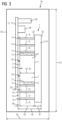
- FIG 3 a second schematic sectional view of the cooling device 1 according to the invention integrated into the converter housing 26 of the converter 34 according to the invention is shown FIG 2 shown.
- the second schematic sectional view from FIG 3 essentially corresponds to the first schematic sectional view from FIG 2 , thus FIG 3 analogous to FIG 2 , but with the difference that the cooling device 1 has a cooling element cover 15.
- This cooling element cover 15 is connected to the cooling elements 9, here the cooling fins 10, via their cooling element ends 14.
- the cooling element cover 15 also extends over the semiconductor module 2 and is here connected to the semiconductor module 2 via the second cover surface 5 of the semiconductor module 2.
- the semiconductor module 2 is connected at its second cover surface 5 only via two electrical vias 33 shown as an example to the component carrier element 12, here the printed circuit board 13
- the representation of the converter housing 26 of the converter 34 in FIG 3 shows a view of the converter housing 26, which reveals a housing width 30 and a housing height 32 of the converter housing 26.
- the housing width 30 of the converter housing 26 of the converter 24 is, as FIG 3 also evidently shows, is essentially determined by a cooling device width 35 of the cooling device 1.
- This cooling device width 35 sums up the module height 29 of the semiconductor module 2, the second thickness 37 of the base body 8 of the heat sink 3 and a third thickness 38 of the cooling element cover 15.
- the cooling elements 9 are here the same size as the module height 29 of the semiconductor module 2 with regard to their maximum cooling element length 23.
- the module height 29 is determined by the cover surface distance 24 of the first cover surface 4 from the second cover surface 5.
- the maximum cooling element length 23 of the cooling elements 9 is determined by a distance of the first surface 22 of the base body 8 from a cooling element end 14 assigned to the respective cooling element 9, which in each case faces away from the first surface 22 of the base body 8.
- the first thickness 36 of the component carrier element 12, here the circuit board 13, can be added to the cooling device width 35 in order to be able to make a comparison with the housing width 30 of the converter housing 26.
- a comparison of the cooling device width 35 of the cooling device 1 according to the invention from FIG 3 to the cooling device width 135 of the known cooling device 101 from FIG 1 clearly shows that the cooling device width 35 of the cooling device 1 according to the invention FIG 3 significantly compared to the cooling device width 135 of the known cooling device 101 from FIG 1 is reduced.
- the housing width 30 of the converter housing 26 of the converter 34 according to the invention clearly compared to the housing width 130 of the converter housing 126 of the known converter 134, as in FIG 1 shown, can be reduced.
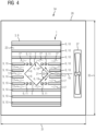
- FIG 4 shows a schematic detailed representation of the cooling device 1 according to the invention, integrated in the converter housing 26 of the converter 34 according to the invention according to FIG 2 and FIG 3 .
- the cooling device 1 is shown here in a side view. Cooling elements 9 in a combination of cooling fins 10 and pin fins 11 are formed on the first surface 22 of the base plate 8 of the heat sink 3. The semiconductor module 2 connected to the first surface 22 of the base plate 8 is embedded by the cooling elements 9.
- a first side surface 18 of the side surfaces 6 forms with the second side surface 19 of the side surfaces 6 a common side edge 20 which faces the flow direction 16, wherein the facing of the first to the second side surface 18,19 is determined by an edge angle 21.
- This edge angle 21 influences the flow direction 16 as the cooling medium 17 flows past the first and second side surfaces 18, 19 of the semiconductor module 2 and thus the cooling effect of the cooling medium 17 on the first and second side surfaces 18, 19 of the semiconductor module 2.
- a convection generator 27 for example a fan for the cooling medium 17, which is gaseous, or a pump for the cooling medium 17, which is liquid, generates a forced convection of the cooling medium 17 along the flow direction 16.
- the schematic detailed representation shows a specific view of the converter housing 26 of the converter 34, which reveals a housing depth 31 and a housing height 32 of the converter housing 26.
Landscapes
- Engineering & Computer Science (AREA)
- Microelectronics & Electronic Packaging (AREA)
- Physics & Mathematics (AREA)
- Thermal Sciences (AREA)
- Cooling Or The Like Of Electrical Apparatus (AREA)
- Cooling Or The Like Of Semiconductors Or Solid State Devices (AREA)
Claims (13)
- Dispositif (1) de refroidissement comprenant un module (2) à semiconducteur et un puits (3) de chaleur pour le refroidissement du module (2) à semiconducteur,
dans lequel- le module (2) à semiconducteur a une première et une deuxième surface (4, 5) de recouvrement et plusieurs surfaces (6) latérales,- la première n'est pas tournée vers la deuxième surface (4, 5) de recouvrement,- entre les surfaces (4, 5) de recouvrement, est constitué un espace (7) de module du module (2) à semiconducteur, qui est entouré par les surfaces (6) latérales,- le puits (3) de chaleur a un corps (8) de base,- sur une première surface (22) du corps (8) de base, sont constitués des éléments (9) de refroidissement en saillie du corps (8) de base,- le module (2) à semiconducteur est relié à la première surface (4) de recouvrement par la première surface (22) du corps (8) de base,- le module (2) à semiconducteur est inséré entre au moins certains des éléments (9) de refroidissement,- autour des éléments (9) de refroidissement et des surfaces (6) latérales du module (2) à semiconducteur peut s'écouler, dans un sens (16) d'écoulement le long du corps (8) de base, au moins un fluide (17) de refroidissement et le dispositif de refroidissement est caractérisé en ce que- au moins une première et une deuxième surfaces (18, 19) latérales, parmi les surfaces (6) latérales du module (2) à semiconducteur, forment une arête (20) latérale commune et l'arête (20) latérale commune à la première et à la deuxième surfaces (18, 19) latérales est tournée vers le sens (16) d'écoulement. - Dispositif (1) de refroidissement suivant la revendication 1, dans lequel les éléments (9) de refroidissement sont constitués sous la forme d'ailettes (10) de refroidissement ou de pin fins (11) ou d'une combinaison d'ailettes (10) de refroidissement et de pin fins (11).
- Dispositif (1) de refroidissement suivant l'une des revendications 1 ou 2, dans lequel le module (2) à semiconducteur est, sur sa deuxième surface (5) de recouvrement, relié à un élément (12) porteur de composant, en particulier à une plaquette (13) à circuit imprimé, ou à un recouvrement (15) d'élément de refroidissement.
- Dispositif (1) de refroidissement suivant la revendication 3, dans lequel les éléments (9) de refroidissement forment respectivement une terminaison (14) d'élément de refroidissement, non tournée vers le corps (8) de base et au moins certains des éléments (9) de refroidissement sont, sur leur terminaison (14) d'élément de refroidissement, reliés au recouvrement (15) d'élément de refroidissement.
- Dispositif (1) de refroidissement suivant la revendication 3 ou 4, dans lequel le recouvrement (15) de l'élément de refroidissement est en un même matériau métallique que le corps (8) de base du puits (3) de chaleur et/ou que les éléments (9) de refroidissement.
- Dispositif (1) de refroidissement suivant la revendication 5, dans lequel le puits (3) de chaleur est constitué monolithiquement du corps (8) de base, des éléments (9) de refroidissement et de recouvrements (15) d'élément de refroidissement.
- Dispositif (1) de refroidissement suivant la revendication 3 ou 4, dans lequel le recouvrement (15) d'élément de refroidissement est constitué sous la forme d'un élément (12) de support de composant, en particulier sous la forme d'une plaquette (13) à circuit imprimé.
- Dispositif (1) de refroidissement suivant l'une des revendications précédentes, dans lequel le fluide (17) de refroidissement est liquide, en étant en particulier de l'eau, ou gazeux, en étant en particulier de l'air.
- Dispositif (1) de refroidissement suivant l'une des revendications précédentes, dans lequel un angle (21) d'arête, à l'arête (20) latérale commune entre la première et la deuxième surfaces (18, 19) latérales, a une valeur dans une plage angulaire de 30° à 60°, en ayant en particulier une valeur de 45°.
- Dispositif (1) de refroidissement suivant l'une des revendications précédentes, dans lequel une longueur (23) maximum des éléments (9) de refroidissement, constitués sur la première surface (22) du corps (8) de base, en commençant de la première surface (22) du corps (8) de base en allant jusqu'à la terminaison (14) de l'élément de refroidissement (9) respectif, est délimitée par une distance (24) de surface de recouvrement, qui détermine une hauteur (29) du module (2) à semiconducteur, entre la première surface (4) de recouvrement et la deuxième surface (5) de recouvrement du module (2) à semiconducteur.
- Dispositif (1) de refroidissement suivant l'une des revendications précédentes, dans lequel une deuxième surface (25) du corps (8) de base, non tournée vers la première surface (22) du corps (8) de base, est sans élément de refroidissement.
- Onduleur (34) ayant un dispositif (1) de refroidissement suivant l'une des revendications 1 à 11 et un boîtier (26) d'onduleur, dans lequel le dispositif (1) de refroidissement est intégré dans le boîtier (26) de l'onduleur.
- Onduleur (34) suivant la revendication 12, dans lequel une convection forcée du fluide (17) de refroidissement peut être produite par un dispositif (27) de production d'une convection.
Applications Claiming Priority (2)
| Application Number | Priority Date | Filing Date | Title |
|---|---|---|---|
| EP21166370.3A EP4068923A1 (fr) | 2021-03-31 | 2021-03-31 | Dispositif de refroidissement destiné au refroidissement d'un module semi-conducteur et onduleur pourvu de dispositif de refroidissement |
| PCT/EP2022/053770 WO2022207179A1 (fr) | 2021-03-31 | 2022-02-16 | Dispositif de refroidissement pour refroidir un module semi-conducteur et convertisseur avec le dispositif de refroidissement |
Publications (3)
| Publication Number | Publication Date |
|---|---|
| EP4268552A1 EP4268552A1 (fr) | 2023-11-01 |
| EP4268552B1 true EP4268552B1 (fr) | 2024-11-20 |
| EP4268552C0 EP4268552C0 (fr) | 2024-11-20 |
Family
ID=75339588
Family Applications (2)
| Application Number | Title | Priority Date | Filing Date |
|---|---|---|---|
| EP21166370.3A Withdrawn EP4068923A1 (fr) | 2021-03-31 | 2021-03-31 | Dispositif de refroidissement destiné au refroidissement d'un module semi-conducteur et onduleur pourvu de dispositif de refroidissement |
| EP22706045.6A Active EP4268552B1 (fr) | 2021-03-31 | 2022-02-16 | Dispositif de refroidissement destiné au refroidissement d'un module semi-conducteur et onduleur pourvu de dispositif de refroidissement |
Family Applications Before (1)
| Application Number | Title | Priority Date | Filing Date |
|---|---|---|---|
| EP21166370.3A Withdrawn EP4068923A1 (fr) | 2021-03-31 | 2021-03-31 | Dispositif de refroidissement destiné au refroidissement d'un module semi-conducteur et onduleur pourvu de dispositif de refroidissement |
Country Status (4)
| Country | Link |
|---|---|
| US (1) | US20240188254A1 (fr) |
| EP (2) | EP4068923A1 (fr) |
| CN (1) | CN117204129A (fr) |
| WO (1) | WO2022207179A1 (fr) |
Families Citing this family (1)
| Publication number | Priority date | Publication date | Assignee | Title |
|---|---|---|---|---|
| DE102023202803B3 (de) * | 2023-03-28 | 2024-06-27 | Siemens Aktiengesellschaft | Elektronikanordnung |
Family Cites Families (7)
| Publication number | Priority date | Publication date | Assignee | Title |
|---|---|---|---|---|
| US4027206A (en) * | 1975-01-27 | 1977-05-31 | L. H. Research | Electronic cooling chassis |
| KR20110041014A (ko) * | 2009-10-15 | 2011-04-21 | 이재오 | 합성수지를 이용한 방열판 제조 방법 |
| GB2502148B (en) * | 2012-05-18 | 2015-04-29 | Control Tech Ltd | Printed circuit board heatsink mounting |
| JP2018186143A (ja) * | 2017-04-25 | 2018-11-22 | オムロンオートモーティブエレクトロニクス株式会社 | 回路基板モジュール、電子装置 |
| EP3416467B1 (fr) * | 2017-06-13 | 2022-05-04 | ABB Schweiz AG | Structure d'échangeur de chaleur pour un ensemble de support |
| CN108966482A (zh) * | 2018-07-16 | 2018-12-07 | 珠海格力电器股份有限公司 | 一种功率器散热结构 |
| CN211377343U (zh) * | 2020-03-04 | 2020-08-28 | Abb瑞士股份有限公司 | 散热器 |
-
2021
- 2021-03-31 EP EP21166370.3A patent/EP4068923A1/fr not_active Withdrawn
-
2022
- 2022-02-16 US US18/285,058 patent/US20240188254A1/en active Pending
- 2022-02-16 CN CN202280026564.5A patent/CN117204129A/zh active Pending
- 2022-02-16 WO PCT/EP2022/053770 patent/WO2022207179A1/fr not_active Ceased
- 2022-02-16 EP EP22706045.6A patent/EP4268552B1/fr active Active
Also Published As
| Publication number | Publication date |
|---|---|
| CN117204129A (zh) | 2023-12-08 |
| EP4068923A1 (fr) | 2022-10-05 |
| EP4268552A1 (fr) | 2023-11-01 |
| WO2022207179A1 (fr) | 2022-10-06 |
| EP4268552C0 (fr) | 2024-11-20 |
| US20240188254A1 (en) | 2024-06-06 |
Similar Documents
| Publication | Publication Date | Title |
|---|---|---|
| EP1430758B1 (fr) | Montage electrique compose de plusieurs composants de circuits connectes electriquement | |
| EP1848260B1 (fr) | Onduleur | |
| EP2114113B1 (fr) | Unité de circuits imprimés et procédé de fabrication correspondant | |
| EP3361836A1 (fr) | Système de demi-pont à faible inductance | |
| DE102013222148A1 (de) | Kälteplatte für die Verwendung in einem Elektro- oder Hybridfahrzeug | |
| EP2114116B1 (fr) | Refroidissement hybride | |
| EP1445799A2 (fr) | Dispositif à dissipation de chaleur pour un semi-conducteur sur un circuit imprimé | |
| DE202012012767U1 (de) | Leistungshalbleitermodulsystem | |
| EP0844808B1 (fr) | Dispositif pour circuit imprimé | |
| DE29716303U1 (de) | Elektrisches Gerät mit Bauelementwärmeleitung | |
| DE102012008750B4 (de) | Verbinder von Geräten mit gleichartigen Anschlüssen und Umrichteranordnung | |
| DE112016006367B4 (de) | Halbleitervorrichtung | |
| EP4268552B1 (fr) | Dispositif de refroidissement destiné au refroidissement d'un module semi-conducteur et onduleur pourvu de dispositif de refroidissement | |
| DE102006008807B4 (de) | Anordnung mit einem Leistungshalbleitermodul und einem Kühlbauteil | |
| DE202010017443U1 (de) | Elektrische Baugruppe | |
| DE4226816A1 (de) | Vorrichtung zur Wärmeableitung aus Gehäusen von integrierten Schaltungen | |
| DE102016224232A1 (de) | Leiterplattenvorrichtung | |
| DE102004035810A1 (de) | Kondensatormodul | |
| EP1494278A1 (fr) | Module électronique de puissance avec joint en caoutchouc, et méthode correspondante de fabrication | |
| EP2006910B1 (fr) | Module électronique de puissance | |
| DE102021210597A1 (de) | Leistungshalbleitermodul und Antriebsstrang für ein Fahrzeug aufweisend ein derartiges Leistungshalbleitermodul | |
| DE102017127895A1 (de) | Wechselrichter für Elektromotor | |
| EP3459110B1 (fr) | Unité de boîte de refroidissement et système électronique de puissance doté d'une unité de boîte de refroidissement | |
| EP3240380B1 (fr) | Système de convertisseur | |
| DE102006032436A1 (de) | Vorrichtung zur Anordnung an einer Leiterplatte |
Legal Events
| Date | Code | Title | Description |
|---|---|---|---|
| STAA | Information on the status of an ep patent application or granted ep patent |
Free format text: STATUS: UNKNOWN |
|
| STAA | Information on the status of an ep patent application or granted ep patent |
Free format text: STATUS: THE INTERNATIONAL PUBLICATION HAS BEEN MADE |
|
| PUAI | Public reference made under article 153(3) epc to a published international application that has entered the european phase |
Free format text: ORIGINAL CODE: 0009012 |
|
| STAA | Information on the status of an ep patent application or granted ep patent |
Free format text: STATUS: REQUEST FOR EXAMINATION WAS MADE |
|
| 17P | Request for examination filed |
Effective date: 20230725 |
|
| AK | Designated contracting states |
Kind code of ref document: A1 Designated state(s): AL AT BE BG CH CY CZ DE DK EE ES FI FR GB GR HR HU IE IS IT LI LT LU LV MC MK MT NL NO PL PT RO RS SE SI SK SM TR |
|
| DAV | Request for validation of the european patent (deleted) | ||
| DAX | Request for extension of the european patent (deleted) | ||
| GRAP | Despatch of communication of intention to grant a patent |
Free format text: ORIGINAL CODE: EPIDOSNIGR1 |
|
| STAA | Information on the status of an ep patent application or granted ep patent |
Free format text: STATUS: GRANT OF PATENT IS INTENDED |
|
| INTG | Intention to grant announced |
Effective date: 20240724 |
|
| GRAS | Grant fee paid |
Free format text: ORIGINAL CODE: EPIDOSNIGR3 |
|
| GRAA | (expected) grant |
Free format text: ORIGINAL CODE: 0009210 |
|
| STAA | Information on the status of an ep patent application or granted ep patent |
Free format text: STATUS: THE PATENT HAS BEEN GRANTED |
|
| AK | Designated contracting states |
Kind code of ref document: B1 Designated state(s): AL AT BE BG CH CY CZ DE DK EE ES FI FR GB GR HR HU IE IS IT LI LT LU LV MC MK MT NL NO PL PT RO RS SE SI SK SM TR |
|
| REG | Reference to a national code |
Ref country code: GB Ref legal event code: FG4D Free format text: NOT ENGLISH |
|
| REG | Reference to a national code |
Ref country code: CH Ref legal event code: EP |
|
| REG | Reference to a national code |
Ref country code: DE Ref legal event code: R096 Ref document number: 502022002180 Country of ref document: DE |
|
| REG | Reference to a national code |
Ref country code: IE Ref legal event code: FG4D Free format text: LANGUAGE OF EP DOCUMENT: GERMAN |
|
| U01 | Request for unitary effect filed |
Effective date: 20241120 |
|
| U07 | Unitary effect registered |
Designated state(s): AT BE BG DE DK EE FI FR IT LT LU LV MT NL PT RO SE SI Effective date: 20241126 |
|
| U20 | Renewal fee for the european patent with unitary effect paid |
Year of fee payment: 4 Effective date: 20250220 |
|
| PG25 | Lapsed in a contracting state [announced via postgrant information from national office to epo] |
Ref country code: IS Free format text: LAPSE BECAUSE OF FAILURE TO SUBMIT A TRANSLATION OF THE DESCRIPTION OR TO PAY THE FEE WITHIN THE PRESCRIBED TIME-LIMIT Effective date: 20250320 Ref country code: HR Free format text: LAPSE BECAUSE OF FAILURE TO SUBMIT A TRANSLATION OF THE DESCRIPTION OR TO PAY THE FEE WITHIN THE PRESCRIBED TIME-LIMIT Effective date: 20241120 |
|
| PG25 | Lapsed in a contracting state [announced via postgrant information from national office to epo] |
Ref country code: ES Free format text: LAPSE BECAUSE OF FAILURE TO SUBMIT A TRANSLATION OF THE DESCRIPTION OR TO PAY THE FEE WITHIN THE PRESCRIBED TIME-LIMIT Effective date: 20241120 |
|
| PG25 | Lapsed in a contracting state [announced via postgrant information from national office to epo] |
Ref country code: NO Free format text: LAPSE BECAUSE OF FAILURE TO SUBMIT A TRANSLATION OF THE DESCRIPTION OR TO PAY THE FEE WITHIN THE PRESCRIBED TIME-LIMIT Effective date: 20250220 |
|
| PG25 | Lapsed in a contracting state [announced via postgrant information from national office to epo] |
Ref country code: GR Free format text: LAPSE BECAUSE OF FAILURE TO SUBMIT A TRANSLATION OF THE DESCRIPTION OR TO PAY THE FEE WITHIN THE PRESCRIBED TIME-LIMIT Effective date: 20250221 |
|
| PG25 | Lapsed in a contracting state [announced via postgrant information from national office to epo] |
Ref country code: PL Free format text: LAPSE BECAUSE OF FAILURE TO SUBMIT A TRANSLATION OF THE DESCRIPTION OR TO PAY THE FEE WITHIN THE PRESCRIBED TIME-LIMIT Effective date: 20241120 |
|
| PG25 | Lapsed in a contracting state [announced via postgrant information from national office to epo] |
Ref country code: RS Free format text: LAPSE BECAUSE OF FAILURE TO SUBMIT A TRANSLATION OF THE DESCRIPTION OR TO PAY THE FEE WITHIN THE PRESCRIBED TIME-LIMIT Effective date: 20250220 |
|
| PG25 | Lapsed in a contracting state [announced via postgrant information from national office to epo] |
Ref country code: SM Free format text: LAPSE BECAUSE OF FAILURE TO SUBMIT A TRANSLATION OF THE DESCRIPTION OR TO PAY THE FEE WITHIN THE PRESCRIBED TIME-LIMIT Effective date: 20241120 |
|
| PG25 | Lapsed in a contracting state [announced via postgrant information from national office to epo] |
Ref country code: SK Free format text: LAPSE BECAUSE OF FAILURE TO SUBMIT A TRANSLATION OF THE DESCRIPTION OR TO PAY THE FEE WITHIN THE PRESCRIBED TIME-LIMIT Effective date: 20241120 |
|
| PG25 | Lapsed in a contracting state [announced via postgrant information from national office to epo] |
Ref country code: CZ Free format text: LAPSE BECAUSE OF FAILURE TO SUBMIT A TRANSLATION OF THE DESCRIPTION OR TO PAY THE FEE WITHIN THE PRESCRIBED TIME-LIMIT Effective date: 20241120 |
|
| PG25 | Lapsed in a contracting state [announced via postgrant information from national office to epo] |
Ref country code: MC Free format text: LAPSE BECAUSE OF FAILURE TO SUBMIT A TRANSLATION OF THE DESCRIPTION OR TO PAY THE FEE WITHIN THE PRESCRIBED TIME-LIMIT Effective date: 20241120 |
|
| PLBE | No opposition filed within time limit |
Free format text: ORIGINAL CODE: 0009261 |
|
| STAA | Information on the status of an ep patent application or granted ep patent |
Free format text: STATUS: NO OPPOSITION FILED WITHIN TIME LIMIT |
|
| REG | Reference to a national code |
Ref country code: CH Ref legal event code: PL |
|
| PG25 | Lapsed in a contracting state [announced via postgrant information from national office to epo] |
Ref country code: CH Free format text: LAPSE BECAUSE OF NON-PAYMENT OF DUE FEES Effective date: 20250228 |
|
| 26N | No opposition filed |
Effective date: 20250821 |
|
| PG25 | Lapsed in a contracting state [announced via postgrant information from national office to epo] |
Ref country code: IE Free format text: LAPSE BECAUSE OF NON-PAYMENT OF DUE FEES Effective date: 20250216 |
|
| U20 | Renewal fee for the european patent with unitary effect paid |
Year of fee payment: 5 Effective date: 20260219 |