EP4268552B1 - Cooling device for cooling a semiconductor module and converter with the cooling device - Google Patents
Cooling device for cooling a semiconductor module and converter with the cooling device Download PDFInfo
- Publication number
- EP4268552B1 EP4268552B1 EP22706045.6A EP22706045A EP4268552B1 EP 4268552 B1 EP4268552 B1 EP 4268552B1 EP 22706045 A EP22706045 A EP 22706045A EP 4268552 B1 EP4268552 B1 EP 4268552B1
- Authority
- EP
- European Patent Office
- Prior art keywords
- cooling
- semiconductor module
- base body
- face
- cover
- Prior art date
- Legal status (The legal status is an assumption and is not a legal conclusion. Google has not performed a legal analysis and makes no representation as to the accuracy of the status listed.)
- Active
Links
Images
Classifications
-
- H—ELECTRICITY
- H05—ELECTRIC TECHNIQUES NOT OTHERWISE PROVIDED FOR
- H05K—PRINTED CIRCUITS; CASINGS OR CONSTRUCTIONAL DETAILS OF ELECTRIC APPARATUS; MANUFACTURE OF ASSEMBLAGES OF ELECTRICAL COMPONENTS
- H05K7/00—Constructional details common to different types of electric apparatus
- H05K7/20—Modifications to facilitate cooling, ventilating, or heating
- H05K7/2039—Modifications to facilitate cooling, ventilating, or heating characterised by the heat transfer by conduction from the heat generating element to a dissipating body
- H05K7/20509—Multiple-component heat spreaders; Multi-component heat-conducting support plates; Multi-component non-closed heat-conducting structures
-
- H—ELECTRICITY
- H05—ELECTRIC TECHNIQUES NOT OTHERWISE PROVIDED FOR
- H05K—PRINTED CIRCUITS; CASINGS OR CONSTRUCTIONAL DETAILS OF ELECTRIC APPARATUS; MANUFACTURE OF ASSEMBLAGES OF ELECTRICAL COMPONENTS
- H05K7/00—Constructional details common to different types of electric apparatus
- H05K7/20—Modifications to facilitate cooling, ventilating, or heating
- H05K7/2089—Modifications to facilitate cooling, ventilating, or heating for power electronics, e.g. for inverters for controlling motor
- H05K7/209—Heat transfer by conduction from internal heat source to heat radiating structure
-
- H—ELECTRICITY
- H05—ELECTRIC TECHNIQUES NOT OTHERWISE PROVIDED FOR
- H05K—PRINTED CIRCUITS; CASINGS OR CONSTRUCTIONAL DETAILS OF ELECTRIC APPARATUS; MANUFACTURE OF ASSEMBLAGES OF ELECTRICAL COMPONENTS
- H05K7/00—Constructional details common to different types of electric apparatus
- H05K7/20—Modifications to facilitate cooling, ventilating, or heating
- H05K7/2089—Modifications to facilitate cooling, ventilating, or heating for power electronics, e.g. for inverters for controlling motor
- H05K7/20909—Forced ventilation, e.g. on heat dissipaters coupled to components
-
- H—ELECTRICITY
- H05—ELECTRIC TECHNIQUES NOT OTHERWISE PROVIDED FOR
- H05K—PRINTED CIRCUITS; CASINGS OR CONSTRUCTIONAL DETAILS OF ELECTRIC APPARATUS; MANUFACTURE OF ASSEMBLAGES OF ELECTRICAL COMPONENTS
- H05K7/00—Constructional details common to different types of electric apparatus
- H05K7/20—Modifications to facilitate cooling, ventilating, or heating
- H05K7/2089—Modifications to facilitate cooling, ventilating, or heating for power electronics, e.g. for inverters for controlling motor
- H05K7/20927—Liquid coolant without phase change
Definitions
- the invention relates to a cooling device with a semiconductor module for cooling the semiconductor module and a converter with the cooling device.
- converters can have several converter modules and converter systems can have several converters, which can be similar in terms of their functionality and electrical dimensions, but can also have differences.
- Standardized coupling mechanisms for example using backplane buses, should and can bring such converters or converter systems very close together in terms of technology and space.
- Siemens SINAMICS S120 converter series in booksize format.
- the converter or its converter modules have a geometric or clear structure in a book format.
- the height and depth of the design of this inverter series are currently essentially fixed, but the width can vary. The width therefore offers the potential to further minimize the installation space.
- Components in converters which often require a relatively large amount of installation space, are heat sinks or cooling devices for dissipating heat from electrical or electronic components in combination with these components.
- the minimum width of the converter series mentioned is mainly determined by the design of the cooling device with the heat sink and the semiconductor module connected to the heat sink for operational heat dissipation.
- a semiconductor module is understood to be both a semiconductor module with a single semiconductor and a semiconductor module in the form of a bridge circuit with several semiconductors - such as in a six-pulse bridge circuit (B6 bridge).
- Typical semiconductors are IGBTs (Insulated-Gate Bipolar Transistor) or MOSFETs (Metal Oxide Semiconductor Field-Effect Transistor) designed as power semiconductors.
- CN 108 966 482 A discloses a semiconductor module placed on a circuit board and covered by a heat sink having cooling fins surrounding the semiconductor module so that air can flow around the module and the space between the circuit board and the heat sink is effectively cooled.
- the invention is based on the object of proposing a cooling device for cooling a semiconductor module and a converter with the cooling device, which require less space than the prior art.
- the object is achieved by a cooling device having the features specified in claim 1 and by a converter having the features specified in claim 14.
- a cooling device with a semiconductor module and a heat sink for cooling the semiconductor module wherein the semiconductor module has a first and second cover surface and a plurality of side surfaces, wherein the first faces away from the second cover surface, wherein a module space of the semiconductor module is formed between the cover surfaces, which is enclosed by the side surfaces, wherein the heat sink has a base body, wherein cooling elements protruding from the base body are formed on a first surface of the base body, wherein the semiconductor module is connected to the first surface of the base body at the first cover surface and the semiconductor module is embedded between at least some of the cooling elements.
- the cooling elements are aligned and arranged in such a way that the semiconductor module to be cooled is arranged with as large an area as possible, in particular its side surfaces, in the flow direction and can thus be flowed around and cooled by the cooling medium according to the invention.
- At least a first and a second side surface of the side surfaces of the semiconductor module form a common side edge and the common side edge of the first and second side surfaces faces the flow direction.
- the cooling medium flowing in the direction of flow can break so that it splits and can, for example, flow around and dissipate heat from both side surfaces of the semiconductor module in the manner according to the invention.
- the construction volume and thus the space requirement of the construction according to the invention comprising the heat sink, cooling elements and semiconductor module is reduced in an advantageous manner compared to a known construction in which the cooling elements are not formed on the first surface of the base body designated as the mounting surface of the semiconductor module and are therefore not arranged together with the semiconductor module by means of this special construction topology.
- embedding is understood here in the spatial sense to mean enclosing, enclosing, surrounding or limiting the semiconductor module, particularly on its side surfaces, by the cooling elements.
- An embedding space for the semiconductor module created in this way is also limited at least by the first surface of the base body of the heat sink.
- a single semiconductor or several semiconductors for example in the form of a B6 bridge circuit, can be arranged in the formed module space of the semiconductor module.
- the number of side surfaces that form the modular space is not limited, but at least three side surfaces are provided.
- the cooling elements are designed as cooling fins or pin fins or a combination of cooling fins and pin fins.
- pin fin is a term that has now become technically established in connection with heat sinks. It describes pin-like bulges on heat sinks, which, compared to conventional cooling fins, are usually smaller and can be distributed more finely on the surface of a heat sink as a single pin fin.
- a convection current can generally be advantageously channeled in one direction over the heat sink, whereby pin fins, thanks to their fine-grained arrangement option, can also advantageously thin out a convection current at specific locations or, by generating local vortices, strengthen it.
- cooling fins may be more effective.
- the semiconductor module is connected at its second cover surface to a component carrier element, in particular a printed circuit board.
- the semiconductor module is usually electrically connected via the component carrier element, preferably the circuit board.
- the advantageous arrangement of the semiconductor module between the first surface of the base body and the component carrier element further advantageously reduces the space required to connect the semiconductor module to the heat sink.
- a busbar or another electrical conductor can also be used as a component carrier element, to which the semiconductor module is then attached.
- the cooling device has a cooling element cover, wherein the cooling elements each form a cooling element end facing away from the base body and at least some of the cooling elements are connected to the cooling element cover at their cooling element end
- directed cooling channels can be better sealed off from the surroundings of the cooling device, whereby convection can be guided more specifically past at least the side surfaces of the semiconductor module and thus the semiconductor module can be advantageously cooled.
- the cooling element cover is made of the same metallic material as the base body of the heat sink and/or the cooling elements.
- the cooling element cover thus also has the usually very good thermal cooling properties of the base body and/or the cooling elements due to the metallic nature, so that an improved dissipation of the waste heat generated during operation of the semiconductor module to the environment of the cooling device can advantageously be carried out.
- the heat sink is formed monolithically from the base body, the cooling elements and the cooling element cover.
- the monolithic structure presented in this way enables a cooling device that can be manufactured compactly and cost-effectively on an industrial scale.
- a recess can be provided in the cover plate for introducing the semiconductor module during manufacture of the cooling device.
- the cooling element cover is designed as a component carrier element, in particular as a printed circuit board.
- a basic functionality of the component carrier element / especially the circuit board is to provide electronic and electrotechnical components, such as the semiconductor module, with an electrical and mechanical connection within an electrical device, such as the converter. Accordingly, the component carrier element / circuit board is generally an inherent part of the converter.
- the combination with another function, that of covering the cooling elements, advantageously reduces the space required for the cooling device and can help to advantageously reduce the dimensions and thus the installation space volume of converters.
- component carrier element / circuit board as a cooling element cover may make it necessary to electrically isolate the component carrier element / circuit board from the cooling elements.
- the cooling elements and the side surfaces of the semiconductor module can be flowed around in a flow direction along the base body by means of a cooling medium.
- the cooling medium is liquid, in particular water, or gaseous, in particular air.
- an edge angle at the common side edge between the first and second side surface has a value in an angular range of 30° to 60°, in particular of 45°.
- edge angle in the range of 30° to 60° makes the flow around the side surfaces particularly effective, since on the one hand the cooling medium does not accumulate on the side surfaces, and on the other hand the cooling medium does not flow past the side surfaces too quickly without the heat loss to be able to absorb and transport the material sufficiently away from the semiconductor module.
- a preferred value for the edge angle is 45°, which is structurally specified for a four-sided, rectangular semiconductor module.
- a maximum cooling element length of the cooling elements formed on the first surface of the base body, starting from the first surface of the base body to the cooling element end of the respective cooling element, is limited by a cover surface distance between the first cover surface and the second cover surface of the semiconductor module.
- the semiconductor module One of the components that determine the overall width of the cooling device is the semiconductor module. Since it is a component that is usually available on the market in its specific dimensions and is therefore predetermined, the cooling elements in particular must be based on the specified dimensions of the semiconductor module.
- cover surfaces mentioned here in addition to the side surfaces, represent the external dimensions of the semiconductor module, whereby electrical connections for contacting the semiconductor module or mechanical fastening means can be excluded from this consideration.
- a second surface of the base body facing away from the first surface of the base body is free of cooling elements.
- a forced convection of the cooling medium can be generated by a convection generator.
- Forced convection forces the cooling of the semiconductor module by allowing the cooling medium to be transported more precisely, more quickly and in larger volumes to the semiconductor module to be cooled and to be transported away from it by absorbing the heat loss generated by the semiconductor module during operation.
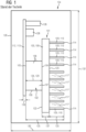
- FIG 1 shows a schematic sectional view of a known cooling device 101, which is integrated into a converter housing 126 of a converter 134.
- a semiconductor module 102 is connected to the base body 108 via its first cover surface 104.
- the semiconductor module 102 is also connected to a component carrier element 112, here a printed circuit board 113, via its second cover surface 105.
- the semiconductor module 102 forms a module space 107, which is determined by the first and second cover surfaces 104, 105 and the side surfaces 106.
- the component carrier element 112 / the circuit board 113 has further electronic components 128, which are arranged away from the cooling device 101, but are integrated with the component carrier element 112 / the circuit board 113 into the converter housing 126 of the converter 134.
- cooling elements 109 in the form of cooling fins 110 are formed, which protrude orthogonally from the base body 108.
- the cooling elements 109 and the second surface 125 of the base plate 108 of the heat sink 103 are surrounded by a cooling medium 117.
- the illustration of the converter housing 126 of the converter 134 shows a view of the converter housing 126, which reveals a housing width 130 and a housing height 132 of the converter housing 126.
- the housing width 130 of the converter housing 126 of the converter 124 is, as FIG 1 also evidently shows, is essentially determined by a cooling device width 135 of the cooling device 101.
- This cooling device width 135 sums up a module height 129 of the semiconductor module 102, a second thickness 137 of the base body 108 of the heat sink 103 and a maximum cooling element length 123 of the cooling elements 109, here the cooling fins 110.
- the module height 129 is determined by the cover surface distance 124 of the first cover surface 104 from the second cover surface 105 and the maximum cooling element length 123 is determined by a distance of the second surface 125 of the base body 108 from a cooling element end 114 assigned to the respective cooling element 109, which in each case faces away from the second surface 125 of the base body 108.
- the first thickness 136 of the component carrier element 112, here the circuit board 113, can be added to the cooling device width 135 in order to be able to make a comparison with the housing width 130 of the converter housing 126.
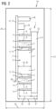
- FIG 2 a first schematic sectional view of a cooling device 1 according to the invention is shown, which is integrated into a converter housing 26 of a converter 34 according to the invention.
- a semiconductor module 2 is connected to the base body 8 via its first cover surface 4.
- the semiconductor module 2 is also connected to a component carrier element 12, here a printed circuit board 13, via its second cover surface 5.
- the semiconductor module 2 forms a module space 7, which is determined by the first and second cover surfaces 4, 5 and the side surfaces 6.
- the component carrier element 12 / the circuit board 13 has further electronic components 28, which are arranged away from the cooling device 1, but are integrated with the component carrier element 12 / the circuit board 13 in the converter housing 6 of the converter 4.
- Cooling elements 9 in the form of cooling fins 10 are also formed on the first surface 22 of the base body 8 of the heat sink 3, which here protrude orthogonally from the base body 8, whereby the semiconductor module 2 is embedded by the cooling elements 9.
- a cooling medium 17 flows around both the semiconductor module 2 and the cooling elements 9 and the first surface 22 of the base body 8 of the heat sink 3.
- the illustration of the converter housing 26 of the converter 34 shows a view of the converter housing 26, which reveals a housing width 30 and a housing height 32 of the converter housing 26.
- the housing width 30 of the converter housing 26 of the converter 24 is, as FIG 2 also evidently shows, essentially determined by a cooling device width 35 of the cooling device 1.
- This cooling device width 35 sums up a module height 29 of the semiconductor module 2 and a second thickness 37 of the base body 8 of the heat sink 3.
- the cooling elements 9 are smaller here than the module height 29 of the semiconductor module 2 with regard to their maximum cooling element length 23.
- the cooling element length 23 therefore does not exceed the module height 29 of the semiconductor module 2 and therefore does not influence the determined cooling device width 35 of the cooling device 1.
- the module height 29 is determined by the cover surface distance 24 of the first cover surface 4 from the second cover surface 5.
- the maximum cooling element length 23 of the cooling elements 9 is determined by a distance of the first surface 22 of the base body 8 from a cooling element end 14 assigned to the respective cooling element 9, which in each case faces away from the first surface 22 of the base body 8.
- the first thickness 36 of the component carrier element 12, here the circuit board 13, can be added to the cooling device width 35 in order to be able to make a comparison with the housing width 30 of the converter housing 26.
- a comparison of the cooling device width 35 of the cooling device 1 according to the invention from FIG 2 to the cooling device width 135 of the known cooling device 101 from FIG 1 also clearly shows that the cooling device width 35 of the cooling device 1 according to the invention FIG 2 significantly compared to the cooling device width 135 of the known cooling device 101 from FIG 1 is reduced.
- the housing width 30 of the converter housing 26 of the converter 34 according to the invention clearly compared to the housing width 130 of the converter housing 126 of the known converter 134, as in FIG 1 shown, can be reduced.
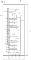
- FIG 3 a second schematic sectional view of the cooling device 1 according to the invention integrated into the converter housing 26 of the converter 34 according to the invention is shown FIG 2 shown.
- the second schematic sectional view from FIG 3 essentially corresponds to the first schematic sectional view from FIG 2 , thus FIG 3 analogous to FIG 2 , but with the difference that the cooling device 1 has a cooling element cover 15.
- This cooling element cover 15 is connected to the cooling elements 9, here the cooling fins 10, via their cooling element ends 14.
- the cooling element cover 15 also extends over the semiconductor module 2 and is here connected to the semiconductor module 2 via the second cover surface 5 of the semiconductor module 2.
- the semiconductor module 2 is connected at its second cover surface 5 only via two electrical vias 33 shown as an example to the component carrier element 12, here the printed circuit board 13
- the representation of the converter housing 26 of the converter 34 in FIG 3 shows a view of the converter housing 26, which reveals a housing width 30 and a housing height 32 of the converter housing 26.
- the housing width 30 of the converter housing 26 of the converter 24 is, as FIG 3 also evidently shows, is essentially determined by a cooling device width 35 of the cooling device 1.
- This cooling device width 35 sums up the module height 29 of the semiconductor module 2, the second thickness 37 of the base body 8 of the heat sink 3 and a third thickness 38 of the cooling element cover 15.
- the cooling elements 9 are here the same size as the module height 29 of the semiconductor module 2 with regard to their maximum cooling element length 23.
- the module height 29 is determined by the cover surface distance 24 of the first cover surface 4 from the second cover surface 5.
- the maximum cooling element length 23 of the cooling elements 9 is determined by a distance of the first surface 22 of the base body 8 from a cooling element end 14 assigned to the respective cooling element 9, which in each case faces away from the first surface 22 of the base body 8.
- the first thickness 36 of the component carrier element 12, here the circuit board 13, can be added to the cooling device width 35 in order to be able to make a comparison with the housing width 30 of the converter housing 26.
- a comparison of the cooling device width 35 of the cooling device 1 according to the invention from FIG 3 to the cooling device width 135 of the known cooling device 101 from FIG 1 clearly shows that the cooling device width 35 of the cooling device 1 according to the invention FIG 3 significantly compared to the cooling device width 135 of the known cooling device 101 from FIG 1 is reduced.
- the housing width 30 of the converter housing 26 of the converter 34 according to the invention clearly compared to the housing width 130 of the converter housing 126 of the known converter 134, as in FIG 1 shown, can be reduced.
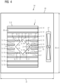
- FIG 4 shows a schematic detailed representation of the cooling device 1 according to the invention, integrated in the converter housing 26 of the converter 34 according to the invention according to FIG 2 and FIG 3 .
- the cooling device 1 is shown here in a side view. Cooling elements 9 in a combination of cooling fins 10 and pin fins 11 are formed on the first surface 22 of the base plate 8 of the heat sink 3. The semiconductor module 2 connected to the first surface 22 of the base plate 8 is embedded by the cooling elements 9.
- a first side surface 18 of the side surfaces 6 forms with the second side surface 19 of the side surfaces 6 a common side edge 20 which faces the flow direction 16, wherein the facing of the first to the second side surface 18,19 is determined by an edge angle 21.
- This edge angle 21 influences the flow direction 16 as the cooling medium 17 flows past the first and second side surfaces 18, 19 of the semiconductor module 2 and thus the cooling effect of the cooling medium 17 on the first and second side surfaces 18, 19 of the semiconductor module 2.
- a convection generator 27 for example a fan for the cooling medium 17, which is gaseous, or a pump for the cooling medium 17, which is liquid, generates a forced convection of the cooling medium 17 along the flow direction 16.
- the schematic detailed representation shows a specific view of the converter housing 26 of the converter 34, which reveals a housing depth 31 and a housing height 32 of the converter housing 26.
Landscapes
- Engineering & Computer Science (AREA)
- Microelectronics & Electronic Packaging (AREA)
- Physics & Mathematics (AREA)
- Thermal Sciences (AREA)
- Cooling Or The Like Of Electrical Apparatus (AREA)
- Cooling Or The Like Of Semiconductors Or Solid State Devices (AREA)
Description
Die Erfindung betrifft eine Kühlvorrichtung mit einem Halbleitermodul zur Kühlung des Halbleitermoduls und einen Umrichter mit der Kühlvorrichtung.The invention relates to a cooling device with a semiconductor module for cooling the semiconductor module and a converter with the cooling device.
In praktisch allen Anwendungsgebieten der Industrie und Energieerzeugung/Energieverteilung sind die Anforderungen an einen kompakteren Aufbau von elektrischen Geräten, in der Antriebstechnik an den kompakteren Aufbau von elektrischen Umrichtern, kaum zu ignorieren, wenn sich ein wirtschaftlicher und technischer Erfolg durch die Anbietung und den Einsatz dieser elektrischen Geräte einstellen soll.In practically all areas of application in industry and energy generation/distribution, the requirements for a more compact design of electrical devices, and in drive technology for a more compact design of electrical converters, can hardly be ignored if economic and technical success is to be achieved through the offer and use of these electrical devices.
So besteht beispielsweise für Umrichter bzgl. deren elektrischer Dimensionierung, deren spezialisierter Einsatzaufgaben oder auch deren örtlicher Einbaubegrenzungen der Bedarf an modularisierten und strukturierten Lösungen.For example, there is a need for modularized and structured solutions for converters with regard to their electrical dimensioning, their specialized application tasks or their local installation limitations.
So können beispielsweise Umrichter mehrere Umrichtermodule und Umrichtersysteme mehrere Umrichter aufweisen, die sich in ihrer Funktionalität und elektrischer Dimensionierung gleichen können, aber auch Unterschiede aufweisen können. Standardisierte Kopplungsmechanismen, mittels beispielweise Rückwandbussen, sollen und können derartige Umrichter bzw. Umrichtersysteme technisch und räumlich sehr nah zusammenbringen.For example, converters can have several converter modules and converter systems can have several converters, which can be similar in terms of their functionality and electrical dimensions, but can also have differences. Standardized coupling mechanisms, for example using backplane buses, should and can bring such converters or converter systems very close together in terms of technology and space.
Dies macht es jedoch notwendig, zumindest alle technisch relevanten Bauelemente des Umrichters möglichst noch kompakter an einem bzw. in einem Umrichter anzuordnen.However, this makes it necessary to arrange at least all technically relevant components of the converter as compactly as possible on or in one converter.
Ein Beispiel dafür zeigt die Siemens-Umrichterreihe SINAMICS S120 der Bauform Booksize. Wie der Name nahelegt, weist der Umrichter oder auch seine Umrichtermodule bzgl. des geometrischen bzw. anschaulichen Aufbaus eine Buchform auf. Die Höhe und die Tiefe der Bauform dieser Umrichterreihe sind aktuell im Wesentlichen fest vorgegeben, die Breite kann jedoch variieren. Demnach bietet die Breite Potential, den Bauraum weiter zu minimieren.An example of this is the Siemens SINAMICS S120 converter series in booksize format. As the name suggests, the converter or its converter modules have a geometric or clear structure in a book format. The height and depth of the design of this inverter series are currently essentially fixed, but the width can vary. The width therefore offers the potential to further minimize the installation space.
Baugruppen in Umrichtern, welche oftmals noch einen anteilig großen Bauraum erfordert, sind Kühlkörper bzw. Kühlvorrichtungen zur Entwärmung von elektrischen bzw. elektronischen Bauelementen in Kombination mit diesen Bauelementen.Components in converters, which often require a relatively large amount of installation space, are heat sinks or cooling devices for dissipating heat from electrical or electronic components in combination with these components.
Die minimale Breite der genannten Umrichterreihe wird hauptsächlich noch durch die Auslegung der Kühlvorrichtung mit dem Kühlkörper und das zur betrieblichen Entwärmung mit dem Kühlkörper verbundene Halbleitermodul bestimmt. Als Halbleitermodul wird in diesem Zusammenhang sowohl ein Halbleitermodul mit einem einzelnen Halbleiter aber auch ein Halbleitermodul in Form einer Brückenschaltung mit mehreren Halbleitern - wie beispielsweise in einer Sechspuls-Brückenschaltung (B6-Brücke) - verstanden. Typische Halbleiter sind als Leistungshalbleiter ausgebildete IGBTs (Insulated-Gate Bipolar Transistor) oder MOSFETs (Metal Oxide Semiconductor Field-Effect Transistor).The minimum width of the converter series mentioned is mainly determined by the design of the cooling device with the heat sink and the semiconductor module connected to the heat sink for operational heat dissipation. In this context, a semiconductor module is understood to be both a semiconductor module with a single semiconductor and a semiconductor module in the form of a bridge circuit with several semiconductors - such as in a six-pulse bridge circuit (B6 bridge). Typical semiconductors are IGBTs (Insulated-Gate Bipolar Transistor) or MOSFETs (Metal Oxide Semiconductor Field-Effect Transistor) designed as power semiconductors.
Die Dokumente
Die Dokumente
Derzeit bekannte Aufbautechnologien existierender Kühlvorrichtung erfordern einen aus Sicht der Hersteller wie auch der Anwender immer noch zu hohen Platzbedarf, um beispielsweise neue technische Einsatzgebiete mittels kleinerer, dezentral angeordneter Umrichter zu erschließen oder Umrichter bzw. Umrichtermodule feingranularer bzgl. ihrer Leistungsdaten und ihrer Funktionalität einzusetzen.Currently known construction technologies of existing cooling devices still require too much space from the point of view of both the manufacturer and the user, for example to open up new technical areas of application by means of smaller, decentrally arranged converters or converters or converter modules with a more fine-grained approach in terms of their performance data and functionality.
Der Erfindung liegt die Aufgabe zugrunde, eine Kühlvorrichtung zur Kühlung eines Halbeitermoduls und einen Umrichter mit der Kühlvorrichtung vorzuschlagen, welche gegenüber dem Stand der Technik einen geringeren Platzbedarf benötigen.The invention is based on the object of proposing a cooling device for cooling a semiconductor module and a converter with the cooling device, which require less space than the prior art.
Die Aufgabe wird durch eine Kühlvorrichtung mit den in Anspruch 1 angegebenen Merkmalen und durch einen Umrichter mit den in Anspruch 14 angegebenen Merkmalen gelöst.The object is achieved by a cooling device having the features specified in
Für die Lösung der Aufgabe wird eine Kühlvorrichtung mit einem Halbleitermodul und einem Kühlkörper zur Kühlung des Halbleitermoduls vorgeschlagen, wobei das Halbleitermodul eine erste und zweite Deckfläche und mehrere Seitenflächen aufweist, wobei die erste von der zweiten Deckfläche abgewandt ist, wobei zwischen den Deckflächen ein Modulraum des Halbleitermoduls ausgebildet ist, welcher von den Seitenflächen umschlossen ist, wobei der Kühlkörper einen Grundkörper aufweist, wobei an einer ersten Fläche des Grundkörpers von dem Grundkörper abstehende Kühlelemente ausgebildet sind, wobei das Halbleitermodul an der ersten Deckfläche mit der ersten Fläche des Grundkörpers verbunden ist und das Halbleitermodul zwischen zumindest einigen der Kühlelemente eingebettet ist.To achieve the object, a cooling device with a semiconductor module and a heat sink for cooling the semiconductor module is proposed, wherein the semiconductor module has a first and second cover surface and a plurality of side surfaces, wherein the first faces away from the second cover surface, wherein a module space of the semiconductor module is formed between the cover surfaces, which is enclosed by the side surfaces, wherein the heat sink has a base body, wherein cooling elements protruding from the base body are formed on a first surface of the base body, wherein the semiconductor module is connected to the first surface of the base body at the first cover surface and the semiconductor module is embedded between at least some of the cooling elements.
Eine Ausrichtung und Anordnung der Kühlelemente erfolgt der art, dass das zu entwärmende Halbleitermodul mit möglichst einer großen Fläche, insbesondere seiner Seitenflächen, in der Strömungsrichtung angeordnet ist und so von dem Kühlmedium erfindungsgemäß umströmt und entwärmt werden kann.The cooling elements are aligned and arranged in such a way that the semiconductor module to be cooled is arranged with as large an area as possible, in particular its side surfaces, in the flow direction and can thus be flowed around and cooled by the cooling medium according to the invention.
Zumindest eine erste und eine zweite Seitenfläche der Seitenflächen des Halbleitermoduls bilden eine gemeinsame Seitenkante aus und die gemeinsame Seitenkante der ersten und zweiten Seitenfläche ist der Strömungsrichtung zugewandt.At least a first and a second side surface of the side surfaces of the semiconductor module form a common side edge and the common side edge of the first and second side surfaces faces the flow direction.
An der Seitenkante kann sich das in Strömungsrichtung strömende Kühlmedium brechen, so dass es sich teilt und hier beispielhaft beide Seitenflächen des Halbleitermoduls in erfindungsgemäße Weise umströmen und entwärmen kann.At the side edge, the cooling medium flowing in the direction of flow can break so that it splits and can, for example, flow around and dissipate heat from both side surfaces of the semiconductor module in the manner according to the invention.
Durch die Einbettung des Halbleitermoduls zwischen den Kühlelementen verringert sich das Aufbauvolumen und damit der Platzbedarf des erfindungsgemäßen Aufbaus aus Kühlkörper, Kühlelementen und Halbleitermodul in vorteilhafter Weise gegenüber einem bekannten Aufbau, bei dem die Kühlelemente nicht auf der als Montagefläche des Halbleitermoduls ausgewiesenen ersten Fläche des Grundkörpers ausgebildet und somit nicht gemeinsam mit dem Halbleitermodul mittels dieser speziellen Aufbautopologie angeordnet sind.By embedding the semiconductor module between the cooling elements, the construction volume and thus the space requirement of the construction according to the invention comprising the heat sink, cooling elements and semiconductor module is reduced in an advantageous manner compared to a known construction in which the cooling elements are not formed on the first surface of the base body designated as the mounting surface of the semiconductor module and are therefore not arranged together with the semiconductor module by means of this special construction topology.
Unter dem Begriff Einbettung wird hier im räumlichen Sinne auch ein Umfassen, ein Umschließen, ein Umgeben oder ein Begrenzen des Halbleitermoduls insbesondere an seinen Seitenflächen durch die Kühlelemente verstanden. Ein so entstehender Einbettungsraum für das Halbleitermodul ist zumindest auch durch die erste Fläche des Grundkörpers des Kühlkörpers begrenzt.The term embedding is understood here in the spatial sense to mean enclosing, enclosing, surrounding or limiting the semiconductor module, particularly on its side surfaces, by the cooling elements. An embedding space for the semiconductor module created in this way is also limited at least by the first surface of the base body of the heat sink.
In dem gebildeten Modulraum des Halbleitermoduls kann ein einzelner Halbleiter oder mehrere Halbleiter, beispielsweise in Form einer B6-Brückenschaltung, angeordnet sein.A single semiconductor or several semiconductors, for example in the form of a B6 bridge circuit, can be arranged in the formed module space of the semiconductor module.
Die Anzahl der Seitenflächen, welche den Modulraum mit ausbilden, ist nicht begrenzt, wobei aber mindestens drei Seitenflächen vorgesehen sind.The number of side surfaces that form the modular space is not limited, but at least three side surfaces are provided.
Vorteilhafte Ausgestaltungsformen der Kondensatorvorrichtung sind in den abhängigen Ansprüchen angegeben.Advantageous embodiments of the capacitor device are specified in the dependent claims.
Bei einer ersten vorteilhaften Ausgestaltungsform der Kühlvorrichtung sind die Kühlelemente als Kühlrippen oder Pin Fins oder einer Kombination aus Kühlrippen und Pin Fins ausgebildet.In a first advantageous embodiment of the cooling device, the cooling elements are designed as cooling fins or pin fins or a combination of cooling fins and pin fins.
Der Begriff Pin Fin ist ein zwischenzeitlich im Zusammenhang mit Kühlkörpern technisch etablierter Begriff. Er kennzeichnet stiftartige Ausbuchtungen an Kühlkörpern, welche gegenüber herkömmlichen Kühlrippen in der Regel, als einzelner Pin Fin, kleiner und feingranularer auf einer Oberfläche eines Kühlkörpers verteilbar sind.The term pin fin is a term that has now become technically established in connection with heat sinks. It describes pin-like bulges on heat sinks, which, compared to conventional cooling fins, are usually smaller and can be distributed more finely on the surface of a heat sink as a single pin fin.
Mittels herkömmlicher Kühlrippen kann ein Konvektionsstrom im Allgemeinen vorteilhaft kanalartig in eine Richtung über den Kühlkörper geleitet werden, wobei Pin Fins mittels ihrer feingranularen Anordnungsmöglichkeit einen Konvektionsstrom an spezifischen Stellen auch vorteilhaft ausdünnen oder, unter Erzeugung örtlicher Wirbel, verstärken können.By means of conventional cooling fins, a convection current can generally be advantageously channeled in one direction over the heat sink, whereby pin fins, thanks to their fine-grained arrangement option, can also advantageously thin out a convection current at specific locations or, by generating local vortices, strengthen it.
Je nach Anforderung an beispielsweise die Bauform des zu entwärmenden Halbleitermoduls können Kühlrippen, Pin Fins oder eine Kombination aus beiden Kühlelementen effektiver sein.Depending on the requirements, for example the design of the semiconductor module to be cooled, cooling fins, pin fins or a combination of both cooling elements may be more effective.
Bei einer weiteren vorteilhaften Ausgestaltungsform der Kühlvorrichtung ist das Halbleitermodul an seiner zweiten Deckfläche mit einem Bauteilträgerelement, insbesondere einer Leiterplatte, verbunden.In a further advantageous embodiment of the cooling device, the semiconductor module is connected at its second cover surface to a component carrier element, in particular a printed circuit board.
Eine elektrische Anbindung des Halbleitermoduls erfolgt meist über das Bauteilträgerelement, bevorzugt die Leiterplatte.The semiconductor module is usually electrically connected via the component carrier element, preferably the circuit board.
Die vorteilhafte Anordnung des Halbleitermoduls zwischen der ersten Fläche des Grundkörpers und dem Bauteilträgerelement reduziert den zur Anbindung des Halbleitermoduls an den Kühlkörper erforderlichen Platzbedarf weiter in vorteilhafter Weise.The advantageous arrangement of the semiconductor module between the first surface of the base body and the component carrier element further advantageously reduces the space required to connect the semiconductor module to the heat sink.
Als Bauteilträgerelement kann auch eine Stromschiene oder ein anderer elektrische Leiter eingesetzt werden, an der das dann Halbleitermodul befestigt ist.A busbar or another electrical conductor can also be used as a component carrier element, to which the semiconductor module is then attached.
Bei einer weiteren vorteilhaften Ausgestaltungsform der Kühlvorrichtung weist die Kühlvorrichtung eine Kühlelementabdeckung auf, wobei die Kühlelemente jeweils einen von dem Grundkörper abgewandten Kühlelementabschluss ausbilden und zumindest einige der Kühlelemente an deren Kühlelementabschlusses mit der Kühlelementabdeckung verbunden sindIn a further advantageous embodiment of the cooling device, the cooling device has a cooling element cover, wherein the cooling elements each form a cooling element end facing away from the base body and at least some of the cooling elements are connected to the cooling element cover at their cooling element end
Mittels der Kühlelementabdeckung können gerichtete Kühlkanäle besser gegen die Umgebung der Kühlvorrichtung abgeschottet werden, wobei eine Konvektion zielgerichteter zumindest an den Seitenflächen des Halbleitermoduls vorbeiführbar und somit das Halbleitermodul vorteilhaft entwärmbar ist.By means of the cooling element cover, directed cooling channels can be better sealed off from the surroundings of the cooling device, whereby convection can be guided more specifically past at least the side surfaces of the semiconductor module and thus the semiconductor module can be advantageously cooled.
Bei einer weiteren vorteilhaften Ausgestaltungsform der Kühlvorrichtung ist die Kühlelementabdeckung aus einem gleichen metallischen Material ausgebildet, wie der Grundkörper des Kühlkörper und/oder die Kühlelemente.In a further advantageous embodiment of the cooling device, the cooling element cover is made of the same metallic material as the base body of the heat sink and/or the cooling elements.
Die Kühlelementabdeckung weist damit ebenfalls die aufgrund der metallischen Ausprägung üblicherweise sehr guten thermischen Kühleigenschaften des Grundkörpers und/oder der Kühlelemente auf, so dass eine verbesserte Abführung der im Betrieb des Halbleitermoduls erzeugten Verlustwärme an die Umgebung der Kühlvorrichtung vorteilhaft durchführbar ist.The cooling element cover thus also has the usually very good thermal cooling properties of the base body and/or the cooling elements due to the metallic nature, so that an improved dissipation of the waste heat generated during operation of the semiconductor module to the environment of the cooling device can advantageously be carried out.
Bei einer weiteren vorteilhaften Ausgestaltungsform der Kühlvorrichtung ist der Kühlkörper monolithisch aus dem Grundkörper, den Kühlelementen und der Kühlelementabdeckung ausgebildet.In a further advantageous embodiment of the cooling device, the heat sink is formed monolithically from the base body, the cooling elements and the cooling element cover.
Der derart vorgestellte monolithische Aufbau ermöglicht eine kompakt und industriell kostengünstig herstellbare Kühlvorrichtung.The monolithic structure presented in this way enables a cooling device that can be manufactured compactly and cost-effectively on an industrial scale.
Da das Halbleitermodul zwischen den Kühlelementen eingebettet und mit der ersten Fläche der Grundplatte verbunden ist, kann bei der Herstellung der Kühlvorrichtung eine Aussparung in der Abdeckplatte zur Einbringung des Halbleitermoduls vorgesehen sein.Since the semiconductor module is embedded between the cooling elements and connected to the first surface of the base plate, a recess can be provided in the cover plate for introducing the semiconductor module during manufacture of the cooling device.
Bei einer weiteren vorteilhaften Ausgestaltungsform der Kühlvorrichtung ist die Kühlelementabdeckung als Bauteilträgerelement, insbesondere als Leiterplatte, ausgebildet.In a further advantageous embodiment of the cooling device, the cooling element cover is designed as a component carrier element, in particular as a printed circuit board.
Es ist eine Grundfunktionalität des Bauteilträgerelements / speziell der Leiterplatte, elektronischen und elektrotechnischen Bauelementen, wie dem des Halbleitermoduls, eine elektrische und mechanische Anbindung innerhalb eines elektrischen Gerätes, wie dem des Umrichters, zu geben. Demnach ist das Bauteilträgerelement / die Leiterplatte im Allgemeinen systemimmanenter Bestandteil von Umrichter. Die Kombination mit einer weiteren Funktion, der der Abdeckung der Kühlelemente, verringert vorteilhaft den Platzbedarf für die Kühlvorrichtung und kann helfen, die Abmaße und somit das Bauraumvolumen von Umrichtern vorteilhaft zu reduzieren.A basic functionality of the component carrier element / especially the circuit board is to provide electronic and electrotechnical components, such as the semiconductor module, with an electrical and mechanical connection within an electrical device, such as the converter. Accordingly, the component carrier element / circuit board is generally an inherent part of the converter. The combination with another function, that of covering the cooling elements, advantageously reduces the space required for the cooling device and can help to advantageously reduce the dimensions and thus the installation space volume of converters.
Die Verwendung des Bauteilträgerelements / der Leiterplatte als Kühlelementabdeckung kann es erforderlich machen, dass eine elektrische Isolation des Bauteilträgerelements / der Leiterplatte gegenüber den Kühlelementen erfolgen muss.The use of the component carrier element / circuit board as a cooling element cover may make it necessary to electrically isolate the component carrier element / circuit board from the cooling elements.
Bei einer weiteren vorteilhaften Ausgestaltungsform der Kühlvorrichtung können die Kühlelemente und die Seitenflächen des Halbleitermoduls in einer Strömungsrichtung entlang des Grundkörpers mittels eines Kühlmediums umströmt werden.In a further advantageous embodiment of the cooling device, the cooling elements and the side surfaces of the semiconductor module can be flowed around in a flow direction along the base body by means of a cooling medium.
Bei einer weiteren vorteilhaften Ausgestaltungsform der Kühlvorrichtung ist das Kühlmedium flüssig, insbesondere Wasser, oder gasförmig, insbesondere Luft.In a further advantageous embodiment of the cooling device, the cooling medium is liquid, in particular water, or gaseous, in particular air.
Bei einer weiteren vorteilhaften Ausgestaltungsform der Kühlvorrichtung weist ein Kantenwinkel an der gemeinsamen Seitenkante zwischen der ersten und zweiten Seitenfläche einen Wert in einem Winkelbereich von 30° bis 60°, insbesondere von 45°, auf.In a further advantageous embodiment of the cooling device, an edge angle at the common side edge between the first and second side surface has a value in an angular range of 30° to 60°, in particular of 45°.
Es zeigt sich, dass der Kantenwinkel im Bereich von 30° bis 60° das Umströmen der Seitenflächen besonders effektiv macht, da es einerseits nicht zum Stau des Kühlmediums an den Seitenflächen kommt, andererseits das Kühlmedium nicht zu schnell an den Seitenflächen vorbeiströmt, ohne die Verlustwärme ausreichend aufnehmen und vom Halbleitermodul wegtransportieren zu können. Ein bevorzugter Wert für den Kantenwinkel sind 45°, was bei einem vierseitigen, rechteckigen Halbleitermodul baulich vorgegeben ist.It turns out that the edge angle in the range of 30° to 60° makes the flow around the side surfaces particularly effective, since on the one hand the cooling medium does not accumulate on the side surfaces, and on the other hand the cooling medium does not flow past the side surfaces too quickly without the heat loss to be able to absorb and transport the material sufficiently away from the semiconductor module. A preferred value for the edge angle is 45°, which is structurally specified for a four-sided, rectangular semiconductor module.
Bei einer weiteren vorteilhaften Ausgestaltungsform der Kühlvorrichtung wird eine maximale Kühlelementlänge der an der ersten Fläche des Grundkörpers ausgebildeten Kühlelemente, beginnend von der ersten Fläche des Grundkörpers bis zum Kühlelementabschluss des jeweiligen Kühlelements, durch einen Deckflächenabstand zwischen der ersten Deckfläche und der zweiten Deckfläche des Halbleitermoduls begrenzt.In a further advantageous embodiment of the cooling device, a maximum cooling element length of the cooling elements formed on the first surface of the base body, starting from the first surface of the base body to the cooling element end of the respective cooling element, is limited by a cover surface distance between the first cover surface and the second cover surface of the semiconductor module.
Eines der bestimmenden Bauelemente für eine Gesamtbreite der Kühlvorrichtung ist das Halbleitermodul. Da es ein meist am Markt in seinen spezifischen Abmaßen erhältliches und damit vorgegebenes Bauelement ist, müssen sich insbesondere die Kühlelemente an den vorgegebenen Abmaßen des Halbleitermoduls orientieren.One of the components that determine the overall width of the cooling device is the semiconductor module. Since it is a component that is usually available on the market in its specific dimensions and is therefore predetermined, the cooling elements in particular must be based on the specified dimensions of the semiconductor module.
Die hier benannten Deckflächen stellen, neben den Seitenflächen, die äußeren Abmaße des Halbleitermoduls dar, wobei elektrische Anschlüsse für die Ankontaktierung des Halbleitermoduls oder auch mechanische Befestigungsmittel aus dieser Betrachtung herausgenommen werden können.The cover surfaces mentioned here, in addition to the side surfaces, represent the external dimensions of the semiconductor module, whereby electrical connections for contacting the semiconductor module or mechanical fastening means can be excluded from this consideration.
Bei einer weiteren vorteilhaften Ausgestaltungsform der Kühlvorrichtung ist eine von der ersten Fläche des Grundkörpers abgewandte zweite Fläche des Grundkörpers frei von Kühlelementen.In a further advantageous embodiment of the cooling device, a second surface of the base body facing away from the first surface of the base body is free of cooling elements.
Auf eine Ausbildung von Kühlelementen an der zweiten Fläche des Grundkörpers des Kühlkörpers wird vorteilhaft verzichtet, da so die Reduzierung der Baugröße und damit des Bauvolumens der Kühlvorrichtung besonders wirksam ist.It is advantageous to dispense with the formation of cooling elements on the second surface of the base body of the heat sink, since this makes the reduction of the size and thus the volume of the cooling device particularly effective.
Für die Lösung der Aufgabe wird weiterhin ein Umrichter mit der erfindungsgemäßen Kühlvorrichtung und einem Umrichtergehäuse vorgeschlagen, wobei die Kühlvorrichtung in das Umrichtergehäuse integriert ist.To solve the problem, a converter with the cooling device according to the invention and a converter housing proposed, whereby the cooling device is integrated into the converter housing.
Der Einsatz der erfindungsgemäßen Kühlvorrichtung im Umrichter, mit einer Integration in das Umrichtergehäuse, reduziert maßgeblich insbesondere die Bauraumbreite des Umrichtergehäuses und damit des Umrichters.The use of the cooling device according to the invention in the converter, with integration into the converter housing, significantly reduces in particular the installation space width of the converter housing and thus of the converter.
Bei einer vorteilhaften Ausgestaltungsform des Umrichters ist eine erzwungene Konvektion des Kühlmediums durch einen Konvektionserzeuger erzeugbar.In an advantageous embodiment of the converter, a forced convection of the cooling medium can be generated by a convection generator.
Die erzwungene Konvektion forciert die Entwärmung des Halbleitermoduls, indem das Kühlmedium gezielter, schneller und in größerer Volumenzahl zu dem zu entwärmenden Halbleitermodul transportiert werden kann und, unter Aufnahme der im Betrieb entstehenden Verlustwärme des Halbleitermoduls, von diesem abtransportiert werden kann.Forced convection forces the cooling of the semiconductor module by allowing the cooling medium to be transported more precisely, more quickly and in larger volumes to the semiconductor module to be cooled and to be transported away from it by absorbing the heat loss generated by the semiconductor module during operation.
Die oben beschriebenen Eigenschaften, Merkmale und Vorteile dieser Erfindung sowie die Art und Weise, wie diese erreicht werden, werden klarer und deutlicher verständlich im Zusammenhang mit der folgenden Beschreibung der Ausführungsbeispiele, die im Zusammenhang mit den Figuren näher erläutert werden. Es zeigt:
- FIG 1
- eine schematische Darstellung als Schnitt durch eine bekannte Kühlvorrichtung, integriert in ein Umrichtergehäuse eines Umrichters,
- FIG 2
- eine erste schematische Darstellung als Schnitt durch eine erfindungsgemäße Kühlvorrichtung, welche in ein Umrichtergehäuse eines erfindungsgemäßen Umrichters integriert ist,
- FIG 3
- eine zweite schematische Darstellung als Schnitt durch die in das Umrichtergehäuse des erfindungsgemäßen Umrichters integrierte erfindungsgemäße Kühlvorrichtung nach
FIG 2 und - FIG 4
- eine schematische Detaildarstellung der erfindungsgemäßen Kühlvorrichtung, integriert in das Umrichtergehäuse des erfindungsgemäßen Umrichters nach
FIG 2 undFIG 3 .
- FIG 1
- a schematic representation as a section through a known cooling device, integrated in a converter housing of a converter,
- FIG 2
- a first schematic representation as a section through a cooling device according to the invention, which is integrated into a converter housing of a converter according to the invention,
- FIG 3
- a second schematic representation as a section through the in the converter housing of the inventive Inverter integrated cooling device according to the invention
FIG 2 and - FIG 4
- a schematic detailed representation of the cooling device according to the invention, integrated into the converter housing of the converter according to the invention according to
FIG 2 andFIG 3 .
Die
An einer ersten Fläche 122 eines Grundkörpers 108 eines Kühlkörpers 103 ist ein Halbleitermodul 102 über seine erste Deckfläche 104 mit dem Grundkörper 108 verbunden. Das Halbleitermodul 102 ist darüber hinaus über seine zweite Deckfläche 105 mit einem Bauteilträgerelement 112, hier einer Leiterplatte 113, verbunden.On a
Das Halbleitermodul 102 bildet einen Modulraum 107 aus, welcher durch die erste und zweite Deckfläche 104,105 und die Seitenflächen 106 bestimmt ist.The
Das Bauteilträgerelement 112 / die Leiterplatte 113 weist weitere elektronische Bauelemente 128 auf, welche abseits der Kühlvorrichtung 101 angeordnet, aber mit dem Bauteilträgerelement 112 / der Leiterplatte 113 in das Umrichtergehäuse 126 des Umrichters 134 integriert sind.The component carrier element 112 / the circuit board 113 has further
Auf einer zweiten Fläche 125 des Grundkörpers 108 des Kühlkörpers 103, welche von der ersten Fläche 104 des Grundkörpers 108 abgewandt ist, sind Kühlelemente 109 in Form von Kühlrippen 110 ausgebildet, welche von dem Grundkörper 108 hier orthogonal abstehen. Die Kühlelemente 109 sowie die zweite Fläche 125 der Grundplatte 108 des Kühlkörpers 103 sind von einem Kühlmedium 117 umströmt.On a
Die Darstellung des Umrichtergehäuses 126 des Umrichters 134 zeigt eine Sicht auf das Umrichtergehäuse 126, welche eine Gehäusebreite 130 und eine Gehäusehöhe 132 des Umrichtergehäuses 126 erkennen lässt.The illustration of the
Die Gehäusebreite 130 des Umrichtergehäuses 126 des Umrichters 124 wird, wie
Diese Kühlvorrichtungsbreite 135 summiert eine Modulhöhe 129 des Halbleitermoduls 102, eine zweiten Dicke 137 des Grundkörpers 108 des Kühlkörpers 103 und eine maximale Kühlelementlänge 123 der Kühlelemente 109, hier der Kühlrippen 110.This
Die Modulhöhe 129 bestimmt sich dabei durch den Deckflächenabstand 124 der ersten Deckfläche 104 von der zweiten Deckfläche 105 und die maximale Kühlelementlänge 123 bestimmt sich durch einen Abstand der zweiten Fläche 125 des Grundkörpers 108 von einem dem jeweiligen Kühlelement 109 zugeordneten Kühlelementabschluss 114, welcher jeweils von der zweiten Fläche 125 des Grundkörpers 108 abgewandt ist.The module height 129 is determined by the cover surface distance 124 of the
Zu der Kühlvorrichtungsbreite 135 kann noch die erste Dicke 136 des Bauteilträgerelements 112, hier der Leiterplatte 113 hinzugezählt werden, um einen Vergleich mit der Gehäusebreite 130 des Umrichtergehäuses 126 herstellen zu können.The
Mit
An einer ersten Fläche 22 eines Grundkörpers 8 eines Kühlkörpers 3 ist ein Halbleitermodul 2 über seine erste Deckfläche 4 mit dem Grundkörper 8 verbunden. Das Halbleitermodul 2 ist darüber hinaus über seine zweite Deckfläche 5 mit einem Bauteilträgerelement 12, hier einer Leiterplatte 13, verbunden.On a
Das Halbleitermodul 2 bildet einen Modulraum 7 aus, welcher durch die erste und zweite Deckfläche 4,5 und die Seitenflächen 6 bestimmt ist.The
Das Bauteilträgerelement 12 / die Leiterplatte 13 weist weitere elektronische Bauelemente 28 auf, welche abseits der Kühlvorrichtung 1 angeordnet, aber mit dem Bauteilträgerelement 12 / der Leiterplatte 13 in das Umrichtergehäuse 6 des Umrichters 4 integriert sind.The component carrier element 12 / the circuit board 13 has further
Ebenfalls an der ersten Fläche 22 des Grundkörpers 8 des Kühlkörpers 3 sind Kühlelemente 9 in Form von Kühlrippen 10 ausgebildet, welche von dem Grundkörper 8 hier orthogonal abstehen, wodurch das Halbleitermodul 2 von den Kühlelementen 9 eingebettet wird.Cooling elements 9 in the form of cooling fins 10 are also formed on the
Sowohl das Halbleitermodul 2 wie auch die Kühlelemente 9 und die erste Fläche 22 des Grundkörpers 8 des Kühlkörpers 3 sind von einem Kühlmedium 17 umströmt.A cooling
Auf einer zweiten Fläche 25 des Grundkörpers 8 des Kühlkörpers 3, welche von der ersten Fläche 22 des Grundkörpers 8 abgewandt ist, sind keine Kühlelemente ausgebildet oder anderweitig Bauelemente angebracht.On a
Die Darstellung des Umrichtergehäuses 26 des Umrichters 34 zeigt eine Sicht auf das Umrichtergehäuse 26, welche eine Gehäusebreite 30 und eine Gehäusehöhe 32 des Umrichtergehäuses 26 erkennen lässt.The illustration of the
Die Gehäusebreite 30 des Umrichtergehäuses 26 des Umrichters 24 wird, wie
Diese Kühlvorrichtungsbreite 35 summiert eine Modulhöhe 29 des Halbleitermoduls 2 und eine zweiten Dicke 37 des Grundkörpers 8 des Kühlkörpers 3. Die Kühlelemente 9 sind bzgl. ihrer maximalen Kühlelementlänge 23 hier kleiner als die Modulhöhe 29 des Halbleitermoduls 2. Die Kühlelementlänge 23 geht somit nicht über die Modulhöhe 29 des Halbleitermoduls 2 hinaus und beeinflusst demnach auch nicht die ermittelte Kühlvorrichtungsbreite 35 der Kühlvorrichtung 1.This
Die Modulhöhe 29 bestimmt sich dabei durch den Deckflächenabstand 24 der ersten Deckfläche 4 von der zweiten Deckfläche 5. Die maximale Kühlelementlänge 23 der Kühlelemente 9 bestimmt sich durch einen Abstand der ersten Fläche 22 des Grundkörpers 8 von einem dem jeweiligen Kühlelement 9 zugeordneten Kühlelementabschluss 14, welcher jeweils von der ersten Fläche 22 des Grundkörpers 8 abgewandt ist.The module height 29 is determined by the cover surface distance 24 of the
Zu der Kühlvorrichtungsbreite 35 kann noch die erste Dicke 36 des Bauteilträgerelements 12, hier der Leiterplatte 13, hinzugezählt werden, um einen Vergleich mit der Gehäusebreite 30 des Umrichtergehäuses 26 herstellen zu können.The
Ein Vergleich der Kühlvorrichtungsbreite 35 der erfindungsgemäßen Kühlvorrichtung 1 aus
Somit kann die Gehäusebreite 30 des Umrichtergehäuses 26 des erfindungsgemäßen Umrichters 34, wie in
Mittels
Die zweite schematische Schnittdarstellung aus
Diese Kühlelementabdeckung 15 ist mit den Kühlelementen 9, hier den Kühlrippen 10, über deren Kühlelementabschlüsse 14 verbunden. Die Kühlelementabdeckung 15 reicht in diesem Anwendungsbeispiel auch über das Halbleitermodul 2 und ist hier über die zweite Deckfläche 5 des Halbleitermoduls 2 mit dem Halbleitermodul 2 verbunden.This
Im Gegensatz zu
Auch die Darstellung des Umrichtergehäuses 26 des Umrichters 34 in
Die Gehäusebreite 30 des Umrichtergehäuses 26 des Umrichters 24 wird, wie
Diese Kühlvorrichtungsbreite 35 summiert die Modulhöhe 29 des Halbleitermoduls 2, die zweiten Dicke 37 des Grundkörpers 8 des Kühlkörpers 3 und eine dritte Dicke 38 der Kühlelementabdeckung 15. Die Kühlelemente 9 sind hier bzgl. ihrer maximalen Kühlelementlänge 23 gleich groß wie die Modulhöhe 29 des Halbleitermoduls 2.This
Die Modulhöhe 29 bestimmt sich dabei durch den Deckflächenabstand 24 der ersten Deckfläche 4 von der zweiten Deckfläche 5. Die maximale Kühlelementlänge 23 der Kühlelemente 9 bestimmt sich durch einen Abstand der ersten Fläche 22 des Grundkörpers 8 von einem dem jeweiligen Kühlelement 9 zugeordneten Kühlelementabschluss 14, welcher jeweils von der ersten Fläche 22 des Grundkörpers 8 abgewandt ist.The module height 29 is determined by the cover surface distance 24 of the
Zu der Kühlvorrichtungsbreite 35 kann noch die erste Dicke 36 des Bauteilträgerelements 12, hier der Leiterplatte 13, hinzugezählt werden, um einen Vergleich mit der Gehäusebreite 30 des Umrichtergehäuses 26 herstellen zu können.The
Auch ein Vergleich der Kühlvorrichtungsbreite 35 der erfindungsgemäßen Kühlvorrichtung 1 aus
Somit kann auch die Gehäusebreite 30 des Umrichtergehäuses 26 des erfindungsgemäßen Umrichters 34, wie in
Die
Die Kühlvorrichtung 1 ist hier in einer seitlichen Ansicht dargestellt. An der ersten Fläche 22 der Grundplatte 8 des Kühlkörpers 3 sind Kühlelemente 9 in einer Kombination aus Kühlrippen 10 und Pin Fins 11 ausgebildet. Das mit der ersten Fläche 22 der Grundplatte 8 verbundene Halbleitermodul 2 ist von den Kühlelementen 9 eingebettet.The
Ein durch die Kühlelemente 9 in einer Strömungsrichtung 16 strömendes Kühlmedium 17 umströmt die Kühlelement 9 sowie das Halbleitermodul 2, insbesondere dessen Seitenflächen 6.A cooling
Eine erste Seitenfläche 18 der Seitenflächen 6 bildet mit der zweiten Seitenfläche 19 der Seitenflächen 6 eine gemeinsame Seitenkante 20 aus, welche der Strömungsrichtung 16 zugewandt ist, wobei die Zuwendung der ersten zur zweiten Seitenfläche 18,19 durch einen Kantenwinkel 21 bestimmt wird.A first side surface 18 of the side surfaces 6 forms with the second side surface 19 of the side surfaces 6 a
Dieser Kantenwinkel 21 beeinflusst die Strömungsrichtung 16 beim Vorbeiströmen des Kühlmediums 17 an der ersten und zweiten Seitenfläche 18,19 des Halbleitermoduls 2 und damit die entwärmende Wirkung des Kühlmediums 17 an der ersten und zweiten Seitenfläche 18,19 des Halbleitermoduls 2.This
Ein Konvektionserzeuger 27, beispielsweise ein Ventilator für das Kühlmedien 17, welches gasförmige ist, oder eine Pumpe für das Kühlmedium 17, welches flüssig ist, erzeugt eine zwangsgeführte Konvektion des Kühlmediums 17 entlang der Strömungsrichtung 16.A convection generator 27, for example a fan for the cooling
Die schematische Detaildarstellung zeigt eine spezifische Sicht auf das Umrichtergehäuse 26 des Umrichters 34, welche eine Gehäusetiefe 31 und eine Gehäusehöhe 32 des Umrichtergehäuses 26 erkennen lässt.The schematic detailed representation shows a specific view of the
Claims (13)
- Cooling apparatus (1) having a semiconductor module (2) and a heat sink (3) for cooling the semiconductor module (2), wherein- the semiconductor module (2) has a first and second cover face (4,5) and a plurality of side faces (6),- the first cover face (4) faces away from the second cover face (5),- a module space (7) of the semiconductor module (2) is formed between the cover faces (4,5), said module space being enclosed by the side faces (6),- the heat sink (3) has a base body (8),- cooling elements (9) are formed on a first face (22) of the base body (8) and said cooling elements project from the base body (8),- the semiconductor module (2) is connected to the first face (22) of the base body (8) at the first cover face (4),- the semiconductor module (2) is embedded between at least some of the cooling elements (9),- a cooling medium (17) can flow around the cooling elements (9) and the side faces (6) of the semiconductor module (2) in a flow direction (16) along the base body (8) and the cooling apparatus is characterised in that- at least a first and a second side face (18, 19) of the side faces (6) of the semiconductor module (2) form a common side edge (20) and the common side edge (20) of the first and second side face (18,19) faces the flow direction (16).
- Cooling apparatus (1) according to claim 1, wherein the cooling elements (9) are formed as cooling fins (10) or as pin fins (11) or a combination of cooling fins (10) and pin fins (11) .
- Cooling apparatus (1) according to one of claims 1 or 2, wherein the semiconductor module (2) is connected at its second cover face (5) to a component support element (12), in particular a printed circuit board (13), or to a cooling element cover (15).
- Cooling apparatus (1) according to claim 3, wherein the cooling elements (9) each form a cooling element end (14) that faces away from the base body (8) and at least some of the cooling elements (9) are connected at their cooling element end (14) to the cooling element cover (15).
- Cooling apparatus (1) according to claim 3 or 4, wherein the cooling element cover (15) is made of the same metal material as the base body (8) of the heat sink (3) and/or the cooling elements (9).
- Cooling apparatus (1) according to claim 5, wherein the heat sink (3) is monolithically formed from the base body (8), the cooling elements (9) and the cooling element cover (15).
- Cooling apparatus (1) according to claim 3 or 4, wherein the cooling element cover (15) is formed as a component support element (12), in particular as a printed circuit board (13) .
- Cooling apparatus (1) according to one of the preceding claims, wherein the cooling medium (17) is liquid, in particular water, or gaseous, in particular air.
- Cooling apparatus (1) according to one of the preceding claims, wherein an edge angle (21) at the common side edge (20) between the first and second side face (18,19) has an angle value in an angular range of 30° to 60°, in particular 45°.
- Cooling apparatus (1) according to one of the preceding claims, wherein a maximum cooling element length (23) of the cooling elements (9) that are formed on the first face (22) of the base body (8), starting from the first face (22) of the base body (8) to the cooling element end (14) of the respective cooling element (9), is limited by a cover face distance (24), which determines a module height (29) of the semiconductor module (2), between the first cover face (4) and the second cover face (5) of the semiconductor module (2).
- Cooling apparatus (1) according to one of the preceding claims, wherein cooling elements are not formed on a second face (25) of the base body (8), said second face facing away from the first face (22) of the base body (8).
- Converter (34) having a cooling apparatus (1), according to one of claims 1 to 11, and a converter housing (26), wherein the cooling apparatus (1) is integrated in the converter housing (26).
- Converter (34) according to claim 12, wherein forced convection of the cooling medium (17) can be generated by a convection generator (27).
Applications Claiming Priority (2)
| Application Number | Priority Date | Filing Date | Title |
|---|---|---|---|
| EP21166370.3A EP4068923A1 (en) | 2021-03-31 | 2021-03-31 | Cooling device for cooling a semiconductor module and converter with the cooling device |
| PCT/EP2022/053770 WO2022207179A1 (en) | 2021-03-31 | 2022-02-16 | Cooling device for cooling a semiconductor module and converter with the cooling device |
Publications (3)
| Publication Number | Publication Date |
|---|---|
| EP4268552A1 EP4268552A1 (en) | 2023-11-01 |
| EP4268552B1 true EP4268552B1 (en) | 2024-11-20 |
| EP4268552C0 EP4268552C0 (en) | 2024-11-20 |
Family
ID=75339588
Family Applications (2)
| Application Number | Title | Priority Date | Filing Date |
|---|---|---|---|
| EP21166370.3A Withdrawn EP4068923A1 (en) | 2021-03-31 | 2021-03-31 | Cooling device for cooling a semiconductor module and converter with the cooling device |
| EP22706045.6A Active EP4268552B1 (en) | 2021-03-31 | 2022-02-16 | Cooling device for cooling a semiconductor module and converter with the cooling device |
Family Applications Before (1)
| Application Number | Title | Priority Date | Filing Date |
|---|---|---|---|
| EP21166370.3A Withdrawn EP4068923A1 (en) | 2021-03-31 | 2021-03-31 | Cooling device for cooling a semiconductor module and converter with the cooling device |
Country Status (4)
| Country | Link |
|---|---|
| US (1) | US20240188254A1 (en) |
| EP (2) | EP4068923A1 (en) |
| CN (1) | CN117204129A (en) |
| WO (1) | WO2022207179A1 (en) |
Families Citing this family (1)
| Publication number | Priority date | Publication date | Assignee | Title |
|---|---|---|---|---|
| DE102023202803B3 (en) * | 2023-03-28 | 2024-06-27 | Siemens Aktiengesellschaft | Electronic arrangement |
Family Cites Families (7)
| Publication number | Priority date | Publication date | Assignee | Title |
|---|---|---|---|---|
| US4027206A (en) * | 1975-01-27 | 1977-05-31 | L. H. Research | Electronic cooling chassis |
| KR20110041014A (en) * | 2009-10-15 | 2011-04-21 | 이재오 | Heat sink manufacturing method using synthetic resin |
| GB2502148B (en) * | 2012-05-18 | 2015-04-29 | Control Tech Ltd | Printed circuit board heatsink mounting |
| JP2018186143A (en) * | 2017-04-25 | 2018-11-22 | オムロンオートモーティブエレクトロニクス株式会社 | Circuit board module, electronic device |
| EP3416467B1 (en) * | 2017-06-13 | 2022-05-04 | ABB Schweiz AG | Heat exchanger structure for a rack assembly |
| CN108966482A (en) * | 2018-07-16 | 2018-12-07 | 珠海格力电器股份有限公司 | Power ware heat radiation structure |
| CN211377343U (en) * | 2020-03-04 | 2020-08-28 | Abb瑞士股份有限公司 | Heat radiator |
-
2021
- 2021-03-31 EP EP21166370.3A patent/EP4068923A1/en not_active Withdrawn
-
2022
- 2022-02-16 US US18/285,058 patent/US20240188254A1/en active Pending
- 2022-02-16 CN CN202280026564.5A patent/CN117204129A/en active Pending
- 2022-02-16 WO PCT/EP2022/053770 patent/WO2022207179A1/en not_active Ceased
- 2022-02-16 EP EP22706045.6A patent/EP4268552B1/en active Active
Also Published As
| Publication number | Publication date |
|---|---|
| CN117204129A (en) | 2023-12-08 |
| EP4068923A1 (en) | 2022-10-05 |
| EP4268552A1 (en) | 2023-11-01 |
| WO2022207179A1 (en) | 2022-10-06 |
| EP4268552C0 (en) | 2024-11-20 |
| US20240188254A1 (en) | 2024-06-06 |
Similar Documents
| Publication | Publication Date | Title |
|---|---|---|
| EP1430758B1 (en) | Electrical circuit arrangement comprised of a number of electrically interconnected circuit components | |
| EP1848260B1 (en) | Inverter | |
| EP2114113B1 (en) | Printed Circuit Board and corresponding production method | |
| EP3361836A1 (en) | Low inductance half-bridge configuration | |
| DE102013222148A1 (en) | Coldplate for use with electronic components i.e. MOSFET of auxiliary power module in e.g. electric vehicle, has portions defining manifold with inlet and outlet to facilitate uniform coolant flow to dissipate heat generated by components | |
| EP2114116B1 (en) | Hybrid cooling | |
| EP1445799A2 (en) | Heat dissipation device for a semiconductor on a printed circuit board | |
| DE202012012767U1 (en) | Power semiconductor module system | |
| EP0844808B1 (en) | Printed circuit board device | |
| DE29716303U1 (en) | Electrical device with component heat conduction | |
| DE102012008750B4 (en) | Connectors of devices with similar connections and converter arrangement | |
| DE112016006367B4 (en) | Semiconductor device | |
| EP4268552B1 (en) | Cooling device for cooling a semiconductor module and converter with the cooling device | |
| DE102006008807B4 (en) | Arrangement with a power semiconductor module and a cooling component | |
| DE202010017443U1 (en) | Electrical assembly | |
| DE4226816A1 (en) | Heat sink for integrated circuit - has metallic heat sink pressed onto flat surface of integrated circuit housing by bow-type spring | |
| DE102016224232A1 (en) | PCB device | |
| DE102004035810A1 (en) | Capacitor module for an electronic component comprises capacitors arranged in a housing | |
| EP1494278A1 (en) | Electronic power module with rubber seal, and corresponding manufacturing method | |
| EP2006910B1 (en) | Power electronics module | |
| DE102021210597A1 (en) | Power semiconductor module and drive train for a vehicle having such a power semiconductor module | |
| DE102017127895A1 (en) | Inverter for electric motor | |
| EP3459110B1 (en) | Cooling box unit and power electronics device having a cooling box unit | |
| EP3240380B1 (en) | Converter assembly | |
| DE102006032436A1 (en) | Device for arrangement of electronic element on printed circuit board, has support element, electro-technical element, which is arranged on support element, and cover that is provided with electro-technical element for support element |
Legal Events
| Date | Code | Title | Description |
|---|---|---|---|
| STAA | Information on the status of an ep patent application or granted ep patent |
Free format text: STATUS: UNKNOWN |
|
| STAA | Information on the status of an ep patent application or granted ep patent |
Free format text: STATUS: THE INTERNATIONAL PUBLICATION HAS BEEN MADE |
|
| PUAI | Public reference made under article 153(3) epc to a published international application that has entered the european phase |
Free format text: ORIGINAL CODE: 0009012 |
|
| STAA | Information on the status of an ep patent application or granted ep patent |
Free format text: STATUS: REQUEST FOR EXAMINATION WAS MADE |
|
| 17P | Request for examination filed |
Effective date: 20230725 |
|
| AK | Designated contracting states |
Kind code of ref document: A1 Designated state(s): AL AT BE BG CH CY CZ DE DK EE ES FI FR GB GR HR HU IE IS IT LI LT LU LV MC MK MT NL NO PL PT RO RS SE SI SK SM TR |
|
| DAV | Request for validation of the european patent (deleted) | ||
| DAX | Request for extension of the european patent (deleted) | ||
| GRAP | Despatch of communication of intention to grant a patent |
Free format text: ORIGINAL CODE: EPIDOSNIGR1 |
|
| STAA | Information on the status of an ep patent application or granted ep patent |
Free format text: STATUS: GRANT OF PATENT IS INTENDED |
|
| INTG | Intention to grant announced |
Effective date: 20240724 |
|
| GRAS | Grant fee paid |
Free format text: ORIGINAL CODE: EPIDOSNIGR3 |
|
| GRAA | (expected) grant |
Free format text: ORIGINAL CODE: 0009210 |
|
| STAA | Information on the status of an ep patent application or granted ep patent |
Free format text: STATUS: THE PATENT HAS BEEN GRANTED |
|
| AK | Designated contracting states |
Kind code of ref document: B1 Designated state(s): AL AT BE BG CH CY CZ DE DK EE ES FI FR GB GR HR HU IE IS IT LI LT LU LV MC MK MT NL NO PL PT RO RS SE SI SK SM TR |
|
| REG | Reference to a national code |
Ref country code: GB Ref legal event code: FG4D Free format text: NOT ENGLISH |
|
| REG | Reference to a national code |
Ref country code: CH Ref legal event code: EP |
|
| REG | Reference to a national code |
Ref country code: DE Ref legal event code: R096 Ref document number: 502022002180 Country of ref document: DE |
|
| REG | Reference to a national code |
Ref country code: IE Ref legal event code: FG4D Free format text: LANGUAGE OF EP DOCUMENT: GERMAN |
|
| U01 | Request for unitary effect filed |
Effective date: 20241120 |
|
| U07 | Unitary effect registered |
Designated state(s): AT BE BG DE DK EE FI FR IT LT LU LV MT NL PT RO SE SI Effective date: 20241126 |
|
| U20 | Renewal fee for the european patent with unitary effect paid |
Year of fee payment: 4 Effective date: 20250220 |
|
| PG25 | Lapsed in a contracting state [announced via postgrant information from national office to epo] |
Ref country code: IS Free format text: LAPSE BECAUSE OF FAILURE TO SUBMIT A TRANSLATION OF THE DESCRIPTION OR TO PAY THE FEE WITHIN THE PRESCRIBED TIME-LIMIT Effective date: 20250320 Ref country code: HR Free format text: LAPSE BECAUSE OF FAILURE TO SUBMIT A TRANSLATION OF THE DESCRIPTION OR TO PAY THE FEE WITHIN THE PRESCRIBED TIME-LIMIT Effective date: 20241120 |
|
| PG25 | Lapsed in a contracting state [announced via postgrant information from national office to epo] |
Ref country code: ES Free format text: LAPSE BECAUSE OF FAILURE TO SUBMIT A TRANSLATION OF THE DESCRIPTION OR TO PAY THE FEE WITHIN THE PRESCRIBED TIME-LIMIT Effective date: 20241120 |
|
| PG25 | Lapsed in a contracting state [announced via postgrant information from national office to epo] |
Ref country code: NO Free format text: LAPSE BECAUSE OF FAILURE TO SUBMIT A TRANSLATION OF THE DESCRIPTION OR TO PAY THE FEE WITHIN THE PRESCRIBED TIME-LIMIT Effective date: 20250220 |
|
| PG25 | Lapsed in a contracting state [announced via postgrant information from national office to epo] |
Ref country code: GR Free format text: LAPSE BECAUSE OF FAILURE TO SUBMIT A TRANSLATION OF THE DESCRIPTION OR TO PAY THE FEE WITHIN THE PRESCRIBED TIME-LIMIT Effective date: 20250221 |
|
| PG25 | Lapsed in a contracting state [announced via postgrant information from national office to epo] |
Ref country code: PL Free format text: LAPSE BECAUSE OF FAILURE TO SUBMIT A TRANSLATION OF THE DESCRIPTION OR TO PAY THE FEE WITHIN THE PRESCRIBED TIME-LIMIT Effective date: 20241120 |
|
| PG25 | Lapsed in a contracting state [announced via postgrant information from national office to epo] |
Ref country code: RS Free format text: LAPSE BECAUSE OF FAILURE TO SUBMIT A TRANSLATION OF THE DESCRIPTION OR TO PAY THE FEE WITHIN THE PRESCRIBED TIME-LIMIT Effective date: 20250220 |
|
| PG25 | Lapsed in a contracting state [announced via postgrant information from national office to epo] |
Ref country code: SM Free format text: LAPSE BECAUSE OF FAILURE TO SUBMIT A TRANSLATION OF THE DESCRIPTION OR TO PAY THE FEE WITHIN THE PRESCRIBED TIME-LIMIT Effective date: 20241120 |
|
| PG25 | Lapsed in a contracting state [announced via postgrant information from national office to epo] |
Ref country code: SK Free format text: LAPSE BECAUSE OF FAILURE TO SUBMIT A TRANSLATION OF THE DESCRIPTION OR TO PAY THE FEE WITHIN THE PRESCRIBED TIME-LIMIT Effective date: 20241120 |
|
| PG25 | Lapsed in a contracting state [announced via postgrant information from national office to epo] |
Ref country code: CZ Free format text: LAPSE BECAUSE OF FAILURE TO SUBMIT A TRANSLATION OF THE DESCRIPTION OR TO PAY THE FEE WITHIN THE PRESCRIBED TIME-LIMIT Effective date: 20241120 |
|
| PG25 | Lapsed in a contracting state [announced via postgrant information from national office to epo] |
Ref country code: MC Free format text: LAPSE BECAUSE OF FAILURE TO SUBMIT A TRANSLATION OF THE DESCRIPTION OR TO PAY THE FEE WITHIN THE PRESCRIBED TIME-LIMIT Effective date: 20241120 |
|
| PLBE | No opposition filed within time limit |
Free format text: ORIGINAL CODE: 0009261 |
|
| STAA | Information on the status of an ep patent application or granted ep patent |
Free format text: STATUS: NO OPPOSITION FILED WITHIN TIME LIMIT |
|
| REG | Reference to a national code |
Ref country code: CH Ref legal event code: PL |
|
| PG25 | Lapsed in a contracting state [announced via postgrant information from national office to epo] |
Ref country code: CH Free format text: LAPSE BECAUSE OF NON-PAYMENT OF DUE FEES Effective date: 20250228 |
|
| 26N | No opposition filed |
Effective date: 20250821 |
|
| PG25 | Lapsed in a contracting state [announced via postgrant information from national office to epo] |
Ref country code: IE Free format text: LAPSE BECAUSE OF NON-PAYMENT OF DUE FEES Effective date: 20250216 |
|
| U20 | Renewal fee for the european patent with unitary effect paid |
Year of fee payment: 5 Effective date: 20260219 |