EP3240380B1 - Converter assembly - Google Patents
Converter assembly Download PDFInfo
- Publication number
- EP3240380B1 EP3240380B1 EP16001990.7A EP16001990A EP3240380B1 EP 3240380 B1 EP3240380 B1 EP 3240380B1 EP 16001990 A EP16001990 A EP 16001990A EP 3240380 B1 EP3240380 B1 EP 3240380B1
- Authority
- EP
- European Patent Office
- Prior art keywords
- power
- circuit board
- arrangement according
- converter arrangement
- converter
- Prior art date
- Legal status (The legal status is an assumption and is not a legal conclusion. Google has not performed a legal analysis and makes no representation as to the accuracy of the status listed.)
- Active
Links
- 239000003990 capacitor Substances 0.000 claims description 69
- 239000004065 semiconductor Substances 0.000 claims description 40
- RYGMFSIKBFXOCR-UHFFFAOYSA-N Copper Chemical compound [Cu] RYGMFSIKBFXOCR-UHFFFAOYSA-N 0.000 claims description 3
- 229910052802 copper Inorganic materials 0.000 claims description 3
- 239000010949 copper Substances 0.000 claims description 3
- 230000008878 coupling Effects 0.000 claims description 3
- 238000010168 coupling process Methods 0.000 claims description 3
- 238000005859 coupling reaction Methods 0.000 claims description 3
- 239000012530 fluid Substances 0.000 claims 5
- 238000010276 construction Methods 0.000 claims 1
- 239000007788 liquid Substances 0.000 description 17
- 238000009434 installation Methods 0.000 description 3
- BASFCYQUMIYNBI-UHFFFAOYSA-N platinum Chemical compound [Pt] BASFCYQUMIYNBI-UHFFFAOYSA-N 0.000 description 3
- 238000001816 cooling Methods 0.000 description 2
- 229910000679 solder Inorganic materials 0.000 description 2
- 230000001419 dependent effect Effects 0.000 description 1
- 238000004519 manufacturing process Methods 0.000 description 1
- 239000002184 metal Substances 0.000 description 1
- 229910052751 metal Inorganic materials 0.000 description 1
- 238000012856 packing Methods 0.000 description 1
- 230000002093 peripheral effect Effects 0.000 description 1
- 125000006850 spacer group Chemical group 0.000 description 1
Images


Classifications
-
- H—ELECTRICITY
- H05—ELECTRIC TECHNIQUES NOT OTHERWISE PROVIDED FOR
- H05K—PRINTED CIRCUITS; CASINGS OR CONSTRUCTIONAL DETAILS OF ELECTRIC APPARATUS; MANUFACTURE OF ASSEMBLAGES OF ELECTRICAL COMPONENTS
- H05K1/00—Printed circuits
- H05K1/02—Details
- H05K1/14—Structural association of two or more printed circuits
- H05K1/144—Stacked arrangements of planar printed circuit boards
-
- H—ELECTRICITY
- H05—ELECTRIC TECHNIQUES NOT OTHERWISE PROVIDED FOR
- H05K—PRINTED CIRCUITS; CASINGS OR CONSTRUCTIONAL DETAILS OF ELECTRIC APPARATUS; MANUFACTURE OF ASSEMBLAGES OF ELECTRICAL COMPONENTS
- H05K7/00—Constructional details common to different types of electric apparatus
- H05K7/14—Mounting supporting structure in casing or on frame or rack
- H05K7/1422—Printed circuit boards receptacles, e.g. stacked structures, electronic circuit modules or box like frames
- H05K7/1427—Housings
- H05K7/1432—Housings specially adapted for power drive units or power converters
- H05K7/14324—Housings specially adapted for power drive units or power converters comprising modular units, e.g. DIN rail mounted units
-
- H—ELECTRICITY
- H05—ELECTRIC TECHNIQUES NOT OTHERWISE PROVIDED FOR
- H05K—PRINTED CIRCUITS; CASINGS OR CONSTRUCTIONAL DETAILS OF ELECTRIC APPARATUS; MANUFACTURE OF ASSEMBLAGES OF ELECTRICAL COMPONENTS
- H05K7/00—Constructional details common to different types of electric apparatus
- H05K7/20—Modifications to facilitate cooling, ventilating, or heating
- H05K7/2089—Modifications to facilitate cooling, ventilating, or heating for power electronics, e.g. for inverters for controlling motor
- H05K7/20927—Liquid coolant without phase change
-
- H—ELECTRICITY
- H05—ELECTRIC TECHNIQUES NOT OTHERWISE PROVIDED FOR
- H05K—PRINTED CIRCUITS; CASINGS OR CONSTRUCTIONAL DETAILS OF ELECTRIC APPARATUS; MANUFACTURE OF ASSEMBLAGES OF ELECTRICAL COMPONENTS
- H05K1/00—Printed circuits
- H05K1/18—Printed circuits structurally associated with non-printed electric components
-
- H—ELECTRICITY
- H05—ELECTRIC TECHNIQUES NOT OTHERWISE PROVIDED FOR
- H05K—PRINTED CIRCUITS; CASINGS OR CONSTRUCTIONAL DETAILS OF ELECTRIC APPARATUS; MANUFACTURE OF ASSEMBLAGES OF ELECTRICAL COMPONENTS
- H05K2201/00—Indexing scheme relating to printed circuits covered by H05K1/00
- H05K2201/04—Assemblies of printed circuits
- H05K2201/042—Stacked spaced PCBs; Planar parts of folded flexible circuits having mounted components in between or spaced from each other
-
- H—ELECTRICITY
- H05—ELECTRIC TECHNIQUES NOT OTHERWISE PROVIDED FOR
- H05K—PRINTED CIRCUITS; CASINGS OR CONSTRUCTIONAL DETAILS OF ELECTRIC APPARATUS; MANUFACTURE OF ASSEMBLAGES OF ELECTRICAL COMPONENTS
- H05K2201/00—Indexing scheme relating to printed circuits covered by H05K1/00
- H05K2201/09—Shape and layout
- H05K2201/09009—Substrate related
- H05K2201/09063—Holes or slots in insulating substrate not used for electrical connections
-
- H—ELECTRICITY
- H05—ELECTRIC TECHNIQUES NOT OTHERWISE PROVIDED FOR
- H05K—PRINTED CIRCUITS; CASINGS OR CONSTRUCTIONAL DETAILS OF ELECTRIC APPARATUS; MANUFACTURE OF ASSEMBLAGES OF ELECTRICAL COMPONENTS
- H05K2201/00—Indexing scheme relating to printed circuits covered by H05K1/00
- H05K2201/10—Details of components or other objects attached to or integrated in a printed circuit board
- H05K2201/10007—Types of components
- H05K2201/10015—Non-printed capacitor
Definitions
- the invention relates to a converter arrangement according to the preamble of claim 1.
- Inverter and converter arrangements particularly inverters or rectifiers comprising a plurality of power semiconductor switches, such as IGBTs in particular, as well as a variety of power capacitors, have long been manufactured and sold by the Applicant in a compact modular design under the trade name VARIS®.
- the size of the converter arrangements is significantly dependent on the number of power semiconductor switches and the required electrical capacitance of the capacitors.
- the electrical capacitance is preferably provided by power capacitors in the so-called cylindrical round cup shape or alternatively in cuboid shape. Due to their size and weight, these components are often accommodated in a housing in which further electronic components required for controlling the power semiconductor switches, the so-called power semiconductor switch drivers, are accommodated.
- the power semiconductor switches, the respectively associated power semiconductor switch driver and the respectively associated electrical connections for reasons of scalability are arranged symmetrically side by side.
- the EP 2 587 908 A2 describes a converter assembly comprising a first inverter having a circuit board on which two capacitors are arranged, which extend with their heads through openings in the housing of a second inverter, which is arranged on the housing of the first inverter.
- the document does not suggest that capacitors are provided on the board of the second converter which extend into corresponding openings in the board of the first converter.
- a converter arrangement comprises a first converter having a first circuit board arranged in a first plane and carrying at least one first electrical power semiconductor switch and at least two first power capacitors. Furthermore, the converter arrangement comprises a second converter which is constructed essentially identical to the first converter and which contains a second circuit board which carries at least one second power semiconductor switch and at least two second power capacitors.
- the invention is characterized in that the second circuit board is arranged opposite to the power capacitors of the first circuit board in a second plane extending parallel to the first plane such that the power capacitors are each formed by openings of the respectively opposite circuit board formed in the first and second circuit boards through, or extend into this.
- the invention has the advantage that the height between the boards can be reduced to less than the height of the capacitors, whereby the converter arrangement according to the invention is much more compact than two separate inverters, each having its own individual board on which the power semiconductors and capacitors are applied. Due to this particularly compact arrangement according to the invention, a doubling of three power semiconductor switches to six power semiconductor switches in a converter arrangement according to the invention only leads to a slightly larger installation space, since the height of the converter arrangement is significantly determined by the height of the power capacitors. Another advantage of the invention is that when a single capacitor fails, it can be removed from the overall package and replaced after loosening its solder joints through the associated aperture without disassembling the assembly as a whole.
- a common heat sink is disposed between the electric power semiconductor switches of the first and second circuit boards, which is thermally conductively coupled to the power semiconductor switches of the first and second circuit boards.
- This embodiment of the invention has the advantage that only one common heat sink is required for the power semiconductor switches of the first and second circuit boards.
- the power capacitors have a preferably cylindrical or cuboid shape.
- This embodiment of the converter arrangement according to the invention has the advantage that the power capacitors can be arranged particularly dense and the openings in the respective board are particularly easy to manufacture.
- the first and second converters form a unit.
- the resulting space between the first and second circuit board is preferably closed at least partially circumferentially, for example by circumferentially arranged sheet metal walls or plastic walls. This results in a particularly stable and compact arrangement, which also allows the targeted implementation of cooling air at the same time.
- each of the boards carries more than two, preferably four or more power capacitors.
- the power capacitors on the respective first or second board are in this case preferably arranged in parallel rows in a grid in such a way that between two adjacent in a row power capacitors, a free space is provided, preferably the width of a power capacitor, but more preferably only slightly more than half the width of a power capacitor. This results in the advantage that cooling air can be selectively blown between the rows of capacitors, which effectively flows around the housings of the capacitors for dissipating heat arising during operation.
- the power capacitors of two adjacent rows in the previous embodiment are advantageously arranged alternately offset from one another, such that the power capacitors of one row are arranged at the level of the free spaces of the adjacent other row.
- the power capacitors can be arranged in a particularly dense packing to each other in terms of area, the rows can sometimes be arranged so closely spaced from each other, if necessary, that the distance of the centers of the power capacitors of two adjacent rows even smaller than the diameter of a Power capacitor can be selected.
- the clear distance between the first and second circuit board is smaller than the height of a power capacitor.
- the circuit board and / or the power semiconductor switch electrical connections which are led out on one side of the board and viewed from the side in a parallel to the first and second plane extending third and fourth plane are arranged. This is particularly advantageous since the electrical connection of such an embodiment of the converter arrangement according to the invention can be made centrally from one side of the arrangement.
- the electrical connection of the respective circuit board and / or a power semiconductor switch takes place by means of a connecting lug, which preferably consists of copper and which can be inserted and / or screwed into a female receptacle, for example a socket of an electrical plug connection.
- a connecting lug which preferably consists of copper and which can be inserted and / or screwed into a female receptacle, for example a socket of an electrical plug connection.
- the heat sink comprises a liquid cooler, which has at least one liquid inlet and liquid outlet, which are advantageously arranged in a further fifth plane extending parallel to the first and second planes.
- the liquid inlet and liquid outlet are preferably led out on the same side as the electrical connections from the region of the first and second boards and preferably each plugged into a quick coupling.
- an electric power semiconductor switch is an insulated gate bipolar transistor (IGBT).
- IGBT insulated gate bipolar transistor
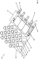
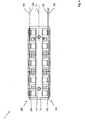
- a converter arrangement 1 comprises a first converter 100 having a first, in a first plane 102 (FIG. Fig. 5 ) arranged board 104 which carries at least a first electric power semiconductor switch 106 and at least two first power capacitors 108, 110. Furthermore, the converter arrangement 1 comprises a second converter 200, which is configured essentially identical to the first converter 100 and has a second circuit board 204 which carries at least one second power semiconductor switch 206 and at least two second power capacitors 208, 210. Apertures 112, 212 are formed in the first and second boards 104, 204, which have a diameter that is preferably slightly larger than the diameter of the head portions of the power capacitors 108, 110.
- the second circuit board 204 is arranged opposite the power capacitors 108, 110 of the first circuit board 100 in a second plane 202 extending parallel to the first plane 102.
- the spatial arrangement is such that the heads or head portions of the power capacitors 108, 110 of one board 104 extend through the openings in the other board 204, respectively.
- the boards 204, 104 are preferably connected by means of electrical terminal lugs 226, 228, 116, 118, which are led out together on one side of the board 204, 104, to an external electrical contact.
- the power semiconductor switches 206, 106 are arranged on the same side as the terminal lugs 226, 228, 116, 118 of the board next to each other and with this preferably electrically connected by means of unspecified screw, solder joints or connectors, wherein the external electrical connection of the power semiconductor switch 206, 106 preferably takes place by means of the terminal lugs.
- the electrical connection lugs 126, 128, 226, 228; 130, 230 of the respective board 104, 204 and / or a power semiconductor switch 106, 206 are preferably made of copper and plugged into a female part of an electrical connector and / or screwed with this.
- a common heat sink 10 is arranged between the electric power semiconductor switches 106, 206 of the first and second circuit boards 104, 204, which is thermally conductively coupled to the power semiconductor switches 106, 206.
- the heat sink 10 is preferably a liquid cooler whose liquid inlet 14 and liquid outlet 16 are preferably led out of the converter arrangement 1 on the same side as the electrical connection lugs 126, 128, 226, 228.
- the connecting lugs 126, 128, 226, 228 are preferably fastened in the region of the heat sink 10 with the aid of unspecified insulated spacers.
- the power capacitors 108, 110, 114, 116, 208, 210, 214, 216 are preferably cylindrical in the manner of a round cup; but can also be cuboid.
- the power capacitors are preferably arranged on a grid in such a way that the head parts of the capacitors of the one circuit board can be plugged congruently into the openings of the preferably almost identically designed second circuit board and the power capacitors 108, 110, 114, 116, 208, 210, 214 , 216 of the two boards 104, 204 interlock.
- the assembled boards 104, 204 are at least partially closed circumferentially in the region of the gap 2 by means of unspecified plates and form a mechanically stable unit in which the peripheral surfaces of the power capacitors to increase the mechanical stability to shear forces on the boards at least partially support the inner edges of the respective openings.
- each of the boards 104, 204 carries more than two, preferably more than four, more preferably up to 22 power capacitors 108, 110, 114, 116.
- the power capacitors 108, 110, 114, 116 on the respective first or second board 104, 204 are preferably arranged in parallel rows 118, 120 in a grid in such a way that between two in a row 118, 120 adjacent power capacitors 108, 110, 114, 116, a free space 122,124 is provided which is at least half the width, or half the diameter of a power capacitor 108, 110, 114, 116, but preferably the width, or the full diameter of a Power capacitor owns.
- openings 112 are preferably arranged, into which the heads of the power capacitors 208, 210, 214, 216 of the respective other board 204, 104 can be inserted.
- the power capacitors 108, 110, 114, 116, 208, 210, 214, 216 of two adjacent rows 118, 120, 218, 220 are alternately offset from one another such that the power capacitors 108, 110, 208, 210 of the one row 118, 218; 120, 220 at the level of the free spaces 124, 224; 122, 222 of the adjacent other row 120, 220; 118, 218 lie.
- Fig. 3 shown that the terminal plates 126,128,130,226,228,230 preferably outside the inverter assembly 1 along a common plane not shown in detail.
- FIGS. 4 and 5 show that the clear distance B between the first and second boards 104, 204 is less than the height A of a power capacitor 108, 110, 114, 116, 208, 210, 214, 216. Furthermore, it is shown that the electrical connections 126, 128, 226, 228; 130, 230 are led out on one side of the board 104, 206 and, viewed from the side, lie in a third and fourth plane 132, 232 extending parallel to the first and second planes 102, 202.
- the heat sink 10 comprises a liquid cooler which has at least one liquid inlet 14 and one liquid outlet 16, which are arranged in a further fifth plane 12 extending parallel to the first and second planes 102, 202.
- the liquid inlet 14 and liquid outlet 16 are preferably on the same side as the electrical connections 126, 128, 226, 228; 130, 230 led out of the region of the first and second boards 104, 204 and each preferably designed such that they can be inserted into a quick coupling.
- the electric power semiconductor switches 106, 206 are preferably insulated gate bipolar transistors (IGBTs). As in Fig. 4 2, the IGBTs 106, 206 of two nested boards 104, 204 are preferably received opposite the heat sink 10 and are connected in a heat-conducting manner to the latter.
- IGBTs 106, 206 of two nested boards 104, 204 are preferably received opposite the heat sink 10 and are connected in a heat-conducting manner to the latter.
Landscapes
- Engineering & Computer Science (AREA)
- Microelectronics & Electronic Packaging (AREA)
- Physics & Mathematics (AREA)
- Thermal Sciences (AREA)
- Inverter Devices (AREA)
Description
Die Erfindung betriff eine Umrichteranordnung gemäß dem Oberbegriff von Anspruch 1.The invention relates to a converter arrangement according to the preamble of
Umrichter und Umrichteranordnungen, insbesondere Wechselrichter oder Gleichrichter, die eine Vielzahl von Leistungshalbleiterschaltem, wie insbesondere IGBTs, sowie eine Vielzahl von Leistungskondensatoren umfassen, werden seit langem von der Anmelderin in kompakter Modulbauweise unter dem Markennamen VARIS® hergestellt und vertrieben. Die Größe der Umrichteranordnungen ist dabei maßgeblich von der Anzahl der Leistungshalbleiterschalter und der benötigten elektrischen Kapazität der Kondensatoren abhängig. Die elektrische Kapazität wird bevorzugt durch Leistungskondensatoren in der sogenannten zylindrischen Rundbecherform oder alternativ in Quaderform bereitgestellt. Aufgrund ihrer Größe und ihres Gewichts sind diese Komponenten häufig in einem Gehäuse aufgenommen, in welchem weitere zur Steuerung der Leistungshalbleiterschalter benötigte elektronische Komponenten, die sogenannten Leistungshalbleiterschalter-Treiber, aufgenommen sind. Dabei werden die Leistungshalbleiterschalter, die jeweils zugeordneten Leistungshalbleiterschalter-Treiber und die jeweils zugehörigen elektrischen Anschlüsse aus Gründen der Skalierbarkeit symmetrisch nebeneinander angeordnet.Inverter and converter arrangements, particularly inverters or rectifiers comprising a plurality of power semiconductor switches, such as IGBTs in particular, as well as a variety of power capacitors, have long been manufactured and sold by the Applicant in a compact modular design under the trade name VARIS®. The size of the converter arrangements is significantly dependent on the number of power semiconductor switches and the required electrical capacitance of the capacitors. The electrical capacitance is preferably provided by power capacitors in the so-called cylindrical round cup shape or alternatively in cuboid shape. Due to their size and weight, these components are often accommodated in a housing in which further electronic components required for controlling the power semiconductor switches, the so-called power semiconductor switch drivers, are accommodated. In this case, the power semiconductor switches, the respectively associated power semiconductor switch driver and the respectively associated electrical connections for reasons of scalability are arranged symmetrically side by side.
Die
Bei der zuvor genannten Umrichteranordnung ergibt sich das Problem, dass der benötigte Bauraum nahezu linear von der Anzahl der Leistungshalbleiterschalter einer Umrichteranordnung abhängt. Anders ausgedrückt führt eine Verdoppelung der Leistungshalbleiterschalter zu einer nahezu doppelt so großen Umrichteranordnung.In the aforementioned converter arrangement there is the problem that the required installation space depends almost linearly on the number of power semiconductor switches of an inverter arrangement. In other words, a doubling of the power semiconductor switches leads to an almost twice as large converter arrangement.
Demgemäß ist es eine Aufgabe der vorliegenden Erfindung, eine Umrichteranordnung zu schaffen, welche einen verringerten Bauraum aufweist.Accordingly, it is an object of the present invention to provide an inverter assembly having a reduced installation space.
Diese Aufgabe wird erfindungsgemäß durch die Merkmale von Anspruch 1 gelöst.This object is achieved by the features of
Weitere Merkmale der Erfindung sind in den Unteransprüchen beschrieben.Further features of the invention are described in the subclaims.
Gemäß der Erfindung umfasst eine erfindungsgemäße Umrichteranordnung einen ersten Umrichter mit einer ersten, in einer ersten Ebene angeordneten Platine, die wenigstens einen ersten elektrischen Leistungshalbleiterschalter sowie wenigstens zwei erste Leistungskondensatoren trägt. Weiterhin umfasst die Umrichteranordnung einen im Wesentlichen baugleich zum ersten Umrichter ausgebildeten zweiten Umrichter, der eine zweite Platine enthält, die wenigstens einen zweiten Leistungshalbleiterschalter und wenigstens zwei zweite Leistungskondensatoren trägt. Die Erfindung zeichnet sich dadurch aus, dass die zweite Platine den Leistungskondensatoren der ersten Platine in der Weise gegenüberliegend in einer parallel zur ersten Ebene verlaufenden zweiten Ebene angeordnet ist, dass sich die Leistungskondensatoren jeweils durch in der ersten und zweiten Platine geformte Öffnungen der jeweils gegenüberliegenden Platine hindurch, bzw. in diese hinein erstrecken.According to the invention, a converter arrangement according to the invention comprises a first converter having a first circuit board arranged in a first plane and carrying at least one first electrical power semiconductor switch and at least two first power capacitors. Furthermore, the converter arrangement comprises a second converter which is constructed essentially identical to the first converter and which contains a second circuit board which carries at least one second power semiconductor switch and at least two second power capacitors. The invention is characterized in that the second circuit board is arranged opposite to the power capacitors of the first circuit board in a second plane extending parallel to the first plane such that the power capacitors are each formed by openings of the respectively opposite circuit board formed in the first and second circuit boards through, or extend into this.
Die Erfindung besitzt den Vorteil, dass die Bauhöhe zwischen den Platinen auf weniger als die Bauhöhe der Kondensatoren verringert werden kann, wodurch die erfindungsgemäße Umrichteranordnung wesentlich kompakter ist, als zwei getrennte Umrichter, die jeweils eine eigene einzelne Platine aufweisen, auf der die Leistungshalbleiter und Kondensatoren aufgebracht sind. Aufgrund dieser besonders kompakten erfindungsgemäßen Anordnung führt eine Verdopplung von drei Leistungshalbleiterschaltern auf sechs Leistungshalbleiterschalter in einer erfindungsgemäßen Umrichteranordnung nur zu einem geringfügig vergrößerten Bauraum, da die Höhe der Umrichteranordnung maßgeblich durch die Höhe der Leistungskondensatoren bestimmt wird. Ein weiterer Vorteil der Erfindung besteht darin, dass beim Ausfall eines einzelnen Kondensators diesen nach Lösen seiner Lötverbindungen durch die zugehörige Öffnung hindurch aus dem Gesamtpaket entnommen und ausgetauscht werden kann, ohne die Anordnung insgesamt zu zerlegen.The invention has the advantage that the height between the boards can be reduced to less than the height of the capacitors, whereby the converter arrangement according to the invention is much more compact than two separate inverters, each having its own individual board on which the power semiconductors and capacitors are applied. Due to this particularly compact arrangement according to the invention, a doubling of three power semiconductor switches to six power semiconductor switches in a converter arrangement according to the invention only leads to a slightly larger installation space, since the height of the converter arrangement is significantly determined by the height of the power capacitors. Another advantage of the invention is that when a single capacitor fails, it can be removed from the overall package and replaced after loosening its solder joints through the associated aperture without disassembling the assembly as a whole.
Bei der bevorzugten Ausführungsform der Erfindung ist zwischen den elektrischen Leistungshalbleiterschaltern der ersten und zweiten Platine ein gemeinsamer Kühlkörper angeordnet, der mit den Leistungshalbleiterschaltern der ersten und zweiten Platine wärmeleitend gekoppelt ist.In the preferred embodiment of the invention, a common heat sink is disposed between the electric power semiconductor switches of the first and second circuit boards, which is thermally conductively coupled to the power semiconductor switches of the first and second circuit boards.
Diese Ausführungsform der Erfindung besitzt den Vorteil, dass lediglich ein gemeinsamer Kühlkörper für die Leistungshalbleiterschalter der ersten und zweiten Platine benötigt wird.This embodiment of the invention has the advantage that only one common heat sink is required for the power semiconductor switches of the first and second circuit boards.
Bei der bevorzugten Ausführungsform der erfindungsgemäßen Umrichteranordnung besitzen die Leistungskondensatoren eine vorzugsweise zylindrische oder quaderförmige Form.In the preferred embodiment of the converter arrangement according to the invention, the power capacitors have a preferably cylindrical or cuboid shape.
Diese Ausführungsform der erfindungsgemäßen Umrichteranordnung besitzt den Vorteil, dass die Leistungskondensatoren besonders dicht angeordnet werden können und die Öffnungen in der jeweiligen Platine besonders einfach zu fertigen sind.This embodiment of the converter arrangement according to the invention has the advantage that the power capacitors can be arranged particularly dense and the openings in the respective board are particularly easy to manufacture.
Nach einem weiteren der Erfindung zugrunde liegenden Gedanken bilden der erste und zweite Umrichter eine Einheit. Der sich ergebene Raum zwischen der ersten und zweiten Platine ist dabei vorzugsweise zumindest teilweise umfänglich geschlossen, beispielsweise durch umfänglich angeordnete Blechwände oder Kunststoffwände. Hierdurch ergibt sich eine besonders stabile und kompakte Anordnung, die zugleich auch die gezielte Durchführung von Kühlluft ermöglicht.According to another idea underlying the invention, the first and second converters form a unit. The resulting space between the first and second circuit board is preferably closed at least partially circumferentially, for example by circumferentially arranged sheet metal walls or plastic walls. This results in a particularly stable and compact arrangement, which also allows the targeted implementation of cooling air at the same time.
Bei einer weiteren Ausführungsform trägt jede der Platinen mehr als zwei, vorzugsweise vier oder mehr Leistungskondensatoren. Die Leistungskondensatoren auf der jeweiligen ersten oder zweiten Platine sind hierbei vorzugsweise in parallel verlaufenden Reihen in einem Raster in der Weise angeordnet, dass zwischen zwei in einer Reihe benachbarten Leistungskondensatoren ein Freiraum vorgesehen ist, der vorzugsweise die Breite eines Leistungskondensators, besonders bevorzugt jedoch nur etwas mehr als die halbe Breite eines Leistungskondensators besitzt. Hierdurch ergibt sich der Vorteil, dass zwischen den Kondensatorreihen gezielt Kühlluft hindurchgeblasen werden kann, die die Gehäuse der Kondensatoren zur Abfuhr von während des Betriebs entstehender Wärme wirksam umströmt.In another embodiment, each of the boards carries more than two, preferably four or more power capacitors. The power capacitors on the respective first or second board are in this case preferably arranged in parallel rows in a grid in such a way that between two adjacent in a row power capacitors, a free space is provided, preferably the width of a power capacitor, but more preferably only slightly more than half the width of a power capacitor. This results in the advantage that cooling air can be selectively blown between the rows of capacitors, which effectively flows around the housings of the capacitors for dissipating heat arising during operation.
Nach einem weiteren Gedanken der Erfindung sind die Leistungskondensatoren zweier benachbarter Reihen bei der vorherigen- Ausführungsform in vorteilhafter Weise wechselweise versetzt zueinander angeordnet, derart, dass die Leistungskondensatoren der einen Reihe in Höhe der Freiräume der benachbarten anderen Reihe angeordnet sind. Dadurch ergibt sich der Vorteil, dass die Leistungskondensatoren in einer flächenmäßig besonders dichten Packung zueinander angeordnet werden können, wobei die Reihen bei Bedarf mitunter so dicht beabstandet zueinander angeordnet werden können, dass der Abstand der Zentren der Leistungskondensatoren zweier benachbarter Reihen sogar kleiner als der Durchmesser eines Leistungskondensators gewählt werden kann.According to a further aspect of the invention, the power capacitors of two adjacent rows in the previous embodiment are advantageously arranged alternately offset from one another, such that the power capacitors of one row are arranged at the level of the free spaces of the adjacent other row. This results in the advantage that the power capacitors can be arranged in a particularly dense packing to each other in terms of area, the rows can sometimes be arranged so closely spaced from each other, if necessary, that the distance of the centers of the power capacitors of two adjacent rows even smaller than the diameter of a Power capacitor can be selected.
Bei einer weiteren Ausführungsform der Erfindung ist der lichte Abstand zwischen der ersten und zweiten Platine kleiner als die Höhe eines Leistungskondensators. Dies ergibt den Vorteil, dass die Umrichteranordnung besonders flach ausgeführt werden kann.In a further embodiment of the invention, the clear distance between the first and second circuit board is smaller than the height of a power capacitor. This results in the advantage that the converter arrangement can be made particularly flat.
Gemäß einer weiteren Ausführungsform der Erfindung weisen die Platine und/oder die Leistungshalbleiterschalter elektrische Anschlüsse auf, welche auf einer Seite der Platine herausgeführt sind und von der Seite aus betrachtet in einer parallel zur ersten und zweiten Ebene verlaufenden dritten und vierten Ebene angeordnet sind. Dies ist besonders vorteilhaft, da der elektrische Anschluss einer solchen Ausführungsform der erfindungsgemäßen Umrichteranordnung zentral von einer Seite der Anordnung aus vorgenommen werden kann.According to a further embodiment of the invention, the circuit board and / or the power semiconductor switch electrical connections, which are led out on one side of the board and viewed from the side in a parallel to the first and second plane extending third and fourth plane are arranged. This is particularly advantageous since the electrical connection of such an embodiment of the converter arrangement according to the invention can be made centrally from one side of the arrangement.
Nach einem weiteren Gedanken der Erfindung erfolgt der elektrische Anschluss der jeweiligen Platine und/oder eines Leistungshalbleiterschalters mittels einer Anschlusslasche, die vorzugsweise aus Kupfer besteht und die in eine weibliche Aufnahme, z.B. eine Buchse einer elektrischen Steckverbindung einsteckbar und/oder einschraubbar ist. Dies ermöglicht es, dass die Umrichteranordnung als eine Art steckbares Modul ausgeführt werden kann, welches beispielsweise mittels geeigneter mechanischer Führungen in eine entsprechende mechanische Aufnahme in einem Schaltschrank einschiebbar ist und anschließend mit Hilfe der Anschlüsse insbesondere durch Verschrauben elektrisch angeschlossen werden kann. Hierdurch ergibt sich der Vorteil, dass auch bei sehr hohen Strömen stets ein zuverlässiger elektrischer Kontakt erhalten wird, und dass zudem eine stabile formschlüssige mechanische Verbindung zwischen dem Schaltschrank und der erfindungsgemäßen Umricheranordnung erzeugt werden kann.According to a further aspect of the invention, the electrical connection of the respective circuit board and / or a power semiconductor switch takes place by means of a connecting lug, which preferably consists of copper and which can be inserted and / or screwed into a female receptacle, for example a socket of an electrical plug connection. This makes it possible for the converter arrangement to be designed as a type of pluggable module which can be inserted, for example by means of suitable mechanical guides, into a corresponding mechanical receptacle in a control cabinet and can then be electrically connected by means of the connections, in particular by screwing. This results in the advantage that even at very high currents always a reliable electrical contact is obtained, and that also a stable positive mechanical connection between the cabinet and the Umricheranordnung invention can be generated.
Gemäß einer weiteren Ausführungsform der Erfindung umfasst der Kühlkörper einen Flüssigkeitskühler, welcher zumindest einen Flüssigkeitseingang und Flüssigkeitsausgang aufweist, die in vorteilhafter Weise in einer weiteren parallel zur ersten und zweiten Ebene verlaufenden fünften Ebene angeordnet sind. Der Flüssigkeitseingang und Flüssigkeitsausgang sind vorzugsweise auf der gleichen Seite wie die elektrischen Anschlüsse aus dem Bereich der ersten und zweiten Platinen herausgeführt und vorzugsweise jeweils in eine Schnellkupplung einsteckbar.According to a further embodiment of the invention, the heat sink comprises a liquid cooler, which has at least one liquid inlet and liquid outlet, which are advantageously arranged in a further fifth plane extending parallel to the first and second planes. The liquid inlet and liquid outlet are preferably led out on the same side as the electrical connections from the region of the first and second boards and preferably each plugged into a quick coupling.
Nach einem weiteren der Erfindung zugrunde liegenden Gedanken ist ein elektrischer Leistungshalbleiterschalter ein Bipolartransistor mit isolierter Gate-Elektrode (IGBT). Dies hat den besonderen Vorteil, dass die erfindungsgemäße Umrichteranordnung trotz ihrer kompakten Bauweise besonders große Ströme und/oder Spannungen schalten kann. So ist die maximale Schaltspannung der Umrichteranordnung vorzugsweise größer als 100 V, bevorzugt größer als 230 V, besonders bevorzugt größer gleich 400 V; und der maximale Strom der Umrichteranordnung ist größer als 100 A, bevorzugt größer als 250 A, besonders bevorzugt größer gleich 292 A.According to another idea underlying the invention, an electric power semiconductor switch is an insulated gate bipolar transistor (IGBT). This has the particular advantage that the converter arrangement according to the invention, despite its compact design, can switch particularly large currents and / or voltages. Thus, the maximum switching voltage of the converter arrangement is preferably greater than 100 V, preferably greater than 230 V, particularly preferably greater than or equal to 400 V; and the maximum current of the converter arrangement is greater than 100 A, preferably greater than 250 A, particularly preferably greater than or equal to 292 A.
Die Erfindung wird nachfolgend mit Bezug auf die Zeichnungen anhand einer bevorzugten Ausführungsform beschrieben.The invention will be described below with reference to the drawings with reference to a preferred embodiment.
In den Zeichnungen zeigen:
- Fig. 1
- eine perspektivische Darstellung der erfindungsgemäßen Umrichteranordnung, umfassend zwei Platinen, 22 Leistungskondensatoren je Platine, drei Leistungshalbleiterschalter je Platine, zwei Anschlusslaschen je Platine und jeweils eine Anschlusslasche an einem Leistungshalbleiterschalter, sowie einen gemeinsamen Kühlkörper mit einem Flüssigkeitseingang und einem Flüssigkeitsausgang,
- Fig. 2
- eine perspektivische Darstellung eines erfindungsgemäßen Umrichters mit einem Kühlkörper,
- Fig. 3
- eine Ansicht der Unterseite einer erfindungsgemäßen Umrichteranordnung,
- Fig. 4
- eine Frontansicht der Anschlussseite einer erfindungsgemäßen Umrichteranordnung, und
- Fig. 5
- eine Seitenansicht einer erfindungsgemäßen Umrichteranordnung.
- Fig. 1
- a perspective view of the inverter assembly according to the invention, comprising two boards, 22 power capacitors per board, three power semiconductor switches per board, two terminal latches per board and one terminal lug on a power semiconductor switch, and a common heat sink with a liquid inlet and a liquid outlet,
- Fig. 2
- a perspective view of an inverter according to the invention with a heat sink,
- Fig. 3
- a view of the underside of a converter arrangement according to the invention,
- Fig. 4
- a front view of the connection side of a converter arrangement according to the invention, and
- Fig. 5
- a side view of an inverter arrangement according to the invention.
Wie in
Die Platinen 204, 104 werden vorzugsweise mittels elektrischer Anschlusslaschen 226, 228, 116, 118, welche gemeinsam an einer Seite der Platine 204, 104 herausgeführt sind, an einen extern elektrischen Kontakt angeschlossen. Wie den Figuren weiterhin zu entnehmen ist, sind die Leistungshalbleiterschalter 206, 106 auf der gleichen Seite wie die Anschlusslaschen 226, 228, 116, 118 der Platine nebeneinander angeordnet und mit dieser vorzugsweise mit Hilfe von nicht näher bezeichneten Schraubverbindungen, Lötverbindungen oder Steckverbindungen elektrisch verbunden, wobei der externe elektrische Anschluss der Leistungshalbleiterschalter 206, 106 bevorzugt mittels der Anschlusslaschen erfolgt. Dabei sind die elektrischen Anschlusslaschen 126, 128, 226, 228; 130, 230 der jeweiligen Platine 104, 204 und/oder eines Leistungshalbleiterschalters 106, 206 vorzugsweise aus Kupfer gefertigt und in einen weiblichen Teil einer elektrischen Steckverbindung einsteckbar und/oder mit diesem verschraubbar.The
Weiterhin ist zwischen den elektrischen Leistungshalbleiterschaltern 106, 206 der ersten und zweiten Platine 104, 204 ein gemeinsamer Kühlkörper 10 angeordnet, der mit den Leistungshalbleiterschaltern 106, 206 wärmeleitend gekoppelt ist. Der Kühlkörper 10 ist vorzugsweise ein Flüssigkeitskühler, dessen Flüssigkeitseingang 14 und Flüssigkeitsausgang 16 bevorzugt an derselben Seite wie die elektrischen Anschlusslaschen 126, 128, 226, 228 aus der Umrichteranordnung 1 herausgeführt sind. Die Anschlusslaschen 126,128, 226, 228 sind im Bereich des Kühlkörpers 10 bevorzugt mit Hilfe nicht näher bezeichneter isolierter Abstandshalter befestigt.Furthermore, a
Die Leistungskondensatoren 108, 110, 114, 116, 208, 210, 214, 216 sind bevorzugt zylindrisch nach Art eines Rundbechers ausgeführt; können aber auch quaderartig sein. Die Leistungskondensatoren werden bevorzugt in der Weise auf einem Raster angeordnet, dass die Kopfteile der Kondensatoren der einen Platine deckungsgleich in die Öffnungen der vorzugsweise nahezu identisch ausgeführten zweiten Platine eingesteckt werden können und die Leistungskondensatoren 108, 110, 114, 116, 208, 210, 214, 216 der beiden Platinen 104, 204 ineinander greifen. Die zusammengesteckten Platinen 104, 204 sind zumindest teilweise umfänglich im Bereich des Zwischenraums 2 mit Hilfe von nicht näher bezeichneten Platten verschlossen und bilden eine mechanisch stabile Einheit, in der sich die Umfangsflächen der Leistungskondensatoren zur Erhöhung der mechanischen Stabilität gegenüber Schubkräften auf die Platinen zumindest teilweise an den Innenrändern der jeweiligen Öffnungen abstützen.The
Wie weiterhin den
Die Leistungskondensatoren 108, 110, 114, 116, 208, 210, 214, 216 zweier benachbarter Reihen 118, 120, 218, 220 sind dabei wechselweise so versetzt zueinander angeordnet, dass die Leistungskondensatoren 108, 110, 208, 210 der einen Reihe 118, 218; 120, 220 in Höhe der Freiräume 124, 224; 122, 222 der benachbarten anderen Reihe 120, 220; 118, 218 liegen.The
Weiterhin ist in
Die
Wie den
Die elektrischen Leistungshalbleiterschalter 106, 206 sind vorzugsweise Bipolartransistoren mit isolierter Gate-Elektrode (IGBTs). Wie in
- 11
- Erfindungsgemäße UmrichteranordnungInventive inverter arrangement
- 22
- Zwischenraumgap
- 1010
- Kühlkörperheatsink
- 1212
- fünfte Ebenefifth level
- 1414
- Flüssigkeitseingangliquid inlet
- 1616
- Flüssigkeitsausgangliquid output
- 100100
- erster Umrichterfirst inverter
- 102102
- erste Ebenefirst floor
- 104104
- erste Platinefirst board
- 106106
- erster Leistungshalbleiterschalterfirst power semiconductor switch
- 108108
- Leistungskondensatorpower capacitor
- 110110
- Leistungskondensatorpower capacitor
- 112112
- Öffnungopening
- 114114
- Leistungskondensatorpower capacitor
- 116116
- Leistungskondensatorpower capacitor
- 118118
- erste Reihefirst row
- 120120
- zweite Reihesecond row
- 122122
- Freiraumfree space
- 124124
- Freiraumfree space
- 126126
- elektrischer Anschluss der Platineelectrical connection of the board
- 128128
- elektrischer Anschluss der Platineelectrical connection of the board
- 130130
- elektrischer Anschluss des Leistungshalbleiterschalterselectrical connection of the power semiconductor switch
- 132132
- dritte EbeneThird level
- 200200
- zweiter Umrichtersecond inverter
- 202202
- zweite Ebenesecond level
- 204204
- zweite Platinesecond board
- 206206
- erster Leistungshalbleiterschalterfirst power semiconductor switch
- 208208
- Leistungskondensatorpower capacitor
- 210210
- Leistungskondensatorpower capacitor
- 212212
- Öffnungopening
- 214214
- Leistungskondensatorpower capacitor
- 216216
- Leistungskondensatorpower capacitor
- 218218
- erste Reihefirst row
- 220220
- zweite Reihesecond row
- 222222
- Freiraumfree space
- 224224
- Freiraumfree space
- 226226
- elektrischer Anschluss der Platineelectrical connection of the board
- 228228
- elektrischer Anschluss der Platineelectrical connection of the board
- 230230
- elektrischer Anschluss des Leistungshalbleiterschalterselectrical connection of the power semiconductor switch
- 232232
- vierte Ebenefourth level
- AA
- Höhe eines LeistungskondensatorsHeight of a power capacitor
- BB
- lichter Abstandclear distance
Claims (11)
- A converter arrangement (1) containing a first converter (100) having a first circuit board (104), arranged in a first plane (102), which bears at least one first electrical power semiconductor switch (106) and also at least two first power capacitors (108, 110), and also having a second converter (200) of substantially identical construction to the first converter (100), which second converter comprises a second printed circuit board (204) which bears at least one second power semiconductor switch (206) and also at least two second power capacitors (208, 210),
characterised in that
the second circuit board (204) is arranged, lying opposite the power capacitors (108, 110) of the first circuit board (104), in a second plane (202) running parallel to the first plane (102), and in that openings (112, 212) are formed in the first and second circuit board (104, 204) through which the power capacitors (108, 110, 208, 210) of the circuit board (104, 204) which lies opposite in each case can be inserted. - A converter arrangement according to Claim 1,
characterised in that
a common heat sink (10) is arranged between the electrical power semiconductor switches (106, 206) of the first and second circuit boards (104, 204), which heat sink is coupled in a thermally conductive manner with the power semiconductor switches (106, 206) of the first and second circuit boards (104, 204). - A converter arrangement according to one of the preceding claims,
characterised in that
the power capacitors (108, 110, 208, 210) are of cylindrical design. - A converter arrangement according to one of the preceding claims,
characterised in that
the first and second converters (100, 200) form a unit, and the resultant gap (2) between the first and second circuit boards (104, 204) is at least partially peripherally closed. - A converter arrangement according to one of the preceding claims,
characterised in that
each of the circuit boards (104, 204) bears more than two, preferably four or more, power capacitors (108, 110, 114, 116, 208, 210, 214, 216), and in that the power capacitors (108, 110, 114, 116, 208, 210, 214, 216) are arranged on the respective first or second circuit board (104, 204) preferably in parallel rows (118, 120, 218, 220) in a grid pattern in such a manner that a clearance (122, 124, 222, 224) is provided between two adjacent power capacitors (108, 110, 114, 116) of a row (118, 120, 218, 220), which clearance is preferably at least the width of a power capacitor (108, 110, 114, 116, 208, 210, 214, 216). - A converter arrangement according to Claim 5,
characterised in that
the power capacitors (108, 110, 114, 116, 208, 210, 214, 216) of two adjacent rows (118, 120, 218, 220) are arranged alternately offset relative to each other such that the power capacitors (108, 110, 208, 210) of the first row (118, 218; 120, 220) are arranged at the level of the clearances (124, 224; 122, 222) of the adjacent second row (120, 220; 118, 218). - A converter arrangement according to one of the preceding claims,
characterised in that
the clear distance (B) between the first and second circuit board (104, 204) is less than the height (A) of a power capacitor (108, 110, 114, 116, 208, 210, 214, 216). - A converter arrangement according to one of the preceding claims,
characterised in that
the printed circuit board (104, 204) and/or the power semiconductor switches (106, 206) have electrical connections (126, 128, 226, 228; 130, 230) which are brought out on one side of the circuit board (104, 206) and, viewed from the side, are arranged in a third and fourth plane (132, 232) running parallel to the first and second plane (102, 202). - A converter arrangement according to Claim 8,
characterised in that
the electrical connection (126, 128, 226, 228; 130, 230) of the respective circuit board (104, 204) and/or of a power semiconductor switch (106, 206) is brought about by means of a connecting lug, which preferably consists of copper and can be inserted and/or screwed into a female part of an electrical plug-in connection. - A converter arrangement according to Claim 8 or 9,
characterised in that
the heat sink (10) comprises a fluid cooler which has at least one fluid inlet (14) and fluid outlet (16) arranged in a further fifth plane (12) running parallel to the first and second plane (102, 202), the fluid inlet (14) and fluid outlet (16) being brought out of the region of the first and second circuit boards (104, 204) preferably on the same side as the electrical connections (126, 128, 226, 228; 130, 230) and in each case preferably being able to be inserted into a quick coupling. - A converter arrangement according to one of the preceding claims,
characterised in that
at least one of the electrical power semiconductor switches (106, 206) is a bipolar transistor with an insulated gate electrode (IGBT).
Applications Claiming Priority (1)
| Application Number | Priority Date | Filing Date | Title |
|---|---|---|---|
| DE202016002776.0U DE202016002776U1 (en) | 2016-04-25 | 2016-04-25 | Converter arrangement |
Publications (2)
| Publication Number | Publication Date |
|---|---|
| EP3240380A1 EP3240380A1 (en) | 2017-11-01 |
| EP3240380B1 true EP3240380B1 (en) | 2018-03-21 |
Family
ID=57178181
Family Applications (1)
| Application Number | Title | Priority Date | Filing Date |
|---|---|---|---|
| EP16001990.7A Active EP3240380B1 (en) | 2016-04-25 | 2016-09-13 | Converter assembly |
Country Status (3)
| Country | Link |
|---|---|
| EP (1) | EP3240380B1 (en) |
| DE (1) | DE202016002776U1 (en) |
| ES (1) | ES2669508T3 (en) |
Families Citing this family (2)
| Publication number | Priority date | Publication date | Assignee | Title |
|---|---|---|---|---|
| DE102019209829A1 (en) * | 2019-07-04 | 2021-01-07 | Audi Ag | Apparatus comprising a heat sink and a motor vehicle |
| DE102020100360A1 (en) * | 2020-01-09 | 2021-07-15 | Bayerische Motoren Werke Aktiengesellschaft | Housing device for power electronics of a motor vehicle and a method for providing a housing device for power electronics of a motor vehicle |
Family Cites Families (4)
| Publication number | Priority date | Publication date | Assignee | Title |
|---|---|---|---|---|
| JP2012228018A (en) * | 2011-04-18 | 2012-11-15 | Yaskawa Electric Corp | Electric power conversion system |
| FI20116054L (en) * | 2011-10-26 | 2013-04-27 | John Deere Forestry Oy | Method for device of energy supply, and device for energy supply |
| CN107591998A (en) * | 2013-11-26 | 2018-01-16 | 台达电子企业管理(上海)有限公司 | Power supply change-over device and its Power convert board component |
| DE102014101024B3 (en) * | 2014-01-29 | 2014-12-04 | Semikron Elektronik Gmbh & Co. Kg | Power semiconductor device |
-
2016
- 2016-04-25 DE DE202016002776.0U patent/DE202016002776U1/en active Active
- 2016-09-13 EP EP16001990.7A patent/EP3240380B1/en active Active
- 2016-09-13 ES ES16001990.7T patent/ES2669508T3/en active Active
Non-Patent Citations (1)
| Title |
|---|
| None * |
Also Published As
| Publication number | Publication date |
|---|---|
| DE202016002776U1 (en) | 2017-07-26 |
| ES2669508T3 (en) | 2018-05-28 |
| EP3240380A1 (en) | 2017-11-01 |
Similar Documents
| Publication | Publication Date | Title |
|---|---|---|
| EP3028345B1 (en) | Contact element for a plug arrangement in a bus system, more particularly an externally routed bus system | |
| EP3605762B1 (en) | Arrangement comprising a busbar device and a converter housing and method for the production thereof, vehicle and power converter for a vehicle | |
| EP3906609B1 (en) | Electric machine | |
| DE102015113515A1 (en) | Planar capacitor connections | |
| EP1083599B1 (en) | Power semiconductor module | |
| EP2528091B1 (en) | High performance electronic system with subsystem and a cooling device | |
| DE102015105347A1 (en) | Arrangement with a conductive electronic component and with a DC busbar | |
| EP2302782A1 (en) | Frequency converter assembly | |
| EP3884742A1 (en) | Base module and functional module for a switch cabinet system | |
| DE202015004662U1 (en) | DC link capacitor module with low-inductance busbar connections | |
| EP2270821B1 (en) | Wind energy system with a converter and at least one high performance resistor | |
| EP3240380B1 (en) | Converter assembly | |
| WO2021164816A1 (en) | Power converter system | |
| WO2016030005A1 (en) | Modular assembly | |
| DE202020101852U1 (en) | Thermal interface for multiple discrete electronic devices | |
| DE102021203704A1 (en) | Half bridge, power module and inverter for an electric drive of an electric vehicle or a hybrid vehicle | |
| EP3392908B1 (en) | Power semiconductor assembly having a stack of connection panels with improved geometry for common electrical contacting of a plurality of identical power semiconductor switching elements | |
| DE60017529T2 (en) | Contacting structure for circuits of an electrical connection block and circuit-forming method | |
| DE102018221246A1 (en) | Semiconductor power module and method of connecting the same to other electrical components | |
| EP3108722A1 (en) | Printed circuit board comprising specific coupling regions | |
| DE102006032441A1 (en) | Device has printed circuit board, module which comprising electro-technical element and mechanically loadable electrical contact element on side, and module is electrically connected on side | |
| DE102022207360B3 (en) | High-current element for high-current printed circuit boards, high-current printed circuit board, use of at least one high-current element, inverter, electric drive, motor vehicle and method for producing and assembling a high-current element | |
| DE69904504T2 (en) | BUSSCHIENENVERBINDUNGSSTRUKTUR | |
| DE102022206596B4 (en) | Single phase module of an inverter, inverter and power electronics | |
| DE10236525A1 (en) | Two pair valve configuration for and electrical inverter has IGBT device on heat sink |
Legal Events
| Date | Code | Title | Description |
|---|---|---|---|
| PUAI | Public reference made under article 153(3) epc to a published international application that has entered the european phase |
Free format text: ORIGINAL CODE: 0009012 |
|
| STAA | Information on the status of an ep patent application or granted ep patent |
Free format text: STATUS: REQUEST FOR EXAMINATION WAS MADE |
|
| 17P | Request for examination filed |
Effective date: 20170309 |
|
| AK | Designated contracting states |
Kind code of ref document: A1 Designated state(s): AL AT BE BG CH CY CZ DE DK EE ES FI FR GB GR HR HU IE IS IT LI LT LU LV MC MK MT NL NO PL PT RO RS SE SI SK SM TR |
|
| AX | Request for extension of the european patent |
Extension state: BA ME |
|
| GRAP | Despatch of communication of intention to grant a patent |
Free format text: ORIGINAL CODE: EPIDOSNIGR1 |
|
| STAA | Information on the status of an ep patent application or granted ep patent |
Free format text: STATUS: GRANT OF PATENT IS INTENDED |
|
| INTG | Intention to grant announced |
Effective date: 20171211 |
|
| GRAS | Grant fee paid |
Free format text: ORIGINAL CODE: EPIDOSNIGR3 |
|
| GRAA | (expected) grant |
Free format text: ORIGINAL CODE: 0009210 |
|
| STAA | Information on the status of an ep patent application or granted ep patent |
Free format text: STATUS: THE PATENT HAS BEEN GRANTED |
|
| AK | Designated contracting states |
Kind code of ref document: B1 Designated state(s): AL AT BE BG CH CY CZ DE DK EE ES FI FR GB GR HR HU IE IS IT LI LT LU LV MC MK MT NL NO PL PT RO RS SE SI SK SM TR |
|
| RBV | Designated contracting states (corrected) |
Designated state(s): AL AT BE BG CH CY CZ DE DK EE ES FI FR GB GR HR HU IE IS IT LI LT LU LV MC MK MT NL NO PL PT RO RS SE SI SK SM TR |
|
| REG | Reference to a national code |
Ref country code: GB Ref legal event code: FG4D Free format text: NOT ENGLISH |
|
| REG | Reference to a national code |
Ref country code: CH Ref legal event code: EP |
|
| REG | Reference to a national code |
Ref country code: CH Ref legal event code: NV Representative=s name: PATENTANWALT KOELLIKER GMBH, CH |
|
| REG | Reference to a national code |
Ref country code: AT Ref legal event code: REF Ref document number: 982498 Country of ref document: AT Kind code of ref document: T Effective date: 20180415 |
|
| REG | Reference to a national code |
Ref country code: IE Ref legal event code: FG4D Free format text: LANGUAGE OF EP DOCUMENT: GERMAN |
|
| REG | Reference to a national code |
Ref country code: DE Ref legal event code: R096 Ref document number: 502016000726 Country of ref document: DE |
|
| REG | Reference to a national code |
Ref country code: DE Ref legal event code: R082 Ref document number: 502016000726 Country of ref document: DE Representative=s name: REBLE & KESSELHUT PARTNERSCHAFTSGESELLSCHAFT V, DE |
|
| REG | Reference to a national code |
Ref country code: ES Ref legal event code: FG2A Ref document number: 2669508 Country of ref document: ES Kind code of ref document: T3 Effective date: 20180528 |
|
| REG | Reference to a national code |
Ref country code: NL Ref legal event code: MP Effective date: 20180321 |
|
| PG25 | Lapsed in a contracting state [announced via postgrant information from national office to epo] |
Ref country code: HR Free format text: LAPSE BECAUSE OF FAILURE TO SUBMIT A TRANSLATION OF THE DESCRIPTION OR TO PAY THE FEE WITHIN THE PRESCRIBED TIME-LIMIT Effective date: 20180321 Ref country code: LT Free format text: LAPSE BECAUSE OF FAILURE TO SUBMIT A TRANSLATION OF THE DESCRIPTION OR TO PAY THE FEE WITHIN THE PRESCRIBED TIME-LIMIT Effective date: 20180321 Ref country code: CY Free format text: LAPSE BECAUSE OF FAILURE TO SUBMIT A TRANSLATION OF THE DESCRIPTION OR TO PAY THE FEE WITHIN THE PRESCRIBED TIME-LIMIT Effective date: 20180321 Ref country code: FI Free format text: LAPSE BECAUSE OF FAILURE TO SUBMIT A TRANSLATION OF THE DESCRIPTION OR TO PAY THE FEE WITHIN THE PRESCRIBED TIME-LIMIT Effective date: 20180321 Ref country code: NO Free format text: LAPSE BECAUSE OF FAILURE TO SUBMIT A TRANSLATION OF THE DESCRIPTION OR TO PAY THE FEE WITHIN THE PRESCRIBED TIME-LIMIT Effective date: 20180621 |
|
| REG | Reference to a national code |
Ref country code: LT Ref legal event code: MG4D |
|
| PG25 | Lapsed in a contracting state [announced via postgrant information from national office to epo] |
Ref country code: GR Free format text: LAPSE BECAUSE OF FAILURE TO SUBMIT A TRANSLATION OF THE DESCRIPTION OR TO PAY THE FEE WITHIN THE PRESCRIBED TIME-LIMIT Effective date: 20180622 Ref country code: RS Free format text: LAPSE BECAUSE OF FAILURE TO SUBMIT A TRANSLATION OF THE DESCRIPTION OR TO PAY THE FEE WITHIN THE PRESCRIBED TIME-LIMIT Effective date: 20180321 Ref country code: LV Free format text: LAPSE BECAUSE OF FAILURE TO SUBMIT A TRANSLATION OF THE DESCRIPTION OR TO PAY THE FEE WITHIN THE PRESCRIBED TIME-LIMIT Effective date: 20180321 Ref country code: SE Free format text: LAPSE BECAUSE OF FAILURE TO SUBMIT A TRANSLATION OF THE DESCRIPTION OR TO PAY THE FEE WITHIN THE PRESCRIBED TIME-LIMIT Effective date: 20180321 Ref country code: BG Free format text: LAPSE BECAUSE OF FAILURE TO SUBMIT A TRANSLATION OF THE DESCRIPTION OR TO PAY THE FEE WITHIN THE PRESCRIBED TIME-LIMIT Effective date: 20180621 |
|
| REG | Reference to a national code |
Ref country code: FR Ref legal event code: PLFP Year of fee payment: 3 |
|
| PG25 | Lapsed in a contracting state [announced via postgrant information from national office to epo] |
Ref country code: MT Free format text: LAPSE BECAUSE OF FAILURE TO SUBMIT A TRANSLATION OF THE DESCRIPTION OR TO PAY THE FEE WITHIN THE PRESCRIBED TIME-LIMIT Effective date: 20180321 |
|
| PG25 | Lapsed in a contracting state [announced via postgrant information from national office to epo] |
Ref country code: IT Free format text: LAPSE BECAUSE OF FAILURE TO SUBMIT A TRANSLATION OF THE DESCRIPTION OR TO PAY THE FEE WITHIN THE PRESCRIBED TIME-LIMIT Effective date: 20180321 Ref country code: PL Free format text: LAPSE BECAUSE OF FAILURE TO SUBMIT A TRANSLATION OF THE DESCRIPTION OR TO PAY THE FEE WITHIN THE PRESCRIBED TIME-LIMIT Effective date: 20180321 Ref country code: AL Free format text: LAPSE BECAUSE OF FAILURE TO SUBMIT A TRANSLATION OF THE DESCRIPTION OR TO PAY THE FEE WITHIN THE PRESCRIBED TIME-LIMIT Effective date: 20180321 Ref country code: EE Free format text: LAPSE BECAUSE OF FAILURE TO SUBMIT A TRANSLATION OF THE DESCRIPTION OR TO PAY THE FEE WITHIN THE PRESCRIBED TIME-LIMIT Effective date: 20180321 Ref country code: NL Free format text: LAPSE BECAUSE OF FAILURE TO SUBMIT A TRANSLATION OF THE DESCRIPTION OR TO PAY THE FEE WITHIN THE PRESCRIBED TIME-LIMIT Effective date: 20180321 Ref country code: RO Free format text: LAPSE BECAUSE OF FAILURE TO SUBMIT A TRANSLATION OF THE DESCRIPTION OR TO PAY THE FEE WITHIN THE PRESCRIBED TIME-LIMIT Effective date: 20180321 |
|
| PG25 | Lapsed in a contracting state [announced via postgrant information from national office to epo] |
Ref country code: SM Free format text: LAPSE BECAUSE OF FAILURE TO SUBMIT A TRANSLATION OF THE DESCRIPTION OR TO PAY THE FEE WITHIN THE PRESCRIBED TIME-LIMIT Effective date: 20180321 Ref country code: CZ Free format text: LAPSE BECAUSE OF FAILURE TO SUBMIT A TRANSLATION OF THE DESCRIPTION OR TO PAY THE FEE WITHIN THE PRESCRIBED TIME-LIMIT Effective date: 20180321 Ref country code: SK Free format text: LAPSE BECAUSE OF FAILURE TO SUBMIT A TRANSLATION OF THE DESCRIPTION OR TO PAY THE FEE WITHIN THE PRESCRIBED TIME-LIMIT Effective date: 20180321 |
|
| PG25 | Lapsed in a contracting state [announced via postgrant information from national office to epo] |
Ref country code: PT Free format text: LAPSE BECAUSE OF FAILURE TO SUBMIT A TRANSLATION OF THE DESCRIPTION OR TO PAY THE FEE WITHIN THE PRESCRIBED TIME-LIMIT Effective date: 20180723 |
|
| REG | Reference to a national code |
Ref country code: DE Ref legal event code: R097 Ref document number: 502016000726 Country of ref document: DE |
|
| PLBE | No opposition filed within time limit |
Free format text: ORIGINAL CODE: 0009261 |
|
| STAA | Information on the status of an ep patent application or granted ep patent |
Free format text: STATUS: NO OPPOSITION FILED WITHIN TIME LIMIT |
|
| PG25 | Lapsed in a contracting state [announced via postgrant information from national office to epo] |
Ref country code: DK Free format text: LAPSE BECAUSE OF FAILURE TO SUBMIT A TRANSLATION OF THE DESCRIPTION OR TO PAY THE FEE WITHIN THE PRESCRIBED TIME-LIMIT Effective date: 20180321 |
|
| 26N | No opposition filed |
Effective date: 20190102 |
|
| PG25 | Lapsed in a contracting state [announced via postgrant information from national office to epo] |
Ref country code: MC Free format text: LAPSE BECAUSE OF FAILURE TO SUBMIT A TRANSLATION OF THE DESCRIPTION OR TO PAY THE FEE WITHIN THE PRESCRIBED TIME-LIMIT Effective date: 20180321 |
|
| REG | Reference to a national code |
Ref country code: BE Ref legal event code: MM Effective date: 20180930 |
|
| REG | Reference to a national code |
Ref country code: IE Ref legal event code: MM4A |
|
| PG25 | Lapsed in a contracting state [announced via postgrant information from national office to epo] |
Ref country code: LU Free format text: LAPSE BECAUSE OF NON-PAYMENT OF DUE FEES Effective date: 20180913 |
|
| PG25 | Lapsed in a contracting state [announced via postgrant information from national office to epo] |
Ref country code: IE Free format text: LAPSE BECAUSE OF NON-PAYMENT OF DUE FEES Effective date: 20180913 |
|
| PG25 | Lapsed in a contracting state [announced via postgrant information from national office to epo] |
Ref country code: BE Free format text: LAPSE BECAUSE OF NON-PAYMENT OF DUE FEES Effective date: 20180930 |
|
| PG25 | Lapsed in a contracting state [announced via postgrant information from national office to epo] |
Ref country code: TR Free format text: LAPSE BECAUSE OF FAILURE TO SUBMIT A TRANSLATION OF THE DESCRIPTION OR TO PAY THE FEE WITHIN THE PRESCRIBED TIME-LIMIT Effective date: 20180321 |
|
| PG25 | Lapsed in a contracting state [announced via postgrant information from national office to epo] |
Ref country code: HU Free format text: LAPSE BECAUSE OF FAILURE TO SUBMIT A TRANSLATION OF THE DESCRIPTION OR TO PAY THE FEE WITHIN THE PRESCRIBED TIME-LIMIT; INVALID AB INITIO Effective date: 20160913 Ref country code: MK Free format text: LAPSE BECAUSE OF NON-PAYMENT OF DUE FEES Effective date: 20180321 |
|
| PG25 | Lapsed in a contracting state [announced via postgrant information from national office to epo] |
Ref country code: IS Free format text: LAPSE BECAUSE OF FAILURE TO SUBMIT A TRANSLATION OF THE DESCRIPTION OR TO PAY THE FEE WITHIN THE PRESCRIBED TIME-LIMIT Effective date: 20180721 |
|
| PG25 | Lapsed in a contracting state [announced via postgrant information from national office to epo] |
Ref country code: SI Free format text: LAPSE BECAUSE OF NON-PAYMENT OF DUE FEES Effective date: 20180913 |
|
| P01 | Opt-out of the competence of the unified patent court (upc) registered |
Effective date: 20230317 |
|
| PGFP | Annual fee paid to national office [announced via postgrant information from national office to epo] |
Ref country code: GB Payment date: 20230921 Year of fee payment: 8 Ref country code: AT Payment date: 20230915 Year of fee payment: 8 |
|
| PGFP | Annual fee paid to national office [announced via postgrant information from national office to epo] |
Ref country code: FR Payment date: 20230918 Year of fee payment: 8 Ref country code: DE Payment date: 20230919 Year of fee payment: 8 |
|
| PGFP | Annual fee paid to national office [announced via postgrant information from national office to epo] |
Ref country code: ES Payment date: 20231019 Year of fee payment: 8 |
|
| PGFP | Annual fee paid to national office [announced via postgrant information from national office to epo] |
Ref country code: CH Payment date: 20231001 Year of fee payment: 8 |