EP4258366A2 - Solarzelle und herstellungsverfahren - Google Patents
Solarzelle und herstellungsverfahren Download PDFInfo
- Publication number
- EP4258366A2 EP4258366A2 EP23193516.4A EP23193516A EP4258366A2 EP 4258366 A2 EP4258366 A2 EP 4258366A2 EP 23193516 A EP23193516 A EP 23193516A EP 4258366 A2 EP4258366 A2 EP 4258366A2
- Authority
- EP
- European Patent Office
- Prior art keywords
- emitter
- substrate
- layer
- insulating
- disposed
- Prior art date
- Legal status (The legal status is an assumption and is not a legal conclusion. Google has not performed a legal analysis and makes no representation as to the accuracy of the status listed.)
- Pending
Links
Images


Classifications
-
- H—ELECTRICITY
- H10—SEMICONDUCTOR DEVICES; ELECTRIC SOLID-STATE DEVICES NOT OTHERWISE PROVIDED FOR
- H10F—INORGANIC SEMICONDUCTOR DEVICES SENSITIVE TO INFRARED RADIATION, LIGHT, ELECTROMAGNETIC RADIATION OF SHORTER WAVELENGTH OR CORPUSCULAR RADIATION
- H10F10/00—Individual photovoltaic cells, e.g. solar cells
- H10F10/10—Individual photovoltaic cells, e.g. solar cells having potential barriers
- H10F10/16—Photovoltaic cells having only PN heterojunction potential barriers
- H10F10/164—Photovoltaic cells having only PN heterojunction potential barriers comprising heterojunctions with Group IV materials, e.g. ITO/Si or GaAs/SiGe photovoltaic cells
- H10F10/165—Photovoltaic cells having only PN heterojunction potential barriers comprising heterojunctions with Group IV materials, e.g. ITO/Si or GaAs/SiGe photovoltaic cells the heterojunctions being Group IV-IV heterojunctions, e.g. Si/Ge, SiGe/Si or Si/SiC photovoltaic cells
-
- H—ELECTRICITY
- H10—SEMICONDUCTOR DEVICES; ELECTRIC SOLID-STATE DEVICES NOT OTHERWISE PROVIDED FOR
- H10F—INORGANIC SEMICONDUCTOR DEVICES SENSITIVE TO INFRARED RADIATION, LIGHT, ELECTROMAGNETIC RADIATION OF SHORTER WAVELENGTH OR CORPUSCULAR RADIATION
- H10F10/00—Individual photovoltaic cells, e.g. solar cells
- H10F10/10—Individual photovoltaic cells, e.g. solar cells having potential barriers
- H10F10/14—Photovoltaic cells having only PN homojunction potential barriers
- H10F10/142—Photovoltaic cells having only PN homojunction potential barriers comprising multiple PN homojunctions, e.g. tandem cells
-
- H—ELECTRICITY
- H10—SEMICONDUCTOR DEVICES; ELECTRIC SOLID-STATE DEVICES NOT OTHERWISE PROVIDED FOR
- H10F—INORGANIC SEMICONDUCTOR DEVICES SENSITIVE TO INFRARED RADIATION, LIGHT, ELECTROMAGNETIC RADIATION OF SHORTER WAVELENGTH OR CORPUSCULAR RADIATION
- H10F77/00—Constructional details of devices covered by this subclass
- H10F77/30—Coatings
- H10F77/306—Coatings for devices having potential barriers
- H10F77/311—Coatings for devices having potential barriers for photovoltaic cells
-
- H—ELECTRICITY
- H10—SEMICONDUCTOR DEVICES; ELECTRIC SOLID-STATE DEVICES NOT OTHERWISE PROVIDED FOR
- H10F—INORGANIC SEMICONDUCTOR DEVICES SENSITIVE TO INFRARED RADIATION, LIGHT, ELECTROMAGNETIC RADIATION OF SHORTER WAVELENGTH OR CORPUSCULAR RADIATION
- H10F10/00—Individual photovoltaic cells, e.g. solar cells
- H10F10/10—Individual photovoltaic cells, e.g. solar cells having potential barriers
- H10F10/14—Photovoltaic cells having only PN homojunction potential barriers
- H10F10/146—Back-junction photovoltaic cells, e.g. having interdigitated base-emitter regions on the back side
-
- H—ELECTRICITY
- H10—SEMICONDUCTOR DEVICES; ELECTRIC SOLID-STATE DEVICES NOT OTHERWISE PROVIDED FOR
- H10F—INORGANIC SEMICONDUCTOR DEVICES SENSITIVE TO INFRARED RADIATION, LIGHT, ELECTROMAGNETIC RADIATION OF SHORTER WAVELENGTH OR CORPUSCULAR RADIATION
- H10F71/00—Manufacture or treatment of devices covered by this subclass
- H10F71/10—Manufacture or treatment of devices covered by this subclass the devices comprising amorphous semiconductor material
- H10F71/103—Manufacture or treatment of devices covered by this subclass the devices comprising amorphous semiconductor material including only Group IV materials
-
- H—ELECTRICITY
- H10—SEMICONDUCTOR DEVICES; ELECTRIC SOLID-STATE DEVICES NOT OTHERWISE PROVIDED FOR
- H10F—INORGANIC SEMICONDUCTOR DEVICES SENSITIVE TO INFRARED RADIATION, LIGHT, ELECTROMAGNETIC RADIATION OF SHORTER WAVELENGTH OR CORPUSCULAR RADIATION
- H10F71/00—Manufacture or treatment of devices covered by this subclass
- H10F71/121—The active layers comprising only Group IV materials
-
- H—ELECTRICITY
- H10—SEMICONDUCTOR DEVICES; ELECTRIC SOLID-STATE DEVICES NOT OTHERWISE PROVIDED FOR
- H10F—INORGANIC SEMICONDUCTOR DEVICES SENSITIVE TO INFRARED RADIATION, LIGHT, ELECTROMAGNETIC RADIATION OF SHORTER WAVELENGTH OR CORPUSCULAR RADIATION
- H10F71/00—Manufacture or treatment of devices covered by this subclass
- H10F71/128—Annealing
-
- H—ELECTRICITY
- H10—SEMICONDUCTOR DEVICES; ELECTRIC SOLID-STATE DEVICES NOT OTHERWISE PROVIDED FOR
- H10F—INORGANIC SEMICONDUCTOR DEVICES SENSITIVE TO INFRARED RADIATION, LIGHT, ELECTROMAGNETIC RADIATION OF SHORTER WAVELENGTH OR CORPUSCULAR RADIATION
- H10F71/00—Manufacture or treatment of devices covered by this subclass
- H10F71/129—Passivating
-
- H—ELECTRICITY
- H10—SEMICONDUCTOR DEVICES; ELECTRIC SOLID-STATE DEVICES NOT OTHERWISE PROVIDED FOR
- H10F—INORGANIC SEMICONDUCTOR DEVICES SENSITIVE TO INFRARED RADIATION, LIGHT, ELECTROMAGNETIC RADIATION OF SHORTER WAVELENGTH OR CORPUSCULAR RADIATION
- H10F77/00—Constructional details of devices covered by this subclass
- H10F77/20—Electrodes
- H10F77/206—Electrodes for devices having potential barriers
- H10F77/211—Electrodes for devices having potential barriers for photovoltaic cells
- H10F77/219—Arrangements for electrodes of back-contact photovoltaic cells
-
- Y—GENERAL TAGGING OF NEW TECHNOLOGICAL DEVELOPMENTS; GENERAL TAGGING OF CROSS-SECTIONAL TECHNOLOGIES SPANNING OVER SEVERAL SECTIONS OF THE IPC; TECHNICAL SUBJECTS COVERED BY FORMER USPC CROSS-REFERENCE ART COLLECTIONS [XRACs] AND DIGESTS
- Y02—TECHNOLOGIES OR APPLICATIONS FOR MITIGATION OR ADAPTATION AGAINST CLIMATE CHANGE
- Y02E—REDUCTION OF GREENHOUSE GAS [GHG] EMISSIONS, RELATED TO ENERGY GENERATION, TRANSMISSION OR DISTRIBUTION
- Y02E10/00—Energy generation through renewable energy sources
- Y02E10/50—Photovoltaic [PV] energy
- Y02E10/547—Monocrystalline silicon PV cells
-
- Y—GENERAL TAGGING OF NEW TECHNOLOGICAL DEVELOPMENTS; GENERAL TAGGING OF CROSS-SECTIONAL TECHNOLOGIES SPANNING OVER SEVERAL SECTIONS OF THE IPC; TECHNICAL SUBJECTS COVERED BY FORMER USPC CROSS-REFERENCE ART COLLECTIONS [XRACs] AND DIGESTS
- Y02—TECHNOLOGIES OR APPLICATIONS FOR MITIGATION OR ADAPTATION AGAINST CLIMATE CHANGE
- Y02P—CLIMATE CHANGE MITIGATION TECHNOLOGIES IN THE PRODUCTION OR PROCESSING OF GOODS
- Y02P70/00—Climate change mitigation technologies in the production process for final industrial or consumer products
- Y02P70/50—Manufacturing or production processes characterised by the final manufactured product
Definitions
- the present application relates to the technical field of solar cells, and particularly to a solar cell and a method for preparing the same.
- Solar cells are such devices that can directly convert solar energy into electrical energy. Since solar energy is nearly infinite and clean, solar cells have great development potential and application prospects.
- a solar cell has a front side that receives sunlight and a back side opposite to the front side.
- the solar cell has a front electrode which is disposed on the front side and a back electrode which is disposed on the back side. Electrons and holes of the photogenerated carriers are respectively collected from the front side and the back side to form a current.
- the front electrode on the front side may shield part of the sunlight entering the solar cell, reducing the light absorption efficiency of the solar cell.
- the interdigitated back contact (IBC) solar cell is a highly efficient solar cell structure whose electrodes are all disposed on the back side to improve the efficiency of the solar cell.
- IBC interdigitated back contact
- a solar cell which includes a substrate, a first emitter, a second emitter, an insulating spacing structure, a first electrode, and a second electrode.
- the substrate includes a front surface and a back surface opposite to each other.
- the first emitter and the second emitter are disposed on the back surface of the substrate.
- the doping type of the first emitter is a first doping type.
- the doping type of the second emitter is a second doping type opposite to the first doping type.
- the first electrode is disposed on a side of the first emitter away from the substrate, and the first electrode is electrically connected to the first emitter.
- the second electrode is disposed on a side of the second emitter away from the substrate, and the second electrode is electrically connected to the second emitter.
- the insulating spacing structure is disposed between the first emitter and the second emitter, and the first emitter and the second emitter are spaced from each other by the insulating spacing structure.
- the insulating spacing structure is annular shaped, the first emitter is disposed in the outer area defined by the insulating spacing structure, and the second emitter is disposed in the inner area defined by the insulating spacing structure.
- the solar cell further includes a remaining doped portion, wherein a material and a doping type of the remaining doped portion are the same as those of the first emitter, and the remaining doped portion is disposed in the inner area defined by the insulating spacing structure, and is disposed between the second emitter and the insulating spacing structure.
- the insulating spacing structure includes an annular spacing groove.
- the back surface of the substrate is exposed through the spacing groove.
- a groove width of the spacing groove is in a range from 1 ⁇ m to 100 ⁇ m.
- the insulating spacing structure further includes an insulating member disposed in the spacing groove.
- the solar cell further includes a back passivation layer disposed on the side of the first emitter away from the substrate and the side of the second emitter away from the substrate.
- the back passivation layer and the insulating member are an integrated structure.
- the solar cell further includes a passivation contact structure disposed on a surface of the first emitter away from the substrate, wherein the passivation contact structure includes a tunnel oxide layer and a polysilicon layer, the tunnel oxide layer and the polysilicon layer are sequentially stacked on the first emitter, and the polysilicon layer has the first doping type.
- the passivation contact structure includes a tunnel oxide layer and a polysilicon layer, the tunnel oxide layer and the polysilicon layer are sequentially stacked on the first emitter, and the polysilicon layer has the first doping type.
- a thickness of the tunnel oxide layer is in a range from 1 nm to 2 nm; and/or a thickness of the polysilicon layer is in a range from 10 nm to 300 nm.
- the back surface of the substrate includes a first region and a second region outside the first region, the passivation contact structure is disposed in the first region and covers the first region, and the insulating spacing structure is disposed in the second region.
- the insulating spacing structure includes a plurality of insulating spacing structures
- the second emitter includes a plurality of second emitters
- the second electrode includes a connecting portion and a plurality of electrode portions, the plurality of electrode portions are respectively in contact with the plurality of second emitters, the plurality of electrode portions are respectively disposed in the inner area defined by the plurality of insulating spacing structures, the connecting portion is connected to the plurality of electrode portions, and the plurality of electrode portions and the connecting portion are all disposed in the second region.
- a method for preparing a solar cell including steps of:
- the step of forming the insulating spacing structure includes: etching the first doped layer to form an annular spacing groove penetrating through the first doped layer, wherein the insulating spacing structure includes the spacing groove.
- the method further includes cleaning and texturing the substrate by placing the substrate in a texturizing agent, thereby forming a textured structure in the front surface of the substrate.
- the method before forming the second emitter, the method further includes: forming an insulating passivation material on the back surface of the substrate, wherein the passivation material located in the spacing groove forms an insulating member, the insulating spacing structure includes the insulating member, and the passivation material located on the first doped layer forms a back passivation layer.
- the step of forming the first doped layer includes:
- the back surface of the substrate includes a first region and a second region outside the first region, and after forming the polysilicon layer, the method further includes: removing the polysilicon layer and the tunnel oxide layer in the second region.
- the embodiments of the solar cell provided in the present application includes a first emitter and a second emitter disposed on the back surface of the substrate, and further includes an insulating spacing structure.
- the first emitter and the second emitter are spaced by the insulating spacing structure.
- the solar cell can effectively separate the first emitter from the second emitter by introducing the insulating spacing structure, avoiding the recombination of carriers on the interface between the first emitter and the second emitter, thus effectively reducing the reverse leakage of the solar cell and improving the efficiency of the solar cell.
- the reference signs and their meanings are as follows: 110, substrate; 111, first region; 112, second region; 1201, first doped layer; 121, first emitter; 122, first electrode; 131, second emitter; 132, second electrode; 1321, electrode portion; 1322, connecting portion; 140, insulating spacing structure; 141, spacing groove; 142, insulating member; 150, remaining doped portion; 161, tunnel oxide layer; 162, polysilicon layer; 171, first back passivation layer; 172, second back passivation layer; 181, first front passivation layer; 182, second front passivation layer; 210, substrate; 211, first region; 212, second region; 221, first emitter; 222, first electrode; 231, second emitter; 232, second electrode; 240, insulating spacing structure.
- the spatial relation terms such as “below”, “under”, “beneath”, “above”, “on”, “over”, etc., may be used herein to describe the relationships of an element or a feature with other elements or features shown in the drawings. It should be understood that the terms of spatial relations are intended to include other different orientations in use or operation in addition to the orientation of the elements or features shown in the drawings. For example, if the drawings are placed upside down, the element or feature which was “above” or “over” other elements or features will be “below” or “under” other elements or features. Thus, the exemplary terms “below” and “beneath” may cover the meanings of “above” or “below”.
- the element or feature can also be positioned in other different ways (e.g., rotating 90 degrees or at other orientations), and the spatial relation terms used herein can be correspondingly interpreted.
- An embodiment of the present disclosure provides a solar cell, which includes a substrate, a first emitter, a second emitter, an insulating spacing structure, a first electrode, and a second electrode.
- the substrate includes a front surface and a back surface opposite to each other.
- the first emitter and the second emitter are disposed on the back surface of the substrate.
- the doping type of the first emitter is a first doping type.
- the doping type of the second emitter is a second doping type opposite to the first doping type.
- the first electrode is disposed on a side of the first emitter away from the substrate, and the first electrode is electrically connected to the first emitter.
- the second electrode is disposed on a side of the second emitter away from the substrate, and the second electrode is electrically connected to the second emitter.
- the insulating spacing structure is disposed between the first emitter and the second emitter, and the first emitter and the second emitter are spaced from each other by the insulating spacing structure.
- the embodiment of the solar cell provided in the present application includes the first emitter and the second emitter disposed on the back surface of the substrate, and further includes the insulating spacing structure.
- the first emitter and the second emitter are spaced by the insulating spacing structure.
- the solar cell can effectively separate the first emitter from the second emitter by introducing the insulating spacing structure, avoiding the recombination of carriers on the interface between the first emitter and the second emitter, thus effectively reducing the reverse leakage of the solar cell and improving the efficiency of the solar cell.
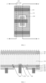
- FIG. 1 provides a schematic structural view of a back side of a solar cell.
- FIG. 2 shows an enlarged schematic view of a region A in FIG. 1 .
- FIG. 3 shows a schematic cross-sectional view along a line B-B' in FIG. 2 .
- FIG. 5 shows a schematic cross-sectional view along a line C-C' in FIG. 2 .
- a first back passivation layer 171, a second back passivation layer 172, a polysilicon layer 162, and a tunnel oxide layer 161 which are shown in FIG. 3 are omitted, so as to show a first emitter 121, a second emitter 131, and an insulating spacing structure 140.
- the solar cell includes a substrate 110, a first emitter 121, a second emitter 131, an insulating spacing structure 140, a first electrode 122, and a second electrode 132.
- the substrate 110 includes a front surface and a back surface opposite to each other.
- the upper surface of the substrate 110 is the front surface
- the lower surface is the back surface.
- the first emitter 121, the second emitter 131, the first electrode 122, and the second electrode 132 are all disposed on the back surface of the substrate 110.
- the first emitter 121 and the second emitter 131 are both disposed on the back surface of the substrate 110.
- the first emitter 121 is of a first doping type.
- the second emitter 131 is of a second doping type opposite to the first doping type.
- the first emitter 121 is configured to conduct the charge carriers corresponding to the first doping type (e.g., one of electrons or holes) to the first electrode 122
- the second emitter 131 is configured to conduct the charge carriers corresponding to the second doping type (e.g., the other of electrons or holes) to the second electrode 132.
- the first doping type can be one of P-type or N-type
- the second doping type can be the other of P-type or N-type.
- the first doping type and the second doping type can be prepared by doping different elements.
- the first doping type is N-type
- the second doping type is P-type.
- the first emitter 121 can be an N-type doped semiconductor
- the second emitter 131 can be a P-type doped semiconductor.
- the doping element for N-type doping can be a Group V element, such as phosphorus.
- the P-type doping element can be a Group III element, such as one or more of boron, aluminum, or gallium.
- the conducting type of the substrate 110 can be the same as that of the second emitter 131, and that is, the doping type of the substrate 110 is the second doping type. Further, the doping concentration of the second emitter 131 can be higher than that of the substrate 110.
- the first electrode 122 is disposed on the side of the first emitter 121 away from the substrate 110, and is electrically connected to the first emitter 121.
- the second electrode 132 is disposed on the side of the second emitter 131 away from the substrate 110, and is electrically connected to the second emitter 131. It can be understood that the first electrode 122 is electrically connected to the first emitter 121 in a manner that the first electrode 122 is in direct contact with the first emitter 121, or that another intermediate layer through which charge carriers can pass is provided between the first electrode 122 and the first emitter 121.
- the second electrode 132 is electrically connected to the second emitter 131 in a manner that the second electrode 132 is in direct contact with the second emitter 131, or that another intermediate layer through which charge carriers can pass is provided between the second electrode 132 and the second emitter 131.
- the insulating spacing structure 140 can be in an annular shape. It can be understood that the annular shape refers to a cross-section of the insulating spacing structure 140 being annular shaped, and the three-dimensional shape of the insulating spacing structure 140 can be an annular column. The annular shape can also be understood as a closed cylindrical or tubular shape. Thus, an inner area and an outer area can be defined by the insulating spacing structure 140. The outer area refers to the area outside the annular insulating spacing structure 140, and the inner area refers to the area inside and surrounded by the annular insulating spacing structure 140.
- the first emitter 121 is disposed in the outer area defined by the insulating spacing structure 140, and the second emitter 131 is disposed in the inner area defined by the insulating spacing structure 140, so that the first emitter 121 is spaced from the second emitter 131 by the insulating spacing structure 140.
- the insulating spacing structure 140 insulates and separates the inner area from the outer area.
- the insulating spacing structure 140 can be an insulating groove that separates the inner area from the outer area, or can be an insulating material that separates the inner area from the outer area, or can be an insulating groove filled with an insulating material that separates the inner area from the outer area.
- the insulating spacing structure 140 includes an annular spacing groove 141, and the spacing groove 141 is defined between the first emitter 121 and the second emitter 131, thereby electrically insulating the first emitter 121 from the second emitter 131.
- the spacing groove 141 can be formed by etching, e.g., laser etching.
- the first doped layer 1201 can be etched until the substrate 110 is exposed, thereby electrically insulating the first emitter 121 from the second emitter 131.
- the bottom wall of the spacing groove 141 is the exposed surface of the substrate 110.
- the substrate 110 is cleaned after the etching step for forming the spacing groove 141. This process also textures the surface of the substrate 110 to form a textured structure in the bottom wall of the spacing groove 141, which adversely affects the light absorption efficiency on the front side of the substrate 110.
- the groove width of the spacing groove 141 is equal to or smaller than 100 ⁇ m.
- the width of the spacing groove 141 is equal to or smaller than 100 ⁇ m, the negative effect of the textured structure of the bottom wall of the spacing groove 141 on the light absorption efficiency can be reduced as much as possible, and the requirement of processing speed in the actual preparation process can be met as well.
- the groove width of the spacing groove 141 is in a range from 1 ⁇ m to 100 ⁇ m, in order to ensure effective insulation of the spacing groove 141 while reducing the negative effect of the textured structure of the bottom wall of the spacing groove 141 on the light absorption efficiency. In some examples, the groove width of the spacing groove 141 is in a range from 10 ⁇ m to 50 ⁇ m. Further optionally, the groove width of the spacing groove 141 is in a range from 15 ⁇ m to 30 ⁇ m.
- the insulating spacing structure 140, the first emitter 121, and the second emitter 131 are disposed in the same layer.
- the spacing groove 141 further includes a cylindrical outer sidewall and a cylindrical inner sidewall both connected to the bottom wall.
- the first emitter 121 participates in forming the cylindrical outer sidewall of the spacing groove 141
- the second emitter 131 participates in forming the cylindrical inner sidewall of the spacing groove 141.
- the solar cell further includes a remaining doped portion 150.
- the material and doping type of the remaining doped portion 150 are the same as those of the first emitter 121.
- the remaining doped portion 150 is disposed in the inner area surrounded by the insulating spacing structure 140, and is disposed between the second emitter 131 and the insulating spacing structure 140.
- the solar cell further includes a passivation contact structure.
- the passivation contact structure includes a tunnel oxide layer 161 and a polysilicon layer 162.
- the tunnel oxide layer 161 and the polysilicon layer 162 are sequentially stacked on the surface of the first emitter 121 at the side away from the substrate 110.
- the polysilicon layer 162 is of the first doping type.
- the passivation contact structure is configured to reduce carrier recombination due to the contact between the first emitter 121 and the first electrode 122, thereby improving the efficiency.
- the tunnel oxide layer 161 shall be relatively thin in thickness, so that the carriers can pass through the tunnel oxide layer 161 and be transported into the polysilicon layer 162.
- the thickness of the tunnel oxide layer 161 is in a range from 1 nm to 2 nm.
- the thickness of the polysilicon layer 162 is in a range from 10 nm to 300 nm.
- the back surface of the substrate 110 includes a first region 111 and a second region 112 outside the first region 111.
- the region indicated in the dotted line block is the second region 112
- the region indicated outside the dotted line block is the first region 111.
- the passivation contact structure is disposed in the first region 111 and covers the first region 111 of the back surface of the substrate 110
- the insulating spacing structure 140 is disposed in the second region 112 of the back surface of the substrate 110.
- the passivation contact structure on the second region 112 can be removed by etching, so that the passivation contact structure only covers the first region 111.
- the inner area surrounded by the insulating spacing structure 140 can also be located in the second region 112, while the second emitter 131 is also located in the second region 112.
- the second region 112 is a continuous region located in the first region 111.
- the second electrode 132 includes a connecting portion 1322 and a plurality of electrode portions 1321.
- the plurality of electrode portions 1321 are respectively in contact with the plurality of second emitters 131.
- the electrode portions 1321 are respectively disposed in the inner areas defined by the plurality of insulating spacing structures 140.
- the connecting portion 1322 is connected to the electrode portions 1321.
- the plurality of electrode portions 1321 and the connecting portion 1322 are all disposed in the second region 112.
- FIG. 3 shows a connecting portion 1322 of the second electrode 132, and the connecting portion 1322 is configured to electrically connect adjacent electrode portions 1321.
- the front surface of the substrate 110 has a textured structure to obtain higher light absorption efficiency, while the bottom wall of the spacing groove 141 also has a textured structure.
- the textured structures of the front surface and the back surface of the substrate 110 can be formed simultaneously in a same step, or can be formed separately in different steps.
- the insulating spacing structure 140 further includes an insulating member 142 disposed in the spacing groove 141.
- the solar cell can include an insulating first back passivation layer 171.
- the first back passivation layer 171 can be disposed on a side of the first emitter 121 away from the substrate 110 and on a side of the second emitter 131 away from the substrate 110.
- the first back passivation layer 171 can be integrated with the insulating member 142.
- the first back passivation layer 171 is configured to passivate the surface of the solar cell.
- the passivation layer is usually disposed on the surface of the emitter layer to reduce the carrier recombination at the surface.
- the first back passivation layer 171 and the insulating member 142 are integrated with each other, which not only simplifies the preparation process, but also reduces the carrier recombination at the interface between the first emitter 121 and the second emitter 131 by using the same material as that of the passivation layer to form the insulating member 142.
- the solar cell can further include a second back passivation layer 172.
- the second back passivation layer 172 is disposed on the side of the first back passivation layer 171 away from the substrate 110.
- the second back passivation layer 172 is in contact with the first back passivation layer 171.
- the second back passivation layer 172 and the first back passivation layer 171 form a passivation layer stack to further improve the passivation effect.
- the materials of the first back passivation layer 171 and the second back passivation layer 172 are each independently selected from one or more of silicon nitride, aluminum oxide, titanium oxide, silicon oxide or silicon oxynitride.
- the material of the first back passivation layer 171 can be different from that of the second back passivation layer 172.
- the solar cell can further include a first front passivation layer 181 and a second front passivation layer 182.
- the first front passivation layer 181 and the second front passivation layer 182 are sequentially stacked on the front surface of the substrate 110.
- the first front passivation layer 181 and the second front passivation layer 182 form a passivation layer stack to further improve the passivation effect.
- the materials of the first front passivation layer 181 and the second front passivation layer 182 are each independently selected from one or more of silicon nitride, aluminum oxide, titanium oxide, silicon oxide, or silicon oxynitride.
- a part of the outer edge of the insulating spacing structure 140 can be in alignment with the edge of the second region 112.
- a remaining doped portion 150 can be disposed in the inner area surrounded by the insulating spacing structure 140.
- the remaining doped portion 150 is located between the second emitter 131 and the insulating spacing structure 140.
- the material and doping type of the remaining doped portion 150 can be the same as those of the first emitter 121.
- FIG. 6 is a schematic structural view of a back side of a solar cell according to another embodiment of the present application.
- the solar cell includes a substrate 210, a first emitter 221, a second emitter 231, a first electrode 222, a second electrode 232, and an insulating spacing structure 240.
- the back surface of the substrate 210 includes a first region 211 and a second region 212.
- the relative positional relationships among the various components are similar to those of the solar cell in FIG. 1 , and are not repeated herein.
- the difference from the solar cell shown in FIG. 1 is that only the second emitter 231 is disposed in the inner area surrounded by the insulating spacing structure 240, without a remaining doped portion. In this case, the cylindrical inner sidewall of the insulating spacing structure 240 is in close contact with the edge of the second emitter 231.
- cylindrical outer sidewall of the insulating spacing structure 240 can be located between the edge of the second region 212 and the edge of the second emitter 231.
- an embodiment of the present disclosure provides a method for preparing the above-described solar cell, and the method including the following steps of:
- the annular insulating spacing structure is formed in the first doped layer, and then the second emitter is formed in the inner area surrounded by the annular insulating spacing structure, so that the first emitter and the second emitter are insulated and spaced from each other, avoiding carrier recombination at the interface between the first emitter and the second emitter to reduce leakage current.
- the first doped layer in the inner area surrounded by the insulating spacing structure can be used as a protective layer to prevent texturing the substrate in the inner area, thereby reducing the adversely effect of forming the insulating spacing structure on the light absorption efficiency of the solar cell.
- the step of forming the insulating spacing structure includes a step of etching the first doped layer to form an annular spacing groove penetrating through the first doped layer, wherein the insulating spacing structure includes the spacing groove.
- the method further includes cleaning and texturing the substrate by placing the substrate in a texturizing agent after forming the spacing groove, thereby forming a textured structure in the front surface of the substrate and the bottom wall of the spacing groove.
- the method before forming the second emitter, further includes a step of forming an insulating passivation material on the back side of the substrate, wherein the passivation material located in the spacing groove forms an insulating member, and the insulating spacing structure includes the insulating member; the passivation material located on the first doped layer forms the back passivation layer.
- the step of forming the first doped layer includes: sequentially forming a tunnel oxide layer and a silicon material layer on the back side of the substrate; diffusing a doping element into the silicon material layer; and annealing the silicon material layer to form a polysilicon layer having a first doping type.
- the doping element is diffused into the substrate material, thereby forming the first doped layer that covers the substrate.
- the back surface of the substrate includes a first region and a second region outside the first region.
- the method further includes removing the polysilicon layer and the tunnel oxide layer in the second region when the polysilicon layer is formed.
- FIG. 7 shows a flow chart of the method for preparing the solar cell in FIG. 1 .
- the embodiment of the method for preparing the solar cell includes steps S1 to S6.
- step S1 a substrate is provided.
- the substrate 110 includes a front surface and a back surface opposite to each other.
- the back surface of the substrate 110 is located at the lower side of the substrate 110.
- the material of the substrate 110 can be silicon, such as single-crystal silicon.
- the doping type of the substrate 110 can be a second doping type.
- the substrate 110 is made of P-type doped silicon.
- the method further includes a step of texturizing the front surface of the substrate 110.
- the step of texturing the front surface of the substrate 110 can include: placing the substrate 110 in a texturizing agent to form a textured structure in the front surface of the substrate 110.
- the textured structure can be pyramid-shaped.
- the method further includes a step of polishing the back surface of the substrate 110.
- a chemical polishing agent can be used for polishing.
- the back surface of the substrate 110 includes a first region 111 and a second region 112.
- the second region 112 corresponds to the part to be removed in the passivation contact structure subsequently prepared, and the first region 111 is located outside the second region 112.
- step S2 a first doped layer is formed on the substrate.
- the first doped layer 1201 can be formed using the same material as that of the substrate 110, or using a new material deposited on the surface of the substrate 110. In some examples of the present embodiment, the first doped layer 1201 can be formed by doping the back surface of the substrate 110.
- the doping type of the first doped layer 1201 is N-type, and the first doped layer 1201 can be formed by diffusing phosphorus into the back surface of the substrate 110.
- the step of forming the first doped layer 1201 can include: sequentially forming a tunnel oxide layer 161 and a silicon material layer on the back surface of the substrate 110; diffusing a doping element into the silicon material layer; and annealing the silicon material layer to form a polysilicon layer 162 having a first doping type. It can be understood that during the doping element diffusion and annealing, the doping element also diffuses into the material of the substrate 110 to form the first emitter 121 covering the substrate 110. In this way, not only the first emitter 121 with the first doping type but also a passivation contact structure is formed on the substrate 110, reducing the interface recombination and further improving the efficiency of the solar cell.
- FIG. 9 shows a schematic structural view of further forming a first doped layer 1201, a tunnel oxide layer 161, and a polysilicon layer 162 on the basis of the structure shown in FIG. 8 .
- the first doped layer 1201 covers the back surface of the substrate 110.
- the first doped layer 1201 is used to form the first emitter 121 in the subsequent preparation process. It can be understood that only a part of the first doped layer 1201 is used as the first emitter 121, and the other part of the first doped layer 1201 is removed in the subsequent preparation process. Optionally, some part of the first doped layer 1201 is not removed but remains as a non-active part.
- the method when the first doped layer 1201 is formed, the method further includes a step of removing the wraparound material on the lateral surface and the front surface of the substrate 110.
- the passivation contact structure includes the stacked tunnel oxide layer 161 and polysilicon layer 162.
- the step of forming the passivation contact structure includes: sequentially forming the tunnel oxide layer 161 and the polysilicon layer 162 on the first doped layer 1201, wherein the doping type of the polysilicon layer 162 is the first doping type.
- the tunnel oxide layer 161 can be formed by partially oxidizing the first doped layer 1201, or can be formed by depositing the tunnel oxide layer 161 on the first doped layer 1201. In some examples of the present embodiment, the tunnel oxide layer 161 is formed on the first doped layer 1201 by chemical vapor deposition.
- the polysilicon layer 162 can be formed by deposition. Further, the polysilicon layer 162 can be directly doped during the deposition process, or can be doped when the polysilicon layer 162 is formed. In some examples of the present embodiment, an amorphous silicon layer is first deposited on the surface of the tunnel oxide layer 161 by chemical vapor deposition, then the amorphous silicon layer is doped, and then the amorphous silicon layer is annealed to obtain the polysilicon layer 162 with the first doping type.
- step S2 the tunnel oxide layer 161 and the polysilicon layer 162 both cover the entire first doped layer 1201.
- step S3 the polysilicon layer and the tunnel oxide layer in the second region are removed.
- FIG. 10 shows a schematic structural view of removing a part of the polysilicon layer and a part of the tunnel oxide layer on the basis of the structure shown in FIG. 9 .
- the part of the polysilicon layer 162 and the part of the tunnel oxide layer 161 located in the second region 112 are removed. It can be understood that there is no polysilicon layer 162 or tunnel oxide layer 161 in the second region 112.
- the polysilicon layer 162 and the tunnel oxide layer 161 can be removed by etching.
- the specific way of etching can be selected from wet etching or laser etching.
- the polysilicon layer 162 and the tunnel oxide layer 161 are removed by laser etching.
- the first doped layer 1201 in the second region 112 can function as a protective layer for the substrate 110.
- step S4 an annular spacing groove is formed in the first doped layer.
- the step of forming the spacing groove 141 includes a step of removing a part of the first doped layer 1201 to form the annular spacing groove 141.
- FIG. 11 shows a schematic structural view of forming a spacing groove 141 on the basis of the structure shown in FIG. 10 .
- a part of the first doped layer 1201 in the second region 112 is removed to form the annular spacing groove 141.
- the first doped layer 1201 located in the outer area outside the spacing groove 141 functions as the first emitter 121, while the first doped layer 1201 located in the inner area surrounded by the spacing groove 141 is remained and functions as a remaining doped portion 150.
- the first emitter 121 is insulated and spaced from the remaining doped portion 150.
- the spacing groove 141 penetrates through the first doped layer 1201, so that the bottom of the spacing groove 141 is the substrate 110.
- the first doped layer 1201 is removed by laser etching.
- the groove width of the spacing groove 141 is controlled to be smaller than or equal to 100 ⁇ m. Further, the groove width of the spacing groove 141 can be controlled in a range from 1 ⁇ m to 100 ⁇ m. In some examples, the groove width of the spacing groove 141 is in a range from10 ⁇ m to 50 ⁇ m. Further optionally, the groove width of the spacing groove 141 is in a range from 15 ⁇ m to 30 ⁇ m.
- the spacing groove 141 is formed by laser etching, the surface of the substrate 110 still has residual materials, so the substrate 110 needs to be chemically cleaned.
- the substrate 110 is chemically cleaned with a texturing agent, so as to form a textured structure in the front surface of the substrate 110 while cleaning the substrate 110, which simplifies the preparation process. It can be understood that the substrate 110 in the inner area surrounded by the spacing groove 141 is covered by the remaining doped portion 150, and thus only the part of the back surface of the substrate 110 exposed through the spacing groove 141 will be formed with a textured structure.
- the entire area (i.e., the second region 112) of the substrate 110 which is not covered by the remaining doped portion 150 will be formed with a textured structure, which will significantly reduce the light absorption efficiency of the substrate 110, resulting in low efficiency of the solar cell.
- step S5 a first back passivation layer, a second back passivation layer, a first front passivation layer, and a second front passivation layer are formed.
- FIG. 12 shows a schematic structural view of forming a passivation stack on the basis of the structure shown in FIG. 11 .
- the first back passivation layer 171 covers the back side of the substrate 110. Further, when forming the first back passivation layer 171, the passivation material is also filled in the spacing groove 141 to form the insulating member 142. It can be understood that the passivation material can be selected from insulating materials to prevent electrical conduction between the first emitter 121 and the remaining doped portion 150.
- the first back passivation layer 171 and the first front passivation layer 181 are made of the same material. During the preparation process, the first back passivation layer 171 and the first front passivation layer 181 can be formed on the front side and the back side of the substrate 110 at the same time.
- the second back passivation layer 172 and the second front passivation layer 182 are then formed.
- the second back passivation layer 172 and the second front passivation layer 182 are made of the same material. During the preparation process, the second back passivation layer 172 and the second front passivation layer 182 can be formed on the front side and the back side of the substrate 110 at the same time.
- step S6 a second emitter, a first electrode, and a second electrode are formed.
- the solar cell with the cross-sectional structure as shown in FIG. 3 can be formed.
- the first electrode 122 passes through the first back passivation layer 171 and the second back passivation layer 172, and comes into contact with the polysilicon layer 162.
- the first electrode 122 is electrically connected to the first emitter 121 through the tunnel oxide layer 161 and the polysilicon layer 162.
- the tunnel oxide layer 161 and the polysilicon layer 162 are etched first to form a first connection hole, and then a conductive material is filled in the first connection hole to form the first electrode 122.
- the material of the first electrode 122 can be one or more of silver or copper.
- the second emitter 131 can be formed by co-sintering the material of the second electrode 132 and the material of the substrate 110.
- the second electrode 132 passes through the first back passivation layer 171 and the second back passivation layer 172, and the second electrode 132 is in contact with the second emitter 131.
- the tunnel oxide layer 161 and the polysilicon layer 162 can be etched first to form a second connection hole, then the material of the second electrode 132 is filled in the second connection hole, and then the structure is sintered to form the second emitter 131 and the second electrode 132.
- the material of the second electrode 132 can include aluminum.
- the solar cell structure in the embodiment of the present disclosure can be prepared through steps S1 to S6.
- the present application further provides the following examples and comparative examples.
- the advantages of the solar cell according to the embodiments of the present application will be apparent through the differences between the examples and comparative examples.
- a P-type single-crystal silicon wafer is used as the substrate, which is alkali polished to remove the surface layer containing mechanical damages and the pollutants on the substrate.
- a tunnel oxide layer with a thickness of 2 nm and an amorphous silicon layer with a thickness of 100 nm are deposited on the back side of the substrate. Then the amorphous silicon layer is doped with phosphorus and annealed, so that the amorphous silicon layer is converted into an N-type polysilicon layer and a first doped layer is formed between the tunnel oxide layer and the substrate.
- the polysilicon layer and the tunnel oxide layer in the second region are removed by laser etching to expose the first doped layer.
- a plurality of annular spacing grooves are formed by laser etching the first doped layer in the second region, and the groove width of the spacing groove is 25 ⁇ m.
- the first doped layer in the outer area outside the annular spacing grooves functions as the first emitter, and the first doped layer in the inner area of the annular spacing grooves forms the remaining doped portion.
- the substrate is cleaned and textured in a texturing agent to form a textured structure in the front surface of the substrate and the back surface of the substrate exposed through the spacing grooves.
- Aluminum oxide layers are deposited on both the front and back sides of the substrate as the first front passivation layer and first back passivation layer, and then silicon nitride layers are deposited as the second front passivation layer and second back passivation layer.
- first connection holes are formed at the position corresponding to the first electrodes, exposing a part of the polysilicon layer, and second connection holes are formed at the position corresponding to the second electrodes, exposing a part of the substrate in the second region.
- a silver paste is screen-printed on the exposed polysilicon layer, and an aluminum paste is screen-printed on the exposed substrate in the second region, which are both sintered, thereby forming second emitters from the part of the aluminum paste that is in contact with the substrate, forming first electrodes from the silver paste , and forming second electrodes from the aluminum paste.
- a P-type single-crystal silicon wafer is used as the substrate, which is alkali polished to remove the surface layer containing mechanical damages and the pollutants on the substrate. Then a textured structure is formed in the front surface of the substrate.
- a tunnel oxide layer with a thickness of 2 nm and an amorphous silicon layer with a thickness of 100 nm are deposited on the back side of the substrate. Then the amorphous silicon layer is doped with phosphorus and annealed, so that the amorphous silicon layer is converted into an N-type polysilicon layer, and a first doped layer is formed between the tunnel oxide layer and the substrate.
- the polysilicon layer and the tunnel oxide layer in the second region are removed by laser etching to expose the first doped layer.
- a plurality of annular spacing grooves are formed by laser etching the first doped layer in the second region, and the groove width of the spacing groove is 20 ⁇ m.
- the first doped layer in the outer area outside the annular spacing grooves functions as the first emitter, and the first doped layer in the inner area surrounded by the annular spacing grooves forms the remaining doped portion. Then the substrate is cleaned with a texturing agent.
- Aluminum oxide layers are deposited on both the front and back sides of the substrate as the first front passivation layer and first back passivation layer, and then silicon nitride layers are deposited as the second front passivation layer and second back passivation layer.
- first connection holes are formed at the position corresponding to the first electrodes, exposing a part of the polysilicon layer, and second connection holes are formed at the position corresponding to the second electrodes, exposing a part of the substrate in the second region.
- a silver paste is screen-printed on the exposed polysilicon layer, and an aluminum paste is screen-printed on the exposed substrate in the second region, which are both sintered, thereby forming second emitters from the part of the aluminum paste that is in contact with the substrate, forming first electrodes from the silver paste, and forming second electrodes from the aluminum paste.
- a P-type single-crystal silicon wafer is used as the substrate, which is alkali polished to remove the surface layer containing mechanical damages and the pollutants on the substrate.
- the back surface of the substrate is doped with phosphorus to form an N-type first doped layer.
- a tunnel oxide layer with a thickness of 2 nm and an amorphous silicon layer with a thickness of 100 nm are deposited on the back side of the substrate. Then the amorphous silicon layer is doped with phosphorus and annealed, so that the amorphous silicon layer is converted into an N-type polysilicon layer.
- the polysilicon layer and the tunnel oxide layer in the second region are removed by wet etching.
- the substrate is cleaned and textured in a texturing agent to form a textured structure in the front surface of the substrate.
- Aluminum oxide layers are deposited on both the front and back sides of the substrate as the first front passivation layer and first back passivation layer, and then silicon nitride layers are deposited as the second front passivation layer and second back passivation layer.
- first connection holes are formed at the position corresponding to the first electrodes, exposing the polysilicon layer in the N region, and second connection holes are formed at the position corresponding to the second electrodes, exposing the substrate in the P region.
- a silver paste is screen-printed in the N region, and an aluminum paste is screen-printed in the P region, which are both sintered, thereby forming second emitters from the part of the aluminum paste that is in contact with the substrate, forming first electrodes from the silver paste, and forming second electrode from the aluminum paste .
- a P-type single-crystal silicon wafer is used as the substrate, which is alkali polished to remove the surface layer containing mechanical damages and the pollutants on the substrate.
- a tunnel oxide layer with a thickness of 2 nm and an amorphous silicon layer with a thickness of 100 nm are deposited on the back side of the substrate. Then the amorphous silicon layer is doped with phosphorus and annealed, so that the amorphous silicon layer is converted into an N-type polysilicon layer and a first doped layer is formed between the tunnel oxide layer and the substrate.
- the polysilicon layer and the tunnel oxide layer in the second region are removed by laser etching to expose the first doped layer.
- the first doped layer in the entire of the second region are removed by laser etching. Then the substrate is cleaned and textured in a texturing agent to form a textured structure in the front surface of the substrate and the second region of the back surface of the substrate.
- Aluminum oxide layers are deposited on both the front and back sides of the substrate as the first front passivation layer and first back passivation layer, and then silicon nitride film layers are deposited as the second front passivation layer and second back passivation layer;
- first connection holes are formed at the position corresponding to the first electrodes, exposing a part of the polysilicon layer, and second connection holes are formed at the position corresponding to the second electrodes, exposing a part of the substrate in the second region.
- a silver paste is screen-printed on the exposed polysilicon layer, and an aluminum paste is screen-printed on the exposed substrate in the second region, which are both sintered, thereby forming second emitters from the part of the aluminum paste that is in contact with the substrate, forming first electrodes from the silver paste, and forming second electrodes from the aluminum paste.
- the reverse leakage current of the solar cell in Comparative Example 1 is significantly larger.
- the main reason is that no spacing groove or insulating spacing structure is formed between the first emitter and the second emitter in Comparative Example 1, which results in a relatively high leakage current.
- the efficiency is also significantly reduced, which is mainly due to the completely removal of the first doped layer from the second region followed by the texturing step, so that the entire second region has a textured structure, leading to the reduced efficiency.
- the sequence of the steps is not strictly limited, and the steps may be performed in other orders. Moreover, at least some of the steps may include multiple sub-steps or multiple stages, these sub-steps or stages are not necessarily performed at the same time, but may be performed at different times. These sub-steps or stages are not necessarily to be sequentially performed, but can be performed alternately or in turn with at least some of the sub-steps or stages of other steps.
Landscapes
- Photovoltaic Devices (AREA)
- Life Sciences & Earth Sciences (AREA)
- Engineering & Computer Science (AREA)
- Sustainable Energy (AREA)
- Sustainable Development (AREA)
Applications Claiming Priority (1)
| Application Number | Priority Date | Filing Date | Title |
|---|---|---|---|
| CN202310341102.9A CN116314361B (zh) | 2023-03-31 | 2023-03-31 | 太阳电池及太阳电池的制备方法 |
Publications (2)
| Publication Number | Publication Date |
|---|---|
| EP4258366A2 true EP4258366A2 (de) | 2023-10-11 |
| EP4258366A3 EP4258366A3 (de) | 2024-03-27 |
Family
ID=86795812
Family Applications (1)
| Application Number | Title | Priority Date | Filing Date |
|---|---|---|---|
| EP23193516.4A Pending EP4258366A3 (de) | 2023-03-31 | 2023-08-25 | Solarzelle und verfahren zu ihrer herstellung |
Country Status (5)
| Country | Link |
|---|---|
| US (1) | US12433037B2 (de) |
| EP (1) | EP4258366A3 (de) |
| JP (1) | JP7583883B2 (de) |
| CN (2) | CN120547982A (de) |
| AU (1) | AU2023216789B2 (de) |
Families Citing this family (7)
| Publication number | Priority date | Publication date | Assignee | Title |
|---|---|---|---|---|
| CN117276361B (zh) * | 2023-11-22 | 2024-02-02 | 天合光能股份有限公司 | 太阳能电池及其制作方法、光伏组件及光伏系统 |
| CN118053924A (zh) | 2024-02-06 | 2024-05-17 | 浙江晶科能源有限公司 | 太阳能电池及其制备方法、叠层电池和光伏组件 |
| CN119630068A (zh) * | 2024-02-07 | 2025-03-14 | 隆基绿能科技股份有限公司 | 一种背接触电池及光伏组件 |
| CN120614904A (zh) * | 2024-03-04 | 2025-09-09 | 天合光能股份有限公司 | 背接触太阳能电池和光伏组件 |
| CN118335845A (zh) * | 2024-04-26 | 2024-07-12 | 天合光能股份有限公司 | 全背接触电池制造方法、全背接触电池及光伏组件 |
| CN118156342B (zh) * | 2024-05-10 | 2024-08-20 | 金阳(泉州)新能源科技有限公司 | 一种具有耐酸绝缘隔离区的背接触电池及其制作和应用 |
| CN118412387A (zh) * | 2024-07-03 | 2024-07-30 | 天合光能股份有限公司 | 太阳能电池、光伏组件和太阳能电池的制造方法 |
Family Cites Families (26)
| Publication number | Priority date | Publication date | Assignee | Title |
|---|---|---|---|---|
| JP2003124483A (ja) * | 2001-10-17 | 2003-04-25 | Toyota Motor Corp | 光起電力素子 |
| US20090101197A1 (en) * | 2005-05-11 | 2009-04-23 | Mitsubishi Electric Corporation | Solar Battery and Production Method Thereof |
| JP2009158575A (ja) * | 2007-12-25 | 2009-07-16 | Sharp Corp | 光電変換装置および光電変換装置の製造方法 |
| US7851698B2 (en) * | 2008-06-12 | 2010-12-14 | Sunpower Corporation | Trench process and structure for backside contact solar cells with polysilicon doped regions |
| JP2011181606A (ja) * | 2010-02-26 | 2011-09-15 | Sharp Corp | 太陽電池素子およびその製造方法 |
| US8134217B2 (en) * | 2010-12-14 | 2012-03-13 | Sunpower Corporation | Bypass diode for a solar cell |
| US8889981B2 (en) * | 2011-10-18 | 2014-11-18 | Samsung Sdi Co., Ltd. | Photoelectric device |
| CN202363468U (zh) * | 2011-12-08 | 2012-08-01 | 常州天合光能有限公司 | 点接触背发射极异质结太阳电池 |
| US9054255B2 (en) * | 2012-03-23 | 2015-06-09 | Sunpower Corporation | Solar cell having an emitter region with wide bandgap semiconductor material |
| US8785233B2 (en) * | 2012-12-19 | 2014-07-22 | Sunpower Corporation | Solar cell emitter region fabrication using silicon nano-particles |
| US9312406B2 (en) * | 2012-12-19 | 2016-04-12 | Sunpower Corporation | Hybrid emitter all back contact solar cell |
| KR101613843B1 (ko) * | 2013-04-23 | 2016-04-20 | 엘지전자 주식회사 | 태양 전지 및 이의 제조 방법 |
| KR101622089B1 (ko) * | 2013-07-05 | 2016-05-18 | 엘지전자 주식회사 | 태양 전지 및 이의 제조 방법 |
| CN103794679B (zh) * | 2014-01-26 | 2016-07-06 | 晶澳(扬州)太阳能科技有限公司 | 一种背接触太阳能电池的制备方法 |
| CN104465803A (zh) * | 2014-11-21 | 2015-03-25 | 广西智通节能环保科技有限公司 | 一种背发射极异质结太阳电池及制备方法 |
| JPWO2018092172A1 (ja) * | 2016-11-15 | 2018-11-15 | 信越化学工業株式会社 | 高効率太陽電池及び高効率太陽電池の製造方法 |
| CN106531816B (zh) * | 2016-12-30 | 2019-02-05 | 中国科学院微电子研究所 | 一种背结背接触太阳能电池 |
| CN113748522B (zh) * | 2019-03-29 | 2025-01-17 | 迈可晟太阳能有限公司 | 具有包括区分开的p型和n型区与偏置触点的混合结构的太阳能电池 |
| CN113299769B (zh) * | 2021-06-04 | 2025-12-02 | 浙江爱旭太阳能科技有限公司 | 一种选择性接触区域掩埋型太阳能电池及其背面接触结构 |
| CN113284961B (zh) * | 2021-07-22 | 2021-09-28 | 浙江爱旭太阳能科技有限公司 | 一种太阳能电池及其钝化接触结构、电池组件及光伏系统 |
| CN215070001U (zh) * | 2021-07-22 | 2021-12-07 | 浙江爱旭太阳能科技有限公司 | 一种太阳能电池及其背面接触结构、电池组件及光伏系统 |
| CN116525689A (zh) * | 2021-08-26 | 2023-08-01 | 上海晶科绿能企业管理有限公司 | 太阳能电池及其制作方法、光伏组件 |
| CN113921625B (zh) * | 2021-09-30 | 2023-10-27 | 泰州隆基乐叶光伏科技有限公司 | 一种背接触电池及其制作方法 |
| CN113823705A (zh) * | 2021-11-24 | 2021-12-21 | 陕西众森电能科技有限公司 | 一种异质结背接触太阳电池及其制备方法 |
| CN114823991B (zh) * | 2022-06-28 | 2022-11-01 | 英利能源发展有限公司 | 一种背接触电池的制备方法及背接触电池 |
| CN115588698B (zh) * | 2022-11-07 | 2024-11-01 | 隆基绿能科技股份有限公司 | 背接触太阳能电池及其制备方法、光伏组件 |
-
2023
- 2023-03-31 CN CN202510684570.5A patent/CN120547982A/zh active Pending
- 2023-03-31 CN CN202310341102.9A patent/CN116314361B/zh active Active
- 2023-08-15 AU AU2023216789A patent/AU2023216789B2/en active Active
- 2023-08-25 EP EP23193516.4A patent/EP4258366A3/de active Pending
- 2023-09-06 JP JP2023144247A patent/JP7583883B2/ja active Active
- 2023-09-08 US US18/243,803 patent/US12433037B2/en active Active
Also Published As
| Publication number | Publication date |
|---|---|
| JP7583883B2 (ja) | 2024-11-14 |
| AU2023216789A1 (en) | 2023-09-07 |
| EP4258366A3 (de) | 2024-03-27 |
| JP2023164954A (ja) | 2023-11-14 |
| US20230420593A1 (en) | 2023-12-28 |
| US12433037B2 (en) | 2025-09-30 |
| CN116314361A (zh) | 2023-06-23 |
| CN120547982A (zh) | 2025-08-26 |
| AU2023216789B2 (en) | 2024-01-11 |
| CN116314361B (zh) | 2025-06-13 |
Similar Documents
| Publication | Publication Date | Title |
|---|---|---|
| EP4258366A2 (de) | Solarzelle und herstellungsverfahren | |
| EP4123723B1 (de) | Passivierte kontaktstruktur und solarzelle damit, zellenanordnung und photovoltaisches system | |
| US4927770A (en) | Method of fabricating back surface point contact solar cells | |
| US12408470B2 (en) | Passivated contact structure and solar cell comprising the same, cell assembly, and photovoltaic system | |
| EP4618163A1 (de) | Rückkontaktsolarzelle, verfahren zu ihrer herstellung und batterieanordnung | |
| KR101655249B1 (ko) | 후방 접촉 슬리버 셀 | |
| EP4550425A1 (de) | Solarzelle und herstellungsverfahren dafür | |
| EP4411832A2 (de) | Solarzelle und herstellungsverfahren dafür, fotovoltaisches modul und fotovoltaisches system | |
| EP4510806A2 (de) | Heteroübergangssolarzelle und herstellungsverfahren dafür sowie fotovoltaisches modul | |
| CN220543926U (zh) | 太阳能电池和光伏组件 | |
| EP4601017A1 (de) | Solarzelle und fotovoltaisches modul | |
| US20260082724A1 (en) | Solar cell, photovoltaic module, and photovoltaic system | |
| CN117334754A (zh) | 太阳能电池及其制备方法 | |
| EP4478428A2 (de) | Solarzelle, herstellungsverfahren dafür, und fotovoltaisches modul | |
| JP2004512674A (ja) | 太陽電池の製造方法、及び該方法により製造される太陽電池 | |
| CN120711882A (zh) | 太阳能电池、电池组件和光伏系统 | |
| EP4694625A1 (de) | Solarzelle und fotovoltaisches modul | |
| JP7642123B1 (ja) | 太陽電池、太陽電池の製造方法及び光起電力モジュール | |
| CN117727806A (zh) | 太阳能电池及其制备方法和光伏组件 | |
| JP3448098B2 (ja) | 結晶シリコン太陽電池 | |
| CN223110432U (zh) | 太阳能电池结构 | |
| CN119997654B (zh) | 太阳能电池及其制备方法 | |
| CN121013411A (zh) | 背接触太阳电池及其制备方法、光伏组件 | |
| CN118969877A (zh) | 太阳能电池结构及其制备方法 | |
| CN121001450A (zh) | 一种TOPCon太阳能电池、制作方法、电池组件以及光伏系统 |
Legal Events
| Date | Code | Title | Description |
|---|---|---|---|
| PUAI | Public reference made under article 153(3) epc to a published international application that has entered the european phase |
Free format text: ORIGINAL CODE: 0009012 |
|
| STAA | Information on the status of an ep patent application or granted ep patent |
Free format text: STATUS: THE APPLICATION HAS BEEN PUBLISHED |
|
| AK | Designated contracting states |
Kind code of ref document: A2 Designated state(s): AL AT BE BG CH CY CZ DE DK EE ES FI FR GB GR HR HU IE IS IT LI LT LU LV MC ME MK MT NL NO PL PT RO RS SE SI SK SM TR |
|
| PUAL | Search report despatched |
Free format text: ORIGINAL CODE: 0009013 |
|
| RAP3 | Party data changed (applicant data changed or rights of an application transferred) |
Owner name: TRINA SOLAR CO., LTD |
|
| AK | Designated contracting states |
Kind code of ref document: A3 Designated state(s): AL AT BE BG CH CY CZ DE DK EE ES FI FR GB GR HR HU IE IS IT LI LT LU LV MC ME MK MT NL NO PL PT RO RS SE SI SK SM TR |
|
| RIC1 | Information provided on ipc code assigned before grant |
Ipc: H01L 31/18 20060101ALI20240219BHEP Ipc: H01L 31/0745 20120101ALI20240219BHEP Ipc: H01L 31/0224 20060101AFI20240219BHEP |
|
| STAA | Information on the status of an ep patent application or granted ep patent |
Free format text: STATUS: REQUEST FOR EXAMINATION WAS MADE |
|
| 17P | Request for examination filed |
Effective date: 20240327 |
|
| RBV | Designated contracting states (corrected) |
Designated state(s): AL AT BE BG CH CY CZ DE DK EE ES FI FR GB GR HR HU IE IS IT LI LT LU LV MC ME MK MT NL NO PL PT RO RS SE SI SK SM TR |