EP4478428A2 - Solarzelle, herstellungsverfahren dafür, und fotovoltaisches modul - Google Patents
Solarzelle, herstellungsverfahren dafür, und fotovoltaisches modul Download PDFInfo
- Publication number
- EP4478428A2 EP4478428A2 EP24210908.0A EP24210908A EP4478428A2 EP 4478428 A2 EP4478428 A2 EP 4478428A2 EP 24210908 A EP24210908 A EP 24210908A EP 4478428 A2 EP4478428 A2 EP 4478428A2
- Authority
- EP
- European Patent Office
- Prior art keywords
- layer
- regions
- passivation
- semiconductor substrate
- contact
- Prior art date
- Legal status (The legal status is an assumption and is not a legal conclusion. Google has not performed a legal analysis and makes no representation as to the accuracy of the status listed.)
- Pending
Links
Images


Classifications
-
- H—ELECTRICITY
- H10—SEMICONDUCTOR DEVICES; ELECTRIC SOLID-STATE DEVICES NOT OTHERWISE PROVIDED FOR
- H10F—INORGANIC SEMICONDUCTOR DEVICES SENSITIVE TO INFRARED RADIATION, LIGHT, ELECTROMAGNETIC RADIATION OF SHORTER WAVELENGTH OR CORPUSCULAR RADIATION
- H10F77/00—Constructional details of devices covered by this subclass
- H10F77/10—Semiconductor bodies
- H10F77/14—Shape of semiconductor bodies; Shapes, relative sizes or dispositions of semiconductor regions within semiconductor bodies
- H10F77/147—Shapes of bodies
-
- H—ELECTRICITY
- H10—SEMICONDUCTOR DEVICES; ELECTRIC SOLID-STATE DEVICES NOT OTHERWISE PROVIDED FOR
- H10F—INORGANIC SEMICONDUCTOR DEVICES SENSITIVE TO INFRARED RADIATION, LIGHT, ELECTROMAGNETIC RADIATION OF SHORTER WAVELENGTH OR CORPUSCULAR RADIATION
- H10F77/00—Constructional details of devices covered by this subclass
- H10F77/30—Coatings
- H10F77/306—Coatings for devices having potential barriers
- H10F77/311—Coatings for devices having potential barriers for photovoltaic cells
-
- H—ELECTRICITY
- H10—SEMICONDUCTOR DEVICES; ELECTRIC SOLID-STATE DEVICES NOT OTHERWISE PROVIDED FOR
- H10F—INORGANIC SEMICONDUCTOR DEVICES SENSITIVE TO INFRARED RADIATION, LIGHT, ELECTROMAGNETIC RADIATION OF SHORTER WAVELENGTH OR CORPUSCULAR RADIATION
- H10F10/00—Individual photovoltaic cells, e.g. solar cells
- H10F10/10—Individual photovoltaic cells, e.g. solar cells having potential barriers
- H10F10/14—Photovoltaic cells having only PN homojunction potential barriers
- H10F10/146—Back-junction photovoltaic cells, e.g. having interdigitated base-emitter regions on the back side
-
- H—ELECTRICITY
- H10—SEMICONDUCTOR DEVICES; ELECTRIC SOLID-STATE DEVICES NOT OTHERWISE PROVIDED FOR
- H10F—INORGANIC SEMICONDUCTOR DEVICES SENSITIVE TO INFRARED RADIATION, LIGHT, ELECTROMAGNETIC RADIATION OF SHORTER WAVELENGTH OR CORPUSCULAR RADIATION
- H10F10/00—Individual photovoltaic cells, e.g. solar cells
- H10F10/10—Individual photovoltaic cells, e.g. solar cells having potential barriers
- H10F10/16—Photovoltaic cells having only PN heterojunction potential barriers
- H10F10/164—Photovoltaic cells having only PN heterojunction potential barriers comprising heterojunctions with Group IV materials, e.g. ITO/Si or GaAs/SiGe photovoltaic cells
- H10F10/165—Photovoltaic cells having only PN heterojunction potential barriers comprising heterojunctions with Group IV materials, e.g. ITO/Si or GaAs/SiGe photovoltaic cells the heterojunctions being Group IV-IV heterojunctions, e.g. Si/Ge, SiGe/Si or Si/SiC photovoltaic cells
-
- H—ELECTRICITY
- H10—SEMICONDUCTOR DEVICES; ELECTRIC SOLID-STATE DEVICES NOT OTHERWISE PROVIDED FOR
- H10F—INORGANIC SEMICONDUCTOR DEVICES SENSITIVE TO INFRARED RADIATION, LIGHT, ELECTROMAGNETIC RADIATION OF SHORTER WAVELENGTH OR CORPUSCULAR RADIATION
- H10F71/00—Manufacture or treatment of devices covered by this subclass
- H10F71/121—The active layers comprising only Group IV materials
-
- H—ELECTRICITY
- H10—SEMICONDUCTOR DEVICES; ELECTRIC SOLID-STATE DEVICES NOT OTHERWISE PROVIDED FOR
- H10F—INORGANIC SEMICONDUCTOR DEVICES SENSITIVE TO INFRARED RADIATION, LIGHT, ELECTROMAGNETIC RADIATION OF SHORTER WAVELENGTH OR CORPUSCULAR RADIATION
- H10F71/00—Manufacture or treatment of devices covered by this subclass
- H10F71/129—Passivating
-
- H—ELECTRICITY
- H10—SEMICONDUCTOR DEVICES; ELECTRIC SOLID-STATE DEVICES NOT OTHERWISE PROVIDED FOR
- H10F—INORGANIC SEMICONDUCTOR DEVICES SENSITIVE TO INFRARED RADIATION, LIGHT, ELECTROMAGNETIC RADIATION OF SHORTER WAVELENGTH OR CORPUSCULAR RADIATION
- H10F77/00—Constructional details of devices covered by this subclass
- H10F77/20—Electrodes
- H10F77/206—Electrodes for devices having potential barriers
- H10F77/211—Electrodes for devices having potential barriers for photovoltaic cells
- H10F77/219—Arrangements for electrodes of back-contact photovoltaic cells
-
- H—ELECTRICITY
- H10—SEMICONDUCTOR DEVICES; ELECTRIC SOLID-STATE DEVICES NOT OTHERWISE PROVIDED FOR
- H10F—INORGANIC SEMICONDUCTOR DEVICES SENSITIVE TO INFRARED RADIATION, LIGHT, ELECTROMAGNETIC RADIATION OF SHORTER WAVELENGTH OR CORPUSCULAR RADIATION
- H10F77/00—Constructional details of devices covered by this subclass
- H10F77/70—Surface textures, e.g. pyramid structures
- H10F77/703—Surface textures, e.g. pyramid structures of the semiconductor bodies, e.g. textured active layers
Definitions
- the present application relates to the field of solar cell technology, particularly to solar cells, preparation methods thereof, and photovoltaic modules.
- Tunnel oxide passivated contact (TOPCon) cells reduce surface carrier recombination by including a passivating contact structure on the back side of the silicon substrate.
- a solar cell includes:
- a first distance represents a distance between the second surface and the first surface in the passivation regions
- a second distance represents a distance between the second surface and the first surface in the passivated contact regions; the second distance is greater than the first distance
- a difference between the second distance and the first distance is greater than 1 ⁇ m.
- the solar cell further includes a plurality of first diffusion layers located within the semiconductor substrate, the first diffusion layers are correspondingly located in the passivated contact regions, and each first diffusion layer is in contact with the second surface.
- the difference between the second distance and the first distance is greater than or equal to a size of each first diffusion layer in the thickness direction of the semiconductor substrate.
- the second surface is a back surface.
- a roughness of the second surface in the passivation regions is less than a roughness of the second surface in the passivated contact regions.
- a plurality of recesses are defined in the second surface, including a first recess and a second recess, the first recess is the deepest recess in the passivation regions, and the second recess is the deepest recess in the passivated contact regions; the first recess is shallower than the second recess.
- an inner size of the first recess is greater than an inner size of the second recess.
- a first distance represents a distance between the second surface and the first surface in the passivation regions
- a second distance represents a distance between the second surface and the first surface in the passivated contact regions; the second distance is greater than the first distance
- a dimension of the passivating contact structures in the first direction gradually decreases.
- the each passivating contact structure further includes a tunnel layer, and the tunnel layer is disposed between the electrically conductive passivation layer and the semiconductor substrate; along the direction from the second surface to the first surface, a dimension of the electrically conductive passivation layer in the first direction gradually decreases.
- the each passivating contact structure is provided with one first electrode;
- the electrically conductive passivation layer includes a first face adjacent to the tunnel layer and a second face away from the tunnel layer;
- the dielectric layer further covers side surfaces of the passivating contact structures adjacent to the passivation regions.
- the second surface of the semiconductor substrate includes first sub-surfaces, second sub-surfaces, and connecting surfaces; the first sub-surfaces are located in the passivation regions, the second sub-surfaces are located in the passivated contact regions, and the first sub-surfaces and the second sub-surfaces are connected by the connecting surfaces adjacent thereto; the dielectric layer further covers the connecting surfaces.
- each second sub-surface includes a sub-contact surface and two non-contact surfaces, and the two non-contact surfaces are located at opposite sides of the sub-contact surface in the first direction; the passivating contact structure is in contact with the sub-contact surface; the dielectric layer further covers the two non-contact surfaces.
- a material of the dielectric layer includes one or more of aluminum oxide, silicon nitride, or silicon oxynitride.
- the electrically conductive passivation layer includes a doped polysilicon layer doped with an n-type doping element or a p-type doping element.
- the doped polysilicon layer is further doped with one or more of carbon, nitrogen, or oxygen.
- the electrically conductive passivation layer further includes a silicon carbide layer, and the silicon carbide layer is disposed at a side of the doped polysilicon layer away from the semiconductor substrate.
- a preparation method of a solar cell includes:
- forming the plurality of passivating contact structures includes:
- the method further includes performing heat treatment on the electrically conductive passivation material layer thereby forming an initial diffusion layer; or after forming the patterned mask layer on the electrically conductive passivation material layer, and prior to removing the tunnel material layer and the conductive passivation material layer on the passivation regions thereby forming the passivating contact structures, the method further includes performing heat treatment on the electrically conductive passivation material layer thereby forming an initial diffusion layer.
- the method further includes removing the initial diffusion layer on the passivation regions thereby forming a plurality of first diffusion layers.
- a photovoltaic module includes the solar cell described in the first aspect.
- the semiconductor substrate is divided into alternately arranged passivation regions and passivated contact regions, and the passivating contact structures on the second surface are located corresponding to the passivated contact regions.
- the passivating contact structures on the second surface are spaced from each other, and compared with conventional TOPCon cells, can reduce the area of the second surface covered by the electrically conductive passivation layer, thereby reducing the amount of long-wavelength light absorbed by the electrically conductive passivation layer, increasing the electric currents, and improving the solar cell efficiency.
- 1 - solar cell 11 - semiconductor substrate; 11a - passivation region; 11b - passivated contact region; 111 - first surface; 112 - second surface; 1121 - first sub-surface; 1122 - second sub-surface; 11221 - sub-contact surface; 11222 - non-contact surface; 1123 - connecting surface; 12 - passivating contact structure; 121 - tunnel layer; 122 - electrically conductive passivation layer; 13 - dielectric layer; 14 - first electrode; 15 - first diffusion layer; 16 - recess; 16a - first recess; 16b - second recess; 21 - tunnel material layer; 22 - electrically conductive passivation material layer; 231 - oxide layer; 232 - patterned mask layer; 24 - initial diffusion layer.
- the spatial relation terms such as “below”, “under”, “beneath”, “above”, “on”, “over”, etc., may be used herein to describe the relationships of an element or a feature with other elements or features shown in the drawings. It should be understood that the terms of spatial relations are intended to include other different orientations in use or operation in addition to the orientation of the elements or features shown in the drawings. For example, if the drawings are placed upside down, the element or feature which was “above” or “over” other elements or features will be “below” or “under” other elements or features. Thus, the exemplary terms “below” and “beneath” may cover the meanings of “above” or “below”.
- the element or feature can also be positioned in other different ways (e.g., rotating 90 degrees or at other orientations), and the spatial relation terms used herein can be correspondingly interpreted.
- conventional TOPCon cells include a continuous passivating contact structure disposed on the back side of the silicon substrate to reduce the surface carrier recombination.
- the doped polysilicon layer of the passivating contact structure prominently absorbs long-wavelength light, causing phenomenon of parasitic absorption, which reduces the generated electric currents and affects the solar cell efficiency.
- the doped polysilicon layer is thinned to reduce the absorption of long-wavelength light by the doped polysilicon layer.
- the metal paste may easily burn through the passivating contact structure, affecting the passivation effect.
- the doped polysilicon layer has selective thicknesses, is thicker in the regions with metal electrodes and thinner in the regions without metal electrodes.
- this structure still has a parasitic absorption to some extent, and the preparation process of this structure is complex and may be not suitable for mass production.
- embodiments of the present application provide a solar cell, a preparation method thereof, and a photovoltaic module, in which a semiconductor substrate is divided into alternately arranged passivation regions and passivated contact regions, and passivating contact structures on a second surface of the semiconductor substrate are located corresponding to the passivated contact regions. As such, the passivating contact structures on the second surface are spaced from each other. Compared with conventional TOPCon cells, this structure can reduce the area of the second surface covered by the passivating contact structures, thereby reducing the amount of long-wavelength light absorbed by the passivating contact structures, increasing the electric currents, and improving the cell efficiency. Additionally, compared with the first related technique, the solar cell provided by the present application does not affect the passivation effect; compared with the second related technique, the solar cell provided by the present application is easier to prepare and more suitable for mass production.
- an embodiment of the present application provides a solar cell 1, which can be a TOPCon cell.
- the solar cell 1 includes a semiconductor substrate 11, a plurality of passivating contact structures 12, a dielectric layer 13, and a plurality of first electrodes 14.
- the semiconductor substrate 11 can be made of silicon.
- the semiconductor substrate 11 includes a first surface 111 and a second surface 112, which are opposite to each other. Specifically, in the first surface 111 and the second surface 112, one can be the light-facing surface, and the other can be the back surface.
- the semiconductor substrate 11 includes a plurality of passivation regions 11a and a plurality of passivated contact regions 11b, which are alternately arranged along a first direction X.
- the first direction X is perpendicular to the thickness direction of the semiconductor substrate 11.
- the passivating contact structures 12 are disposed on the second surface 112 and are correspondingly disposed on the passivated contact regions 11b.
- Each passivating contact structure 12 includes an electrically conductive passivation layer 122.
- the first electrodes 14 are disposed on the passivating contact structures 12 and located at a side of the passivating contact structures 12 away from the semiconductor substrate 11, and each passivating contact structure 12 is provided with at least one first electrode 14.
- the dielectric layer 13 at least covers the second surface 112 located in the passivation regions 11a.
- the alternating arrangement of the passivation regions 11a and the passivated contact regions 11b is between two passivation regions 11a and two passivated contact regions 11b. In other words, a plurality of groups each including two passivation regions 11a and a plurality of groups each including two passivated contact regions 11b are alternately arranged. In some other embodiments, the alternating arrangement of the passivation regions 11a and the passivated contact regions 11b is between an individual passivation region 11a and an individual passivated contact region 11b. In other words, one passivation region 11a is located between any two adjacent passivated contact regions 11b, and one passivated contact regions 11b is disposed between any two adjacent passivation regions 11a.
- the passivating contact structures 12 can be in one-to-one correspondence with the passivated contact regions 11b. Alternatively, two, three, or more passivating contact structures 12 can be correspondingly disposed on one passivated contact region 11b. Each passivating contact structure 12 can be provided with one, two, or more first electrodes 14. It should be noted that since only one passivated contact region 11b is shown in FIG. 1 , only one first diffusion layer 15 is shown in FIG. 1 .
- the passivating contact structures 12 are spaced from each other on the second surface 112. Compared with conventional TOPCon cells, no passivating contact structures 12 are disposed on the second surface 112 in the passivation regions 11a, thereby reducing the area of the second surface 112 covered by the passivating contact structures 12 (such as the electrically conductive passivation layer 122). This coverage area reduction decreases the absorption of long-wavelength light by the passivating contact structures 12 (such as the electrically conductive passivation layer 122), thereby increasing the electric currents and enhancing solar cell efficiency.
- the passivating contact structures 12 in the solar cell 1 of the present embodiment are not thinned, and thus during the formation of the metal electrodes, the metal paste is less likely to burn through the passivating contact structures 12, so as not to adversely affect the passivation effect.
- the preparation process of the solar cell 1 of the present embodiment all the materials of the passivating contact structures 12 in the passivation regions 11a are removed, which provides a larger process window and reduces preparation difficulty, making mass production more feasible.
- the solar cell 1 further includes a plurality of first diffusion layers 15 located within the semiconductor substrate 11.
- the first diffusion layers 15 are correspondingly located in the passivated contact regions 11b, and each first diffusion layer 15 is in contact with the second surface 112.
- the first diffusion layers 15 are surface regions of the passivated contact regions 11b directly adjacent to the second surface 112.
- no diffusion layers are provided within the passivation regions 11a of the semiconductor substrate 11 and adjacent to the second surface 112, which is conducive to reducing carrier recombination.
- the first diffusion layers 15 are located within the passivated contact regions 11b of the semiconductor substrate 11 and adjacent to the second surface 112, which is conducive to enhancing carrier collection efficiency.
- the first surface 111 is the light-receiving surface
- the second surface 112 is the back surface.
- the passivating contact structures 12 are spaced and disposed on the back surface.
- no passivating contact structures are disposed on the second surface 112 in the passivation regions 11a, thereby reducing the area of the second surface 112 covered by the passivating contact structures 12 (such as the electrically conductive passivation layer 122), and thus reducing the amount of long-wavelength light absorbed by the passivating contact structures 12 (such as the electrically conductive passivation layer 122), increasing the electric currents, and improving the cell efficiency.
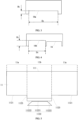
- a first distance represents a distance between the second surface 112 and the first surface 111 in the passivation regions 11a
- a second distance represents a distance between the second surface 112 and the first surface 111 in the passivated contact region 11b.
- the second distance is greater than the first distance.
- the depth of the second surface 112 in the passivation regions 11a is greater than the depth of the second surface 112 in the passivated contact regions 11b, and the depth of the second surface 112 in the passivated contact regions 11b can be set as zero.
- the above described difference between the first and second distances provides following effects: It facilitates the formation of spaced passivating contact structures 12 on the second surface 112. In addition, it can be created by removing the diffusion layers from the passivation regions 11a, and the removal of the diffusion layers from the passivation regions 11a is conductive to reducing carrier recombination. Furthermore, during the manufacturing process, recesses 16 are formed in the second surface 112 of the semiconductor substrate 11.
- the second surface 112 in the passivation regions 11a can be etched deeper, which is conducive to forming shallower recesses 16 with larger inner sizes in the passivation regions 11a, resulting in a smoother second surface 112 in the passivation regions 11a with increased light reflections.
- the difference between the second distance and the first distance is greater than 1 ⁇ m.
- the diffusion layers in the passivation regions 11a can be completely removed, thereby reducing the carrier recombination.
- the second surface 112 in the passivation regions 11a can be etched deeper, forming shallower recesses 16 with larger inner sizes, and thus forming a smoother second surface 112 in the passivation regions 11a with increased light reflections.
- the difference between the second distance and the first distance is greater than or equal to the size of each first diffusion layer 15 along the thickness direction of the semiconductor substrate 11.
- the difference between the second distance and the first distance is the depth of the second surface 112 in the passivation regions 11a relative to the second surface 112 in the passivated contact regions 11b.
- the size of each first diffusion layer 15 along the thickness direction of the semiconductor substrate 11 is the thickness of the first diffusion layer 15.
- the depth of the second surface 112 in the passivation regions 11a is greater than or equal to the thickness of the first diffusion layer 15, the first diffusion layers 15 in the passivation regions 11a can be completely removed, which is conducive to reducing the carrier recombination.
- the roughness of the second surface 112 in the passivation regions 11a can be reduced, thereby increasing the light reflections and enhancing the passivation effect.
- the second surface 112 in the passivation regions 11a can have a non-pyramidal microstructure morphology, while the second surface 112 in the passivated contact regions 11b can have a pyramidal microstructure morphology.
- the roughness of the second surface 112 in the passivation regions 11a is less than that of the second surface 112 in the passivated contact regions 11b.
- the roughness refers to surface roughness.
- the smoothness of the second surface 112 in the passivation regions 11a can be increased, thereby enhancing the mirror reflection effect.
- the smoother second surface 112 in the passivation regions 11a provides better light reflection, and thus more long-wavelength light can be reflected back into the semiconductor substrate 11, which improves the electric currents and enhances the cell efficiency.
- the reflectivity of the second surface 112 in the passivation regions 11a is greater than that of the second surface 112 in the passivated contact regions 11b. This is partly because the roughness of the second surface 112 in the passivation regions 11a is less than that of the second surface 112 in the passivated contact regions 11b, and partly because the second surface 112 in the passivation regions 11a is not covered by any passivating contact structures 12, resulting in lower absorption of long-wavelength light.
- a plurality of recesses 16 are defined in the second surface 112, including recesses 16 in the passivation regions 11a and recesses 16 in the passivated contact regions 11b. It should be noted that FIGs 2 to 4 shows microscopic schematic view of the second surface 112 of the semiconductor substrate 11, while FIGs. 1 , 5 , and 11 to 15 are more macroscopic and do not show the recesses for simplicity.
- the deepest recess 16 in the passivation regions 11a is referred to as a first recess 16a
- the deepest recess 16 in the passivated contact regions 11b is referred to as a second recess 16b.
- the depth of the first recess 16a is less than that of the second recess 16b.
- the dimension of the first recess 16a along the thickness direction of the semiconductor substrate 11 is the depth of the first recess 16a
- the dimension of the second recess 16b along the thickness direction of the semiconductor substrate 11 is the depth of the second recess 16b.
- the dimension of the first recess 16a along the thickness direction of the semiconductor substrate 11 is H 1
- the dimension of the second recess 16b along the thickness direction of the semiconductor substrate 11 is H 2 .
- the recesses are formed as a result of polishing the surface of the semiconductor substrate 11.
- the second surface 112 is further polished in the passivation regions 11a.
- the depth of the recesses 16 in the passivation regions 11a is reduced.
- the depths of most recesses 16 in the passivation regions 11a are reduced.
- the depths of the recesses 16 affect the roughness. In the same surface, the smaller the depth difference between the deepest recess 16 and the shallowest recess 16, the smaller the roughness of this surface. Therefore, the first recess 16a being shallower than the second recess 16b is conductive to making the roughness of the second surface 112 in the passivation regions 11a less than that of the second surface 112 in the passivated contact regions 11b.
- the roughness of the second surface 112 in the passivation regions 11a can be reflected by the depths of all recesses 16 in the passivation regions 11a. Furthermore, the standard deviation of the depths of all recesses 16 in the passivation regions 11a is the roughness of the second surface 112 in the passivation regions 11a.
- the roughness of the second surface 112 in the passivated contact regions 11b can be reflected by the depths of all recesses 16 in the passivated contact regions 11b. Furthermore, the standard deviation of the depths of all recesses 16 in the passivated contact regions 11b is the roughness of the second surface 112 in the passivated contact regions 11b.
- the standard deviation of the depths of all recesses 16 in the passivation regions 11a is less than the standard deviation of the depths of all recesses 16 in the passivated contact regions 11b.
- the standard deviation of the depths of all recesses 16 can be represented by the standard deviation of the depths of all recesses 16 per unit area.
- the inner size of the first recess 16a is greater than the inner size of the second recess 16b.
- the inner size of the first recess 16a is D 1
- the inner size of the second recess 16b is D 2 .
- the inner size of the recess 16 refers to the size of a cross section of the recess 16 along the direction perpendicular to the thickness direction of the semiconductor substrate 11.
- the inner size of the recess 16 is the inner diameter of the round recess.
- the inner size of the recess 16 is the side length of the square recess.
- the inner size of the recess 16 is the longest side length of the rectangular recess.
- the inner size of the recess 16 is the maximum inner size of the irregular shaped recess.
- the inner size of the recess 16 is inversely proportional to the depth of the recess 16. During the polishing process to remove the diffusion layers in the passivation regions 11a, the depths of the recesses 16 in the passivation regions 11a are reduced, and the inner sizes of the recesses 16 are increased. Thus, the inner size of the first recess 16a is greater than the inner size of the second recess 16b.
- the inner size of each recess 16 in the passivation regions 11a is greater than the inner size of the largest recess 16 (e.g., the second recess 16b) in the passivated contact regions 11b.
- the depth of each recess 16 in the passivation regions 11a is less than the depth of the deepest recess 16 (e.g., the second recess 16b) in the passivated contact regions 11b.
- the roughness of the second surface 112 in the passivation regions 11a is less than the roughness of the second surface 112 in the passivated contact regions 11b.
- the inner sizes of only a portion of the recesses 16 in the passivation region 11a are each greater than the inner size of the largest recess 16 (e.g., the second recess 16b) in the passivated contact regions 11b.
- the depths of only a portion of the recesses 16 in the passivation regions 11a are each less than the depth of the deepest recess 16 (e.g., the second recess 16b) in the passivated contact regions 11b.
- the inner size of the first recess 16a ranges from 8 ⁇ m to 40 ⁇ m.
- the inner size of the first recess 16a can be 8 ⁇ m, 15 ⁇ m, 23 ⁇ m, 30 ⁇ m, 35 ⁇ m, 40 ⁇ m, or any value between these numbers.
- the inner size of the second recess 16b ranges from 5 ⁇ m to 20 ⁇ m.
- the inner size of the second recess 16b can be 5 ⁇ m, 10 ⁇ m, 15 ⁇ m, 20 ⁇ m, or any value between these numbers.
- the depth of the first recess 16a ranges from 50 nm to 800 nm.
- the depth of the first recess 16a can be 50 nm, 200 nm, 400 nm, 600 nm, 800 nm, or any value between these numbers.
- the depth of the second recess 16b ranges from 200 nm to 1000 nm.
- the depth of the second recess 16b can be 200 nm, 400 nm, 500 nm, 700 nm, 850 nm, 1000 nm, or any value between these numbers.
- the recesses 16 of different dimensions can be formed in the second surface 112 and respectively in the passivation regions 11a and the passivated contact regions 11b, which is conducive to making the roughness of the second surface 112 in the passivation regions 11a less than the roughness of the second surface 112 in the passivated contact regions 11b.
- the dimension of the passivating contact structure 12 in the first direction X gradually decreases.
- the width of the passivating contact structure 12 gradually decreases.
- the passivating contact structure 12 has a larger surface at the side away from the semiconductor substrate 11 and a smaller surface at the side adjacent to the semiconductor substrate 11.
- the first electrode 14 can be easily in alignment with the passivating contact structure 12 during the manufacturing process, and on the other hand, the contact area between the passivating contact structure 12 and the semiconductor substrate 11 can be reduced, thereby reducing the absorption of long-wavelength light by the passivating contact structure 12.
- the passivating contact structure 12 further includes a tunnel layer 121.
- the tunnel layer 121 is disposed between the electrically conductive passivation layer 122 and the semiconductor substrate 11. Along the direction from the second surface 112 to the first surface 111, the dimension of the electrically conductive passivation layer 122 in the first direction X gradually decreases, in other words, the width of the electrically conductive passivation layer 122 gradually decreases.
- the tunnel layer 121 can be made of silicon oxide.
- the electrically conductive passivation layer 122 can be made of polysilicon, microcrystalline silicon, or silicon carbide, doped with an n-type doping element or a p-type doping element.
- the electrically conductive passivation layer 122 (e.g., a polysilicon layer) is prone to absorbing long-wavelength light.
- the above arrangement makes the surface area of the electrically conductive passivation layer 122 at the side adjacent to the semiconductor substrate 11 smaller, which is beneficial to reducing the absorption of long-wavelength light by the electrically conductive passivation layer 122, and makes the surface area of the electrically conductive passivation layer 122 at the side away from the semiconductor substrate 11 larger, which facilitates alignment with the first electrode 14 during the manufacturing process, reducing the manufacturing difficulty of the first electrode 14.
- the each passivating contact structure 12 is provided with one first electrode 14.
- the electrically conductive passivation layer 122 includes a first face adjacent to the tunnel layer 121 and a second face away from the tunnel layer 121.
- the dimension of the first face in the first direction X, the dimension of the second face in the first direction X, and the dimension of the first electrode 14 in the first direction X satisfy the following relationship: W 2 > W 1 > W 3 wherein W 1 is the dimension of the first face in the first direction X, W 2 is the dimension of the second face in the first direction X, and W 3 is the dimension of the first electrode 14 in the first direction X.
- the above arrangement makes the surface area of the electrically conductive passivation layer 122 at the side adjacent to the semiconductor substrate 11 smaller, which is beneficial to reducing the absorption of long-wavelength light by the electrically conductive passivation layer 122, and makes the surface area of the electrically conductive passivation layer 122 at the side away from the semiconductor substrate 11 larger, which facilitates alignment with the first electrode 14 during the manufacturing process, reducing the manufacturing difficulty of the first electrode 14.
- the thickness of the tunnel layer 121 ranges from 0.5 nm to 2 nm.
- the thickness of the tunnel layer 121 can be 0.5 nm, 1 nm, 1.5 nm, or 2 nm.
- the solar cell 1 further includes the dielectric layer 13; the dielectric layer 13 at least covers the second surface 112 in the passivation regions 11a, and also covers the surfaces of the passivated contact structures 12 away from the semiconductor substrate 11.
- the dielectric layer 13 is in direct contact with the second surface 112 in the passivation regions 11a. Since the roughness of the second surface 112 in the passivation regions 11a is smaller, i.e., the smoothness is better, the passivation effect of the dielectric layer 13 is improved. Additionally, covering the surfaces of the passivated contact structures 12 away from the semiconductor substrate 11 with the dielectric layer 13 enhances the passivation effect of the passivated contact structures 12.
- the thickness of the dielectric layer 13 is less than 30 nm.
- the thickness of the dielectric layer 13 can be 25 nm, 20 nm, or 10 nm.
- the dielectric layer 13 further covers the surfaces of the passivated contact structures 12 adjacent to the passivation regions 11a, i.e., the side surfaces of the passivated contact structures 12. This arrangement further enhances the passivation effect of the passivated contact structures 12.
- the second surface 112 of the semiconductor substrate 11 includes first sub-surfaces 1121, second sub-surfaces 1122, and connecting surfaces 1123.
- the first sub-surfaces 1121 are respectively located in the passivation regions 11a.
- the second sub-surfaces 1122 are respectively located in the passivation contact regions 11b.
- the connecting surfaces 1123 connect the adjacent first sub-surfaces 1121 and second sub-surfaces 1122.
- the dielectric layer 13 further covers the connecting surfaces 1123. As shown in FIG. 5 , the second sub-surface 1122 and the connecting surface 1123 together form a step. Covering the connecting surfaces 1123 with the dielectric layer 13 can provide a good passivation effect at the side surfaces of the steps.
- the second sub-surface 1122 includes a sub-contact surface 11221 and two non-contact surfaces 11222.
- the two non-contact surfaces 11222 are located at opposite sides of the sub-contact surface 11221 in the first direction X.
- the passivated contact structure 12 is in contact with the sub-contact surface 11221.
- the dielectric layer 13 further covers the non-contact surfaces 11222. As such, the non-contact surfaces 11222 of the second sub-surface 1122 can have a good passivation effect.
- a fitting groove can be formed between the passivated contact structure 12 and the non-contact surface 11222, and the dielectric layer 13 can be embedded in the fitting groove. As such, the bonding strength between the dielectric layer 13 and the semiconductor substrate 11 can be enhanced, improving the structural stability of the solar cell 1.
- the dielectric layer 13 includes one or more of aluminum oxide, silicon nitride, or silicon oxynitride.
- the dielectric layer 13 includes an aluminum oxide layer, which at least covers the second surface 112 located in the passivation regions 11a.
- the second surface 112 in the passivation regions 11a may be covered with the electrically conductive passivation layer 122 (such as a doped polysilicon layer).
- the aluminum oxide layer can provide a good passivation effect in the passivation regions 11a, which is comparable to that of a doped polysilicon layer.
- the dielectric layer 13 includes a silicon nitride layer, which at least covers the second surface 112 located in the passivation regions 11a.
- the silicon nitride layer thus provides a good passivation effect in the passivation regions 11a, thereby enhancing the performance of the solar cell 1.
- the dielectric layer 13 can be a laminated structure including at least two layers selected from an aluminum oxide layer, a silicon nitride layer, and a silicon oxynitride layer.
- the specific structure of the dielectric layer 13 is not limited in the present application.
- the electrically conductive passivation layer 122 includes a doped polysilicon layer, which is doped with an n-type doping element or a p-type doping element. As such, the passivated contact structure 12 can have a relatively good electrical conductivity.
- the doped polysilicon layer is further doped with one or more of carbon, nitrogen, and oxygen, which increases the bandgap of the layer, further reduces light absorption, and thereby improves the efficiency of the solar cell 1.
- the electrically conductive passivation layer 122 can consist solely of a doped polysilicon layer.
- the electrically conductive passivation layer 122 further includes a doped microcrystalline silicon layer, which is doped with an n-type doping element or a p-type doping element.
- the electrically conductive passivation layer 122 further includes a silicon carbide layer, which is disposed at the side of the doped polysilicon layer away from the semiconductor substrate 11. It can be understood that the silicon carbide layer can also be doped with an n-type doping element or a p-type doping element.
- the silicon carbide layer By providing the silicon carbide layer, light absorption by the electrically conductive passivation layer 122 can be reduced, which is beneficial for improving the efficiency of the solar cell 1. Additionally, during the fabrication of the first electrodes 14, the silicon carbide layer can withstand metal burning, which is conducive to reducing carrier recombination at the metal electrodes. It should be noted that during the manufacturing process, the first electrode 14 burns through the dielectric layer 13 and thus is in contact with the electrically conductive passivation layer 122, e.g., in contact with at least one of the silicon carbide layer and the doped polysilicon layer.
- the material of the tunnel layer 121 includes at least one of silicon oxide, silicon nitride, intrinsic amorphous silicon, intrinsic polysilicon, aluminum oxide, aluminum nitride, phosphorus nitride, or titanium nitride.
- the material of the electrically conductive passivation layer 122 includes at least one of polysilicon, microcrystalline silicon, or silicon carbide. Further, the electrically conductive passivation layer 122 is doped with an n-type doping element or a p-type doping element.
- the solar cell 1 further includes an emitter, one or more second electrodes, and a passivation layer.
- the emitter and the passivation layer are sequentially stacked on the first surface 111 of the semiconductor substrate 11, and the second electrodes penetrate through the passivation layer to electrically connect with the emitter.
- the first electrodes 14 are made of at least one of silver or aluminum. In an embodiment, the first electrode 14 includes both silver and aluminum. The first electrode 14 can be made from a silver-aluminum paste.
- the second electrodes are made of at least one of silver and aluminum. In an embodiment, the second electrode includes both silver and aluminum.
- the second electrode can be made from a silver-aluminum paste.
- Table 1 Comparison of Solar Cell Performance Efficiency (%) Short-circuit current I sc (mA/cm 2 ) Open-circuit voltage V oc (mV) Fill factor FF (%) Conventional TOPCon cells 24.95 41.02 730.1 83.31 Present embodiments 25.08 41.21 730.7 83.29
- the short-circuit currents of the solar cells provided in the embodiments of the present application can be increased by 0.19 mA/cm 2 and the cell efficiency can be increased by 0.13%.
- an embodiment of the present application provides a method for preparing a solar cell, which can be the solar cell 1 described in the first aspect.
- the method includes steps S10 to S40.
- the semiconductor substrate 11 includes a first surface 111 and a second surface 112 that are opposite to each other.
- the semiconductor substrate 11 includes a plurality of passivation regions 11a and a plurality of passivated contact regions 11b.
- the passivation regions 11a and the passivated contact regions 11b are alternately arranged along a first direction X.
- the first direction X is perpendicular to a thickness direction of the semiconductor substrate 11.
- the semiconductor substrate 11 can be an n-type silicon substrate.
- the semiconductor substrate 11 can be textured first.
- the second surface 112 of the semiconductor substrate 11 can be polished using an alkaline solution. After polishing, the second surface 112 of the semiconductor substrate 11 is formed to include a plurality of recesses 16.
- Each passivating contact structure 12 includes an electrically conductive passivation layer 122.
- the dielectric layer 13 at least covering the second surface 112 located in the passivation regions 11a.
- the material of the dielectric layer 13 can include one or more of silicon oxide, aluminum oxide, silicon oxynitride, or silicon nitride.
- the dielectric layer 13 can be formed by an atomic layer deposition (ALD) method. This method allows the dielectric layer 13 to be embedded in the fitting groove formed between the passivation contact structure 12 and the non-contact surface 11222.
- ALD atomic layer deposition
- the passivating contact structures 12 are formed on the second surface 112 and spaced from each other. Compared with conventional TOPCon cells, no passivating contact structures 12 are formed on the second surface 112 in the passivation regions 11a, thereby reducing the area of the second surface 112 covered by the passivating contact structures 12, decreasing the absorption of long-wavelength light by the passivating contact structures 12, thereby increasing the electric currents and enhancing solar cell efficiency.
- the passivating contact structures 12 are not thinned, and thus during the formation of the metal electrodes, the metal paste is less likely to burn through the passivating contact structures 12, so as not to adversely affect the passivation effect.
- all the materials of the passivating contact structures 12 in the passivation regions 11a are removed, which provides a larger process window and reduces preparation difficulty, making mass production more feasible.
- S20 of forming the plurality of passivating contact structures 12 on the second surface 112 specifically includes steps S21, S23, and S24.
- the material of the tunnel material layer 21 can be a dielectric material, such as silicon oxide, aluminum oxide, silicon nitride, silicon oxynitride, magnesium fluoride, amorphous silicon, polysilicon, silicon carbide, and/or titanium oxide.
- the material of the electrically conductive passivation material layer 22 can be amorphous silicon, polysilicon, microcrystalline silicon, and/or silicon carbide.
- the tunnel material layer 21 and the electrically conductive passivation material layer 22 can be prepared by using a method such as ALD, plasma enhanced chemical vapor deposition (PECVD), plasma enhanced atomic layer deposition (PEALD), or low pressure chemical vapor deposition (LPCVD).
- ALD plasma enhanced chemical vapor deposition
- PECVD plasma enhanced chemical vapor deposition
- PEALD plasma enhanced atomic layer deposition
- LPCVD low pressure chemical vapor deposition
- a patterned mask layer 232 on the electrically conductive passivation material layer 22.
- the structure formed after the process of forming the patterned mask layer 232 can be referred to FIG. 13 .
- the second surface 112 in the passivation regions 11a is exposed through the patterned mask layer 232, while the second surface 112 in the passivated contact regions 11b is shaded by the patterned mask layer 232.
- the material of the patterned mask layer 232 can be silicon oxide.
- the patterned mask layer 232 can be formed by laser etching or wet etching an oxide layer 231 formed on the surface of the electrically conductive passivation material layer 22.
- the oxide layer 231 can be simultaneously formed during step S21.
- the exposed second surface 112 of the semiconductor substrate 11 located in the passivation regions 11a can be polished using an alkaline solution, making the depth of the second surface 112 in the passivation regions 11a greater than the depth of the second surface 112 in the passivated contact regions 11b.
- the polishing process the sizes of most or even all of the recesses 16 in the passivation regions 11a can be enlarged, and the depths of the recesses 16 in the passivation regions 11a can be reduced, thereby reducing the roughness of the second surface 112 in the passivation regions 11a.
- the method further includes step S22.
- the electrically conductive passivation material layer 22 formed in step S21 can include a doping element or not include any doping elements.
- the heat treatment in step S22 can activate the doping element and further crystallize the electrically conductive passivation material layer 22.
- the oxide layer 231 can be simultaneously formed on the surface of the electrically conductive passivation material layer 22 in step S21.
- a doping source can be introduced to allow the doping element to diffuse into the electrically conductive passivation material layer 22.
- the heat treatment further crystallizes the electrically conductive passivation material layer 22.
- the method further includes step S25.
- the semiconductor substrate 11 can be polished using an alkaline solution to remove the initial diffusion layers 24 located in the passivation regions 11a.
- the initial diffusion layers 24 located in the passivation regions 11a are not removed and retained in the solar cell 1.
- S20 of forming the plurality of passivating contact structures 12 on the second surface 112 specifically includes S201 to S205.
- the material of the tunnel material layer 21 can be a dielectric material, such as silicon oxide, aluminum oxide, silicon nitride, silicon oxynitride, magnesium fluoride, amorphous silicon, polysilicon, silicon carbide, and/or titanium oxide.
- the electrically conductive passivation material layer 22 can be an amorphous silicon layer. It can be understood that the tunnel material layer 21 and the electrically conductive passivation material layer 22 can be prepared by using a method such as ALD, PECVD, PEALD, or LPCVD. Referring to FIG. 11 , an oxide layer 231 can be simultaneously formed on the surface of the electrically conductive passivation material layer 22 during step S201.
- S202 forming a patterned mask layer 232 on the electrically conductive passivation material layer 22.
- the structure formed after the process of forming the patterned mask layer 232 can be referred to FIG. 13 .
- the patterned mask layer 232 can be formed by laser etching or wet etching the oxide layer 231 formed on the surface of the electrically conductive passivation material layer 22.
- S203 performing heat treatment on the electrically conductive passivation material layer 22 thereby forming an initial diffusion layer 24.
- a thin oxide film can be formed on the surface of the electrically conductive passivation material layer 22 in the passivation regions 11a.
- the electrically conductive passivation material layer 22 formed in step S201 can include a doping element or not include any doping elements.
- the heat treatment in step S203 can activate the doping element and further crystallize the electrically conductive passivation material layer 22.
- a doping source can be introduced to allow the doping element to diffuse into the electrically conductive passivation material layer 22. The heat treatment further crystallizes the electrically conductive passivation material layer 22.
- S204 removing the tunnel material layer 21 and the electrically conductive passivation material layer 22 on the passivation regions 11a, thereby forming the passivating contact structures 12.
- the structure formed after the process of forming the passivation contact structures 12 can be referred to FIG. 14 .
- the above layers can be removed through a wet etching process using the patterned mask layer 232. It should be noted that due to the presence of the thin oxide film on the surface of the electrically conductive passivation material layer 22 in the passivation regions 11a, this oxide film is conducive to controlling the rate of wet etching, thereby improving the precision of the wet etching.
- S205 removing the initial diffusion layer 24 on the passivation regions 11a thereby forming a plurality of first diffusion layers 15.
- the semiconductor substrate 11 can be polished using an alkaline solution to remove the initial diffusion layers 24 located in the passivation regions 11a.
- the initial diffusion layers 24 located in the passivation regions 11a are not removed and retained in the solar cell 1.
- an embodiment of the present application provides a photovoltaic module, including the solar cell described in the first aspect.
- the photovoltaic module includes a plurality of solar cells 1, which can be connected in series through a welding strip, so as to collect the electric energy generated by separate solar cells 1 for subsequent transmission.
- the solar cells 1 can be arranged at intervals, or can be stacked together in an imbricated form.
- the photovoltaic module further includes an encapsulation layer and a cover plate.
- the encapsulation layer is configured to cover the surface of a group of cells.
- the cover plate is configured to cover the surface of the encapsulation layer away from the cells.
- the solar cells 1 are electrically connected into a whole piece or multiple pieces, to form a plurality of cell groups.
- the plurality of cell groups are electrically connected in series and/or in parallel. Specifically, in some embodiments, the plurality of cell groups can be electrically connected through conductive strips.
- the encapsulation layer covers the surface of the solar cells.
- the encapsulation layer can be an organic encapsulation film, such as an ethylene-vinyl acetate copolymer film, a polyethylene-octene elastomer film, or a polyethylene terephthalate film.
- the cover plate can be, for example, a glass cover plate, a plastic cover plate, or the like with a light-transmitting function.
- steps shown in the drawings can include multiple sub-steps or multiple stages, these sub-steps or stages are not necessarily performed at the same time, but may be performed at different times. These sub-steps or stages are not necessarily to be sequentially performed, but can be performed alternately or in turn with at least some of the sub-steps or stages of other steps.
Landscapes
- Photovoltaic Devices (AREA)
- Life Sciences & Earth Sciences (AREA)
- Engineering & Computer Science (AREA)
- Sustainable Development (AREA)
- Sustainable Energy (AREA)
Applications Claiming Priority (1)
| Application Number | Priority Date | Filing Date | Title |
|---|---|---|---|
| CN202410956630.XA CN118507547B (zh) | 2024-07-17 | 2024-07-17 | 太阳能电池及其制备方法、光伏组件 |
Publications (2)
| Publication Number | Publication Date |
|---|---|
| EP4478428A2 true EP4478428A2 (de) | 2024-12-18 |
| EP4478428A3 EP4478428A3 (de) | 2025-06-11 |
Family
ID=92238802
Family Applications (1)
| Application Number | Title | Priority Date | Filing Date |
|---|---|---|---|
| EP24210908.0A Pending EP4478428A3 (de) | 2024-07-17 | 2024-11-05 | Solarzelle, herstellungsverfahren dafür und fotovoltaisches modul |
Country Status (5)
| Country | Link |
|---|---|
| US (1) | US20250056918A1 (de) |
| EP (1) | EP4478428A3 (de) |
| CN (2) | CN118507547B (de) |
| AU (2) | AU2024227727B2 (de) |
| MX (1) | MX2024015851A (de) |
Cited By (2)
| Publication number | Priority date | Publication date | Assignee | Title |
|---|---|---|---|---|
| CN120076478A (zh) * | 2025-01-24 | 2025-05-30 | 西安隆基乐叶光伏科技有限公司 | 一种背接触电池和光伏组件 |
| CN120512950A (zh) * | 2025-06-12 | 2025-08-19 | 鄂尔多斯市隆基光伏科技有限公司 | 一种太阳能电池及其制造方法、光伏组件 |
Family Cites Families (30)
| Publication number | Priority date | Publication date | Assignee | Title |
|---|---|---|---|---|
| US4514582A (en) * | 1982-09-17 | 1985-04-30 | Exxon Research And Engineering Co. | Optical absorption enhancement in amorphous silicon deposited on rough substrate |
| US7851698B2 (en) * | 2008-06-12 | 2010-12-14 | Sunpower Corporation | Trench process and structure for backside contact solar cells with polysilicon doped regions |
| CN102856328B (zh) * | 2012-10-10 | 2015-06-10 | 友达光电股份有限公司 | 太阳能电池及其制作方法 |
| EP3093889B8 (de) * | 2015-05-13 | 2024-05-22 | Trina Solar Co., Ltd | Solarzelle und verfahren zur herstellung davon |
| NL2017872B1 (en) * | 2016-11-25 | 2018-06-08 | Stichting Energieonderzoek Centrum Nederland | Photovoltaic cell with passivating contact |
| CN112164728B (zh) * | 2020-10-29 | 2025-03-18 | 天合光能股份有限公司 | 图形化的钝化接触太阳能电池及其制造方法 |
| CN115700925A (zh) * | 2021-07-14 | 2023-02-07 | 天合光能股份有限公司 | 一种选择性钝化接触电池及其制备方法 |
| US12211950B2 (en) * | 2021-07-22 | 2025-01-28 | Solarlab Aiko Europe Gmbh | Passivated contact structure and solar cell comprising the same, cell assembly, and photovoltaic system |
| CN113594304B (zh) * | 2021-09-30 | 2022-05-20 | 晶科能源(海宁)有限公司 | 太阳能电池的制备方法及太阳能电池、光伏组件 |
| KR20230130266A (ko) * | 2022-03-03 | 2023-09-12 | 상라오 징코 솔라 테크놀러지 디벨롭먼트 컴퍼니, 리미티드 | 태양 전지 및 이의 제조 방법 |
| CN114744054A (zh) * | 2022-03-15 | 2022-07-12 | 西安隆基乐叶光伏科技有限公司 | 一种TOPCon电池及其制备方法 |
| CN217425526U (zh) * | 2022-04-29 | 2022-09-13 | 浙江爱旭太阳能科技有限公司 | 一种TOPCon钝化接触结构接触电阻的测试结构 |
| CN218585994U (zh) * | 2022-09-08 | 2023-03-07 | 浙江晶科能源有限公司 | 太阳能电池及光伏组件 |
| CN117673177A (zh) * | 2022-09-08 | 2024-03-08 | 浙江晶科能源有限公司 | 太阳能电池及光伏组件 |
| CN116722060A (zh) * | 2022-09-28 | 2023-09-08 | 浙江晶科能源有限公司 | 太阳能电池及光伏组件 |
| CN116722051A (zh) * | 2022-10-28 | 2023-09-08 | 浙江晶科能源有限公司 | 太阳能电池及制备方法、光伏组件 |
| CN115692548B (zh) * | 2022-11-24 | 2024-10-11 | 通威太阳能(成都)有限公司 | 太阳电池及其制备方法 |
| CN116110978B (zh) * | 2023-02-08 | 2024-05-28 | 浙江晶科能源有限公司 | 太阳能电池及其制备方法、光伏组件 |
| CN116825896A (zh) * | 2023-07-18 | 2023-09-29 | 滁州捷泰新能源科技有限公司 | 一种背面选择性钝化层topcon电池的制备方法 |
| CN220491896U (zh) * | 2023-07-24 | 2024-02-13 | 湖南红太阳新能源科技有限公司 | 一种TOPCon电池结构 |
| CN117059679A (zh) * | 2023-08-16 | 2023-11-14 | 中环新能(安徽)先进电池制造有限公司 | 一种太阳能电池的钝化接触复合层及其制备方法和应用 |
| CN120547983A (zh) * | 2023-08-30 | 2025-08-26 | 天合光能股份有限公司 | 太阳能电池及其制作方法、光伏组件及光伏系统 |
| CN117059690A (zh) * | 2023-09-15 | 2023-11-14 | 晶科能源股份有限公司 | 太阳能电池及光伏组件 |
| CN117542903A (zh) * | 2023-12-14 | 2024-02-09 | 江苏林洋太阳能有限公司 | 一种钝化接触结构及其制备方法和应用 |
| CN117497626B (zh) * | 2023-12-14 | 2024-04-23 | 天合光能股份有限公司 | 太阳能电池和太阳能电池的制造方法 |
| CN118053928A (zh) * | 2023-12-15 | 2024-05-17 | 浙江晶科能源有限公司 | 太阳能电池及光伏组件 |
| CN117832302A (zh) * | 2024-01-23 | 2024-04-05 | 隆基绿能科技股份有限公司 | 一种太阳能电池及其制备方法和电池组件 |
| CN118016745B (zh) * | 2024-04-07 | 2024-10-01 | 浙江晶科能源有限公司 | 太阳能电池及其制备方法、叠层电池及光伏组件 |
| CN118281096A (zh) * | 2024-04-08 | 2024-07-02 | 晶科能源(上饶)有限公司 | 太阳能电池及其制作方法、叠层电池及光伏组件 |
| CN121001432A (zh) * | 2024-05-17 | 2025-11-21 | 天合光能股份有限公司 | 太阳能电池及其制备方法、光伏组件、光伏系统 |
-
2024
- 2024-07-17 CN CN202410956630.XA patent/CN118507547B/zh active Active
- 2024-07-17 CN CN202411800786.5A patent/CN121368221A/zh active Pending
- 2024-10-24 US US18/925,822 patent/US20250056918A1/en active Pending
- 2024-10-29 AU AU2024227727A patent/AU2024227727B2/en active Active
- 2024-11-05 EP EP24210908.0A patent/EP4478428A3/de active Pending
- 2024-12-17 MX MX2024015851A patent/MX2024015851A/es unknown
-
2025
- 2025-04-29 AU AU2025203006A patent/AU2025203006A1/en active Pending
Cited By (2)
| Publication number | Priority date | Publication date | Assignee | Title |
|---|---|---|---|---|
| CN120076478A (zh) * | 2025-01-24 | 2025-05-30 | 西安隆基乐叶光伏科技有限公司 | 一种背接触电池和光伏组件 |
| CN120512950A (zh) * | 2025-06-12 | 2025-08-19 | 鄂尔多斯市隆基光伏科技有限公司 | 一种太阳能电池及其制造方法、光伏组件 |
Also Published As
| Publication number | Publication date |
|---|---|
| CN118507547A (zh) | 2024-08-16 |
| AU2024227727A1 (en) | 2024-11-14 |
| MX2024015851A (es) | 2025-02-10 |
| CN121368221A (zh) | 2026-01-20 |
| AU2024227727B2 (en) | 2025-04-10 |
| CN118507547B (zh) | 2024-12-31 |
| EP4478428A3 (de) | 2025-06-11 |
| AU2025203006A1 (en) | 2025-05-15 |
| US20250056918A1 (en) | 2025-02-13 |
Similar Documents
| Publication | Publication Date | Title |
|---|---|---|
| EP4287269B1 (de) | Solarzelle, herstellungsverfahren dafür, fotovoltaisches modul, und fotovoltaisches system | |
| EP4478428A2 (de) | Solarzelle, herstellungsverfahren dafür, und fotovoltaisches modul | |
| CN116722051A (zh) | 太阳能电池及制备方法、光伏组件 | |
| JP7595198B1 (ja) | 太陽電池及びその製造方法、光起電力モジュール | |
| JP7406666B2 (ja) | 太陽電池およびその製造方法、光起電力モジュール | |
| US20240363771A1 (en) | Solar cell, photovoltaic module, and photovoltaic system | |
| CN117712193A (zh) | 太阳能电池及其制备方法、光伏组件 | |
| US20250169221A1 (en) | Solar cell, photovoltaic module, and photovoltaic system | |
| JP7814575B2 (ja) | 太陽電池及び光起電力モジュール | |
| JP2025121413A (ja) | 太陽電池及びその製造方法、積層電池、並びに光起電力モジュール | |
| CN121126956A (zh) | 太阳能电池、电池组件和光伏系统 | |
| EP4694625A1 (de) | Solarzelle und fotovoltaisches modul | |
| KR100420030B1 (ko) | 태양 전지의 제조 방법 | |
| JP7777615B2 (ja) | 太陽電池及びその製造方法、光起電力モジュール | |
| KR20190041989A (ko) | 태양 전지 제조 방법 및 태양 전지 | |
| EP4539129A1 (de) | Solarzelle und fotovoltaisches modul | |
| KR101307204B1 (ko) | 태양 전지 및 그 제조 방법 | |
| KR20180064294A (ko) | 태양 전지 제조 방법 및 태양 전지 |
Legal Events
| Date | Code | Title | Description |
|---|---|---|---|
| PUAI | Public reference made under article 153(3) epc to a published international application that has entered the european phase |
Free format text: ORIGINAL CODE: 0009012 |
|
| STAA | Information on the status of an ep patent application or granted ep patent |
Free format text: STATUS: THE APPLICATION HAS BEEN PUBLISHED |
|
| AK | Designated contracting states |
Kind code of ref document: A2 Designated state(s): AL AT BE BG CH CY CZ DE DK EE ES FI FR GB GR HR HU IE IS IT LI LT LU LV MC ME MK MT NL NO PL PT RO RS SE SI SK SM TR |
|
| REG | Reference to a national code |
Ref country code: DE Ref legal event code: R079 Free format text: PREVIOUS MAIN CLASS: H01L0031035200 Ipc: H10F0010165000 |
|
| PUAL | Search report despatched |
Free format text: ORIGINAL CODE: 0009013 |
|
| AK | Designated contracting states |
Kind code of ref document: A3 Designated state(s): AL AT BE BG CH CY CZ DE DK EE ES FI FR GB GR HR HU IE IS IT LI LT LU LV MC ME MK MT NL NO PL PT RO RS SE SI SK SM TR |
|
| RIC1 | Information provided on ipc code assigned before grant |
Ipc: H10F 77/20 20250101ALI20250508BHEP Ipc: H10F 77/14 20250101ALI20250508BHEP Ipc: H10F 10/165 20250101AFI20250508BHEP |
|
| STAA | Information on the status of an ep patent application or granted ep patent |
Free format text: STATUS: REQUEST FOR EXAMINATION WAS MADE |
|
| 17P | Request for examination filed |
Effective date: 20251203 |