EP4239676A2 - Anzeigevorrichtung - Google Patents
Anzeigevorrichtung Download PDFInfo
- Publication number
- EP4239676A2 EP4239676A2 EP23156652.2A EP23156652A EP4239676A2 EP 4239676 A2 EP4239676 A2 EP 4239676A2 EP 23156652 A EP23156652 A EP 23156652A EP 4239676 A2 EP4239676 A2 EP 4239676A2
- Authority
- EP
- European Patent Office
- Prior art keywords
- sub
- layer
- pixel
- electrode
- light emitting
- Prior art date
- Legal status (The legal status is an assumption and is not a legal conclusion. Google has not performed a legal analysis and makes no representation as to the accuracy of the status listed.)
- Pending
Links
Images

















Classifications
-
- H—ELECTRICITY
- H10—SEMICONDUCTOR DEVICES; ELECTRIC SOLID-STATE DEVICES NOT OTHERWISE PROVIDED FOR
- H10H—INORGANIC LIGHT-EMITTING SEMICONDUCTOR DEVICES HAVING POTENTIAL BARRIERS
- H10H20/00—Individual inorganic light-emitting semiconductor devices having potential barriers, e.g. light-emitting diodes [LED]
- H10H20/80—Constructional details
- H10H20/85—Packages
- H10H20/851—Wavelength conversion means
-
- H—ELECTRICITY
- H10—SEMICONDUCTOR DEVICES; ELECTRIC SOLID-STATE DEVICES NOT OTHERWISE PROVIDED FOR
- H10H—INORGANIC LIGHT-EMITTING SEMICONDUCTOR DEVICES HAVING POTENTIAL BARRIERS
- H10H20/00—Individual inorganic light-emitting semiconductor devices having potential barriers, e.g. light-emitting diodes [LED]
- H10H20/80—Constructional details
- H10H20/83—Electrodes
- H10H20/831—Electrodes characterised by their shape
- H10H20/8312—Electrodes characterised by their shape extending at least partially through the bodies
-
- H—ELECTRICITY
- H10—SEMICONDUCTOR DEVICES; ELECTRIC SOLID-STATE DEVICES NOT OTHERWISE PROVIDED FOR
- H10H—INORGANIC LIGHT-EMITTING SEMICONDUCTOR DEVICES HAVING POTENTIAL BARRIERS
- H10H20/00—Individual inorganic light-emitting semiconductor devices having potential barriers, e.g. light-emitting diodes [LED]
- H10H20/80—Constructional details
- H10H20/85—Packages
- H10H20/851—Wavelength conversion means
- H10H20/8511—Wavelength conversion means characterised by their material, e.g. binder
- H10H20/8512—Wavelength conversion materials
- H10H20/8513—Wavelength conversion materials having two or more wavelength conversion materials
-
- H—ELECTRICITY
- H10—SEMICONDUCTOR DEVICES; ELECTRIC SOLID-STATE DEVICES NOT OTHERWISE PROVIDED FOR
- H10D—INORGANIC ELECTRIC SEMICONDUCTOR DEVICES
- H10D86/00—Integrated devices formed in or on insulating or conducting substrates, e.g. formed in silicon-on-insulator [SOI] substrates or on stainless steel or glass substrates
- H10D86/40—Integrated devices formed in or on insulating or conducting substrates, e.g. formed in silicon-on-insulator [SOI] substrates or on stainless steel or glass substrates characterised by multiple TFTs
- H10D86/441—Interconnections, e.g. scanning lines
-
- H—ELECTRICITY
- H10—SEMICONDUCTOR DEVICES; ELECTRIC SOLID-STATE DEVICES NOT OTHERWISE PROVIDED FOR
- H10D—INORGANIC ELECTRIC SEMICONDUCTOR DEVICES
- H10D86/00—Integrated devices formed in or on insulating or conducting substrates, e.g. formed in silicon-on-insulator [SOI] substrates or on stainless steel or glass substrates
- H10D86/40—Integrated devices formed in or on insulating or conducting substrates, e.g. formed in silicon-on-insulator [SOI] substrates or on stainless steel or glass substrates characterised by multiple TFTs
- H10D86/60—Integrated devices formed in or on insulating or conducting substrates, e.g. formed in silicon-on-insulator [SOI] substrates or on stainless steel or glass substrates characterised by multiple TFTs wherein the TFTs are in active matrices
-
- H—ELECTRICITY
- H10—SEMICONDUCTOR DEVICES; ELECTRIC SOLID-STATE DEVICES NOT OTHERWISE PROVIDED FOR
- H10H—INORGANIC LIGHT-EMITTING SEMICONDUCTOR DEVICES HAVING POTENTIAL BARRIERS
- H10H20/00—Individual inorganic light-emitting semiconductor devices having potential barriers, e.g. light-emitting diodes [LED]
- H10H20/80—Constructional details
- H10H20/81—Bodies
- H10H20/813—Bodies having a plurality of light-emitting regions, e.g. multi-junction LEDs or light-emitting devices having photoluminescent regions within the bodies
-
- H—ELECTRICITY
- H10—SEMICONDUCTOR DEVICES; ELECTRIC SOLID-STATE DEVICES NOT OTHERWISE PROVIDED FOR
- H10H—INORGANIC LIGHT-EMITTING SEMICONDUCTOR DEVICES HAVING POTENTIAL BARRIERS
- H10H20/00—Individual inorganic light-emitting semiconductor devices having potential barriers, e.g. light-emitting diodes [LED]
- H10H20/80—Constructional details
- H10H20/83—Electrodes
-
- H—ELECTRICITY
- H10—SEMICONDUCTOR DEVICES; ELECTRIC SOLID-STATE DEVICES NOT OTHERWISE PROVIDED FOR
- H10H—INORGANIC LIGHT-EMITTING SEMICONDUCTOR DEVICES HAVING POTENTIAL BARRIERS
- H10H20/00—Individual inorganic light-emitting semiconductor devices having potential barriers, e.g. light-emitting diodes [LED]
- H10H20/80—Constructional details
- H10H20/85—Packages
- H10H20/851—Wavelength conversion means
- H10H20/8514—Wavelength conversion means characterised by their shape, e.g. plate or foil
-
- H—ELECTRICITY
- H10—SEMICONDUCTOR DEVICES; ELECTRIC SOLID-STATE DEVICES NOT OTHERWISE PROVIDED FOR
- H10H—INORGANIC LIGHT-EMITTING SEMICONDUCTOR DEVICES HAVING POTENTIAL BARRIERS
- H10H20/00—Individual inorganic light-emitting semiconductor devices having potential barriers, e.g. light-emitting diodes [LED]
- H10H20/80—Constructional details
- H10H20/85—Packages
- H10H20/857—Interconnections, e.g. lead-frames, bond wires or solder balls
-
- H—ELECTRICITY
- H10—SEMICONDUCTOR DEVICES; ELECTRIC SOLID-STATE DEVICES NOT OTHERWISE PROVIDED FOR
- H10H—INORGANIC LIGHT-EMITTING SEMICONDUCTOR DEVICES HAVING POTENTIAL BARRIERS
- H10H29/00—Integrated devices, or assemblies of multiple devices, comprising at least one light-emitting semiconductor element covered by group H10H20/00
- H10H29/10—Integrated devices comprising at least one light-emitting semiconductor component covered by group H10H20/00
- H10H29/14—Integrated devices comprising at least one light-emitting semiconductor component covered by group H10H20/00 comprising multiple light-emitting semiconductor components
- H10H29/142—Two-dimensional arrangements, e.g. asymmetric LED layout
-
- H—ELECTRICITY
- H10—SEMICONDUCTOR DEVICES; ELECTRIC SOLID-STATE DEVICES NOT OTHERWISE PROVIDED FOR
- H10W—GENERIC PACKAGES, INTERCONNECTIONS, CONNECTORS OR OTHER CONSTRUCTIONAL DETAILS OF DEVICES COVERED BY CLASS H10
- H10W90/00—Package configurations
-
- H—ELECTRICITY
- H10—SEMICONDUCTOR DEVICES; ELECTRIC SOLID-STATE DEVICES NOT OTHERWISE PROVIDED FOR
- H10H—INORGANIC LIGHT-EMITTING SEMICONDUCTOR DEVICES HAVING POTENTIAL BARRIERS
- H10H20/00—Individual inorganic light-emitting semiconductor devices having potential barriers, e.g. light-emitting diodes [LED]
- H10H20/80—Constructional details
- H10H20/81—Bodies
- H10H20/819—Bodies characterised by their shape, e.g. curved or truncated substrates
-
- H—ELECTRICITY
- H10—SEMICONDUCTOR DEVICES; ELECTRIC SOLID-STATE DEVICES NOT OTHERWISE PROVIDED FOR
- H10H—INORGANIC LIGHT-EMITTING SEMICONDUCTOR DEVICES HAVING POTENTIAL BARRIERS
- H10H20/00—Individual inorganic light-emitting semiconductor devices having potential barriers, e.g. light-emitting diodes [LED]
- H10H20/80—Constructional details
- H10H20/84—Coatings, e.g. passivation layers or antireflective coatings
Definitions
- a display device includes: a plurality of sub-pixels including a first electrode and a second electrode extending in a first direction and spaced apart from each other in a second direction and a plurality of light emitting elements on and electrically connected to the first electrode and the second electrode; a bank layer extending around a region at where the light emitting elements of the sub-pixels are arranged; and a plurality of wavelength conversion layers and light transmitting layers in the region bounded by the bank layer.
- the light emitting elements overlapping the second wavelength conversion layer, the third wavelength conversion layer, and the first light transmitting layer of the second sub-pixel, respectively, may be on the same first and second electrodes.
- Each of the second wavelength conversion layer, the third wavelength conversion layer, and the first light transmitting layer of the second sub-pixel may overlap different portions of the first electrode and the second electrode.
- the second wavelength conversion layer, the third wavelength conversion layer, and the first light transmitting layer may be arranged in the first direction and may be in contact with each other.
- the second wavelength conversion layer, the third wavelength conversion layer, and the first light transmitting layer of the second sub-pixel may be arranged in the first direction, the third wavelength conversion layer may partially overlap each of the second wavelength conversion layer and the first light transmitting layer, and the third color filter layer may partially overlap each of the second color filter layer and the fourth color filter layer.
- the sub-pixels may further include a third sub-pixel including a fourth wavelength conversion layer overlapping the light emitting elements in the region bounded by the bank layer, and the fourth wavelength conversion layer may contain second wavelength conversion particles identical to those of the third wavelength conversion layer.
- the sub-pixels may further include a fourth sub-pixel including a second light transmitting layer overlapping the light emitting elements in the region bounded by the bank layer.
- the light transmitting layer in the first sub-pixel may overlap the first light emitting element of the first sub-pixel, and the light transmitting layer in the second sub-pixel may overlap each of the first light emitting element, the second light emitting element, and the third light emitting element of the second sub-pixel.
- the first light emitting element, the second light emitting element, and the third light emitting element of the second sub-pixel may be spaced apart from each other in the first direction, the bank layer may extend around each of a region at where the first light emitting element is arranged, a region at where the second light emitting element is arranged, and a region at where the third light emitting element is arranged in the second sub-pixel, and the light transmitting layer in the second sub-pixel may be in the region bounded by the bank layer in the second sub-pixel.
- the sub-pixels SPXn are illustrated as having emission areas EMA that are substantially identical in size, the disclosure is not limited thereto.
- the emission areas EMA of the sub-pixels SPXn may have different sizes according to a color or wavelength band of light emitted from the light emitting element ED disposed in each sub-pixel.
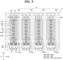
- the first barrier wall BP1 and the second barrier wall BP2 may be alternately disposed along the second direction DR2 and may be disposed in an island-like pattern in the display area DPA.
- the plurality of light emitting elements ED may be arranged between the first barrier wall BP1 and the second barrier wall BP2.
- the electrodes RME may be in direct contact with the third conductive layer through the electrode contact holes CTD and CTS at the portions overlapping the bank layer BNL between the emission area EMA and the sub-region SA.
- the first electrode contact hole CTD may be formed in an area in which the bank layer BNL and the first electrode RME1 overlap
- the second electrode contact hole CTS may be formed in an area in which the bank layer BNL and the second electrode RME2 overlap.
- the first electrode RME1 may be in contact with the first conductive pattern CDP1 through the first electrode contact hole CTD penetrating the via layer VIA and the first passivation layer PV1.
- the plurality of electrodes RME may include a conductive material having high reflectivity.
- the electrodes RME may include a metal, such as silver (Ag), copper (Cu), or aluminium (Al), or may include an alloy including aluminium (Al), nickel (Ni), lanthanum (La), or the like.
- the electrodes RME may have a structure in which a metal layer, such as titanium (Ti), molybdenum (Mo), and niobium (Nb), and the alloy are stacked.
- the bank layer BNL may have a height. In some embodiments, a top surface of the bank layer BNL may be higher than that of the barrier walls BP1 and BP2, and the thickness of the bank layer BNL may be equal to or greater than that of the barrier walls BP1 and BP2.
- the bank layer BNL may prevent ink from overflowing to adjacent sub-pixels SPXn during an inkjet printing process during the manufacturing process of the display device 10.
- the bank layer BNL may include an organic insulating material, such as polyimide.
- the light emitting elements ED may be arranged in the emission area EMA.
- the light emitting elements ED may be disposed on the first insulating layer PAS1 between the barrier walls BP1 and BP2.
- the light emitting element ED may be disposed such that one direction in which the light emitting element ED extends is parallel to the top surface of the first substrate SUB.
- the light emitting element ED may include a plurality of semiconductor layers arranged along one direction in which the light emitting element ED extends, and the plurality of semiconductor layers may be sequentially arranged along the direction parallel to the top surface of the first substrate SUB.
- the disclosure is not limited thereto, and the plurality of semiconductor layers of the light emitting element ED may be arranged in a direction perpendicular to the first substrate SUB when the light emitting element ED has another structure.
- the sub-pixels SPXn emitting different color light may include the light emitting elements ED emitting light of the same color.
- the first sub-pixel SPX1, the second sub-pixel SPX2, the third sub-pixel SPX3, and the fourth sub-pixel SPX4 may include the same type of light emitting elements ED.
- the light emitted from the emission areas EMA of the sub-pixels SPXn may be the same color light (e.g., blue light of the third color).
- the blue light of the third color emitted from the light emitting element ED may be converted to light of another color by the color control structures disposed thereon. A detailed description thereof will be given later with reference to other drawings.
- the plurality of connection electrodes CNE may be disposed on the plurality of electrodes RME and the barrier walls BP1 and BP2.
- the first connection electrode CNE1 may be disposed on the first electrode RME1 and the first barrier wall BP1.
- the first connection electrode CNE1 may partially overlap the first electrode RME1 and may be disposed across the emission area EMA and the sub-region SA over the bank layer BNL.
- the second connection electrode CNE2 may be disposed on the second electrode RME2 and the second barrier wall BP2.
- the second connection electrode CNE2 may partially overlap the second electrode RME2 and may be disposed across the emission area EMA and the sub-region SA over the bank layer BNL.
- connection electrodes CNE may be in contact with the electrode RME through the contact portions CT1 and CT2 disposed in the sub-region SA.
- the first connection electrode CNE1 may be in contract with the first electrode RME1 through the first contact portion CT1 penetrating the first insulating layer PAS1, the second insulating layer PAS2, and the third insulating layer PAS3 in the sub-region SA.
- the second connection electrode CNE2 may be in contact with the second electrode RME2 through the second contact portion CT2 penetrating the first insulating layer PAS1 and the second insulating layer PAS2 in the sub-region SA.
- Each of the connection electrodes CNE may be electrically connected to the third conductive layer through each of electrodes RME.
- the first connection electrode CNE1 may be electrically connected to the first transistor T1 so that the first power voltage may be applied to the first connection electrode CNE1, and the second connection electrode CNE2 may be electrically connected to the second voltage line VL2 so that the second power voltage may be applied to the second connection electrode CNE2.
- Each connection electrode CNE may be in contact with the light emitting element ED in the emission area EMA to transmit the power voltage to the light emitting element ED.
- the plurality of connection electrodes CNE may be in direct contact with the third conductive layer and may be electrically connected to the third conductive layer through patterns other than the electrodes RME.
- connection electrodes CNE may include a conductive material.
- the connection electrodes CNE may include ITO, IZO, ITZO, aluminium (Al), or the like.
- connection electrodes CNE may include a transparent conductive material, and light emitted from the light emitting element ED may pass through the connection electrodes CNE to be emitted.
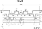
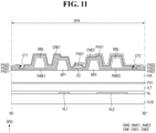
- the shapes of the barrier walls BP1 and BP2, the electrodes RME1 and RME2, the bank layer BNL, the light emitting elements ED, and the connection electrodes CNE1 and CNE2 disposed in each sub-pixel SPXn are illustrated in a simplified manner, and only the first insulating layer PAS1 from among the insulating layers PAS1, PAS2 and PAS3 is illustrated. A detailed arrangement structure thereof will be understood with reference to FIGS. 10 and 11 .
- the upper bank layer UBN may be disposed on the fourth insulating layer PAS4 to overlap the bank layer BNL.
- the upper bank layer UBN may include portions extending in the first and second directions DR1 and DR2 to be arranged in (or to form) a grid pattern.
- the upper bank layer UBN may surround, in a plan view, the emission area EMA or a portion where the light emitting elements ED are disposed.
- the upper bank layer UBN may form an area in which the color control structures TPL and WCL are disposed.
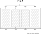
- the light transmitting layer TPL may include a first light transmitting layer TPL1 disposed in the second sub-pixel SPX2 and a second light transmitting layer TPL2 disposed in the fourth sub-pixel SPX4.
- the first wavelength conversion layer WCL1 may be disposed in the first light transmitting area TA1
- the second wavelength conversion layer WCL2 may be disposed in the first sub light transmitting area STA1 of the second light transmitting area TA2.
- the third wavelength conversion layer WCL3 may be disposed in the second sub light transmitting area STA2 of the second light transmitting area TA2
- the fourth wavelength conversion layer WCL4 may be disposed in the third light transmitting area TA3 of the third sub-pixel SPX3.
- the first wavelength conversion layer WCL1 and the second wavelength conversion layer WCL2 may include a first base resin BRS1 and a first wavelength conversion material WCP1 disposed in the first base resin BRS1.
- the third wavelength conversion layer WCL3 and the fourth wavelength conversion layer WCL4 may include a second base resin BRS2 and a second wavelength conversion material WCP2 disposed in the second base resin BRS2.
- the wavelength conversion layer WCL may transmit the blue light of the third color incident from the light emitting element ED while converting (e.g., configured to convert) the wavelength thereof.
- the wavelength conversion layer WCL may further include a scatterer SCP in (e.g., suspended in) each base resin, and the scatterer SCP may increase wavelength conversion efficiency.
- the first light transmitting layer TPL1 and the second light transmitting layer TPL2 may include a third base resin BRS3 and a scatterer SCP disposed in the third base resin BSR3.
- the light transmitting layer TPL may transmit the blue light of the third color incident from the light emitting element ED while maintaining the wavelength thereof.
- the scatterer SCP of the light transmitting layer TPL may control an emission path of the light emitted through the light transmitting layer TPL.
- the light transmitting layer TPL may not include a wavelength conversion material.
- the first wavelength conversion material WCP1 may convert the blue light of the third color into the red light of the first color
- the second wavelength conversion material WCP2 may convert the blue light of the third color into the green light of the second color.
- the first wavelength conversion material WCP1 and the second wavelength conversion material WCP2 may be quantum dots, quantum bars, phosphors or the like. Examples of the quantum dot may include group IV nanocrystals, group II-VI compound nanocrystals, group III-V compound nanocrystals, group IV-VI nanocrystals, and a combination thereof.
- the color control structures TPL and WCL may be formed by an inkjet printing process or a photoresist process.
- the color control structures TPL and WCL may be formed by a process of spraying or coating materials thereof into the area surrounded by the upper bank layer UBN and performing drying or exposure and development.
- the color control structures TPL and WCL are formed by an inkjet printing process is illustrated, and the top surfaces of the layers of the color control structures TPL and WCL are not flat and the edges adjacent to the upper bank layer UBN may be higher than the central portions is shown.
- the disclosure is not limited thereto.
- the first wavelength conversion layer WCL1 and the fourth wavelength conversion layer WCL4 may be disposed in the first sub-pixel SPX1 and the third sub-pixel SPX3, respectively.
- the first wavelength conversion layer WCL1 may be disposed on the first emission area EMA1 of the first sub-pixel SPX1 and may be disposed in the area in which the bank layer BNL and the upper bank layer UBN surround, in a plan view, the first sub-pixel SPX1.
- the fourth wavelength conversion layer WCL4 may be disposed on the third emission area EMA3 of the third sub-pixel SPX3 and may be disposed in the area in which the bank layer BNL and the upper bank layer UBN surround, in a plan view, the third sub-pixel SPX3.
- the light emitting elements ED disposed in each sub-pixel SPXn may be disposed to overlap the color control structures TPL and WCL thereon, and the light emitted from the light emitting elements ED may be incident on the color control structures TPL and WCL.
- the first type sub-pixels light of a specific color or light of a specific wavelength band may be emitted from the light transmitting area TA depending on types of the color control structures TPL and WCL disposed therein.
- different color or light of different wavelength bands may be simultaneously emitted, or mixed light thereof, may be emitted from the transmitting area TA depending on the two or more different types of color control structures TPL and WCL.
- the light incident on the first wavelength conversion layer WCL1 may be converted to red light
- the light incident on the fourth wavelength conversion layer WCL4 may be converted to green light
- the light incident on the second light transmitting layer TPL2 may be transmitted as the same blue light without wavelength conversion.
- the first sub-pixel SPX1, the third sub-pixel SPX3, and the fourth sub-pixel SPX4 include the light emitting elements ED emitting light of the same color, they may emit light of different colors depending on the arrangement of the color control structures TPL and WCL disposed thereon.
- Some of the light emitting elements ED disposed in the second sub-pixel SPX2 may be disposed to overlap the second wavelength conversion layer WCL2, some others thereof may be disposed to overlap the third wavelength conversion layer WCL3, yet some others thereof may be disposed to overlap the first light transmitting layer TPL1.
- the light emitted from some of the light emitting elements ED of the second sub-pixel SPX2 may be incident on the second wavelength conversion layer WCL2, the light emitted from some other light emitting elements ED may be incident on the third wavelength conversion layer WCL3, and the light emitted from yet some other light emitting elements ED may be incident on the first light transmitting layer TPL1.
- the first capping layer CPL1 may be disposed to cover the color control structures TPL and WCL and may be disposed along the stepped portion formed by them.
- the color control structures TPL and WCL may be disposed to fill the area surrounded, in a plan view, by the upper bank layer UBN, and the first capping layer CPL1 may be disposed to extend from top surfaces of the color control structures TPL and WCL to a top surface of the upper bank layer UBN.
- the low refractive layer LRL may be disposed on the first capping layer CPL1.
- the low refractive layer LRL is an optical layer for recycling the light having transmitted the color control structures TPL and WCL and may improve the light emission efficiency and the color purity of the display device 10.
- the low refractive layer LRL may be made of an organic material having a low refractive index and may compensate the stepped portion formed by the color control structures TPL and WCL and the upper bank layer UBN.
- the color filter layer CFL may include a first color filter layer CFL1 disposed in the first sub-pixel SPX1, second to fourth color filter layers CFL2, CFL3, and CFL4 disposed in the second sub-pixel SPX2, a fifth color filter layer CFL5 disposed in the third sub-pixel SPX3, and a sixth color filter layer CFL6 disposed in the fourth sub-pixel SPX4.
- the color filter layer CFL may be disposed in an island-like pattern to correspond to the light transmitting area TA or the emission area EMA. However, the disclosure is not limited thereto.
- the color filter layer CFL may be disposed across the plurality of light transmitting areas TA or emission areas EMA to form a linear pattern.
- the color patterns CP1, CP2, and CP3 may be disposed on the planarization layer PNL or the color filter layer CFL.
- the color patterns CP1, CP2, and CP3 may be made of the same material as that of the color filter layer CFL and disposed in the light blocking area BA.
- the color patterns CP1, CP2, and CP3 and different color filter layers CFL may be stacked, and light transmission may be blocked in the area at where they are stacked.
- the first color pattern CP1 may be made of the same material as those of the first color filter layer CFL1 and the second color filter layer CFL2 and disposed in the light blocking area BA.
- the first color pattern CP1 may be directly disposed on the planarization layer PNL in the light blocking area BA and may not be disposed in the first light transmitting area TA1 of the first sub-pixel SPX1 and the light blocking area BA adjacent to the first sub light transmitting area STA1 of the second sub-pixel SPX2.
- the color patterns CP1, CP2, and CP3 may not be disposed between the sub light transmitting areas STA1, STA2, and STA3 of the second sub-pixel SPX2, or at the portions where different color filter layers CFL are in contact with each other or overlap.
- the overcoat layer OC may be disposed on the color filter layer CFL and the color patterns CP1, CP2, and CP3.
- the overcoat layer OC may be disposed in the entire display area DPA and may be partially disposed in the non-display area NDA.
- the overcoat layer OC may protect the members containing an organic insulating material and arranged in the display area DPA from the outside.
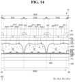
- the light emitting element ED disposed in the first sub-pixel SPX1 may emit the blue light of the third color, and the light may be incident on the first wavelength conversion layer WCL1 while transmitting through the fourth insulating layer PAS4.
- the first base resin BRS1 of the first wavelength conversion layer WCL1 may be made of a transparent material, and some of the light may transmit through the first base resin BRS1 to be incident on the first capping layer CPL1 disposed thereon. However, at least some of the light may be incident on the scatterer SCP and the first wavelength conversion material WCP1 arranged in the first base resin BRS1. The light may be scattered and wavelength converted, and may then be incident as red light on the first capping layer CPL1.
- the light emitted from the light emitting element ED disposed in the third sub-pixel SPX3 may be emitted as the green light while transmitting through the fourth insulating layer PAS4, the fourth wavelength conversion layer WCL4, the first capping layer CPL1, the low refractive layer LRL, the second capping layer CPL2, the planarization layer PNL, and the fifth color filter layer CFL5.
- the light incident on the first capping layer CPL1 may be incident on the sixth color filter layer CFL6 while transmitting through the low refractive layer LRL, the second capping layer CPL2, and the planarization layer PNL, and the transmission of other light except the blue light may be blocked by the sixth color filter layer CFL6. Accordingly, the fourth sub-pixel SPX4 may emit the blue light.
- the light emitting element ED disposed in the second sub-pixel SPX2 may emit blue light of the third color, and the blue light of the third color may be incident on any one of the second wavelength conversion layer WCL2, the third wavelength conversion layer WCL3, and the first light transmitting layer TPL1 while transmitting through the fourth insulating layer PAS4.
- the light may be incident on different color filter layers CFL while transmitting through the second wavelength conversion layer WCL2, the third wavelength conversion layer WCL3, the first light transmitting layer TPL1, the first capping layer CPL1, the low refractive layer LRL, the second capping layer CPL2, and the planarization layer PNL.
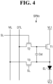
- the second sub-pixel SPX2 may have the 3T1C pixel circuit structure so that the light emitting elements ED may emit light in response to the same driving signal, and the second sub-pixel SPX2 may emit different color light simultaneously or may emit mixed light thereof.
- the arrangement of the electrodes RME and the connection electrodes CNE disposed in the sub-pixels SPXn may be the same and the same type of light emitting elements ED may be disposed therein, but the pixels PX may emit white light in addition to simultaneously emitting red light, green light, and blue light.
- one pixel PX may include four sub-pixels SPXn and may include the first type sub-pixel (e.g., the first sub-pixel, the third sub-pixel, and the fourth sub-pixel) emitting light of one color and the second type sub-pixel emitting light of two or more colors or mixed light.
- the structures of the electrode RME and the light emitting elements ED may be the same, but the arrangement of the color control structures TPL and WCL disposed thereon may be different so that different color light may be emitted.
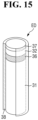
- FIG. 15 is a schematic view of a light emitting element according to one embodiment.
- the light emitting element ED may be a light emitting diode.
- the light emitting element ED may be an inorganic light emitting diode that has a nanometer or micrometer size and is made of an inorganic material.
- the light emitting element ED may be aligned between two electrodes exhibiting polarity when an electric field is formed in a specific direction between them.
- the light emitting element ED may have a shape elongated in one direction.
- the light emitting element ED may have a shape of a cylinder, a rod, a wire, a tube, or the like.
- the shape of the light emitting element ED is not limited thereto, and the light emitting element ED may have a polygonal prism shape, such as a regular cube, a rectangular parallelepiped, and a hexagonal prism, or may have various shapes, such as a shape elongated in one direction and having an outer surface partially inclined.
- the light emitting element ED may include a semiconductor layer doped with any conductivity type (e.g., p-type or n-type) dopant.
- the semiconductor layer may emit light of a specific wavelength band by receiving an electrical signal applied from an external power source.
- the light emitting element ED may include a first semiconductor layer 31, a second semiconductor layer 32, a light emitting layer 36, an electrode layer 37, and an insulating film 38.
- the first semiconductor layer 31 and the second semiconductor layer 32 are each configured as one layer, the disclosure is not limited thereto.
- the first semiconductor layer 31 and the second semiconductor layer 32 may further include a greater number of layers, such as a cladding layer or a tensile strain barrier reducing (TSBR) layer.
- the light emitting element ED may further include another semiconductor layer disposed between the first semiconductor layer 31 and the light emitting layer 36 or between the second semiconductor layer 32 and the light emitting layer 36.
- the light emitting layer 36 is disposed between the first semiconductor layer 31 and the second semiconductor layer 32.
- the light emitting layer 36 may include a material having a single or multiple quantum well structure. When the light emitting layer 36 includes a material having a multiple quantum well structure, a plurality of quantum layers and well layers may be alternately stacked.
- the light emitting layer 36 may emit light by the coupling of electron-hole pairs according to an electrical signal applied through the first semiconductor layer 31 and the second semiconductor layer 32.
- the light emitting layer 36 may include a material such as AlGaN, AlGaInN, or InGaN.
- the quantum layer may include a material such as AlGaN or AlGaInN
- the well layer may include a material such as GaN or AlInN.
- the electrode layer 37 may be an ohmic connection electrode. However, the disclosure is not limited thereto, and it may be a Schottky connection electrode.
- the light emitting element ED may include at least one electrode layer 37.
- the light emitting element ED may include one or more electrode layers 37, but the disclosure is not limited thereto, and the electrode layer 37 may be omitted in some embodiments.
- the electrode layer 37 may reduce the resistance between the light emitting element ED and the electrode or connection electrode.
- the electrode layer 37 may include a conductive metal.
- the electrode layer 37 may include at least one of aluminium (Al), titanium (Ti), indium (In), gold (Au), silver (Ag), ITO, IZO, or ITZO.
- an outer surface of the insulating film 38 may be surface-treated.
- the light emitting elements ED may be aligned in such a way of spraying the ink in which the light emitting elements ED are dispersed on the electrodes.
- the surface of the insulating film 38 may be treated to have a hydrophobic property or hydrophilic property to keep the light emitting elements ED in the dispersed state without being aggregated with other adjacent light emitting elements ED in the ink.
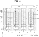
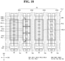
- FIG. 16 is a plan view illustrating wavelength conversion layers and light transmitting layers disposed in one pixel of a display device according to another embodiment.
- FIG. 17 is a cross-sectional view taken along the line N5-N5' of FIG. 16 and is a cross-sectional view of the second sub-pixel SPX2 of FIG. 16 taken along the first direction DR1.
- the second wavelength conversion layer WCL2, the third wavelength conversion layer WCL3, and the first light transmitting layer TPL1 of the second sub-pixel SPX2 may be disposed in contact with each other without being spaced apart from each other.
- the second wavelength conversion layer WCL2, the third wavelength conversion layer WCL3, and the first light transmitting layer TPL1, which are the color control structures disposed in the second sub-pixel SPX2, may be disposed to fill the area surrounded, in a plan view, by the bank layer BNL and the upper bank layer UBN.
- the second wavelength conversion layer WCL2, the third wavelength conversion layer WCL3, and the first light transmitting layer TPL1 of the second sub-pixel SPX2 may be arranged to partially overlap each other.
- the second wavelength conversion layer WCL2, the third wavelength conversion layer WCL3, and the first light transmitting layer TPL1, which are the color control structures disposed in the second sub-pixel SPX2, may be arranged to fill the area surrounded, in a plan view, by the bank layer BNL and the upper bank layer UBN.
- the second wavelength conversion layer WCL2, the third wavelength conversion layer WCL3, and the first light transmitting layer TPL1 may be disposed to partially overlap other adjacent color control structures.
- the second wavelength conversion layer WCL2, the third wavelength conversion layer WCL3, and the first light transmitting layer TPL1, which are the structures that facilitate emission of mixed light of red light, green light, and blue light from the second light transmitting area TA2 of the second sub-pixel SPX2, may be disposed to partially overlap each other.
- the second sub-pixel SPX2 of the display device 10_3 may include different color control structures disposed in the areas divided by the upper bank layer UBN, and the light emitted from the light emitting elements ED may be simultaneously emitted from the sub light transmitting areas STA1, STA2, and STA3 of the second sub-pixel SPX2 through the color control structures and the color filter layer CFL.
- different color light may be simultaneously emitted from different sub light transmitting areas STA1, STA2, and STA3, and the second sub-pixel SPX2 may display a mixed color light.
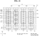
- FIG. 23 is a plan view schematically illustrating emission areas disposed in one pixel of a display device according to another embodiment
- FIG. 24 is a plan view illustrating schematic arrangement of light transmitting layers disposed in one pixel of the display device shown in FIG. 23 .
- light emitted from the emission areas EMA1, EMA2, EMA3, and EMA4 of the sub-pixels SPXn may have different colors or different central wavelength bands.
- the light emitted from the emission area EMA may be emitted from the light transmitting area TA through the light transmitting layers TPL disposed in the sub-pixel SPXn without color conversion or wavelength conversion.
- the sub-pixels SPXn of each pixel PX may emit different color light from the light transmitting areas TA.
- the light emitting element ED disposed in the third sub-pixel SPX3 may emit green light of the second color, and the light may be emitted as the green light from the third light transmitting area TA3 through the light transmitting layer TPL disposed in the third sub-pixel SPX3.
- the light emitting element ED disposed in the fourth sub-pixel SPX4 may emit blue light of the third color, and the light may be emitted as the blue light from the fourth light transmitting area TA4 through the light transmitting layer TPL disposed in the fourth sub-pixel SPX4.
- the green light of the second color may be emitted from the third emission area EMA3 of the third sub-pixel SPX3, and the green light of the second color may also be emitted from the third light transmitting area TA3.
- the blue light of the third color may be emitted from the fourth emission area EMA4 of the fourth sub-pixel SPX4, and the blue light of the third color may also be emitted from the fourth light transmitting area TA4.
- the plurality of light emitting elements ED emitting light of different colors may be disposed in the second sub-pixel SPX2. Some of the light emitting elements ED of the second sub-pixel SPX2 may emit red light of the first color, some others thereof may emit green light of the second color, and yet some others thereof may emit blue light of the third color.
- the second emission area EMA2 of the second sub-pixel SPX2 may include a plurality of sub-emission areas SEA1, SEA2, and SEA3 in which different color light is emitted.
- the light emitting elements ED emitting red light of the first color may be disposed in the first sub-emission area SEA1 to emit red light
- the light emitting elements ED emitting green light of the second color may be disposed in the second sub-emission area SEA2 to emit green light
- the light emitting elements ED emitting blue light of the third color may be disposed in the third sub-emission area SEA3 to emit blue light.
- the second emission area EMA2 includes the plurality of sub-emission areas SEA1, SEA2, and SEA3, the sub-emission areas SEA1, SEA2, and SEA3 may not be distinguished by physical interfaces.
- the plurality of sub-emission areas SEA1, SEA2, and SEA3 illustrated in the drawing which are the areas distinguished to correspond to different electrodes (shown in, e.g., FIGS. 25 and 26 ) disposed in the second sub-pixel SPX2, to be described later, may form one second emission area EMA2 without being physically distinguished in the second sub-pixel SPX2 of the display device 10_4.
- the second emission area EMA2 may include the sub-emission areas SEA1, SEA2, and SEA3 that are physically spaced apart from each other depending on the structure of the bank layer BNL disposed in the second sub-pixel SPX2.
- each of the pixels PX may include, in addition to the sub-pixels (e.g., the first sub-pixel SPX1, the third sub-pixel SPX3, and the fourth sub-pixel SPX4) emitting different color light, the sub-pixel (e.g., the second sub-pixel SPX2) emitting different color light simultaneously or emitting mixed light thereof. This may vary depending on the arrangement of the light emitting elements ED of the sub-pixels SPXn of the display device 10_4 and the arrangement of the color control structures.
- the sub-pixels e.g., the first sub-pixel SPX1, the third sub-pixel SPX3, and the fourth sub-pixel SPX4
- the sub-pixel e.g., the second sub-pixel SPX2
- This may vary depending on the arrangement of the light emitting elements ED of the sub-pixels SPXn of the display device 10_4 and the arrangement of the color control structures.
- FIG. 25 is a plan view illustrating one pixel of a display device according to one embodiment
- FIG. 26 is a plan view illustrating a second sub-pixel shown in FIG. 25
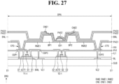
- FIG. 27 is a cross-sectional view taken along the line E1-E1' of FIG. 26
- FIG. 28 is a cross-sectional view taken along the line E2-E2' of FIG. 26
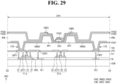
- FIG. 29 is a cross-sectional view taken along the line E3-E3' in FIG. 26
- FIGS. 27 to 29 illustrate cross sections across both ends (e.g., opposite ends) of different light emitting elements ED (e.g., ED1, ED2, and ED3) disposed in the second sub-pixel SPX2.
- ED light emitting elements
- Each of the pixels PX of the display device 10_4 may include the plurality of sub-pixels SPXn.
- one pixel PX may include the first sub-pixel SPX1, the second sub-pixel SPX2, the third sub-pixel SPX3, and the fourth sub-pixel SPX4. A description thereof is the same as described above.
- Each sub-pixel SPXn of the display device 10 may include an emission area EMA and a non-emission area.
- the emission area EMA may be an area in which the light emitting element ED is disposed to emit light of a specific wavelength band.
- the non-emission area may be a region in which the light emitting element ED is not disposed and a region from which light is not emitted because light emitted from the light emitting element ED does not reach it.
- Each sub-pixel SPXn may further include a sub-region SA disposed in the non-emission area.
- the display device 10_4 may include a plurality of electrodes RME (e.g., RME1, RME2, RME3, RME4, RME5, and RME6), the barrier walls BP1 and BP2, the bank layer BNL, and the light emitting elements ED (e.g., ED1, ED2, and ED3), and connection electrodes CNE (e.g., CNE1, CNE2, CNE3, CNE4, CNE5, and CNE6).
- RME e.g., RME1, RME2, RME3, RME4, RME5, and RME6
- the plurality of barrier walls BP1 and BP2 may be disposed in the emission area EMA of each sub-pixel SPXn.
- the barrier walls BP1 and BP2 may extend in the first direction DR1 and may be disposed to be spaced apart from each other in the second direction DR2.
- the barrier walls BP1 and BP2 may include a first barrier wall BP1 and a second barrier wall BP2 spaced apart from each other in the second direction DR2 in the emission area EMA of each sub-pixel SPXn.
- the plurality of light emitting elements ED may be arranged between the first barrier wall BP1 and the second barrier wall BP2.
- each pixel PX may include the first electrode RME1 and the second electrode RME2 disposed in each of the first sub-pixel SPX1, the third sub-pixel SPX3, and the fourth sub-pixel SPX4.
- the first electrode RME1 is located on the left side in the drawings with respect to the center of the emission area EMA
- the second electrode RME2 is located on the right side in the drawings with respect to the center of the emission area EMA while being spaced apart from the first electrode RME1 in the second direction DR2.
- a first electrode RME1 may be disposed on the first barrier wall BP1
- a second electrode RME2 may be disposed on the second barrier wall BP2.
- the first electrode RME1 and the second electrode RME2 may be partially arranged in the corresponding sub-pixel SPXn and the sub-region SA over the bank layer BNL.
- the first electrode RME1 and the second electrode RME2 of different sub-pixels SPXn may be spaced or separated from each other at the separation portion ROP disposed in the sub-region SA of any one sub-pixel SPXn.
- the second sub-pixel SPX2 may include, in addition to the first electrode RME1 and the second electrode RME2, a third electrode RME3, a fourth electrode RME4, a fifth electrode RME5, and a sixth electrode RME6 spaced apart from them in the first direction DR1.
- the first to sixth electrodes RME1, RME2, RME3, RME4, RME5, and RME6 disposed in the second sub-pixel SPX2 may have a relatively short length extending in the first direction DR1 compared to the electrodes RME disposed in other sub-pixels SPXn.
- the electrodes RME1, RME2, RME3, RME4, RME5, and RME6 of the second sub-pixel SPXn may be separated to be spaced apart from each other in the emission area EMA.
- the third electrode RME3 and the fourth electrode RME4 may be disposed at the central portion or the central area of the emission area EMA to be spaced apart from the first electrode RME1 and the second electrode RME2 in the first direction DR1, respectively.
- the third electrode RME3 and the fourth electrode RME4 may include portions extending in the first direction DR1 and portions that are bent therefrom in the second direction DR2 to overlap the bank layer BNL.
- the portions of the third electrode RME3 and the fourth electrode RME4 extending in the first direction DR1 may be disposed on the first barrier wall BP1 and the second barrier wall BP2, respectively, and may be electrically connected to the third conductive layer through the first electrode contact hole CTD and the second electrode contact hole CTS formed at the portions overlapping the bank layer BNL.
- the third electrode RME3 may be electrically connected to a first-second transistor T1_2 through the first electrode contact hole CTD, and the fourth electrode RME4 may be electrically connected to the second voltage line VL2 through the second electrode contact hole CTS.
- the fifth electrode RME5 and the sixth electrode RME6 may be electrically connected to the third conductive layer through the first electrode contact hole CTD and the second electrode contact hole CTS formed at the portions overlapping the bank layer BNL.
- the fifth electrode RME5 may be electrically connected to a first-third transistors T1_3 through the first electrode contact hole CTD, and the sixth electrode RME6 may be electrically connected to the second voltage line VL2 through the second electrode contact hole CTS.
- the two electrodes RME1 and RME2 may be electrically connected to the first transistor T1 and the second voltage line VL2, respectively, whereas different pairs of electrodes RME1, RME2, RME3, RME4, RME5, and RME6 of the second sub-pixel SPX2 may be electrically connected to different first transistors (e.g., the first-first to first-third transistors T1_1, T1_2, and T1_3).
- the light emitting elements ED disposed in the plurality of sub-pixels SPXn may emit different color light
- the light emitting elements ED emitting different color light may be disposed in the second sub-pixel SPX2.
- the light emitting elements ED emitting different color light may be disposed on different pairs of electrodes RME1, RME2, RME3, RME4, RME5, and RME6, and they may be individually driven.
- the second sub-pixel SPX2 of the display device 10_4 may have a 9T3C pixel circuit structure.
- the bank layer BNL may be disposed to surround the plurality of sub-pixels SPXn, the emission area EMA, and the sub-region SA.
- the bank layer BNL may be disposed at the boundary between the sub-pixels SPXn adjacent in the first direction DR1 and the second direction DR2 and may also be disposed at the boundary between the emission area EMA and the sub-region SA.
- the bank layer BNL may include portions extending in the first direction DR1 and the second direction DR2 in a plan view to be arranged in a grid pattern over the entire surface of the display area DPA.
- the plurality of light emitting elements ED1, ED2, and ED3 may be disposed in the emission area EMA of each sub-pixel SPXn.
- the light emitting elements ED may be disposed between the barrier walls BP1 and BP2 and may be arranged to be spaced apart from each other in the first direction DR1.
- the first light emitting element ED1, the second light emitting element ED2, and the third light emitting element ED3 of the second sub-pixel SPX2 may be disposed on different pairs of electrodes RME1, RME2, RME3, RME4, RME5, and RME6 and may be disposed to be spaced apart from each other in the first direction DR1.
- the plurality of first to third light emitting elements ED1, ED2, and ED3 disposed in the first sub-pixel SPX1, the third sub-pixel SPX3, and the fourth sub-pixel SPX4 may be electrically connected to the same electrode RME in the corresponding sub-pixels SPXn and may be driven or emit light together with the same type of light emitting elements ED disposed in the corresponding sub-pixel SPXn.
- the plurality of first to third light emitting elements ED1, ED2, and ED3 disposed in the second sub-pixel SPX2 may be electrically connected to different electrodes RME in the corresponding sub-pixel SPXn and different light emitting elements ED disposed in the corresponding sub-pixel SPXn may be individually driven or emit light.
- the third connection electrode CNE3 and the fourth connection electrode CNE4 disposed in the second sub-pixel SPX2 may be respectively disposed on the third electrode RME3 and the fourth electrode RME4 to be in contact with the second light emitting element ED2 and may be electrically connected to the third electrode RME3 and the fourth electrode RME4.
- the fifth connection electrode CNE5 and the sixth connection electrode CNE6 disposed in the second sub-pixel SPX2 may be respectively disposed on the fifth electrode RME5 and the sixth electrode RME6 to be in contact with the third light emitting element ED3 and may be electrically connected to the fifth electrode RME5 and the sixth electrode RME6.
- FIG. 30 is a plan view illustrating light transmitting layers disposed in one pixel shown in FIG. 25
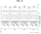
- FIG. 31 is a cross-sectional view taken along the line E4-E4' in FIG. 30
- FIG. 32 is a cross-sectional view taken along the line E5-E5' of FIG. 30 .
- the display device 10_4 may include the plurality of light transmitting layers TPL disposed in the area surrounded, in a plan view, by the upper bank layer UBN of each sub-pixel SPXn.
- the light transmitting layer TPL may be disposed on the light emitting elements ED.
- the light transmitting layer TPL may include a scatterer SCP and a base resin BRS and may emit light emitted from the light emitting element ED in an upward direction without conversion.
- the green light of the second color emitted by the second light emitting element ED2 may be emitted through the light transmitting layer TPL and the fifth color filter layer CFL5, and the green light of the second color may be emitted or displayed from the third light transmitting area TA3 of the third sub-pixel SPX3.
- the light transmitting layer TPL disposed in the fourth sub-pixel SPX4 is disposed to overlap a plurality of third light emitting elements ED3.
- the blue light of the third color emitted by the third light emitting element ED3 may be emitted through the light transmitting layer TPL and the sixth color filter layer CFL6, and the blue light of the third color may be emitted or displayed from the fourth light transmitting area TA4 of the fourth sub-pixel SPX4.
- the light transmitting layer TPL disposed in the second sub-pixel SPX2 may overlap the plurality of first light emitting elements ED1, second light emitting elements ED2, and third light emitting elements ED3. Further, the light transmitting layer TPL may also overlap the plurality of electrodes RME1, RME2, RME3, RME4, RME5, and RME6 spaced apart from each other. The light emitted from the first to third light emitting elements ED1, ED2, and ED3 may be emitted through the light transmitting layer TPL and the second to fourth color filter layers CFL2, CFL3, and CFL4, respectively. In the second light transmitting area TA2 of the second sub-pixel SPX2, the red light of the first color, the green light of the second color, and the blue light of the third color may be emitted simultaneously, or mixed light thereof may be emitted.
- the display device 10_4 may include the light emitting elements ED emitting lights of different colors in the sub-pixels SPXn with the light transmitting layer TPL disposed thereon.
- the display device 10_4 may include the first type sub-pixels (e.g., the first sub-pixel SPX1, the third sub-pixel SPX3, and the fourth sub-pixel SPX4) emitting any one of the light of the first color, the light of the second color, and the light of the third color, and the second type sub-pixel (e.g., the second sub-pixel SPX2) simultaneously emitting the light of the first color, the light of the second color, and the light of the third color or emitting mixed light thereof.
- the first type sub-pixels e.g., the first sub-pixel SPX1, the third sub-pixel SPX3, and the fourth sub-pixel SPX4
- the second type sub-pixel e.g., the second sub-pixel SPX2
- the bank layer BNL may be disposed to divide the second emission area EMA2 of the second sub-pixel SPX2 into a plurality of areas, and the upper bank layer UBN may be disposed to distinguish the plurality of sub light transmitting areas STA1, STA2, and STA3.
- different pairs of electrodes RME1, RME2, RME3, RME4, RME5, and RME6 may be disposed to correspond to the plurality of sub-emission areas SEA1, SEA2, and SEA3 distinguished by the bank layer BNL.
- Different first to third light emitting elements ED1, ED2, and ED3 and the connection electrodes CNE may also be disposed to correspond to the plurality of sub-emission areas SEA1, SEA2, and SEA3 distinguished by the bank layer BNL.
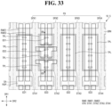
- the display device 10_5 may include the light emitting devices ED emitting different color light in the sub-pixels SPXn, and the structure of the bank layer BNL and the upper bank layer UBN may be the same as that in the embodiment shown in FIG. 20 .
- the display device 10_5 may be understood as an embodiment in which aspects of the embodiment shown in FIG. 20 and aspects of the embodiment shown in FIGS. 25 to 32 are combined. Description of the specific structure of the display device 10_5 is substantially the same as those in the above-described embodiments and a detailed description thereof will be omitted.
- FIG. 35 is a plan view illustrating a sub-pixel of a display device according to another embodiment
- FIG. 36 is a cross-sectional view taken along the line Q1-Q1' of FIG. 35
- FIG. 37 is a cross-sectional view taken along the line Q2-Q2' of FIG. 35 .
- the display device 10_6 may include a greater number of electrodes RME (e.g., RME1, RME2, RME3, and RME4), a greater number of barrier walls BP1, BP2, and BP3, a greater number of light emitting elements ED (e.g., ED1, ED2, ED3, and ED4), and a greater number of connection electrodes CNE (e.g., CNE1, CNE2, CNE3, CNE4, and CNE5).
- RME e.g., RME1, RME2, RME3, and RME4
- ED light emitting elements
- CNE connection electrodes
- the display device 10_6 is different from the embodiment shown in FIG. 9 in that a greater number of electrodes and a greater number of light emitting elements are included in each sub-pixel SPXn. In the following description, redundant description will be omitted and differences will be primarily described.
- the barrier walls BP1, BP2, and BP3 may further include a third barrier wall BP3 disposed between the first barrier wall BP1 and the second barrier wall BP2.
- the first barrier wall BP1 may be located on the left side in the drawings with respect to the center of the emission area EMA
- the second barrier wall BP2 may be located on the right side in the drawings with respect to the center of the emission area EMA
- the third barrier wall BP3 may be located at the center of the emission area EMA.
- the width of the third barrier wall BP3 measured in the second direction DR2 may be greater than those of the first barrier wall BP1 and the second barrier wall BP2 measured in the second direction DR2.
- the gap between the barrier walls BP1, BP2, and BP3 in the second direction DR2 may be greater than the gap between the electrodes RME.
- the first barrier wall BP1 may be disposed to partially overlap the first electrode RME1
- the second barrier wall BP2 may be disposed to partially overlap the fourth electrode RME4.
- the third barrier wall BP3 may be disposed to partially overlap the second electrode RME2 and the third electrode RME3. At least parts of the electrodes RME may be arranged without overlapping the barrier walls BP1, BP2, and BP3.
- the plurality of electrodes RME arranged for each sub-pixel SPXn may further include a third electrode RME3 and a fourth electrode RME4 in addition to a first electrode RME1 and a second electrode RME2.
- the first electrode RME1 and the second electrode RME2 may be in contact with the first conductive pattern CDP1 and the second voltage line VL2 disposed thereunder through the electrode contact holes CTD and CTS disposed under the bank layer BNL, respectively, and the third electrode RME3 and the fourth electrode RME4 may not be in contact with the first conductive pattern CDP1 and the second voltage line VL2.
- the first insulating layer PAS1 may be disposed in a structure similar to that in the above-described embodiments.
- the first insulating layer PAS1 may be disposed in the entire display area DPA and may cover the plurality of electrodes RME and the barrier walls BP1, BP2, and BP3.
- the plurality of light emitting elements ED may be arranged between the barrier walls BP1, BP2, and BP3 or on different electrodes RME. Some of the light emitting elements ED may be arranged between the first barrier wall BP1 and the third barrier wall BP3, and some other light emitting elements ED may be arranged between the third barrier wall BP3 and the second barrier wall BP2.
- the light emitting element ED may include a first light emitting element ED1 and a third light emitting element ED3 arranged between the first barrier wall BP1 and the third barrier wall BP3, and a second light emitting element ED2 and a fourth light emitting element ED4 arranged between the third barrier wall BP3 and the second barrier wall BP2.
- Each of the first light emitting element ED1 and the third light emitting element ED3 may be disposed above the first electrode RME1 and the third electrode RME3, and each of the second light emitting element ED2 and the fourth light emitting element ED4 may be disposed above the second electrode RME2 and the fourth electrode RME4.
- the first light emitting element ED1 and the second light emitting element ED2 may be arranged adjacent to the lower side of the emission area EMA of the corresponding sub-pixel SPXn in the drawings or adjacent to the sub-region SA, and the third light emitting element ED3 and the fourth light emitting element ED4 may be arranged adjacent to the upper side of the emission area EMA of the corresponding sub-pixel SPXn in the drawings.
- the light emitting elements ED may not be classified according to the arrangement position in the emission area EMA but may be classified according to a connection relationship with the connection electrode CNE, which will be described later. Both ends of each light emitting element ED may be in contact with different connection electrodes CNE according to an arrangement method of the connection electrodes CNE. The light emitting elements ED may be classified into different types of light emitting elements ED according to the type of the connection electrode CNE in contact therewith.
- the plurality of connection electrodes CNE may further include, in addition to the first connection electrode CNE1 disposed on the first electrode RME1, the second connection electrode CNE2 disposed on the second electrode RME2, a third connection electrode CNE3, a fourth connection electrode CNE4, and a fifth connection electrode CNE5 arranged across the plurality of electrodes RME.
- the third connection electrode CNE3 may include a first extension portion CN_E1 disposed on the third electrode RME3, a second extension portion CN_E2 disposed on the first electrode RME1, and a first connection portion CN_B1 that connects (e.g., extends between) the first extension portion CN_E1 to the second extension portion CN_E2.
- the first extension portion CN_E1 may be spaced apart from the first connection electrode CNE1 in the second direction DR2, and the second extension portion CN_E2 may be spaced apart from the first connection electrode CNE1 in the first direction DR1.
- the first extension portion CN_E1 may be disposed on the lower side of the emission area EMA of the corresponding sub-pixel SPXn in the drawings, and the second extension portion CN_E2 may be disposed on the upper side of the emission area EMA in the drawings.
- the first extension portion CN_E1 and the second extension portion CN_E2 may be disposed in the emission area EMA.
- the first connection portion CN_B1 may be disposed across the first electrode RME1 and the third electrode RME3 at the central portion of the emission area EMA.
- the third connection electrode CNE3 may have a shape substantially extending in the first direction DR1 and may have a shape that is bent in the second direction DR2 and extends again in the first direction DR1.
- the fourth connection electrode CNE4 may include a third extension portion CN_E3 disposed on the fourth electrode RME4, a fourth extension portion CN_E4 disposed on the second electrode RME2, and a second connection portion CN_B2 that connects (e.g., extends between) the third extension portion CN_E3 to the fourth extension portion CN_E4.
- the third extension portion CN_E3 may face and may be spaced apart from the second connection electrode CNE2 in the second direction DR2, and the fourth extension portion CN_E4 may be spaced apart from the second connection electrode CNE2 in the first direction DR1.
- the third extension portion CN_E3 may be disposed on the lower side of the emission area EMA of the corresponding sub-pixel SPXn in the drawings, and the fourth extension portion CN_E4 may be disposed on the upper side of the emission area EMA in the drawings.
- the third extension portion CN_E3 and the fourth extension portion CN_E4 may be disposed in the emission area EMA.
- the second connection portion CN_B2 may be disposed across the second electrode RME2 and the fourth electrode RME4 while being adjacent to the center of the emission area EMA.
- the fourth connection electrode CNE4 may have a shape substantially extending in the first direction DR1 and may have a shape that is bent in the second direction DR2 and extends again in the first direction DR1.
- the fifth connection electrode CNE5 may include a fifth extension portion CN_E5 disposed on the third electrode RME3, a sixth extension portion CN_E6 disposed on the fourth electrode RME4, and a third connection portion CN_B3 that connects the fifth extension portion CN_E5 to the sixth extension portion CN_E6.
- the fifth extension portion CN_E5 may face and may be spaced apart from the second extension portion CN_E2 of the third connection electrode CNE3 in the second direction DR2
- the sixth extension portion CN_E6 may face and may be spaced apart from the fourth extension portion CN_E4 of the fourth connection electrode CNE4 in the second direction DR2.
- Each of the fifth extension portion CN_E5 and the sixth extension portion CN_E6 may be arranged on the upper side of the emission area EMA, and the third connection portion CN_B3 may be disposed across the third electrode RME3, the second electrode RME2, and the fourth electrode RME4.
- the fifth connection electrode CNE5 may be disposed to surround, in a plan view, the fourth extension portion CN_E4 of the fourth connection electrode CNE4.
- the third connection electrode CNE3 may be in direct contact with the third electrode RME3 through the third contact portion CT3 penetrating the first insulating layer PAS1 and the second insulating layer PAS2 in the sub-region SA
- the fourth connection electrode CNE4 may be in direct contact with the fourth electrode RME4 through the fourth contact portion CT4 penetrating the first insulating layer PAS1 and the second insulating layer PAS2 in the sub-region SA.
- the first connection electrode CNE1 and the second connection electrode CNE2 may be the first type connection electrodes connected to the electrodes RME1 and RME2 directly connected to the third conductive layer, respectively.
- the third connection electrode CNE3 and the fourth connection electrode CNE4 may be the second type connection electrodes connected to the electrodes RME3 and RME4 that are not connected to the third conductive layer.
- the fifth connection electrode CNE5 may be the third type connection electrode that is not connected to the electrode RME.
- the fifth connection electrode CNE5 may be in contact with the light emitting elements ED without being connected to the electrode RME and may constitute an electrical connection circuit of the light emitting elements ED together with other connection electrodes CNE.
- the plurality of light emitting elements ED may be classified into different light emitting elements ED depending on the connection electrodes CNE in contact with both ends of the light emitting elements ED to correspond to the arrangement structure of the connection electrodes CNE.
- the first light emitting element ED1 and the second light emitting element ED2 may have first ends in contact with the first type connection electrodes and second ends in contact with the second type connection electrodes.
- the first light emitting element ED1 may be in contact with the first connection electrode CNE1 and the third connection electrode CNE3, and the second light emitting element ED2 may be in contact with the second connection electrode CNE2 and the fourth connection electrode CNE4.
- the plurality of light emitting elements ED may be connected in series through the plurality of connection electrodes CNE. Because the display device 10 according to this embodiment includes a greater number of light emitting elements ED for each sub-pixel SPXn and the light emitting elements ED are connected in series, the light emission amount per unit area may be further increased.
- first to sixth color filter layers CFL1, CFL2, CFL3, CFL4, CFL5, and CFL6 may be disposed to correspond to the color control structures TPL and WCL in each sub-pixel SPXn.
- This embodiment is different from the embodiment shown in FIGS. 9 to 14 in that four electrodes are arranged as one set and a greater number of light emitting elements ED are connected in series in each sub-pixel SPXn of the display device 10_6.
- the other descriptions are the same as those described above, and a detailed description thereof will be omitted.
Landscapes
- Electroluminescent Light Sources (AREA)
- Devices For Indicating Variable Information By Combining Individual Elements (AREA)
Applications Claiming Priority (1)
| Application Number | Priority Date | Filing Date | Title |
|---|---|---|---|
| KR1020220019009A KR20230123051A (ko) | 2022-02-14 | 2022-02-14 | 표시 장치 |
Publications (2)
| Publication Number | Publication Date |
|---|---|
| EP4239676A2 true EP4239676A2 (de) | 2023-09-06 |
| EP4239676A3 EP4239676A3 (de) | 2023-11-15 |
Family
ID=85251840
Family Applications (1)
| Application Number | Title | Priority Date | Filing Date |
|---|---|---|---|
| EP23156652.2A Pending EP4239676A3 (de) | 2022-02-14 | 2023-02-14 | Anzeigevorrichtung |
Country Status (4)
| Country | Link |
|---|---|
| US (1) | US20230261144A1 (de) |
| EP (1) | EP4239676A3 (de) |
| KR (1) | KR20230123051A (de) |
| CN (2) | CN116598407A (de) |
Family Cites Families (3)
| Publication number | Priority date | Publication date | Assignee | Title |
|---|---|---|---|---|
| KR20210142038A (ko) * | 2020-05-14 | 2021-11-24 | 삼성디스플레이 주식회사 | 표시 장치 및 표시 장치의 제조 방법 |
| KR102858557B1 (ko) * | 2020-07-24 | 2025-09-11 | 삼성디스플레이 주식회사 | 표시 장치 |
| KR102882321B1 (ko) * | 2020-07-28 | 2025-11-06 | 삼성디스플레이 주식회사 | 표시 장치 |
-
2022
- 2022-02-14 KR KR1020220019009A patent/KR20230123051A/ko active Pending
- 2022-12-07 US US18/063,036 patent/US20230261144A1/en active Pending
-
2023
- 2023-02-14 CN CN202310148519.3A patent/CN116598407A/zh active Pending
- 2023-02-14 CN CN202320216402.XU patent/CN219961262U/zh active Active
- 2023-02-14 EP EP23156652.2A patent/EP4239676A3/de active Pending
Also Published As
| Publication number | Publication date |
|---|---|
| KR20230123051A (ko) | 2023-08-23 |
| EP4239676A3 (de) | 2023-11-15 |
| CN219961262U (zh) | 2023-11-03 |
| CN116598407A (zh) | 2023-08-15 |
| US20230261144A1 (en) | 2023-08-17 |
Similar Documents
| Publication | Publication Date | Title |
|---|---|---|
| US12324313B2 (en) | Display device | |
| EP4120343A1 (de) | Anzeigevorrichtung | |
| CN221960993U (zh) | 显示装置 | |
| EP4496002A1 (de) | Anzeigevorrichtung | |
| KR20230017376A (ko) | 표시 장치 | |
| US12484355B2 (en) | Display device | |
| US12439761B2 (en) | Display device | |
| US12446381B2 (en) | Display device and method of fabricating the same | |
| US20220216264A1 (en) | Display device | |
| EP4239676A2 (de) | Anzeigevorrichtung | |
| KR20230118212A (ko) | 표시 장치 및 이의 제조 방법 | |
| CN223568012U (zh) | 显示设备 | |
| CN220210915U (zh) | 显示装置 | |
| EP4181221A1 (de) | Anzeigevorrichtung | |
| US20230275196A1 (en) | Display device | |
| EP4207278A1 (de) | Anzeigevorrichtung | |
| US12557451B2 (en) | Display device | |
| US12506130B2 (en) | Display device | |
| CN220358090U (zh) | 显示装置 | |
| US20230282785A1 (en) | Display device | |
| US20230317885A1 (en) | Display device | |
| US20230275189A1 (en) | Display device | |
| US20240014363A1 (en) | Display device | |
| US20230411371A1 (en) | Display device and method for manufacturing the same | |
| CN117637797A (zh) | 显示装置 |
Legal Events
| Date | Code | Title | Description |
|---|---|---|---|
| PUAI | Public reference made under article 153(3) epc to a published international application that has entered the european phase |
Free format text: ORIGINAL CODE: 0009012 |
|
| STAA | Information on the status of an ep patent application or granted ep patent |
Free format text: STATUS: THE APPLICATION HAS BEEN PUBLISHED |
|
| AK | Designated contracting states |
Kind code of ref document: A2 Designated state(s): AL AT BE BG CH CY CZ DE DK EE ES FI FR GB GR HR HU IE IS IT LI LT LU LV MC ME MK MT NL NO PL PT RO RS SE SI SK SM TR |
|
| PUAL | Search report despatched |
Free format text: ORIGINAL CODE: 0009013 |
|
| AK | Designated contracting states |
Kind code of ref document: A3 Designated state(s): AL AT BE BG CH CY CZ DE DK EE ES FI FR GB GR HR HU IE IS IT LI LT LU LV MC ME MK MT NL NO PL PT RO RS SE SI SK SM TR |
|
| RIC1 | Information provided on ipc code assigned before grant |
Ipc: H01L 33/50 20100101ALI20231011BHEP Ipc: H01L 25/075 20060101AFI20231011BHEP |
|
| STAA | Information on the status of an ep patent application or granted ep patent |
Free format text: STATUS: REQUEST FOR EXAMINATION WAS MADE |
|
| 17P | Request for examination filed |
Effective date: 20240318 |
|
| RBV | Designated contracting states (corrected) |
Designated state(s): AL AT BE BG CH CY CZ DE DK EE ES FI FR GB GR HR HU IE IS IT LI LT LU LV MC ME MK MT NL NO PL PT RO RS SE SI SK SM TR |
|
| P01 | Opt-out of the competence of the unified patent court (upc) registered |
Free format text: CASE NUMBER: UPC_APP_0006833_4239676/2026 Effective date: 20260226 |
|
| STAA | Information on the status of an ep patent application or granted ep patent |
Free format text: STATUS: EXAMINATION IS IN PROGRESS |