EP4239112A1 - Verfahren zur beurteilung der umgebung einer wärmebehandlung und siliciumcarbidsubstrat - Google Patents
Verfahren zur beurteilung der umgebung einer wärmebehandlung und siliciumcarbidsubstrat Download PDFInfo
- Publication number
- EP4239112A1 EP4239112A1 EP21886283.7A EP21886283A EP4239112A1 EP 4239112 A1 EP4239112 A1 EP 4239112A1 EP 21886283 A EP21886283 A EP 21886283A EP 4239112 A1 EP4239112 A1 EP 4239112A1
- Authority
- EP
- European Patent Office
- Prior art keywords
- heat treatment
- environment
- evaluating
- sic
- silicon carbide
- Prior art date
- Legal status (The legal status is an assumption and is not a legal conclusion. Google has not performed a legal analysis and makes no representation as to the accuracy of the status listed.)
- Pending
Links
Images




Classifications
-
- C—CHEMISTRY; METALLURGY
- C30—CRYSTAL GROWTH
- C30B—SINGLE-CRYSTAL GROWTH; UNIDIRECTIONAL SOLIDIFICATION OF EUTECTIC MATERIAL OR UNIDIRECTIONAL DEMIXING OF EUTECTOID MATERIAL; REFINING BY ZONE-MELTING OF MATERIAL; PRODUCTION OF A HOMOGENEOUS POLYCRYSTALLINE MATERIAL WITH DEFINED STRUCTURE; SINGLE CRYSTALS OR HOMOGENEOUS POLYCRYSTALLINE MATERIAL WITH DEFINED STRUCTURE; AFTER-TREATMENT OF SINGLE CRYSTALS OR A HOMOGENEOUS POLYCRYSTALLINE MATERIAL WITH DEFINED STRUCTURE; APPARATUS THEREFOR
- C30B29/00—Single crystals or homogeneous polycrystalline material with defined structure characterised by the material or by their shape
- C30B29/10—Inorganic compounds or compositions
- C30B29/36—Carbides
-
- G—PHYSICS
- G06—COMPUTING OR CALCULATING; COUNTING
- G06T—IMAGE DATA PROCESSING OR GENERATION, IN GENERAL
- G06T7/00—Image analysis
- G06T7/0002—Inspection of images, e.g. flaw detection
- G06T7/0004—Industrial image inspection
-
- C—CHEMISTRY; METALLURGY
- C30—CRYSTAL GROWTH
- C30B—SINGLE-CRYSTAL GROWTH; UNIDIRECTIONAL SOLIDIFICATION OF EUTECTIC MATERIAL OR UNIDIRECTIONAL DEMIXING OF EUTECTOID MATERIAL; REFINING BY ZONE-MELTING OF MATERIAL; PRODUCTION OF A HOMOGENEOUS POLYCRYSTALLINE MATERIAL WITH DEFINED STRUCTURE; SINGLE CRYSTALS OR HOMOGENEOUS POLYCRYSTALLINE MATERIAL WITH DEFINED STRUCTURE; AFTER-TREATMENT OF SINGLE CRYSTALS OR A HOMOGENEOUS POLYCRYSTALLINE MATERIAL WITH DEFINED STRUCTURE; APPARATUS THEREFOR
- C30B23/00—Single-crystal growth by condensing evaporated or sublimed materials
- C30B23/02—Epitaxial-layer growth
-
- C—CHEMISTRY; METALLURGY
- C30—CRYSTAL GROWTH
- C30B—SINGLE-CRYSTAL GROWTH; UNIDIRECTIONAL SOLIDIFICATION OF EUTECTIC MATERIAL OR UNIDIRECTIONAL DEMIXING OF EUTECTOID MATERIAL; REFINING BY ZONE-MELTING OF MATERIAL; PRODUCTION OF A HOMOGENEOUS POLYCRYSTALLINE MATERIAL WITH DEFINED STRUCTURE; SINGLE CRYSTALS OR HOMOGENEOUS POLYCRYSTALLINE MATERIAL WITH DEFINED STRUCTURE; AFTER-TREATMENT OF SINGLE CRYSTALS OR A HOMOGENEOUS POLYCRYSTALLINE MATERIAL WITH DEFINED STRUCTURE; APPARATUS THEREFOR
- C30B33/00—After-treatment of single crystals or homogeneous polycrystalline material with defined structure
- C30B33/02—Heat treatment
-
- C—CHEMISTRY; METALLURGY
- C30—CRYSTAL GROWTH
- C30B—SINGLE-CRYSTAL GROWTH; UNIDIRECTIONAL SOLIDIFICATION OF EUTECTIC MATERIAL OR UNIDIRECTIONAL DEMIXING OF EUTECTOID MATERIAL; REFINING BY ZONE-MELTING OF MATERIAL; PRODUCTION OF A HOMOGENEOUS POLYCRYSTALLINE MATERIAL WITH DEFINED STRUCTURE; SINGLE CRYSTALS OR HOMOGENEOUS POLYCRYSTALLINE MATERIAL WITH DEFINED STRUCTURE; AFTER-TREATMENT OF SINGLE CRYSTALS OR A HOMOGENEOUS POLYCRYSTALLINE MATERIAL WITH DEFINED STRUCTURE; APPARATUS THEREFOR
- C30B33/00—After-treatment of single crystals or homogeneous polycrystalline material with defined structure
- C30B33/08—Etching
- C30B33/12—Etching in gas atmosphere or plasma
-
- G—PHYSICS
- G01—MEASURING; TESTING
- G01N—INVESTIGATING OR ANALYSING MATERIALS BY DETERMINING THEIR CHEMICAL OR PHYSICAL PROPERTIES
- G01N23/00—Investigating or analysing materials by the use of wave or particle radiation, e.g. X-rays or neutrons, not covered by groups G01N3/00 – G01N17/00, G01N21/00 or G01N22/00
- G01N23/22—Investigating or analysing materials by the use of wave or particle radiation, e.g. X-rays or neutrons, not covered by groups G01N3/00 – G01N17/00, G01N21/00 or G01N22/00 by measuring secondary emission from the material
- G01N23/225—Investigating or analysing materials by the use of wave or particle radiation, e.g. X-rays or neutrons, not covered by groups G01N3/00 – G01N17/00, G01N21/00 or G01N22/00 by measuring secondary emission from the material using electron or ion
- G01N23/2251—Investigating or analysing materials by the use of wave or particle radiation, e.g. X-rays or neutrons, not covered by groups G01N3/00 – G01N17/00, G01N21/00 or G01N22/00 by measuring secondary emission from the material using electron or ion using incident electron beams, e.g. scanning electron microscopy [SEM]
-
- G—PHYSICS
- G01—MEASURING; TESTING
- G01N—INVESTIGATING OR ANALYSING MATERIALS BY DETERMINING THEIR CHEMICAL OR PHYSICAL PROPERTIES
- G01N33/00—Investigating or analysing materials by specific methods not covered by groups G01N1/00 - G01N31/00
- G01N33/0095—Semiconductive materials
-
- H—ELECTRICITY
- H10—SEMICONDUCTOR DEVICES; ELECTRIC SOLID-STATE DEVICES NOT OTHERWISE PROVIDED FOR
- H10P—GENERIC PROCESSES OR APPARATUS FOR THE MANUFACTURE OR TREATMENT OF DEVICES COVERED BY CLASS H10
- H10P14/00—Formation of materials, e.g. in the shape of layers or pillars
- H10P14/20—Formation of materials, e.g. in the shape of layers or pillars of semiconductor materials
- H10P14/29—Formation of materials, e.g. in the shape of layers or pillars of semiconductor materials characterised by the substrates
- H10P14/2901—Materials
- H10P14/2902—Materials being Group IVA materials
- H10P14/2904—Silicon carbide
-
- H—ELECTRICITY
- H10—SEMICONDUCTOR DEVICES; ELECTRIC SOLID-STATE DEVICES NOT OTHERWISE PROVIDED FOR
- H10P—GENERIC PROCESSES OR APPARATUS FOR THE MANUFACTURE OR TREATMENT OF DEVICES COVERED BY CLASS H10
- H10P14/00—Formation of materials, e.g. in the shape of layers or pillars
- H10P14/20—Formation of materials, e.g. in the shape of layers or pillars of semiconductor materials
- H10P14/29—Formation of materials, e.g. in the shape of layers or pillars of semiconductor materials characterised by the substrates
- H10P14/2926—Crystal orientations
-
- H—ELECTRICITY
- H10—SEMICONDUCTOR DEVICES; ELECTRIC SOLID-STATE DEVICES NOT OTHERWISE PROVIDED FOR
- H10P—GENERIC PROCESSES OR APPARATUS FOR THE MANUFACTURE OR TREATMENT OF DEVICES COVERED BY CLASS H10
- H10P50/00—Etching of wafers, substrates or parts of devices
-
- G—PHYSICS
- G01—MEASURING; TESTING
- G01N—INVESTIGATING OR ANALYSING MATERIALS BY DETERMINING THEIR CHEMICAL OR PHYSICAL PROPERTIES
- G01N23/00—Investigating or analysing materials by the use of wave or particle radiation, e.g. X-rays or neutrons, not covered by groups G01N3/00 – G01N17/00, G01N21/00 or G01N22/00
- G01N23/22—Investigating or analysing materials by the use of wave or particle radiation, e.g. X-rays or neutrons, not covered by groups G01N3/00 – G01N17/00, G01N21/00 or G01N22/00 by measuring secondary emission from the material
- G01N23/2202—Preparing specimens therefor
-
- G—PHYSICS
- G01—MEASURING; TESTING
- G01N—INVESTIGATING OR ANALYSING MATERIALS BY DETERMINING THEIR CHEMICAL OR PHYSICAL PROPERTIES
- G01N33/00—Investigating or analysing materials by specific methods not covered by groups G01N1/00 - G01N31/00
- G01N33/38—Concrete; Lime; Mortar; Gypsum; Bricks; Ceramics; Glass
- G01N33/388—Ceramics
-
- G—PHYSICS
- G06—COMPUTING OR CALCULATING; COUNTING
- G06T—IMAGE DATA PROCESSING OR GENERATION, IN GENERAL
- G06T2207/00—Indexing scheme for image analysis or image enhancement
- G06T2207/30—Subject of image; Context of image processing
- G06T2207/30108—Industrial image inspection
- G06T2207/30148—Semiconductor; IC; Wafer
-
- H—ELECTRICITY
- H10—SEMICONDUCTOR DEVICES; ELECTRIC SOLID-STATE DEVICES NOT OTHERWISE PROVIDED FOR
- H10P—GENERIC PROCESSES OR APPARATUS FOR THE MANUFACTURE OR TREATMENT OF DEVICES COVERED BY CLASS H10
- H10P74/00—Testing or measuring during manufacture or treatment of wafers, substrates or devices
- H10P74/20—Testing or measuring during manufacture or treatment of wafers, substrates or devices characterised by the properties tested or measured, e.g. structural or electrical properties
- H10P74/203—Structural properties, e.g. testing or measuring thicknesses, line widths, warpage, bond strengths or physical defects
-
- H—ELECTRICITY
- H10—SEMICONDUCTOR DEVICES; ELECTRIC SOLID-STATE DEVICES NOT OTHERWISE PROVIDED FOR
- H10P—GENERIC PROCESSES OR APPARATUS FOR THE MANUFACTURE OR TREATMENT OF DEVICES COVERED BY CLASS H10
- H10P90/00—Preparation of wafers not covered by a single main group of this subclass, e.g. wafer reinforcement
Definitions
- the present invention relates to a method for evaluating a heat treatment environment and relates to a silicon carbide substrate.
- SiC semiconductor devices have higher withstand voltage and are capable of operating at higher efficiency and higher temperature than silicon (Si) and gallium arsenide (GaAs) semiconductor devices. Therefore, the SiC semiconductor devices have been developed for industrialization.
- Patent Literature 1 a method for controlling a step-terrace structure of a SiC substrate has been proposed (see Patent Literature 1 and Patent Literature 2).
- Patent Literature 1 describes a technique of a method of manufacturing a SiC epitaxial wafer in which a surface pattern of a SiC substrate is controlled by using a C/Si concentration ratio of SiH 4 gas and C 3 H 8 gas simultaneously supplied to the SiC substrate.
- Patent Literature 2 describes a technique of a surface treatment method of a SiC substrate in which the SiC substrate is etched while an etching mode that is determined on the basis of at least a rate of etching, and a depth of etching are controlled, so that a surface pattern of the SiC substrate after etching is controlled.
- a step-terrace structure of a heat-treated SiC substrate is determined by an environment of heat treatment (hereinafter, referred to as a heat treatment environment.) experienced by the SiC substrate. Therefore, whether a desired step-terrace structure can be repeatedly reproduced depends on whether a desired heat treatment environment can be reproduced.
- the heat treatment environment has been indirectly evaluated by associating heat treatment conditions (a concentration ratio of source gas, a heating temperature, a growth rate, an etching rate, and the like) with the step-terrace structure (an AFM image and the like) obtained after the heat treatment (see Patent Literature 1 and Patent Literature 2.).
- an object of the present invention is to provide a novel technique for evaluating a heat treatment environment.
- the present invention is a method for evaluating a heat treatment environment, the method including:
- the notation "-" for Miller indices means a bar attached to an index immediately after the notation "-".
- the environment evaluation step is a step of evaluating the contrast information appearing on a terrace of the silicon carbide substrate.
- the environment evaluation step is a step of evaluating the contrast information appearing along a ⁇ 1-100> direction.
- the contrast information includes a plurality of pieces of brightness information reflecting a stacking direction of atoms
- the environment evaluation step includes a brightness comparison step of comparing the plurality of pieces of brightness information.
- the contrast information includes first brightness information reflecting the stacking direction of atoms and second brightness information capable of being compared with the first brightness information
- the environment evaluation step includes the brightness comparison step of comparing the first brightness information with the second brightness information
- the image acquisition step is a step of making the electron beam incident on the silicon carbide substrate, the electron beam being inclined to the ⁇ 1-100> direction.
- the environment evaluation step is a step of evaluating that the heat treatment environment is a Si-SiC equilibrium vapor pressure environment or a C-SiC equilibrium vapor pressure environment.
- the environment evaluation step is a step of evaluating that the heat treatment environment is a Si-rich environment or a C-rich environment.
- the silicon carbide substrate has a hexagonal crystal structure.
- a preferred mode of the present invention includes a heat treatment step of forming a step-terrace structure by heat-treating the silicon carbide substrate in the heat treatment environment.
- the silicon carbide substrate includes a step formation portion that serves as a generation source of a step during heat treatment, and an environment evaluation area where the step-terrace structure resulting from the step formation portion is formed, and the environment evaluation step is a step of evaluating the environment evaluation area.
- the step formation portion is a threading dislocation.
- the step formation portion is a machined hole.
- the environment evaluation area is a machined recess.
- the present invention also relates to a silicon carbide substrate. That is, to achieve the above-described object, the present invention is a silicon carbide substrate including: a step formation portion that serves as a generation source of a step during heat treatment; and an environment evaluation area where a step-terrace structure resulting from the step formation portion is formed.
- the step formation portion is a threading dislocation.
- the step formation portion is a machined hole.
- the environment evaluation area is a machined recess.
- Fig. 1 is an overview diagram illustrating steps of the method for evaluating a heat treatment environment according to an embodiment of the present invention.
- the method for evaluating a heat treatment environment according to the embodiment includes a heat treatment step S10 of forming a step-terrace structure by heat-treating a hexagonal SiC substrate 10 in a heat treatment environment HE, an image acquisition step S20 of acquiring an image I by making an electron beam PE incident at an incident angle ⁇ inclined with respect to a normal line N of a ⁇ 0001 ⁇ plane of the heat-treated SiC substrate 10, and an environment evaluation step S30 of evaluating the heat treatment environment HE of the SiC substrate 10 on the basis of contrast information C of the image I.
- the method for evaluating a heat treatment environment according to the present invention is characterized in that the heat treatment environment HE at the heat treatment step S10 is evaluated on the basis of the contrast information C of the image I acquired using the electron beam PE incident from a direction inclined with respect to the normal line N of the SiC substrate 10.
- the electron beam PE by acquiring the image I including a plurality of pieces of brightness information (the contrast information C) reflecting a stacking direction of atoms on a surface of the SiC substrate 10 by the electron beam PE, and comparing the plurality of pieces of brightness information appearing in the image I, it is possible to specify the heat treatment environment HE experienced by the SiC substrate 10.
- the heat treatment environment HE experienced by the SiC substrate 10 can be evaluated to be a Si-SiC equilibrium vapor pressure environment or a C-SiC equilibrium vapor pressure environment.
- the heat treatment environment HE experienced by the SiC substrate 10 can be evaluated to be a Si-rich environment or a C-rich environment.
- SiC-Si vapor pressure environment in the present specification refers to a vapor pressure environment when SiC (solid phase) and Si (liquid phase) are in a state of phase equilibrium via a gas phase.
- This SiC-Si equilibrium vapor pressure environment is formed, for example, by heat-treating a semi-closed space in which an atomic ratio Si/C exceeds 1.
- a SiC substrate satisfying a stoichiometric ratio 1 : 1 and a Si-vapor supply source are disposed in a SiC container satisfying a stoichiometric ratio 1 : 1, the atomic ratio Si/C in the container exceeds 1.
- the SiC-Si vapor pressure environment can be formed in the container.
- SiC-C equilibrium vapor pressure environment in the present specification refers to a vapor pressure environment when SiC (solid phase) and C (solid phase) are in a state of phase equilibrium via a gas phase.
- This SiC-C equilibrium vapor pressure environment is formed, for example, by heat-treating a semi-closed space in which an atomic ratio Si/C is equal to or less than 1.
- a SiC substrate satisfying a stoichiometric ratio 1 : 1 is disposed in a SiC container satisfying a stoichiometric ratio 1 : 1, the atomic ratio Si/C in the container becomes 1.
- a C-vapor supply source (a C pellet or the like) may be disposed to make the atomic ratio Si/C equal to or less than 1.
- the SiC-Si equilibrium vapor pressure environment and the SiC-C equilibrium vapor pressure environment in the present specification include a near-thermal equilibrium vapor pressure environment that satisfies a relationship between a growth rate and a growth temperature derived from a theoretical thermal equilibrium environment.
- the "semi-closed space” refers to a space in which the inside of the container can be evacuated while at least a part of vapor generated in the container can be confined.
- the semi-closed space can be formed in the container.
- the heat treatment environment HE experienced by the SiC substrate 10 can be evaluated by evaluating the SiC substrate 10 that has been heat-treated in advance. Therefore, the method for evaluating a heat treatment environment according to the present invention may include at least the image acquisition step S20 and the environment evaluation step S30.
- the heat treatment step S10 is a step of heat-treating the SiC substrate 10 in the heat treatment environment HE to be evaluated according to the present invention. Specifically, the heat treatment step S10 is a step of forming a step-terrace structure reflecting the heat treatment environment HE by heat-treating the hexagonal SiC substrate 10 in the heat treatment environment HE.
- a crystal growth method of forming a growth layer on the SiC substrate 10 and an etching method of etching the SiC substrate 10 can be given as examples of a method of the heat treatment step S10.
- crystal growth method examples include a chemical vapor deposition (CVD) method, a physical vapor transport (PVT) method, a metastable solvent epitaxy (MSE) method, and a confined physical vapor transport (CPVT) crystal growth method (see Fig. 2 ) to be described later.
- CVD chemical vapor deposition
- PVD physical vapor transport
- MSE metastable solvent epitaxy
- CPVT confined physical vapor transport
- etching method examples include a hydrogen etching method using hydrogen gas as etching gas, a Si-vapor etching (SiVE) method of performing heating under a Si atmosphere, and a CPVT etching method (see Fig. 3 ) to be described later.
- SiVE Si-vapor etching
- the heat treatment step S10 is a step of housing the SiC substrate 10 and a SiC material 20 inside a heat treatment container 30, and heating the heat treatment container 30 so as to form a temperature gradient inside the heat treatment container 30.
- the heat treatment container 30 is preferably housed in a refractory material container 40.
- the present embodiment may include a mode in which the SiC substrate 10 is crystal-grown and a mode in which the SiC substrate 10 is etched, according to a positional relationship between the SiC substrate 10 and the SiC material 20 and a direction of the temperature gradient.
- Fig. 2 is an explanatory view illustrating a mode in which the SiC substrate 10 is crystal-grown using the CPVT crystal growth method.
- the SiC substrate 10 and the SiC material 20 are disposed facing each other, and the heating is performed with such a temperature gradient that the SiC substrate 10 is on the low temperature side and the SiC material 20 is on the high temperature side.
- a Si element and a C element are transported from the SiC material 20 to the SiC substrate 10, so that a growth layer is grown on the SiC substrate 10.
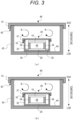
- Fig. 3 is an explanatory view illustrating a mode in which the SiC substrate 10 is etched using the CPVT etching method.
- the SiC substrate 10 and the SiC material 20 are disposed facing each other, and the heating is performed with such a temperature gradient that the SiC material 20 is on the low temperature side and the SiC substrate 10 is on the high temperature side.
- a Si element and a C element are transported from the SiC substrate 10 to the SiC material 20, so that the SiC substrate 10 is etched.
- Figs. 2 and 3 are in a relationship in which the positions of the SiC substrate 10 and the SiC material 20 are swapped.
- the transporting direction of the Si element and the C element may be reversed by reversing the direction of the temperature gradient without swapping the positions of the SiC substrate 10 and the SiC material 20.
- Figs. 2(a) and 3(a) illustrate a mode in which the SiC substrate 10 and the SiC material 20 are disposed and heat-treated in the semi-closed space in which the atomic ratio Si/C exceeds 1.
- the step-terrace structure corresponding to the Si-SiC equilibrium vapor pressure environment (the heat treatment environment HE) is formed on the surface of the SiC substrate 10.
- Figs. 2(b) and 3(b) illustrate a mode in which the SiC substrate 10 and the SiC material 20 are disposed and heat-treated in the semi-closed space in which the atomic ratio Si/C is equal to or less than 1.
- the step-terrace structure corresponding to the C-SiC equilibrium vapor pressure environment (the heat treatment environment HE) is formed on the surface of the SiC substrate 10.
- a substrate obtained by processing single-crystal SiC into a thin plate shape can be given as an example of the SiC substrate 10.
- a SiC wafer or the like obtained by slicing a SiC ingot produced by a sublimation method or the like into a disk shape can be given as an example.
- 200 or more kinds of polytypes of single-crystal SiC have been confirmed, and 4H-SiC and 6H-SiC are known as hexagonal polytypes having a high probability of occurrence and being important for application.
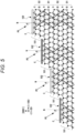
- Fig. 4 illustrates a schematic view of a 4H-SiC crystal structure.
- Fig. 4(a) is the 4H-SiC crystal structure viewed from a ⁇ 11-20> direction.
- Fig. 4(b) is the 4H-SiC crystal structure viewed from a [0001] direction.
- the notations "A, B, and C" in this drawing mean occupancy positions (corresponding to Si-C pairs) of three kinds of atoms in a hexagonal close-packed structure.
- Fig. 4(a) illustrating the 4H-SiC crystal structure the stacked atoms at the A and C positions correspond to a zinc-blende structure, and the stacked atoms at the B position correspond to a wurtzite structure.
- Fig. 5 illustrates a schematic view of the step-terrace structure formed on the surface of the SiC substrate 10.
- This step-terrace structure has a stair structure where a step 101, which is a level difference portion with one or more molecular layers, and a terrace 102, which is a flat portion where the ⁇ 0001 ⁇ plane is exposed, are alternately arranged.
- one molecular layer (0.25 nm) is a minimum height (minimum unit), and a plurality of the molecular layers are stacked to form various step heights.
- Fig. 5 illustrates the step 101 including the two molecular layers (0.5 nm: half-unit cell) of 4H-SiC.
- the SiC material 20 includes SiC capable of receiving or transferring the Si element and the C element from or to the SiC substrate 10 by being heated facing the SiC substrate 10.
- the SiC substrate 10 and the SiC material 20 as a substrate made of SiC face each other using a holder 34.
- a container made of SiC (the heat treatment container 30) or a container partly formed of SiC may be adopted as the SiC material 20.
- any polytype can be adopted, and polycrystal SiC may be adopted.
- the heat treatment container 30 can adopt any desired configuration if it is a configuration in which a vapor pressure of a gas-phase species containing the Si element and a gas-phase species containing the C element in an internal space is generated during the heat treatment. Examples of such a configuration include a configuration in which SiC is exposed on the inner side of the container, and a configuration in which the SiC material (the substrate made of SiC or the like) is separately disposed in the heat treatment container 30. In addition, a mode may be included in which a heat treatment container 30 including a material other than SiC is used to house a material that generates the Si element and the C element inside the container.
- the entire heat treatment container 30 includes polycrystal SiC.
- the environment in the heat treatment container 30 subjected to the heat treatment is a vapor pressure environment of a mixed system of the gas-phase species containing the Si element and the gas-phase species containing the C element.
- the gas-phase species containing the Si element include Si, Si 2 , Si 3 , Si 2 C, SiC 2 , and SiC.
- examples of the gas-phase species containing the C element include Si 2 C, SiC 2 , SiC, and C. That is, SiC-based gas is present in the heat treatment container 30.
- the heat treatment container 30 is a fitting container including an upper container 31 and a lower container 32 that can be fitted to each other.
- a minute gap 33 is formed in a fitting portion between the upper container 31 and the lower container 32, so that the inside of the heat treatment container 30 can be exhausted (evacuated) from the gap 33. That is, the inside of the heat treatment container 30 is the semi-closed space.
- the heat treatment container 30 may include the holder 34 that holds the SiC substrate 10 or the SiC material 20 in midair.
- the holder 34 only needs to be able to hold at least a part of the SiC substrate 10 in midair in the heat treatment container 30.
- any conventional support means such as a one-point support, a three-point support, a configuration for supporting an outer peripheral edge, and a configuration for clamping a part, can be reasonably adopted.
- a material of the holder 34 a refractory material can be adopted as a material of the holder 34.
- the holder 34 does not need to be provided depending on the form of the SiC material 20. That is, when the heat treatment container 30 itself is the SiC material 20, the SiC substrate 10 may be disposed on a bottom surface of the lower container 32 (without providing the holder 34).
- the heat treatment container 30 may include a Si-vapor supply source 35.
- the Si-vapor supply source 35 only needs to be configured to generate Si vapor in the heat treatment container 30 at the time of heating.
- Examples of the Si-vapor supply source 35 can include a solid of Si (a piece of single-crystal Si or a Si pellet of Si powder or the like) and a Si compound.
- the refractory material container 40 can adopt any desired configuration only if it is a configuration in which the heat treatment container 30 is accommodated and a vapor pressure (an atmosphere containing the Si element) of the gas-phase species containing the Si element in an internal space is generated during the heat treatment.
- the atmosphere containing the Si element in the inside of the refractory material container 40 according to the embodiment is formed using a Si-vapor supply source 44. Note that any desired method capable of forming the atmosphere containing the Si element around the heat treatment container 30 can be reasonably adopted.
- the refractory material container 40 includes a refractory material.
- the refractory material include C, which is a general-purpose heat resistant member, W, Re, Os, Ta, and Mo, which are refractory metals, Ta 9 C 8 , HfC, TaC, NbC, ZrC, Ta 2 C, TiC, WC, and MoC, which are carbides, HfN, TaN, BN, Ta 2 N, ZrN, and TiN, which are nitrides, and HfB 2 , TaB 2 , ZrB 2 , NB 2 , TiB 2 , and polycrystal SiC, which are borides.
- the refractory material container 40 is a fitting container including an upper container 41 and a lower container 42 that can be fitted to each other, and is capable of accommodating the heat treatment container 30.
- a minute gap 43 is formed in a fitting portion between the upper container 41 and the lower container 42, so that the inside of the refractory material container 40 can be exhausted (evacuated) from the gap 43.
- the refractory material container 40 preferably includes the Si-vapor supply source 44 capable of supplying the vapor pressure of the gas-phase species containing the Si element to the inside of the refractory material container 40.
- the Si-vapor supply source 44 only needs to be configured to generate Si vapor in the inside of the refractory material container 40 at the time of heating.
- Examples of the Si-vapor supply source 44 include a solid of Si (a piece of single-crystal Si or a Si pellet of Si powder or the like) and a Si compound.
- TaC is used as the material of the refractory material container 40
- tantalum silicide is used as the Si-vapor supply source 44.
- a tantalum silicide layer is formed on the inner side of the refractory material container 40. The Si vapor is supplied from the tantalum silicide layer into the container at the time of heating, whereby the Si vapor pressure environment is formed.
- the image acquisition step S20 is a step of acquiring the image I including the contrast information C of the terrace 102 reflecting the stacking direction of the atoms on the surface of the SiC substrate 10 by making the electron beam PE incident on the SiC substrate 10 at the incident angle ⁇ inclined with respect to the normal line N of the ⁇ 0001 ⁇ plane of the SiC substrate 10.
- the image acquisition step S20 includes an installation step S21 of installing the SiC substrate 10 on a stage of a scanning electron microscope, an inclination step S22 of inclining the stage such that the electron beam PE is incident on the SiC substrate 10 at the incident angle ⁇ inclined with respect to the normal line N of the ⁇ 0001 ⁇ plane of the SiC substrate 10, and an electron beam irradiation step S23 of irradiating the SiC substrate 10 with the electron beam PE to obtain the image I.
- the stage is preferably inclined such that the electron beam PE is inclined to a ⁇ 1-100> direction with respect to the normal line N of the SiC substrate 10.
- An inclination angle ⁇ of the stage at the inclination step S22 is inclined so that the incident angle ⁇ of the electron beam PE is preferably in a range between 22° and 42° inclusive, more preferably in a range between 27° and 37° inclusive, and still more preferably in a range between 30° and 31° inclusive.
- the inclination angle ⁇ of the stage at the inclination step S22 is inclined so that the incident angle ⁇ of the electron beam PE is preferably in a range between 5° and 10° inclusive, more preferably in a range between 7° and 9° inclusive, and still more preferably 8°.
- the irradiation with the electron beam PE is preferably performed at an acceleration voltage of 1.0 kV or less.
- the image I is created on the basis of electrons (reflected electrons) obtained when the electron beam PE (primary electrons) emitted by an electron emission unit of the scanning electron microscope is bounced back on the surface of the SiC substrate 10, or emitted after the electron beam PE interacts with the SiC substrate 10, and electrons (secondary electrons) generated during the interaction.
- a detector disposed in the scanning electron microscope detects the reflected electrons and/or the secondary electrons, and the image I is created on the basis of positional information of the SiC substrate 10 and the detection results of the respective electrons.
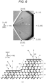
- Fig. 6 is an explanatory view illustrating the image I obtained at the image acquisition step S20 for the SiC substrate 10 heat-treated in the Si-SiC equilibrium vapor pressure environment (the heat treatment environment HE) at the heat treatment step S10.
- Fig. 6(a) is the image I of the SiC substrate 10 heat-treated in the Si-SiC equilibrium vapor pressure environment.
- Fig. 6(b) is a schematic view of the crystal structure of the SiC substrate 10 heat-treated in the Si-SiC equilibrium vapor pressure environment.
- Fig. 7 is an explanatory view illustrating the image I obtained at the image acquisition step S20 for the SiC substrate 10 heat-treated in the C-SiC equilibrium vapor pressure environment (the heat treatment environment HE) at the heat treatment step S10.
- Fig. 7(a) is the image I of the SiC substrate 10 heat-treated in the C-SiC equilibrium vapor pressure environment.
- Fig. 7(b) is a schematic view of the crystal structure of the SiC substrate 10 heat-treated in the C-SiC equilibrium vapor pressure environment.
- the environment evaluation step S30 is a step of evaluating the heat treatment environment HE of the SiC substrate 10 on the basis of the contrast information C of the image I.
- the environment evaluation step S30 is a step of evaluating the contrast information C appearing on the terrace 102 of the SiC substrate 10.
- the environment evaluation step S30 is a step of evaluating the contrast information C appearing along the ⁇ 1-100> direction.
- the contrast information C includes the plurality of pieces of brightness information reflecting the stacking direction of the atoms on the surface of the SiC substrate 10. Specifically, the contrast information C includes first brightness information C1 appearing along the ⁇ 1-100> direction and second brightness information C2 capable of being compared with the first brightness information C1.
- the environment evaluation step S30 includes a brightness comparison step S31 of comparing the plurality of pieces of brightness information, and a crystal structure specification step S32 of specifying the crystal structure of the outermost surface (the terrace 102) of the SiC substrate 10 on the basis of the plurality of pieces of brightness information.
- the brightness comparison step S31 is a step of comparing the plurality of pieces of brightness information. Specifically, the brightness comparison step S31 is a step of evaluating whether the first brightness information C1 appearing along the ⁇ 1-100> direction is white or black by comparing the brightness of the first brightness information C1 with the brightness of the second brightness information C2. That is, the plurality of pieces of brightness information are compared to evaluate whether the area of the terrace 102 used for evaluation is relatively black or white at this step.
- the crystal structure specification step S32 is a step of obtaining information regarding the crystal structure of the outermost surface (the terrace 102) of the SiC substrate 10 from a relationship between the first brightness information C1 obtained at the brightness comparison step S31 and the inclination direction of the incident angle ⁇ of the electron beam PE (the incident direction of the electron beam PE) with respect to the SiC substrate 10.
- the black contrast information C is obtained.
- the white contrast information C is obtained.
- the stacking direction of the atoms of the terrace 102 is the first stacking direction D1 or the second stacking direction D2.
- Fig. 6 is the image I acquired by irradiating the SiC substrate 10 heat-treated in the Si-SiC equilibrium vapor pressure environment, with the electron beam PE from a [-1100] direction (a left-side direction in Fig. 6 ).
- the first brightness information C1 appearing on the terrace 102 in a [1-100] direction of the image I is black by comparison with the second brightness information C2 (the brightness comparison step S31).
- the second brightness information C2 compared with the first brightness information C1 appears to be white in an area between a [10-10] direction and a [2-1-10] direction, for example.
- the stacking direction of the atoms of the terrace 102 in the [1-100] direction can be evaluated to be the first stacking direction D1.
- the terrace 102 of the SiC substrate 10 heat-treated in the Si-SiC equilibrium vapor pressure environment can be evaluated to form a surface where a C element having two dangling bonds is present at the end of the step 101 in the ⁇ 1-100> direction.
- the heat treatment environment experienced by the SiC substrate 10 can be evaluated to be the Si-SiC equilibrium vapor pressure environment.
- the contrast information C is reversed. That is, the first brightness information C1 reflecting the crystal structure in the first stacking direction D1 is white, and the second brightness information C2 reflecting the crystal structure in the second stacking direction D2 is black.
- the contrast information C (the first brightness information C1 and the second brightness information C2) is determined by the relationship between the irradiation direction of the electron beam PE and the stacking direction of the SiC substrate 10. Therefore, at the crystal structure specification step S32, it is necessary to evaluate the stacking direction of the area of the first brightness information C1 from the crystal structure of the SiC substrate 10 and the direction irradiated with the electron beam PE.
- Fig. 7 is the image I acquired by irradiating the SiC substrate 10 heat-treated in the C-SiC equilibrium vapor pressure environment, with the electron beam PE from the [-1100] direction (the left-side direction in the drawing).
- the first brightness information C1 appearing on the terrace 102 in the [1-100] direction of the image I is white by comparison with the second brightness information C2 (the brightness comparison step S31).
- the second brightness information C2 compared with the first brightness information C1 appears to be black in the area between the [10-10] direction and the [2-1-10] direction, for example.
- the stacking direction of the atoms of the terrace 102 in the [1-100] direction can be evaluated to be the second stacking direction D2.
- the terrace 102 of the SiC substrate 10 heat-treated in the C-SiC equilibrium vapor pressure environment can be evaluated to form a surface where a C element having one dangling bond is present at the end of the step 101 in the ⁇ 1-100> direction.
- the heat treatment environment experienced by the SiC substrate 10 can be evaluated to be the C-SiC equilibrium vapor pressure environment.
- the first brightness information C1 is black and the second brightness information C2 is white.
- the method for evaluating a heat treatment environment includes: the image acquisition step S20 of acquiring the image I by making the electron beam PE incident at the incident angle ⁇ inclined with respect to the normal line N of the ⁇ 0001 ⁇ plane of the heat-treated SiC substrate 10; and the environment evaluation step S30 of evaluating the heat treatment environment HE of the SiC substrate 10 on the basis of the contrast information C of the image I.
- the stacking direction of the atoms of the terrace 102 reflecting the heat treatment environment HE is evaluated. Therefore, the heat treatment environment HE can be evaluated without being locally affected by crystal defects, a subsurface damaged layer, and the like of the SiC substrate 10.
- the method for evaluating a heat treatment environment it is possible to evaluate the heat treatment environment HE easily only by acquiring the image I of the SiC substrate 10 using the scanning electron microscope. That is, as illustrated in Figs. 6 and 7 , whether the heat treatment environment HE is the Si-SiC equilibrium vapor pressure environment or the C-SiC equilibrium vapor pressure environment can be evaluated on the basis of the contrast information C of the image I.
- a SiC substrate 50 has an evaluation pattern 60 for evaluating the heat treatment environment HE.
- the evaluation pattern 60 includes a step formation portion 61 that serves as a generation source of the step 101 during the heat treatment, and an environment evaluation area 62 where the step-terrace structure resulting from the step formation portion 61 is formed.
- Fig. 8 illustrates an example in which a plurality of the evaluation patterns 60 are formed on a SiC wafer. By interspersing the SiC wafer with the evaluation patterns 60 as described above, it is possible to evaluate the heat treatment environment HE at each location.
- the size and shape of the SiC substrate 50 and the number of evaluation patterns 60 are not limited.
- an individual piece where one evaluation pattern 60 is formed may be adopted as an evaluation sample of the heat treatment environment HE.
- Fig. 9 is an example of the evaluation pattern 60, which includes a machined hole 611 serving as the step formation portion 61 and a machined recess 621 serving as the environment evaluation area 62.
- a cliff portion 63 is formed between the machined hole 611 and the machined recess 621.
- etching preferentially proceeds from the cliff portion 63. Therefore, the terrace 102 reflecting the heat treatment environment HE is formed in an area inside the machined recess 621.
- Fig. 10 is an example of the evaluation pattern 60, which includes a threading dislocation 612 serving as the step formation portion 61 and a machined recess 622 serving as the environment evaluation area 62.
- a threading edge dislocation or a threading screw dislocation as the threading dislocation 612 is preferentially grown or etched when the heat treatment is performed in the heat treatment environment HE. Therefore, the terrace 102 reflecting the heat treatment environment HE is formed in an area inside the machined recess 622.
- the SiC substrate 50 according to the present invention includes the step formation portion 61 that serves as the generation source of the step 101 during the heat treatment, and the environment evaluation area 62 where the step-terrace structure resulting from the step formation portion 61 is formed.
Landscapes
- Engineering & Computer Science (AREA)
- Chemical & Material Sciences (AREA)
- Physics & Mathematics (AREA)
- General Physics & Mathematics (AREA)
- Crystallography & Structural Chemistry (AREA)
- Materials Engineering (AREA)
- Metallurgy (AREA)
- Organic Chemistry (AREA)
- Health & Medical Sciences (AREA)
- Life Sciences & Earth Sciences (AREA)
- Theoretical Computer Science (AREA)
- Computer Vision & Pattern Recognition (AREA)
- Quality & Reliability (AREA)
- Analytical Chemistry (AREA)
- Biochemistry (AREA)
- General Health & Medical Sciences (AREA)
- Immunology (AREA)
- Pathology (AREA)
- Plasma & Fusion (AREA)
- Thermal Sciences (AREA)
- Food Science & Technology (AREA)
- Medicinal Chemistry (AREA)
- Inorganic Chemistry (AREA)
- Crystals, And After-Treatments Of Crystals (AREA)
- Testing Or Measuring Of Semiconductors Or The Like (AREA)
- Analysing Materials By The Use Of Radiation (AREA)
Applications Claiming Priority (2)
| Application Number | Priority Date | Filing Date | Title |
|---|---|---|---|
| JP2020180971 | 2020-10-28 | ||
| PCT/JP2021/039699 WO2022092166A1 (ja) | 2020-10-28 | 2021-10-27 | 熱処理環境の評価方法及び炭化ケイ素基板 |
Publications (2)
| Publication Number | Publication Date |
|---|---|
| EP4239112A1 true EP4239112A1 (de) | 2023-09-06 |
| EP4239112A4 EP4239112A4 (de) | 2024-07-17 |
Family
ID=81381489
Family Applications (1)
| Application Number | Title | Priority Date | Filing Date |
|---|---|---|---|
| EP21886283.7A Pending EP4239112A4 (de) | 2020-10-28 | 2021-10-27 | Verfahren zur beurteilung der umgebung einer wärmebehandlung und siliciumcarbidsubstrat |
Country Status (6)
| Country | Link |
|---|---|
| US (1) | US20240020814A1 (de) |
| EP (1) | EP4239112A4 (de) |
| JP (1) | JP7849581B2 (de) |
| CN (1) | CN116348640A (de) |
| TW (1) | TWI912396B (de) |
| WO (1) | WO2022092166A1 (de) |
Families Citing this family (1)
| Publication number | Priority date | Publication date | Assignee | Title |
|---|---|---|---|---|
| CN119086627B (zh) * | 2024-11-08 | 2025-02-18 | 中国石油大学(华东) | 一种不同地层环境页岩原位转化烃物质相态参数测定系统 |
Family Cites Families (9)
| Publication number | Priority date | Publication date | Assignee | Title |
|---|---|---|---|---|
| JP4959763B2 (ja) | 2009-08-28 | 2012-06-27 | 昭和電工株式会社 | SiCエピタキシャルウェハ及びその製造方法 |
| JP6268277B2 (ja) * | 2014-03-31 | 2018-01-24 | 東洋炭素株式会社 | SiC基板の表面処理方法、SiC基板の製造方法、及び半導体の製造方法 |
| US9810150B2 (en) | 2014-10-21 | 2017-11-07 | United Technologies Corporation | Heat exchanger assembly |
| CN107002288B (zh) * | 2014-11-18 | 2020-10-16 | 学校法人关西学院 | 碳化硅基板的表面处理方法 |
| JP6664133B2 (ja) * | 2016-04-27 | 2020-03-13 | 学校法人関西学院 | 傾斜支持台付き標準試料、その製造方法、走査型電子顕微鏡の評価方法、及びSiC基板の評価方法 |
| JP6708875B2 (ja) | 2016-04-27 | 2020-06-10 | 学校法人関西学院 | グラフェン前駆体付きSiC基板の製造方法及びSiC基板の表面処理方法 |
| US11107655B2 (en) * | 2017-09-20 | 2021-08-31 | Hitachi High-Technologies Corporation | Charged particle beam device |
| CN113227466A (zh) * | 2018-11-05 | 2021-08-06 | 学校法人关西学院 | SiC半导体衬底及其制造方法和制造装置 |
| TWI875720B (zh) * | 2018-11-05 | 2025-03-11 | 學校法人關西學院 | 碳化矽半導體基板、碳化矽半導體基板的製造方法以及降低碳化矽半導體基板之底面差排的方法 |
-
2021
- 2021-10-27 JP JP2022559209A patent/JP7849581B2/ja active Active
- 2021-10-27 US US18/250,710 patent/US20240020814A1/en active Pending
- 2021-10-27 WO PCT/JP2021/039699 patent/WO2022092166A1/ja not_active Ceased
- 2021-10-27 TW TW110139783A patent/TWI912396B/zh active
- 2021-10-27 EP EP21886283.7A patent/EP4239112A4/de active Pending
- 2021-10-27 CN CN202180070316.6A patent/CN116348640A/zh active Pending
Also Published As
| Publication number | Publication date |
|---|---|
| EP4239112A4 (de) | 2024-07-17 |
| TW202233913A (zh) | 2022-09-01 |
| JP7849581B2 (ja) | 2026-04-22 |
| JPWO2022092166A1 (de) | 2022-05-05 |
| CN116348640A (zh) | 2023-06-27 |
| US20240020814A1 (en) | 2024-01-18 |
| TWI912396B (zh) | 2026-01-21 |
| WO2022092166A1 (ja) | 2022-05-05 |
Similar Documents
| Publication | Publication Date | Title |
|---|---|---|
| EP1721031B1 (de) | Verringerung von karottendefekten bei der siliciumcarbid-epitaxie | |
| EP2059946B1 (de) | Mikroröhrchen-freies siliciumcarbid und verfahren zu seiner herstellung | |
| TWI875794B (zh) | 碳化矽基板及其製造方法、碳化矽磊晶基板及其製造方法以及碳化矽鑄錠及其製造方法 | |
| US12209328B2 (en) | Method of manufacturing semiconductor substrate and epitaxial growth method | |
| Hemmingsson et al. | Optimization of low temperature GaN buffer layers for halide vapor phase epitaxy growth of bulk GaN | |
| US12534825B2 (en) | SiC epitaxial substrate manufacturing method and manufacturing device therefor | |
| Katona et al. | Observation of crystallographic wing tilt in cantilever epitaxy of GaN on silicon carbide and silicon (111) substrates | |
| EP4239112A1 (de) | Verfahren zur beurteilung der umgebung einer wärmebehandlung und siliciumcarbidsubstrat | |
| EP1249521A1 (de) | Sic-einkristall und herstellungsverfahren dafür | |
| US11952678B2 (en) | Method for manufacturing etched SiC substrate and grown SiC substrate by material tranportation and method for epitaxial growth by material transportation | |
| JP2006052097A (ja) | 炭化珪素単結晶育成用種結晶と炭化珪素単結晶インゴット及びその製造方法 | |
| US12509795B2 (en) | Method for manufacturing aluminum nitride substrate, aluminum nitride substrate, and method for forming aluminum nitride layer | |
| Wissel-Garcia et al. | Growth regimes of (0001) AlN by ammonia molecular beam epitaxy | |
| EP4036285A1 (de) | Verfahren zur herstellung von halbleitersubstraten und vorrichtung zur herstellung von halbleitersubstraten | |
| EP4137616A1 (de) | Verfahren zur herstellung eines aluminiumnitridsubstrats, aluminiumnitridsubstrat und verfahren zur unterdrückung der einführung einer versetzung in eine aluminiumnitrid-wachstumsschicht | |
| EP4571821A1 (de) | Verfahren zur unterdrückung der änderung der lichtemissionsintensität des hintergrunds bei der photolumineszenzmessung und beurteilungsverfahren für ein halbleitersubstrat | |
| US12460315B2 (en) | Method for manufacturing semiconductor substrates and method for suppressing introduction of displacement to growth layer | |
| US20250051962A1 (en) | Method for reducing stacking faults in silicon carbide, and structure created by means of said method | |
| Lu | Sublimation growth of aluminum nitride bulk crystals and high-speed CVD growth of silicon carbide epilayers, and their characterization | |
| JP6457442B2 (ja) | GaN結晶基板 | |
| Devrajan | Growth of SiC thin films on SOI substrates by RTCVD | |
| Tempez | Chemical beam epitaxy of gallium nitride on silicon: Use of silicon carbide as template and selective area growth | |
| Teker | Research on the epitaxial growth of silicon carbide on silicon and aluminum nitride | |
| Thomas | MOCVD optimization and characterization of AlN for the development of an AlN/SiC {p/pn} heterojunction UV detector | |
| Klein | Optimizing Structured SiN-masks for Self Separation of Full 2”-GaN Wafers by Hydride Vapor Phase Epitaxy |
Legal Events
| Date | Code | Title | Description |
|---|---|---|---|
| STAA | Information on the status of an ep patent application or granted ep patent |
Free format text: STATUS: THE INTERNATIONAL PUBLICATION HAS BEEN MADE |
|
| PUAI | Public reference made under article 153(3) epc to a published international application that has entered the european phase |
Free format text: ORIGINAL CODE: 0009012 |
|
| STAA | Information on the status of an ep patent application or granted ep patent |
Free format text: STATUS: REQUEST FOR EXAMINATION WAS MADE |
|
| 17P | Request for examination filed |
Effective date: 20230329 |
|
| AK | Designated contracting states |
Kind code of ref document: A1 Designated state(s): AL AT BE BG CH CY CZ DE DK EE ES FI FR GB GR HR HU IE IS IT LI LT LU LV MC MK MT NL NO PL PT RO RS SE SI SK SM TR |
|
| DAV | Request for validation of the european patent (deleted) | ||
| DAX | Request for extension of the european patent (deleted) | ||
| REG | Reference to a national code |
Ref country code: DE Ref legal event code: R079 Free format text: PREVIOUS MAIN CLASS: C30B0029360000 Ipc: C30B0023020000 |
|
| A4 | Supplementary search report drawn up and despatched |
Effective date: 20240617 |
|
| RIC1 | Information provided on ipc code assigned before grant |
Ipc: H01L 21/66 20060101ALN20240611BHEP Ipc: H01L 21/02 20060101ALN20240611BHEP Ipc: G01N 33/38 20060101ALN20240611BHEP Ipc: G01N 23/2202 20180101ALN20240611BHEP Ipc: G06T 7/00 20170101ALI20240611BHEP Ipc: G01N 33/00 20060101ALI20240611BHEP Ipc: G01N 23/2251 20180101ALI20240611BHEP Ipc: C30B 33/12 20060101ALI20240611BHEP Ipc: C30B 33/02 20060101ALI20240611BHEP Ipc: C30B 29/36 20060101ALI20240611BHEP Ipc: C30B 23/02 20060101AFI20240611BHEP |