EP4231613A2 - Faltbare anzeigevorrichtung - Google Patents
Faltbare anzeigevorrichtung Download PDFInfo
- Publication number
- EP4231613A2 EP4231613A2 EP23185403.5A EP23185403A EP4231613A2 EP 4231613 A2 EP4231613 A2 EP 4231613A2 EP 23185403 A EP23185403 A EP 23185403A EP 4231613 A2 EP4231613 A2 EP 4231613A2
- Authority
- EP
- European Patent Office
- Prior art keywords
- layer
- digitizer
- disposed
- display
- display apparatus
- Prior art date
- Legal status (The legal status is an assumption and is not a legal conclusion. Google has not performed a legal analysis and makes no representation as to the accuracy of the status listed.)
- Granted
Links
Images


Classifications
-
- G—PHYSICS
- G06—COMPUTING OR CALCULATING; COUNTING
- G06F—ELECTRIC DIGITAL DATA PROCESSING
- G06F1/00—Details not covered by groups G06F3/00 - G06F13/00 and G06F21/00
- G06F1/16—Constructional details or arrangements
- G06F1/1613—Constructional details or arrangements for portable computers
- G06F1/1615—Constructional details or arrangements for portable computers with several enclosures having relative motions, each enclosure supporting at least one I/O or computing function
- G06F1/1616—Constructional details or arrangements for portable computers with several enclosures having relative motions, each enclosure supporting at least one I/O or computing function with folding flat displays, e.g. laptop computers or notebooks having a clamshell configuration, with body parts pivoting to an open position around an axis parallel to the plane they define in closed position
-
- H—ELECTRICITY
- H04—ELECTRIC COMMUNICATION TECHNIQUE
- H04M—TELEPHONIC COMMUNICATION
- H04M1/00—Substation equipment, e.g. for use by subscribers
- H04M1/02—Constructional features of telephone sets
- H04M1/0202—Portable telephone sets, e.g. cordless phones, mobile phones or bar type handsets
- H04M1/0206—Portable telephones comprising a plurality of mechanically joined movable body parts, e.g. hinged housings
- H04M1/0208—Portable telephones comprising a plurality of mechanically joined movable body parts, e.g. hinged housings characterized by the relative motions of the body parts
- H04M1/0214—Foldable telephones, i.e. with body parts pivoting to an open position around an axis parallel to the plane they define in closed position
- H04M1/0216—Foldable in one direction, i.e. using a one degree of freedom hinge
-
- G—PHYSICS
- G09—EDUCATION; CRYPTOGRAPHY; DISPLAY; ADVERTISING; SEALS
- G09F—DISPLAYING; ADVERTISING; SIGNS; LABELS OR NAME-PLATES; SEALS
- G09F9/00—Indicating arrangements for variable information in which the information is built-up on a support by selection or combination of individual elements
- G09F9/30—Indicating arrangements for variable information in which the information is built-up on a support by selection or combination of individual elements in which the desired character or characters are formed by combining individual elements
- G09F9/301—Indicating arrangements for variable information in which the information is built-up on a support by selection or combination of individual elements in which the desired character or characters are formed by combining individual elements flexible foldable or roll-able electronic displays, e.g. thin LCD, OLED
-
- G—PHYSICS
- G06—COMPUTING OR CALCULATING; COUNTING
- G06F—ELECTRIC DIGITAL DATA PROCESSING
- G06F1/00—Details not covered by groups G06F3/00 - G06F13/00 and G06F21/00
- G06F1/16—Constructional details or arrangements
- G06F1/1613—Constructional details or arrangements for portable computers
- G06F1/1633—Constructional details or arrangements of portable computers not specific to the type of enclosures covered by groups G06F1/1615 - G06F1/1626
- G06F1/1637—Details related to the display arrangement, including those related to the mounting of the display in the housing
- G06F1/1643—Details related to the display arrangement, including those related to the mounting of the display in the housing the display being associated to a digitizer, e.g. laptops that can be used as penpads
-
- G—PHYSICS
- G06—COMPUTING OR CALCULATING; COUNTING
- G06F—ELECTRIC DIGITAL DATA PROCESSING
- G06F1/00—Details not covered by groups G06F3/00 - G06F13/00 and G06F21/00
- G06F1/16—Constructional details or arrangements
- G06F1/1613—Constructional details or arrangements for portable computers
- G06F1/1633—Constructional details or arrangements of portable computers not specific to the type of enclosures covered by groups G06F1/1615 - G06F1/1626
- G06F1/1637—Details related to the display arrangement, including those related to the mounting of the display in the housing
- G06F1/1652—Details related to the display arrangement, including those related to the mounting of the display in the housing the display being flexible, e.g. mimicking a sheet of paper, or rollable
-
- G—PHYSICS
- G06—COMPUTING OR CALCULATING; COUNTING
- G06F—ELECTRIC DIGITAL DATA PROCESSING
- G06F1/00—Details not covered by groups G06F3/00 - G06F13/00 and G06F21/00
- G06F1/16—Constructional details or arrangements
- G06F1/1613—Constructional details or arrangements for portable computers
- G06F1/1633—Constructional details or arrangements of portable computers not specific to the type of enclosures covered by groups G06F1/1615 - G06F1/1626
- G06F1/1656—Details related to functional adaptations of the enclosure, e.g. to provide protection against EMI, shock, water, or to host detachable peripherals like a mouse or removable expansions units like PCMCIA cards, or to provide access to internal components for maintenance or to removable storage supports like CDs or DVDs, or to mechanically mount accessories
-
- G—PHYSICS
- G06—COMPUTING OR CALCULATING; COUNTING
- G06F—ELECTRIC DIGITAL DATA PROCESSING
- G06F3/00—Input arrangements for transferring data to be processed into a form capable of being handled by the computer; Output arrangements for transferring data from processing unit to output unit, e.g. interface arrangements
- G06F3/01—Input arrangements or combined input and output arrangements for interaction between user and computer
- G06F3/03—Arrangements for converting the position or the displacement of a member into a coded form
- G06F3/041—Digitisers, e.g. for touch screens or touch pads, characterised by the transducing means
-
- G—PHYSICS
- G09—EDUCATION; CRYPTOGRAPHY; DISPLAY; ADVERTISING; SEALS
- G09G—ARRANGEMENTS OR CIRCUITS FOR CONTROL OF INDICATING DEVICES USING STATIC MEANS TO PRESENT VARIABLE INFORMATION
- G09G3/00—Control arrangements or circuits, of interest only in connection with visual indicators other than cathode-ray tubes
- G09G3/20—Control arrangements or circuits, of interest only in connection with visual indicators other than cathode-ray tubes for presentation of an assembly of a number of characters, e.g. a page, by composing the assembly by combination of individual elements arranged in a matrix no fixed position being assigned to or needed to be assigned to the individual characters or partial characters
-
- H—ELECTRICITY
- H04—ELECTRIC COMMUNICATION TECHNIQUE
- H04M—TELEPHONIC COMMUNICATION
- H04M1/00—Substation equipment, e.g. for use by subscribers
- H04M1/02—Constructional features of telephone sets
- H04M1/0202—Portable telephone sets, e.g. cordless phones, mobile phones or bar type handsets
- H04M1/026—Details of the structure or mounting of specific components
- H04M1/0266—Details of the structure or mounting of specific components for a display module assembly
- H04M1/0268—Details of the structure or mounting of specific components for a display module assembly including a flexible display panel
-
- G—PHYSICS
- G09—EDUCATION; CRYPTOGRAPHY; DISPLAY; ADVERTISING; SEALS
- G09G—ARRANGEMENTS OR CIRCUITS FOR CONTROL OF INDICATING DEVICES USING STATIC MEANS TO PRESENT VARIABLE INFORMATION
- G09G2380/00—Specific applications
- G09G2380/02—Flexible displays
-
- H—ELECTRICITY
- H04—ELECTRIC COMMUNICATION TECHNIQUE
- H04M—TELEPHONIC COMMUNICATION
- H04M2250/00—Details of telephonic subscriber devices
- H04M2250/22—Details of telephonic subscriber devices including a touch pad, a touch sensor or a touch detector
Definitions
- One or more embodiments relate to a display apparatus, and, to a foldable display apparatus.
- Mobility-based electronic devices are widely used.
- mobile electronic devices tablet PCs, in addition to compact electronic devices such as mobile phones, are widely used.
- These mobile electronic devices may include a display apparatus that supports various functions and provides visual information such as images or pictures to users. Recently, as sizes of components for driving a display apparatus have been reduced, a ratio of a display apparatus in an electronic device has gradually increased, and a display apparatus with a structure that is foldable to a certain angle in a flat state has been developed.
- this background of the technology section is, in part, intended to provide useful background for understanding the technology.
- this background of the technology section may also include ideas, concepts, or recognitions that were not part of what was known or appreciated by those skilled in the pertinent art prior to a corresponding effective filing date of the subject matter disclosed herein.
- One or more embodiments include a display apparatus including a digitizer for inputting an external signal to provide users with various input methods using a pen or the like within the scope of the disclosure.
- a display apparatus including a digitizer for inputting an external signal to provide users with various input methods using a pen or the like within the scope of the disclosure.
- these objectives are just examples, and the scope of the disclosure is not limited thereby.
- a display may include a display area and a folding area; a display panel; a digitizer disposed below the display panel; a sagging prevention member disposed in a portion below the display panel overlapping the folding area; and a lower cover disposed below the sagging prevention member.
- the display area may include a first display area and a second display area spaced apart from each other, the folding area may be disposed between the first display area and the second display area, and the digitizer may include a first digitizer overlapping the first display area; a second digitizer overlapping the second display area; and a third digitizer overlapping the folding area.
- the first digitizer and the second digitizer may be spaced apart from each other.
- the third digitizer may be disposed between the first digitizer and the second digitizer.
- the third digitizer may be spaced apart from each of the first digitizer and the second digitizer.
- the third digitizer may be disposed above the sagging prevention member.
- the display apparatus may further include a plate disposed between the display panel and the digitizer.
- the plate may include a first portion overlapping the first display area and the second display area; and a second portion overlapping the folding area.
- the first portion of the plate may include a non-metallic material, and the second portion of the plate may include a metallic material.
- the display apparatus may further include a folding structure disposed in the second portion of the plate.
- the display apparatus may further include an electromagnetic wave absorption layer disposed below the digitizer.
- the electromagnetic wave absorption layer may include a first electromagnetic wave absorption layer overlapping the first display area; a second electromagnetic wave absorption layer overlapping the second display area; and a third electromagnetic wave absorption layer overlapping the folding area.
- the first electromagnetic wave absorption layer, the second electromagnetic wave absorption layer, and the third electromagnetic wave absorption layer may be spaced apart from one another.
- the third electromagnetic wave absorption layer may be disposed between the sagging prevention member and the third digitizer.
- the display apparatus may further include a wing plate disposed below the electromagnetic wave absorption layer.
- the wing plate may include a first wing plate overlapping the first display area; and a second wing plate overlapping the second display area.
- the first wing plate and the second wing plate may be spaced apart from each other.
- the sagging prevention member may be disposed between the first wing plate and the second wing plate.
- the display apparatus may further include an optical functional layer disposed above the display panel.
- a display apparatus may include including a display area and a folding area; a display panel; a plate disposed below the display panel and including a first portion overlapping the display area; and a second portion overlapping the folding area; a digitizer disposed below the plate; and a sagging prevention member disposed below the plate overlapping the folding area.
- the first portion of the plate and the second portion of the plate may include different materials.
- the display area may include a first display area and a second display area spaced apart from each other, the folding area may be disposed between the first display area and the second display area, and the digitizer may include a first digitizer overlapping the first display area; a second digitizer overlapping the second display area; and a third digitizer overlapping the folding area.
- the first digitizer and the second digitizer may overlap the first portion of the plate, and the third digitizer may be overlap the second portion of the plate.
- the third digitizer may be disposed above the sagging prevention member.
- the display apparatus may further include a wing plate disposed below the digitizer, wherein the wing plate may include a first wing plate overlapping the first display area; and a second wing plate overlapping the second display area.
- the first wing plate and the second wing plate may be spaced apart from each other.
- the sagging prevention member may be disposed between the first wing plate and the second wing plate.
- the display apparatus may further include a cushion layer disposed above the wing plate, wherein the cushion layer may include a first cushion layer overlapping the first display area; and a second cushion layer overlapping the second display area.
- the first cushion layer and the second cushion layer may be spaced apart from each other.
- the sagging prevention member may be disposed between the first cushion layer and the second cushion layer.
- a layer, region, or component when referred to as being “formed on” or “disposed on” or “arranged on” or “located on” or “provided on” another layer, region, or component, it may be directly or indirectly formed or disposed on or arranged on or located on or provided on the other layer, region, or component. That is, for example, intervening layers, regions, or components may be present.
- a line "extending in a first direction or a second direction" includes not only a line extending in a linear form but also extending in a substantially zigzag or substantially curved shape in the first or second direction.
- the expression “in a plan view” indicates that an object is viewed from above, and the expression “on a schematic cross-section” indicates that a cross-sectional of the object cut vertically is viewed from a side.
- spatially relative terms “below”, “beneath”, “lower”, “above”, “upper”, or the like, may be used herein for ease of description to describe the relations between one element or component and another element or component as illustrated in the drawings. It will be understood that the spatially relative terms are intended to encompass different orientations of the device in use or operation, in addition to the orientation depicted in the drawings. For example, in the case where a device illustrated in the drawing is turned over, the device positioned “below” or “beneath” another device may be placed “above” another device. Accordingly, the illustrative term “below” may include both the lower and upper positions. The device may also be oriented in other directions and thus the spatially relative terms may be interpreted differently depending on the orientations.
- overlap or “overlapped” mean that a first object may be above or below or to a side of a second object, and vice versa. Additionally, the term “overlap” may include layer, stack, face or facing, extending over, covering or partly covering or any other suitable term as would be appreciated and understood by those of ordinary skill in the art.
- face and “facing” mean that a first element may directly or indirectly oppose a second element. In a case in which a third element intervenes between the first and second element, the first and second element may be understood as being indirectly opposed to one another, although still facing each other.
- FIG. 1 is a perspective view of a display apparatus according to an embodiment
- FIG. 2 is a schematic cross-sectional view of the display apparatus taken along line I-I' of FIG. 1 .
- a display apparatus 1 is an apparatus for displaying a moving image or images or a still image or still images, and may be used not only as a display screen of portable electronic devices such as a mobile phone, a smartphone, a tablet personal computer (PC), a mobile communication terminal, a personal digital assistant (PDA), an electronic book, a portable multimedia player (PMP), a navigation device, or a ultra-mobile PC, but also as a display screen of other various products such as TVs, laptop computers, monitors, billboards, internet of things (IoT) or the like within the scope of the disclosure.
- portable electronic devices such as a mobile phone, a smartphone, a tablet personal computer (PC), a mobile communication terminal, a personal digital assistant (PDA), an electronic book, a portable multimedia player (PMP), a navigation device, or a ultra-mobile PC, but also as a display screen of other various products such as TVs, laptop computers, monitors, billboards, internet of things (IoT) or the like within the scope of the disclosure.
- the display apparatus 1 may be used in a wearable device such as a smartwatch, a watch phone, a glasses-type display, or a head-mounted display (HMD).
- the display apparatus 1 may be used as a display in an instrument panel of a vehicle and a center information display (CID) arranged or disposed on a center fascia or a dashboard of a vehicle, a room mirror display for replacing side-view mirrors of a vehicle, or a display arranged or disposed on a rear surface of a front seat for providing entertainment content to a passenger in a back seat of a vehicle.
- CID center information display
- FIGS. 1 and 2 for convenience of description, the display apparatus 1 used as a smartphone is exemplified.
- the display apparatus 1 may include a display area DA and a peripheral area DPA outside of, or adjacent to, the display area DA.
- the display apparatus 1 may include a folding area FA, and the display area DA may include a first display area DA1 and a second display area DA2 that may be spaced apart from each other with the folding area FA therebetween.
- the peripheral area DPA may be a type of non-display area where no display elements may be arranged or disposed.
- the display area DA and the folding area FA may display an image separately or jointly.
- pixels P may be arranged or disposed in the display area DA and the folding area FA. Accordingly, the display apparatus 1 may provide an image by using the pixels P arranged or disposed in the display area DA and the folding area FA.
- “above” or “in a portion above” refers to a +Z direction with respect to a display panel 10 and “below” or “in a portion below” refers to a - Z direction with respect to the display panel 10.
- “below” may refer to a direction opposite to the light emitting direction of the display panel (i.e. away from the light emitting surface of the display panel), and “above” may refer to a direction in the light emitting direction of the display panel (i.e. towards the light emitting surface of the display panel).
- left,” “right,” “up,” and “down” denote directions for viewing the display panel 10 from a plane.
- “left” denotes - X direction
- “right” denotes + X direction
- "up” denotes + Y direction
- “down” denotes - Y direction.
- the display apparatus 1 may be have a substantially planar rectangular shape.
- the display apparatus 1 may have a substantially planar rectangular shape having a short side in a first direction (X-direction) and a long side in a second direction (Y-direction) as shown in FIG. 1 . Corners where the short side in the first direction (X-direction) and the long side in the second direction (Y-direction) meet may be rounded to have a certain or predetermined curvature or may be at a right angle.
- the substantially planar shape of the display apparatus 1 is not limited to substantially that of a rectangle, and may also be other polygons, an oval, or an amorphous shape.
- the display apparatus 1 as described above may be in various shapes.
- the display apparatus 1 may be in a non-variable shape.
- the display apparatus 1 may have a shape in which at least a portion thereof may be hinged.
- the display apparatus 1 may be in an in-folding shape in which the display areas DA of the display panel 10 may face each other in a case that the display apparatus 1 is hinged or in an out-folding shape in which a display area of the display panel 10 is exposed to the outside in a case that the display apparatus 1 is hinged.
- description will focus on the display apparatus 1 in an in-folding shape.
- the display apparatus 1 may be hinged with respect to a folding axis FAX.
- a size of the display area DA may decrease, and in a case that the display apparatus 1 is completely unfolded, as the display area DA displays an image while forming a flat surface, a large screen may be realized.
- the display panel 10 may be a light-emitting display panel including a light-emitting element.
- the display panel 10 may be an organic light-emitting display panel using an organic light-emitting diode (OLED) including an organic emission layer, a micro LED display panel using a micro LED, a quantum dot light-emitting display panel using a quantum dot LED including a quantum dot emission layer, or an inorganic light-emitting display panel using an inorganic light-emitting element including an inorganic semiconductor.
- OLED organic light-emitting diode
- the display panel 10 may be a rigid display panel that may be rigid and thus not easily bent or a flexible display panel that may be flexible and easily bent, folded or rolled.
- the display panel 10 may be a foldable display panel, a curved display panel having a substantially curved display surface, a bent display panel having areas substantially curved except for a display surface, a rollable display panel that may be rollable or unrollable, and a stretchable display panel.
- the display panel 10 may be a transparent display panel that may be transparent such that an object or a background on a lower surface of the display panel 10 may be viewed from an upper surface of the display panel 10.
- the display panel 10 may be a reflective display panel capable of reflecting an object or background on the upper surface of the display panel 10.
- a lower cover 90 may be arranged or disposed below the display panel 10.
- the lower cover 90 may form an outer appearance of the display apparatus 1.
- the lower cover 90 may include a plastic, a metal or both a plastic and a metal.
- a panel protection member PB may be arranged or disposed below the display panel 10.
- the panel protection member PB may be attached below the display panel 10 to support and protect the display panel 10.
- the panel protection member PB may include polyethylene terephthalate (PET) or polyimide (PI).
- the panel protection member PB may be attached below the display panel 10 via a first adhesive layer 21.
- the first adhesive layer 21 may be a pressure-sensitive adhesive (PSA).
- FIG. 3 is a plan view schematically illustrating a plate included in a display apparatus according to an embodiment.
- a plate 30 may be arranged or disposed below the panel protection member PB.
- the plate 30 may include a first portion 30a corresponding to the first display area DA1 and the second display area DA2 and a second portion 30b corresponding to the folding area FA.
- the first portion 30a of the plate 30 may at least partially overlap the first display area DA1 and the second display area DA2
- the second portion 30b of the plate 30 may at least partially overlap the folding area FA.
- a digitizer 40 may be arranged or disposed below the plate 30.
- the digitizer 40 may be attached below the plate 30 via a third adhesive layer 24.
- the third adhesive layer 24 may be a PSA.
- the third adhesive layer 24 may be arranged or disposed not only in a portion corresponding to the first portion 30a of the plate 30, to which the digitizer 40 may be attached, but also in a portion corresponding to the folding area FA.
- the third adhesive layer 24 may be formed as a single body corresponding to the display area DA and the folding area FA. Accordingly, it may also be seen that the first portion 30a and the second portion 30b of the plate 30 may be formed or disposed on the third adhesive layer 24.
- the first portion 30a and the second portion 30b of the plate 30 may include different materials.
- the first portion 30a of the plate 30 may include a non-metallic material.
- the first portion 30a of the plate 30 may include glass, a polymer resin, or the like within the scope of the disclosure. However, embodiments are not limited thereto.
- an input signal or the like may be precisely input.
- the second portion 30b of the plate 30 may correspond to the folding area FA and include a metallic material.
- the second portion 30b of the plate 30 may be arranged or disposed to correspond to (overlap) the folding area FA, and thus, the second portion 30b of the plate 30 may be a portion that may be folded in a case that the display apparatus 1 is folded.
- the second portion 30b of the plate 30 may include a metallic material, the second portion 30b of the plate 30 may be easily folded.
- the second portion 30b of the plate 30 may include a folding structure.
- the folding structure may include portions 30c where a metallic material may be arranged or disposed and openings 30d between the portions 30c.
- the folding structure included in the second portion 30b of the plate 30 is included as the portions 30c where a metallic material may be arranged or disposed and the opening 30d between the portions 30c where the metallic material may be arranged or disposed, the second portion 30b of the plate 30 may be easily folded.
- the folding structure included in the second portion 30b of the plate 30 may be in the form of a substantially uneven structure, rotatably connected links, or the like within the scope of the disclosure.
- embodiments are not limited thereto.
- the plate 30 may be attached or disposed below the panel protection member PB via a second adhesive layer 23.
- the second adhesive layer 23 may be a PSA.
- FIG. 4 is a plan view schematically illustrating a digitizer included in a display apparatus according to an embodiment
- FIG. 5 is a schematic cross-sectional view schematically illustrating a digitizer included in a display apparatus according to an embodiment.
- the digitizer 40 may be arranged or disposed below the plate 30.
- the digitizer 40 may include a first digitizer 40a corresponding to the first display area DA1, a second digitizer 40b corresponding to the second display area DA2, and a third digitizer 40c corresponding to the folding area FA.
- the first digitizer 40a may at least partially overlap the first display area DA1
- the second digitizer 40b may at least partially overlap the second display area DA2
- the third digitizer 40c may at least partially overlap the folding area FA.
- the first digitizer 40a may be arranged or disposed below the plate 30 to correspond to (overlap) the first display area DA1
- the second digitizer 40b may be arranged or disposed below the plate 30 to correspond to (overlap) the second display area DA2
- the third digitizer 40c may be arranged or disposed below the plate 30 to correspond to (overlap) the folding area FA.
- the first digitizer 40a and the second digitizer 40b may be arranged or disposed below the first portion 30a of the plate 30, and the third digitizer 40c may be arranged or disposed below the second portion 30b of the plate 30.
- the first digitizer 40a and the second digitizer 40b may be spaced apart from each other by a certain or predetermined distance, and the third digitizer 40c may be arranged (located or disposed) between the first digitizer 40a and the second digitizer 40b.
- the third digitizer 40c may be spaced apart from each of the first digitizer 40a and the second digitizer 40b by a certain or predetermined distance.
- the first digitizer 40a and the second digitizer 40b may be formed as a single body, and an opening or a hole may be defined or formed in the first digitizer 40a and the second digitizer 40b that may be formed as a single body.
- the third digitizer 40c may be arranged or disposed in the opening or hole defined or formed in the first digitizer 40a and the second digitizer 40b.
- the third digitizer 40c may be arranged or disposed above a sagging prevention member 80 included in the folding area FA.
- a digitizer for example, the third digitizer 40c
- the sagging prevention member 80 may also be referred to as a deformation prevention member or a distortion prevention member.
- a thickness of the first digitizer 40a may be different from that of the third digitizer 40c. In an embodiment, a thickness of the first digitizer 40a may be equal to a thickness of the third digitizer 40c.
- the digitizer 40 may include a first layer 41, a first pattern layer 43, a second layer 44, a second pattern layer 45, and a third layer 47.
- the first pattern layer 43 and the second pattern layer 45 may be arranged or disposed on different surfaces of the second layer 44.
- the first pattern layer 43 and the second pattern layer 45 may be stacked on each other. In this case, the first pattern layer 43 and the second pattern layer 45 may be stacked in different layers from each other.
- description will focus on a case where the first pattern layer 43 and the second pattern layer 45 of the digitizer 40 are arranged or disposed on different surfaces of the second layer 44.
- the first pattern layer 43 may be arranged or disposed on a lower surface of (under or below) the second layer 44, and the second pattern layer 45 may be arranged or disposed on an upper surface (on) the second layer 44.
- the first pattern layer 43 may directly contact the lower surface of the second layer 44, and the second pattern layer 45 may directly contact the upper surface of the second layer 44.
- the first pattern layer 43 and the second pattern layer 45 may be formed by respectively forming a pattern layer on each of the lower surface and the upper surface of the second layer 44 and leaving a portion of the pattern layer and removing another portion of the pattern layer.
- the first pattern layer 43 and the second pattern layer 45 may be in the form of a loop coil. An induction current may be induced in the first pattern layer 43 and the second pattern layer 45 as a stylus contacts or hovers over the display apparatus, and thus, the first pattern layer 43 and the second pattern layer 45 may be used to detect a position of the stylus.
- the first pattern layer 43 and the second pattern layer 45 may be arranged or disposed in different directions from each other. For example, in a case that the second pattern layer 45 may be arranged or disposed in one of the first direction (X-direction) or the second direction (Y-direction), the first pattern layer 43 may be arranged or disposed in the other of the first direction (X-direction) or the second direction (Y-direction).
- the first pattern layer 43 may be arranged or disposed in the second direction (Y-direction), and in a case that the second pattern layer 45 may be arranged or disposed in the second direction (Y-direction), the first pattern layer 43 may be arranged or disposed in the first direction (X-direction).
- the first pattern layer 43 and the second pattern layer 45 may be arranged or disposed to cross or intersect each other.
- the first layer 41 may be arranged or disposed below the first pattern layer 43, and the third layer 47 may be arranged or disposed above the second pattern layer 45. As the first layer 41 and the third layer 47 respectively shield the first pattern layer 43 and the second pattern layer 45, exposure of the first pattern layer 43 and the second pattern layer 45 to the external moisture or oxygen and oxidization thereof may be prevented.
- the first layer 41 and the third layer 47 may include a PI resin. In an embodiment, the first layer 41 and the third layer 47 may include a PI resin and a light-absorbing material such as at least one of a black pigment, a black dye, and a black filler.
- a fourth adhesive layer 42 may be disposed between the first layer 41 and the first pattern layer 43.
- the fourth adhesive layer 42 may be formed as a single body with the first layer 41.
- the fourth adhesive layer 42 may be a PSA.
- a fifth adhesive layer 46 may be disposed between the third layer 47 and the second pattern layer 45.
- the fifth adhesive layer 46 may be formed as a single body with the third layer 47.
- the fifth adhesive layer 46 may be a PSA.
- the first layer 41 and the third layer 47 may include a same or similar material as that of the second layer 44.
- the second layer 44 may include a PI resin.
- an electromagnetic wave absorbing layer 50 may be arranged or disposed under or below the digitizer 40.
- the electromagnetic wave absorbing layer 50 may include a first electromagnetic wave absorbing layer 50a corresponding to the first display area DA1, a second electromagnetic wave absorbing layer 50b corresponding to the second display area DA2, and a third electromagnetic wave absorbing layer 50c corresponding to the folding area FA.
- the first electromagnetic wave absorbing layer 50a may at least partially overlap the first display area DA1
- the second electromagnetic wave absorbing layer 50b may at least partially overlap the second display area DA2
- the third electromagnetic wave absorbing layer 50c may at least partially overlap the folding area FA.
- the first electromagnetic wave absorbing layer 50a may be arranged or disposed under or below the first digitizer 40a to correspond to (overlap) the first display area DA1
- the second electromagnetic wave absorbing layer 50b may be arranged or disposed under or below the second digitizer 40b to correspond to (overlap) the second display area DA2
- the third electromagnetic wave absorbing layer 50c may be arranged or disposed under or below the third digitizer 40c to correspond to (overlap) the folding area FA.
- the first electromagnetic wave absorbing layer 50a and the second electromagnetic wave absorbing layer 50b may be spaced apart from each other by a certain or predetermined distance.
- the third electromagnetic wave absorbing layer 50c may be arranged (located or disposed) between the first electromagnetic wave absorbing layer 50a and the second electromagnetic wave absorbing layer 50b.
- the third electromagnetic wave absorbing layer 50c may be apart from each of the first electromagnetic wave absorbing layer 50a and the second electromagnetic wave absorbing layer 50b by a certain or predetermined distance.
- the first electromagnetic wave absorbing layer 50a and the second electromagnetic wave absorbing layer 50b may be formed as a single body, and an opening or a hole may be defined or formed in the first electromagnetic wave absorbing layer 50a and the second electromagnetic wave absorbing layer 50b that may be formed as a single body.
- the third electromagnetic wave absorbing layer 50c may be arranged or disposed in the opening or hole defined or formed in the first electromagnetic wave absorbing layer 50a and the second electromagnetic wave absorbing layer 50b.
- the electromagnetic wave absorbing layer 50 may include a magnetic metal powder (MMP). As the electromagnetic wave absorbing layer 50 may include an MMP, the electromagnetic wave absorbing layer 50 may absorb an electromagnetic wave incident to the digitizer 40 or an electromagnetic wave emitted from the digitizer 40.
- MMP magnetic metal powder
- the first electromagnetic wave absorbing layer 50a, the second electromagnetic wave absorbing layer 50b, and the third electromagnetic wave absorbing layer 50c may be respectively arranged or disposed to correspond to (overlap) the first digitizer 40a, the second digitizer 40b, and the third digitizer 40c, and accordingly, the first electromagnetic wave absorbing layer 50a, the second electromagnetic wave absorbing layer 50b, and the third electromagnetic wave absorbing layer 50c may respectively absorb an electromagnetic wave incident to or emitted from the first digitizer 40a, the second digitizer 40b, and the third digitizer 40c.
- a cushion layer 60 may be arranged or disposed under or below the electromagnetic wave absorbing layer 50.
- the cushion layer 60 may include a first cushion layer 60a arranged or disposed to correspond to the first display area DA1 and a second cushion layer 60b arranged or disposed to correspond to the second display area DA2.
- the first cushion layer 60a and the second cushion layer 60b may be spaced apart from each other by a certain or predetermined distance.
- the sagging prevention member 80 may be disposed between the first cushion layer 60a and the second cushion layer 60b.
- first cushion layer 60a and the second cushion layer 60b may be formed as a single body, and an opening or a hole may be defined or formed in the first cushion layer 60a and the second cushion layer 60b.
- the cushion layer 60 may absorb impact from the outside to protect the display panel 10.
- a wing plate 70 may be arranged or disposed below the cushion layer 60.
- the wing plate 70 may include a first wing plate 70a arranged or disposed to correspond to the first display area DA1 and a second wing plate 70b arranged or disposed to correspond to the second display area DA2.
- the first wing plate 70a may be arranged or disposed below the first cushion layer 60a
- the second wing plate 70b may be arranged or disposed below the second cushion layer 60b.
- An adhesive layer 25 may be disposed between the first cushion layer 60a and the first wing plate 70a and between the second cushion layer 60b and the second wing plate 70b.
- the adhesive layer 25 may not entirely cover or overlap the first cushion layer 60a and the first wing plate 70a and the second cushion layer 60b and the second wing plate 70b.
- first wing plate 70a and the second wing plate 70b may be spaced apart from each other by a certain or predetermined distance.
- the sagging prevention member 80 may be arranged or disposed between the first digitizer 40a and the second digitizer 40b that may be spaced apart from each other by a certain or predetermined distance, between the first electromagnetic wave absorbing layer 50a and the second electromagnetic wave absorbing layer 50b that may be spaced apart from each other by a certain or predetermined distance, between the first cushion layer 60a and the second cushion layer 60b that may be apart from each other by a certain or predetermined distance, and disposed between the first wing plate 70a and the second wing plate 70b that may be spaced apart from each other by a certain or predetermined distance.
- the sagging prevention member 80 may be arranged or disposed to correspond to the folding area FA.
- the sagging prevention member 80 may be arranged or disposed to correspond to the folding area FA, sagging or deforming of components arranged or disposed in the folding area FA (for example, the display panel 10, the plate 30, or the like), in a -Z direction, may be prevented or minimized.
- the third electromagnetic wave absorbing layer 50c and the third digitizer 40c may be arranged or disposed on the sagging prevention member 80.
- the third digitizer 40c may be arranged or disposed above the sagging prevention member 80 in the folding area FA, a digitizer may be arranged or disposed below a portion of the display panel 10 corresponding to (overlapping) the folding area FA, and accordingly, various input methods using a pen or the like may be provided to users.
- the lower cover 90 may be arranged or disposed below the sagging prevention member 80.
- the lower cover 90 may form an outer appearance of a lower surface of the display apparatus 1.
- the lower cover 90 may cover or overlap side surfaces of the display apparatus 1.
- FIG. 6 schematically illustrates positions of a wing plate and a sagging prevention member in a case that a display apparatus according to an embodiment is in-folded.
- FIG. 7 schematically illustrates positions of a wing plate and a sagging prevention member in a case that a display apparatus according to an embodiment is unfolded.
- a portion of the wing plate 70 that may be adjacent to the folding area FA and the sagging prevention member 80 may be moved in a - Z direction.
- a right portion of the first wing plate 70a and a left portion of the second wing plate 70b that may be adjacent to the folding area FA may be moved in a - Z direction, and the sagging prevention member 80 between the first wing plate 70a and the second wing plate 70b may be moved in a - Z direction.
- the display panel 10 may be moved in a + Z direction.
- a portion of the wing plate 70 that may be adjacent to the folding area FA and the sagging prevention member 80 may be moved in a + Z direction.
- the right portion of the first wing plate 70a and the left portion of the second wing plate 70b that may be adjacent to the folding area FA may be moved in a + Z direction, and the sagging prevention member 80 between the first wing plate 70a and the second wing plate 70b may be moved in a + Z direction.
- the third digitizer 40c may be arranged or disposed above the sagging prevention member 80.
- the third digitizer 40c may be located or disposed adjacent to the display panel 10, and accordingly, various input methods using a pen or the like may be provided to users.
- components may contact each other because the display panel in the folding area sags in the -Z direction.
- the third digitizer 40c arranged or disposed above the sagging prevention member 80 and the third adhesive layer 24 may contact each other. Therefore, in a case that the display apparatus 1 is in-folded in a + Z direction, the sagging prevention member 80 may move in a - Z direction, and accordingly components may be prevented or minimized from contacting each other.
- components may contact each other because the display panel in the folding area sags in the -Z direction.
- the wing plate 70 and the third adhesive layer 24 may contact each other. Therefore, in a case that the display apparatus 1 is in-folded in a + Z direction, a portion of the wing plate 70 may move in a -Z direction, and accordingly components may be prevented or minimized from contacting each other.
- the display panel 10 may be moved in a - Z direction.
- the sagging prevention member 80 may be arranged or disposed in a portion of the lower cover 90.
- the sagging prevention member 80 may be connected to a component additionally provided or disposed below the wing plate 70 (for example, a housing).
- FIG. 8 is a schematic cross-sectional view schematically illustrating a display apparatus according to an embodiment.
- the display apparatus 1 may include the display panel 10, and the panel protection member PB may be arranged or disposed below the display panel 10, and a cover window 700 may be arranged or disposed above the display panel 10.
- the panel protection member PB may be attached o disposed below the display panel 10 by using the first adhesive layer 21, and the cover window 700 may be adhered to the display panel 10 by using a sixth adhesive layer 27.
- the sixth adhesive layer 27 may be a PSA or an optically clear adhesive (OCA).
- the cover window 700 may be attached or disposed above the display panel 10 to protect the display panel 10.
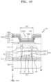
- FIG. 9 is a plan view schematically illustrating a display panel included in a display apparatus according to an embodiment.
- FIG. 10 is a schematic cross-sectional view of the display panel taken along line II-II' of FIG. 9 .
- the display panel 10 may include the display area DA and the peripheral area DPA outside of or adjacent to the display area DA.
- the display panel 10 may provide an image by using pixels P arranged or disposed in the display area DA.
- the pixels P may be implemented as a display element such as an organic light-emitting diode OLED. Each pixel P may emit, for example, light of a red color, a green color, a blue color or a white color.
- the display area DA may be covered or overlapped using an encapsulation member to be protected from external air or moisture or the like within the scope of the disclosure. However, embodiments are not limited thereto.
- a first flexible film 14 may be attached to a boundary at one or a side of the display panel 10. One or a side of the first flexible film 14 may be attached to the boundary at the one side of the display panel 10 by using an anisotropic conductive film.
- the first flexible film 14 may be a bendable flexible film.
- a display driver 12 may be arranged or disposed on the first flexible film 14.
- the display driver 12 may receive control signals and power voltages, and may generate signals and voltages for driving the display panel 10 and output the same.
- the display driver 12 may be formed using an integrated circuit (IC).
- a display circuit board 11 may be attached or disposed to the other or another side of the first flexible film 14.
- the other side of the first flexible film 14 may be attached to an upper surface of the display circuit board 11 by using an anisotropic conductive film.
- the display circuit board 11 may be a flexible printed circuit board (FPCB) that may be bendable, a rigid PCB that may be rigid and not easily bendable, or a complex PCB including both a rigid PCB and a flexible FPCB.
- FPCB flexible printed circuit board
- a touch sensor driver 13 may be arranged or disposed on the display circuit board 11.
- the touch sensor driver 13 may be formed using an IC.
- the touch sensor driver 13 may be attached to the display circuit board 11.
- the touch sensor driver 13 may be electrically connected to touch electrodes of a touch screen layer 400 ( FIG. 11 ) of the display panel 10 via the display circuit board 11.
- the touch screen layer of the display panel 10 may detect a touch input by a user by using at least one of various touch methods such as a resistive film type method, a capacitive type method, and the like within the scope of the disclosure. However, embodiments are not limited thereto.
- the touch sensor driver 13 may apply driving signals to driving electrodes among the touch electrodes. Then, whether the user has touched or not may be determined by detecting voltages charged in mutual capacitance between the driving electrodes and sensing electrodes, by using the sensing electrodes from among the touch electrodes.
- a touch by a user may include a contact touch and a proximity touch.
- a contact touch may refer to a direct contact by a user's finger or an object such as a pen, on the cover window 700 arranged or disposed on the touch screen layer.
- a proximity touch may refer to an approach by the finger of a user or an object such as a pen in proximity to the cover window 700.
- the touch sensor driver 13 may transmit sensor data to a main processor based on the detected voltages, and by analyzing the sensor data, the main processor may calculate touch coordinates where a touch input has occurred.
- a power supply unit for supplying driving voltages to drive the pixels P of the display panel 10, a scan driver, and the display driver 12 may be further arranged or disposed on the display circuit board 11.
- the power supply unit may be combined with the display driver 12, and as an example, the display driver 12 and the power supply unit may be formed using a single IC.
- a substrate 100 may include an insulating material such as glass, quartz, a polymer resin, or the like within the scope of the disclosure. However, embodiments are not limited thereto.
- the substrate 100 may include a polymer resin such as polyethersulfone, polyacrylate, polyetherimide, polyethylene naphthalate, polyethylene terephthalate, polyphenylene sulfide, polyarylate, PI, polycarbonate or cellulose acetate propionate.
- the substrate 100 may have a multi-layer structure including a layer including the above-described polymer resin and an inorganic layer (not shown).
- the substrate 100 may include two layers including the above-described polymer resin and an inorganic barrier layer therebetween.
- the substrate 100 may be a rigid substrate or a flexible substrate that may be bendable, foldable, or rollable.
- a buffer layer 111 may be located or disposed on the substrate 100 and reduce or prevent penetration of foreign substances, moisture, or external air from below the substrate 100 and provide a flat surface on the substrate 100.
- the buffer layer 111 may include an inorganic material such as an oxide or nitride, an organic material, or an organic-inorganic composite material, and may have a single-layer or multi-layer structure of an inorganic material and an organic material.
- a barrier layer (not shown) blocking penetration of outside air may be further included between the substrate 100 and the buffer layer 111.
- the buffer layer 111 may be formed of silicon oxide (SiO 2 ) or silicon nitride (SiNx).
- the buffer layer 111 may include a first buffer layer 111a and a second buffer layer 111b that may be stacked.
- the first buffer layer 111a may include silicon oxide (SiO 2 )
- the second buffer layer 111b may include silicon nitride (SiNx).
- the first buffer layer 11 1a may include silicon nitride (SiNx)
- the second buffer layer 111b may include silicon oxide (SiO 2 ).
- the first buffer layer 111a and the second buffer layer 111b may include a same or similar material.
- a pixel circuit PC may be arranged or disposed on the buffer layer 111.
- the pixel circuit PC may include a thin film transistor TFT and a storage capacitor Cst.
- the thin film transistor TFT may be arranged or disposed on the buffer layer 111.
- the thin film transistor TFT may include a semiconductor layer A, a gate electrode G, a source electrode S, and a drain electrode D.
- the thin film transistor TFT may be electrically connected to an organic light-emitting diode OLED to drive the organic light-emitting diode OLED.
- the semiconductor layer A may be arranged or disposed on the buffer layer 111 and may include polysilicon.
- the semiconductor layer A may include amorphous silicon.
- the semiconductor layer A may include an oxide of at least one material selected from the group including indium (In), gallium (Ga), stannum (Sn), zirconium (Zr), vanadium (V), hafnium (Hf), cadmium (Cd), germanium (Ge), chromium (Cr), titanium (Ti), and zinc (Zn).
- the semiconductor layer A may include a channel area and a source area and a drain area that may be doped with impurities.
- a first insulating layer 112 may be included to cover or overlap the semiconductor layer A.
- the first insulating layer 112 may include an inorganic insulating material such as silicon oxide (SiOx), silicon nitride (SiNx), silicon oxynitride (SiOxNy), aluminum oxide (Al 2 O 3 ), titanium oxide (TiO 2 ), tantalum oxide (Ta 2 O 5 ), hafnium oxide (HfO 2 ), zinc oxide (ZnO 2 ), or the like within the scope of the disclosure.
- the first insulating layer 112 may be a single layer or multiple layers including the above-described inorganic insulating materials.
- the gate electrode G may be arranged or disposed on the first insulating layer 112 to overlap the semiconductor layer A.
- the gate electrode G may include molybdenum (Mo), aluminum (Al), copper (Cu), titanium (Ti), and the like, and may include a single layer or multiple layers. In an embodiment, the gate electrode G may be a single layer of molybdenum (Mo).
- the second insulating layer 113 may cover or overlap the gate electrode G.
- the second insulating layer 113 may include an inorganic insulating material such as silicon oxide (SiOx), silicon nitride (SiN X ), silicon oxynitride (SiO X N Y ), aluminum oxide (Al 2 O 3 ), titanium oxide (TiO 2 ), tantalum oxide (Ta 2 O 5 ), hafnium oxide (HfO 2 ), zinc oxide (ZnO 2 ), or the like within the scope of the disclosure.
- the second insulating layer 113 may be a single layer or multiple layers including the above-described inorganic insulating materials.
- An upper electrode CE2 of the storage capacitor Cst may be arranged or disposed on the second insulating layer 113.
- the upper electrode CE2 arranged or disposed on the second insulating layer 113 may overlap the gate electrode G arranged or disposed under or below the second insulating layer 113.
- the gate electrode G and the upper electrode CE2 overlapping each other with the second insulating layer 113 therebetween may form the storage capacitor Cst.
- the gate electrode G may be a lower electrode CE1 of the storage capacitor Cst.
- the lower electrode CE1 of the storage capacitor Cst may be included as an independent component. In this case, the lower electrode CE1 and the gate electrode G may be spaced apart from each other by a certain or predetermined distance.
- the upper electrode CE2 may include aluminum (Al), platinum (Pt), palladium (Pd), silver (Ag), magnesium (Mg), gold (Au), nickel (Ni), neodymium (Nd), iridium (Ir), chromium (Cr), calcium (Ca), molybdenum (Mo), titanium (Ti), tungsten (W), and/or copper (Cu), and may include a single layer or multiple layers including the above-described materials.
- a third insulating layer 115 may cover or overlap the upper electrode CE2.
- the third insulating layer 115 may include an inorganic insulating material such as silicon oxide (SiOx), silicon nitride (SiN X ), silicon oxynitride (SiO X N Y ), aluminum oxide (Al 2 O 3 ), titanium oxide (TiO 2 ), tantalum oxide (Ta 2 O 5 ), hafnium oxide (HfO 2 ), zinc oxide (ZnO 2 ), or the like within the scope of the disclosure. However, embodiments are not limited thereto.
- the third insulating layer 115 may include a single layer or multiple layers including the above-described inorganic insulating materials.
- the first insulating layer 112, the second insulating layer 113, and the third insulating layer 115 may be collectively be referred to as insulating layers IIL.
- a source electrode S and a drain electrode D may be arranged or disposed on the third insulating layer 115.
- the source electrode S and the drain electrode D may include a conductive material including molybdenum (Mo), aluminum (Al), copper (Cu), titanium (Ti), and the like, and may be formed as a multi-layer or single-layer structure including the above materials.
- the source electrode S and the drain electrode D may have a multi-layer structure including titanium (Ti)/aluminum (Al)/titanium (Ti).
- a planarization layer 117 may be arranged or disposed on the source electrode S and the drain electrode D.
- the planarization layer 117 may have a flat upper surface such that a pixel electrode 121 arranged or disposed thereon may be flat.
- the planarization layer 117 may include an organic material or an inorganic material and may have a single-layer structure or a multi-layer structure.
- the planarization layer 117 may include a general-purpose polymer such as benzocyclobutene (BCB), PI, hexamethyldisiloxane (HMDSO), polymethylmethacrylate (PMMA), or polystyrene (PS), a polymer derivative having a phenolic group, acrylic polymer, imide-based polymer, aryl ether-based polymer, amide-based polymer, fluorine-based polymer, p-xylene-based polymer, or vinyl alcohol-based polymer.
- BCB benzocyclobutene
- HMDSO hexamethyldisiloxane
- PMMA polymethylmethacrylate
- PS polystyrene
- a polymer derivative having a phenolic group acrylic polymer, imide-based polymer, aryl ether-based polymer,
- the planarization layer 117 may include an inorganic insulating material such as silicon oxide (SiO X ), silicon nitride (SiN X ), silicon oxynitride (SiO X N Y ), aluminum oxide (Al 2 O 3 ), titanium oxide (TiO 2 ), tantalum oxide (Ta 2 O 5 ), hafnium oxide (HfO 2 ), zinc oxide (ZnO 2 ), or the like within the scope of the disclosure.
- an inorganic insulating material such as silicon oxide (SiO X ), silicon nitride (SiN X ), silicon oxynitride (SiO X N Y ), aluminum oxide (Al 2 O 3 ), titanium oxide (TiO 2 ), tantalum oxide (Ta 2 O 5 ), hafnium oxide (HfO 2 ), zinc oxide (ZnO 2 ), or the like within the scope of the disclosure.
- embodiments are not limited thereto.
- the planarization layer 117 may have a via hole exposing one of the source electrode S and the drain electrode D of the thin film transistor TFT, and the pixel electrode 121 may electrically contact the source electrode S or the drain electrode D via the via hole to be electrically connected to the thin film transistor TFT.
- planarization layer While one planarization layer is illustrated in FIG. 10 , in an embodiment, two planarization layers may also be included. Two planarization layers may be more advantageous in terms of a higher level of integration.
- the pixel electrode 121 may be arranged or disposed on the planarization layer 117.
- the pixel electrode 121 may include a conductive oxide such as indium tin oxide (ITO), indium zinc oxide (IZO), zinc oxide (ZnO), indium oxide (In 2 O 3 ), indium gallium oxide (IGO) or aluminum zinc oxide (AZO).
- the pixel electrode 121 may include a reflective layer including silver (Ag), magnesium (Mg), aluminum (Al), platinum (Pt), palladium (Pd), gold (Au), nickel (Ni), neodymium (Nd), iridium (Ir), chromium (Cr), or a compound thereof.
- the pixel electrode 121 may have a structure in which layers including ITO, IZO, ZnO or In 2 O 3 may be above or below the above-described reflective layer.
- the pixel electrode 121 may have a structure in which indium tin oxide (ITO)/ silver (Ag)/indium tin oxide (ITO) may be stacked.
- a pixel defining layer 119 may be arranged or disposed on the planarization layer 117.
- the pixel defining layer 119 may be arranged or disposed on the planarization layer 117 and cover or overlap edges of the pixel electrode 121.
- a first opening OP1 exposing at least a portion of the pixel electrode 121 may be defined or formed.
- An emission area EA of the organic light-emitting diode OLED, for example, a size and shape of a pixel P may be defined or formed by the first opening OP1.
- the pixel defining layer 119 may increase a distance between the edges of the pixel electrode 121 and an opposite electrode 123 above the pixel electrode 121 to thereby prevent an arc or the like at the edges of the pixel electrode 121.
- the pixel defining layer 119 may include, for example, an organic insulating material such as PI, polyamide, an acrylic resin, benzocylcobutene, HMDSO, a phenolic resin, or the like, and may be formed by spin coating or the like within the scope of the disclosure. However, embodiments are not limited thereto.
- a spacer to prevent mask stamping may be further arranged or disposed on the pixel defining layer 119.
- the spacer may be formed as a single body with the pixel defining layer 119.
- the spacer and the pixel defining layer 119 may be simultaneously formed in a same process by using a halftone mask process.
- An emission layer 122b may be arranged or disposed in the first opening OP1 defined or formed in the pixel defining layer 119, to correspond to the pixel electrode 121.
- the emission layer 122b may include a polymer material or a low-molecular material, and may emit light of red, green, blue or white color.
- An organic functional layer 122e may be arranged or disposed on and/or under or below the emission layer 122b.
- the organic functional layer 122e may include a first functional layer 122a and/or a second functional layer 122c.
- the first functional layer 122a or the second functional layer 122c may be omitted.
- the first functional layer 122a may be arranged or disposed under or below the emission layer 122b.
- the first functional layer 122a may have a single-layer or multi-layer structure including an organic material.
- the first functional layer 122a may be a hole transport layer (HTL) having a single-layer structure.
- the first functional layer 122a may include a hole injection layer (HIL) and a HTL.
- the first functional layer 122a may be formed as a single body to correspond to organic light-emitting diodes OLED included in the display area DA.
- the second functional layer 122c may be arranged or disposed on the emission layer 122b.
- the second functional layer 122c may be a single layer or multiple layers including an organic material.
- the second functional layer 122c may include an electron transport layer (ETL) and/or an electron injection layer (EIL).
- ETL electron transport layer
- EIL electron injection layer
- the second functional layer 122c may be formed as a single body to correspond to organic light-emitting diodes OLED included in the display area DA.
- the opposite electrode 123 may be arranged or disposed on the second functional layer 122c.
- the opposite electrode 123 may include a conductive material having a low work function.
- the opposite electrode 123 may include a (semi)transparent layer including silver (Ag), magnesium (Mg), aluminum (Al), platinum (Pt), palladium (Pd), gold (Au), nickel (Ni), neodymium (Nd), iridium (Ir), chromium (Cr), lithium (Li), calcium (Ca), or an alloy thereof.
- the opposite electrode 123 may further include a layer such as ITO, IZO, ZnO or In 2 O 3 on the (semi)transparent layer including the above-described materials.
- the opposite electrode 123 may be formed as a single body to correspond to organic light-emitting diodes OLED included in the display area DA.
- the layers from the pixel electrode 121 to the opposite electrode 123 may constitute an organic light-emitting diode OLED.
- An upper layer 150 including an organic material may be formed or disposed on the opposite electrode 123.
- the upper layer 150 may be provided to protect the opposite electrode 123 and also increase light extraction efficiency.
- the upper layer 150 may include an organic material having a higher refractive index than the opposite electrode 123.
- the upper layer 150 may include layers having different refractive indices and stacked on each other.
- the upper layer 150 may be formed by stacking a high-refractive index layer/low-refractive index layer/high-refractive index layer.
- a refractive index of the high-refractive index layer may be about 1.7 or higher, and a refractive index of the low-refractive index layer may be about 1.3 or lower.
- the upper layer 150 may further include LiF.
- the upper layer 150 may further include an inorganic insulating material such as silicon oxide (SiO 2 ) or silicon nitride (SiNx).
- the upper layer 150 may be omitted.
- description will focus on an embodiment in which the upper layer 150 may be arranged or disposed on the opposite electrode 123.
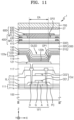
- FIG. 11 is a schematic cross-sectional view schematically illustrating a display apparatus according to an embodiment.
- like reference numerals as those in FIG. 10 denote like elements, and thus repeated description thereof will be omitted.
- a thin-film encapsulation layer 300 may be arranged or disposed on the organic light-emitting diode OLED.
- the thin-film encapsulation layer 300 may include at least one inorganic film layer and at least one organic film layer.
- the thin-film encapsulation layer 300 may include a first inorganic film layer 310, an organic film layer 320, and a second inorganic film layer 330.
- the first inorganic film layer 310 and the second inorganic film layer 330 may each include one or more inorganic insulating materials.
- the inorganic insulating material may include silicon oxide (SiOx), silicon nitride (SiNx), silicon oxynitride (SiOxNy), aluminum oxide (Al 2 O 3 ), titanium oxide (TiO 2 ), tantalum oxide (Ta 2 O 5 ), hafnium oxide (HfO 2 ), zinc oxide (ZnO 2 ), or the like within the scope of the disclosure.
- SiOx silicon oxide
- SiNx silicon nitride
- SiOxNy silicon oxynitride
- Al 2 O 3 aluminum oxide
- zinc oxide (ZnO 2 ) or the like within the scope of the disclosure.
- embodiments are not limited thereto.
- the organic film layer 320 may include a polymer-based material.
- the polymer-based material may include an acrylic resin, an epoxy resin, PI, polyethylene, and the like within the scope of the disclosure.
- the organic film layer 320 may include an acrylic resin, such as polymethylmethacrylate, polyacrylic acid, and the like within the scope of the disclosure.
- the organic film layer 320 may be formed by hardening a monomer or applying a polymer.
- the touch screen layer 400 may be arranged or disposed on the thin-film encapsulation layer 300.
- the touch screen layer 400 may include a first conductive layer MTL1 and a second conductive layer MTL2 including a sensing electrode and/or a trace line or the like within the scope of the disclosure.
- a first touch insulating layer 410 may be arranged or disposed between the thin-film encapsulation layer 300 and the first conductive layer MTL1
- a second touch insulating layer 430 may be arranged or disposed between the first conductive layer MTL1 and the second conductive layer MTL2.
- the first conductive layer MTL1 and the second conductive layer MTL2 may include a conductive material.
- the conductive material may include molybdenum (Mo), aluminum (Al), copper (Cu), titanium (Ti), or the like, and may include multiple layers or a single layer including the above material.
- the first conductive layer MTL1 and the second conductive layer MTL2 may have a structure in which a titanium layer, an aluminum layer, and a titanium layer may be sequentially stacked (Ti/Al/Ti).
- the first touch insulating layer 410 and the second touch insulating layer 430 may include an inorganic insulating material and/or an organic insulating material.
- the inorganic insulating material may include silicon oxide (SiOx), silicon nitride (SiNx), silicon oxynitride (SiO X N Y ), aluminum oxide (Al 2 O 3 ), titanium oxide (TiO 2 ), tantalum oxide (Ta 2 O 5 ), hafnium oxide (HfO 2 ), zinc oxide (ZnO 2 ), or the like within the scope of the disclosure.
- the organic insulating material may include an acrylic organic material, an imide organic material, or the like within the scope of the disclosure.
- a filter plate 600 may be arranged or disposed on the touch screen layer 400 as an optical functional layer.
- the filter plate 600 may include a black matrix 610, a color filter 620, and an overcoat layer 630.
- the black matrix 610 may be located or disposed in a non-emission area around the emission area EA and surround the emission area EA.
- the black matrix 610 may passivate a touch electrode of the touch screen layer 400.
- the second conductive layer MTL2 of the touch screen layer 400 may overlap the black matrix 610, and the second conductive layer MTL2 may be covered or overlapped using the black matrix 610.
- the black matrix 610 may include an insulating material (for example, an organic insulating material) including a pigment or dye having a black color.
- the black matrix 610 may include a material that may be included in the pixel defining layer 119.
- the black matrix 610 may have a second opening OP2 corresponding to the emission area EA.
- the second opening OP2 defined or formed in the black matrix 610 may be formed to be the same in size as or larger than the first opening OP1 defined or formed in the pixel defining layer 119.
- the color filter 620 may be arranged or disposed in the emission area EA of the organic light-emitting diode OLED.
- the color filter 620 may have a red, green, or blue pigment or dye according to a color of light emitted from the organic light-emitting diode OLED.
- the overcoat layer 630 covering or overlapping the black matrix 610 and the color filter 620 to planarize an upper surface of the filter plate 600 may be arranged or disposed on the black matrix 610 and the color filter 620.
- an optical functional layer including a polarization plate may be arranged or disposed on the touch screen layer 400.
- the optical functional layer may include an anti-reflection layer.
- the anti-reflection layer may reduce a reflectance of light (external light) incident from the outside to the display apparatus 1.
- the anti-reflection layer may include a polarization film.
- the polarization film may include a linear polarization plate and a phase delay film such as a quarter-wave ( ⁇ /4) plate.
- the phase delay film may be arranged or disposed on the touch screen layer 400, and a linear polarization plate may be arranged or disposed on the phase delay film.
- the anti-reflection layer may include a destructive interference structure.
- the destructive interference structure may include a first reflective layer and a second reflective layer arranged or disposed on different layers from each other. First reflected light and second reflected light respectively reflected by the first reflective layer and the second reflective layer may undergo destructive interference, thereby reducing external light reflectance.
- the cover window 700 may be arranged or disposed above the filter plate 600.
- the cover window 700 may be attached to the filter plate 600 by using the sixth adhesive layer 27.
- the sixth adhesive layer 27 may be a PSA or an OCA.
- the digitizer 40 may be arranged or disposed below the display panel 10, various input methods using a pen or the like may be provided to users.
- the sagging prevention member 80 may be arranged or disposed to correspond to the folding area FA, and a digitizer (for example, the third digitizer 40c) may be arranged or disposed above the sagging prevention member 80, various input methods using a pen or the like may be provided to users in the folding area FA.
- a digitizer for example, the third digitizer 40c
- a folding structure may be included in the second portion 30b of the plate 30 arranged or disposed below the display panel 10, the second portion 30b corresponding to the folding area FA, in-folding may be easily implemented.
- embodiments can provide a display apparatus comprising: a display area and a folding area; a display panel; a digitizer disposed below the display panel; a sagging prevention member disposed below the display panel overlapping the folding area.
- the display apparatus may fold in the folding area.
- the display panel may fold about a folding axis in the folding area.
- the display area and the folding area may correspond to portions of the display panel.
- a portion of the digitizer overlaps the folding area.
- the sagging prevention member may be arranged to prevent sagging of the display panel in the folding area.
- the display apparatus further comprises a lower cover disposed below the sagging prevention member.
- the sagging prevention member may be connected to the lower cover.
- the display area includes a first display area and a second display area spaced apart from each other, the folding area is disposed between the first display area and the second display area, and the digitizer includes a first digitizer overlapping the first display area, a second digitizer overlapping the second display area, and a third digitizer overlapping the folding area.
- the first digitizer and the second digitizer are spaced apart from each other.
- the third digitizer is disposed between the first digitizer and the second digitizer.
- the third digitizer is spaced apart from each of the first digitizer and the second digitizer.
- the third digitizer may be disposed above the sagging prevention member.
- the display apparatus further comprises a plate disposed between the display panel and the digitizer.
- the plate may include a first portion overlapping the display area; and a second portion overlapping the folding area.
- the first portion of the plate may include a non-metallic material, and the second portion of the plate may include a metallic material.
- the display apparatus may further comprise a folding structure disposed in the second portion of the plate.
- the display apparatus further comprises an electromagnetic wave absorption layer disposed below the digitizer.
- the electromagnetic wave absorption layer includes a first electromagnetic wave absorption layer overlapping the first display area, a second electromagnetic wave absorption layer overlapping the second display area, and a third electromagnetic wave absorption layer overlapping the folding area.
- the first electromagnetic wave absorption layer, the second electromagnetic wave absorption layer, and the third electromagnetic wave absorption layer may be spaced apart from one another.
- the third electromagnetic wave absorption layer may be disposed between the sagging prevention member and the third digitizer.
- the display apparatus further comprises a wing plate disposed below the electromagnetic wave absorption layer.
- the wing plate includes a first wing plate overlapping the first display area, and a second wing plate overlapping the second display area.
- the first wing plate and the second wing plate may be spaced apart from each other.
- the sagging prevention member is disposed between the first wing plate and the second wing plate.
- the display apparatus may further comprise an optical functional layer disposed above the display panel.
- the display apparatus further comprises a plate disposed below the display panel and comprising a first portion overlapping the display area, and a second portion overlapping the folding area, wherein the digitizer is disposed below the plate, and wherein the sagging prevention member is disposed below the plate overlapping the folding area.
- the first portion of the plate and the second portion of the plate may include different materials.
- the first digitizer and the second digitizer overlap the first portion of the plate, and the third digitizer overlaps the second portion of the plate.
- the third digitizer may be disposed above the sagging prevention member.
- the display apparatus comprises a wing plate disposed below the digitizer, wherein the wing plate includes a first wing plate overlapping the first display area, and a second wing plate overlapping the second display area.
- the first wing plate and the second wing plate may be spaced apart from each other.
- the sagging prevention member may be disposed between the first wing plate and the second wing plate.
- the display apparatus further comprises a cushion layer disposed above the wing plate, wherein the cushion layer includes a first cushion layer overlapping the first display area, and a second cushion layer overlapping the second display area.
- the first cushion layer and the second cushion layer may be spaced apart from each other.
- the sagging prevention member may be disposed between the first cushion layer and the second cushion layer.
- a digitizer may be included below a foldable display panel that may be folded or unfolded, various input methods using a pen or the like may be provided to users.
- the scope of the disclosure is not limited by the above-described effects.
Landscapes
- Engineering & Computer Science (AREA)
- Theoretical Computer Science (AREA)
- Computer Hardware Design (AREA)
- Physics & Mathematics (AREA)
- General Physics & Mathematics (AREA)
- General Engineering & Computer Science (AREA)
- Human Computer Interaction (AREA)
- Mathematical Physics (AREA)
- Signal Processing (AREA)
- Devices For Indicating Variable Information By Combining Individual Elements (AREA)
- Facsimiles In General (AREA)
- Fittings On The Vehicle Exterior For Carrying Loads, And Devices For Holding Or Mounting Articles (AREA)
Applications Claiming Priority (2)
| Application Number | Priority Date | Filing Date | Title |
|---|---|---|---|
| KR1020200113218A KR20220031838A (ko) | 2020-09-04 | 2020-09-04 | 표시 장치 |
| EP21180159.2A EP3964920B1 (de) | 2020-09-04 | 2021-06-17 | Faltbare anzeigevorrichtung |
Related Parent Applications (2)
| Application Number | Title | Priority Date | Filing Date |
|---|---|---|---|
| EP21180159.2A Division EP3964920B1 (de) | 2020-09-04 | 2021-06-17 | Faltbare anzeigevorrichtung |
| EP21180159.2A Division-Into EP3964920B1 (de) | 2020-09-04 | 2021-06-17 | Faltbare anzeigevorrichtung |
Publications (3)
| Publication Number | Publication Date |
|---|---|
| EP4231613A2 true EP4231613A2 (de) | 2023-08-23 |
| EP4231613A3 EP4231613A3 (de) | 2023-09-06 |
| EP4231613B1 EP4231613B1 (de) | 2024-09-11 |
Family
ID=76522835
Family Applications (2)
| Application Number | Title | Priority Date | Filing Date |
|---|---|---|---|
| EP23185403.5A Active EP4231613B1 (de) | 2020-09-04 | 2021-06-17 | Faltbare anzeigevorrichtung |
| EP21180159.2A Active EP3964920B1 (de) | 2020-09-04 | 2021-06-17 | Faltbare anzeigevorrichtung |
Family Applications After (1)
| Application Number | Title | Priority Date | Filing Date |
|---|---|---|---|
| EP21180159.2A Active EP3964920B1 (de) | 2020-09-04 | 2021-06-17 | Faltbare anzeigevorrichtung |
Country Status (4)
| Country | Link |
|---|---|
| US (2) | US11513555B2 (de) |
| EP (2) | EP4231613B1 (de) |
| KR (1) | KR20220031838A (de) |
| CN (2) | CN114141136B (de) |
Families Citing this family (14)
| Publication number | Priority date | Publication date | Assignee | Title |
|---|---|---|---|---|
| KR102937328B1 (ko) * | 2020-09-21 | 2026-03-11 | 삼성디스플레이 주식회사 | 표시장치 |
| KR102941495B1 (ko) | 2020-11-13 | 2026-03-19 | 삼성디스플레이 주식회사 | 표시 장치 |
| KR102919521B1 (ko) * | 2020-12-10 | 2026-01-29 | 삼성디스플레이 주식회사 | 표시 장치 |
| KR20220093624A (ko) | 2020-12-28 | 2022-07-05 | 엘지디스플레이 주식회사 | 폴더블 표시 장치 |
| KR102923423B1 (ko) * | 2021-01-27 | 2026-02-05 | 삼성디스플레이 주식회사 | 표시 장치 |
| KR20230025598A (ko) * | 2021-08-13 | 2023-02-22 | 삼성디스플레이 주식회사 | 표시 장치 |
| KR20230038853A (ko) * | 2021-09-13 | 2023-03-21 | 엘지디스플레이 주식회사 | 폴더블 디스플레이 장치 |
| KR20230121667A (ko) * | 2022-02-11 | 2023-08-21 | 삼성디스플레이 주식회사 | 표시 장치 |
| US11917780B2 (en) * | 2022-03-08 | 2024-02-27 | Microsoft Technology Licensing, Llc | Hinged device with a flexible display |
| KR20240029633A (ko) | 2022-08-25 | 2024-03-06 | 삼성디스플레이 주식회사 | 표시장치 및 이를 포함하는 전자장치 |
| KR20240080307A (ko) | 2022-11-29 | 2024-06-07 | 삼성디스플레이 주식회사 | 표시장치 및 표시장치의 제조방법 |
| US12596410B2 (en) * | 2022-12-28 | 2026-04-07 | Lg Electronics Inc. | Portable electronic device |
| KR20250019770A (ko) * | 2023-08-01 | 2025-02-11 | 삼성디스플레이 주식회사 | 전자장치 |
| KR20260008901A (ko) * | 2024-07-09 | 2026-01-19 | 삼성디스플레이 주식회사 | 표시장치 |
Family Cites Families (23)
| Publication number | Priority date | Publication date | Assignee | Title |
|---|---|---|---|---|
| KR20170077670A (ko) | 2015-12-28 | 2017-07-06 | 삼성전자주식회사 | 컨텐츠를 제어하기 위한 방법 및 그 전자 장치 |
| KR102494986B1 (ko) | 2016-01-11 | 2023-02-03 | 삼성디스플레이 주식회사 | 폴더블 표시장치 |
| WO2018213687A2 (en) * | 2017-05-19 | 2018-11-22 | E Ink Corporation | Foldable electro-optic display including digitization and touch sensing |
| CN108335633B (zh) * | 2018-01-19 | 2021-02-09 | 云谷(固安)科技有限公司 | 一种柔性显示屏、显示装置 |
| KR102452238B1 (ko) * | 2018-05-11 | 2022-10-07 | 삼성디스플레이 주식회사 | 표시 장치 |
| KR102457059B1 (ko) * | 2018-05-11 | 2022-10-20 | 삼성디스플레이 주식회사 | 표시 장치 |
| KR102586636B1 (ko) * | 2018-10-11 | 2023-10-11 | 삼성디스플레이 주식회사 | 폴더블 표시장치 |
| US11096293B2 (en) * | 2018-10-26 | 2021-08-17 | Samsung Display Co., Ltd. | Electronic device and display device applied to the same |
| US10592051B1 (en) * | 2018-10-31 | 2020-03-17 | Dell Products, L.P. | Touch input correction for multi-form factor information handling system (IHS) |
| KR102639547B1 (ko) * | 2019-01-02 | 2024-02-26 | 삼성디스플레이 주식회사 | 표시 장치 |
| KR102577249B1 (ko) * | 2019-01-21 | 2023-09-12 | 삼성전자주식회사 | 자석 및 자석 차폐 부재를 포함하는 전자 장치 |
| KR102750020B1 (ko) * | 2019-06-24 | 2025-01-08 | 삼성디스플레이 주식회사 | 표시 장치 |
| KR102850924B1 (ko) * | 2019-08-02 | 2025-08-28 | 삼성디스플레이 주식회사 | 전자 장치 |
| KR20210016231A (ko) * | 2019-08-02 | 2021-02-15 | 삼성디스플레이 주식회사 | 패널 하부 시트 및 이를 포함하는 표시 장치 |
| KR102786913B1 (ko) * | 2019-12-10 | 2025-03-28 | 삼성디스플레이 주식회사 | 폴더블 표시 장치 및 그 구동 방법 |
| KR102831678B1 (ko) * | 2020-04-23 | 2025-07-09 | 삼성디스플레이 주식회사 | 플렉서블 표시장치 |
| KR102825013B1 (ko) * | 2020-04-28 | 2025-06-27 | 삼성디스플레이 주식회사 | 디지타이저 및 이를 포함하는 표시 장치 |
| KR20220006669A (ko) * | 2020-07-08 | 2022-01-18 | 삼성디스플레이 주식회사 | 표시 장치 |
| KR102937329B1 (ko) * | 2020-07-10 | 2026-03-11 | 삼성디스플레이 주식회사 | 디지타이저 및 표시 장치 |
| KR20220013766A (ko) * | 2020-07-27 | 2022-02-04 | 삼성전자주식회사 | 멀티 폴더블 전자 장치 |
| KR102866603B1 (ko) * | 2020-08-06 | 2025-10-01 | 삼성디스플레이 주식회사 | 전자 장치 및 이의 제조 방법 |
| KR20220019188A (ko) * | 2020-08-07 | 2022-02-16 | 삼성디스플레이 주식회사 | 표시 장치 |
| US11570911B2 (en) * | 2020-08-20 | 2023-01-31 | Samsung Display Co., Ltd. | Display device |
-
2020
- 2020-09-04 KR KR1020200113218A patent/KR20220031838A/ko active Pending
-
2021
- 2021-03-17 US US17/204,242 patent/US11513555B2/en active Active
- 2021-06-17 EP EP23185403.5A patent/EP4231613B1/de active Active
- 2021-06-17 EP EP21180159.2A patent/EP3964920B1/de active Active
- 2021-08-06 CN CN202110901642.9A patent/CN114141136B/zh active Active
- 2021-08-06 CN CN202610028283.3A patent/CN121789564A/zh active Pending
-
2022
- 2022-11-28 US US18/070,140 patent/US11762419B2/en active Active
Also Published As
| Publication number | Publication date |
|---|---|
| US11762419B2 (en) | 2023-09-19 |
| US11513555B2 (en) | 2022-11-29 |
| US20220075411A1 (en) | 2022-03-10 |
| US20230092852A1 (en) | 2023-03-23 |
| EP4231613B1 (de) | 2024-09-11 |
| EP3964920B1 (de) | 2024-01-17 |
| CN121789564A (zh) | 2026-04-03 |
| EP3964920A1 (de) | 2022-03-09 |
| CN114141136A (zh) | 2022-03-04 |
| CN114141136B (zh) | 2026-01-30 |
| KR20220031838A (ko) | 2022-03-14 |
| EP4231613A3 (de) | 2023-09-06 |
Similar Documents
| Publication | Publication Date | Title |
|---|---|---|
| EP4231613B1 (de) | Faltbare anzeigevorrichtung | |
| US11289684B2 (en) | Display device and electronic apparatus | |
| KR102937329B1 (ko) | 디지타이저 및 표시 장치 | |
| US11974461B2 (en) | Display apparatus | |
| US20230371346A1 (en) | Display device, electronic device including the same, and method of manufacturing the display device | |
| KR20220126326A (ko) | 디지타이저 및 표시 장치 | |
| KR20220166401A (ko) | 표시 패널 및 이를 포함하는 전자 기기 | |
| KR20230160664A (ko) | 표시 장치, 이를 포함하는 전자기기 및 표시 장치의 제조방법 | |
| KR20230061675A (ko) | 표시 장치 및 표시 장치의 제조방법 | |
| KR20220065976A (ko) | 표시 장치 | |
| US20240126344A1 (en) | Display apparatus | |
| US20240179974A1 (en) | Bending area structure of display apparatus and method of providing the same | |
| US12289962B2 (en) | Display panel and electronic apparatus | |
| CN117082921A (zh) | 显示装置、包括其的电子装置和制造显示装置的方法 | |
| CN223219446U (zh) | 显示设备 | |
| US20230269318A1 (en) | Protection panel and display apparatus including the same | |
| US12197690B2 (en) | Display device and method of manufacturing the same | |
| US20230403910A1 (en) | Display device | |
| US20260020480A1 (en) | Display apparatus | |
| KR20240144597A (ko) | 표시 장치 | |
| CN120726902A (zh) | 显示设备 |
Legal Events
| Date | Code | Title | Description |
|---|---|---|---|
| PUAI | Public reference made under article 153(3) epc to a published international application that has entered the european phase |
Free format text: ORIGINAL CODE: 0009012 |
|
| STAA | Information on the status of an ep patent application or granted ep patent |
Free format text: STATUS: REQUEST FOR EXAMINATION WAS MADE |
|
| REG | Reference to a national code |
Ref country code: DE Ref legal event code: R079 Ref document number: 602021018811 Country of ref document: DE Free format text: PREVIOUS MAIN CLASS: H04M0001020000 Ipc: G06F0001160000 Ref country code: DE Ref legal event code: R079 Free format text: PREVIOUS MAIN CLASS: H04M0001020000 Ipc: G06F0001160000 |
|
| PUAL | Search report despatched |
Free format text: ORIGINAL CODE: 0009013 |
|
| 17P | Request for examination filed |
Effective date: 20230713 |
|
| AC | Divisional application: reference to earlier application |
Ref document number: 3964920 Country of ref document: EP Kind code of ref document: P |
|
| AK | Designated contracting states |
Kind code of ref document: A2 Designated state(s): AL AT BE BG CH CY CZ DE DK EE ES FI FR GB GR HR HU IE IS IT LI LT LU LV MC MK MT NL NO PL PT RO RS SE SI SK SM TR |
|
| AK | Designated contracting states |
Kind code of ref document: A3 Designated state(s): AL AT BE BG CH CY CZ DE DK EE ES FI FR GB GR HR HU IE IS IT LI LT LU LV MC MK MT NL NO PL PT RO RS SE SI SK SM TR |
|
| RIC1 | Information provided on ipc code assigned before grant |
Ipc: H04M 1/02 20060101ALI20230731BHEP Ipc: G06F 1/16 20060101AFI20230731BHEP |
|
| GRAP | Despatch of communication of intention to grant a patent |
Free format text: ORIGINAL CODE: EPIDOSNIGR1 |
|
| STAA | Information on the status of an ep patent application or granted ep patent |
Free format text: STATUS: GRANT OF PATENT IS INTENDED |
|
| INTG | Intention to grant announced |
Effective date: 20240404 |
|
| GRAS | Grant fee paid |
Free format text: ORIGINAL CODE: EPIDOSNIGR3 |
|
| GRAA | (expected) grant |
Free format text: ORIGINAL CODE: 0009210 |
|
| STAA | Information on the status of an ep patent application or granted ep patent |
Free format text: STATUS: THE PATENT HAS BEEN GRANTED |
|
| AC | Divisional application: reference to earlier application |
Ref document number: 3964920 Country of ref document: EP Kind code of ref document: P |
|
| AK | Designated contracting states |
Kind code of ref document: B1 Designated state(s): AL AT BE BG CH CY CZ DE DK EE ES FI FR GB GR HR HU IE IS IT LI LT LU LV MC MK MT NL NO PL PT RO RS SE SI SK SM TR |
|
| REG | Reference to a national code |
Ref country code: GB Ref legal event code: FG4D |
|
| REG | Reference to a national code |
Ref country code: CH Ref legal event code: EP |
|
| REG | Reference to a national code |
Ref country code: DE Ref legal event code: R096 Ref document number: 602021018811 Country of ref document: DE |
|
| REG | Reference to a national code |
Ref country code: IE Ref legal event code: FG4D |
|
| REG | Reference to a national code |
Ref country code: LT Ref legal event code: MG9D |
|
| PG25 | Lapsed in a contracting state [announced via postgrant information from national office to epo] |
Ref country code: NO Free format text: LAPSE BECAUSE OF FAILURE TO SUBMIT A TRANSLATION OF THE DESCRIPTION OR TO PAY THE FEE WITHIN THE PRESCRIBED TIME-LIMIT Effective date: 20241211 |
|
| PG25 | Lapsed in a contracting state [announced via postgrant information from national office to epo] |
Ref country code: GR Free format text: LAPSE BECAUSE OF FAILURE TO SUBMIT A TRANSLATION OF THE DESCRIPTION OR TO PAY THE FEE WITHIN THE PRESCRIBED TIME-LIMIT Effective date: 20241212 Ref country code: FI Free format text: LAPSE BECAUSE OF FAILURE TO SUBMIT A TRANSLATION OF THE DESCRIPTION OR TO PAY THE FEE WITHIN THE PRESCRIBED TIME-LIMIT Effective date: 20240911 |
|
| PG25 | Lapsed in a contracting state [announced via postgrant information from national office to epo] |
Ref country code: BG Free format text: LAPSE BECAUSE OF FAILURE TO SUBMIT A TRANSLATION OF THE DESCRIPTION OR TO PAY THE FEE WITHIN THE PRESCRIBED TIME-LIMIT Effective date: 20240911 |
|
| PG25 | Lapsed in a contracting state [announced via postgrant information from national office to epo] |
Ref country code: LV Free format text: LAPSE BECAUSE OF FAILURE TO SUBMIT A TRANSLATION OF THE DESCRIPTION OR TO PAY THE FEE WITHIN THE PRESCRIBED TIME-LIMIT Effective date: 20240911 |
|
| PG25 | Lapsed in a contracting state [announced via postgrant information from national office to epo] |
Ref country code: HR Free format text: LAPSE BECAUSE OF FAILURE TO SUBMIT A TRANSLATION OF THE DESCRIPTION OR TO PAY THE FEE WITHIN THE PRESCRIBED TIME-LIMIT Effective date: 20240911 |
|
| PG25 | Lapsed in a contracting state [announced via postgrant information from national office to epo] |
Ref country code: RS Free format text: LAPSE BECAUSE OF FAILURE TO SUBMIT A TRANSLATION OF THE DESCRIPTION OR TO PAY THE FEE WITHIN THE PRESCRIBED TIME-LIMIT Effective date: 20241211 Ref country code: ES Free format text: LAPSE BECAUSE OF FAILURE TO SUBMIT A TRANSLATION OF THE DESCRIPTION OR TO PAY THE FEE WITHIN THE PRESCRIBED TIME-LIMIT Effective date: 20240911 |
|
| PG25 | Lapsed in a contracting state [announced via postgrant information from national office to epo] |
Ref country code: RS Free format text: LAPSE BECAUSE OF FAILURE TO SUBMIT A TRANSLATION OF THE DESCRIPTION OR TO PAY THE FEE WITHIN THE PRESCRIBED TIME-LIMIT Effective date: 20241211 Ref country code: NO Free format text: LAPSE BECAUSE OF FAILURE TO SUBMIT A TRANSLATION OF THE DESCRIPTION OR TO PAY THE FEE WITHIN THE PRESCRIBED TIME-LIMIT Effective date: 20241211 Ref country code: LV Free format text: LAPSE BECAUSE OF FAILURE TO SUBMIT A TRANSLATION OF THE DESCRIPTION OR TO PAY THE FEE WITHIN THE PRESCRIBED TIME-LIMIT Effective date: 20240911 Ref country code: HR Free format text: LAPSE BECAUSE OF FAILURE TO SUBMIT A TRANSLATION OF THE DESCRIPTION OR TO PAY THE FEE WITHIN THE PRESCRIBED TIME-LIMIT Effective date: 20240911 Ref country code: GR Free format text: LAPSE BECAUSE OF FAILURE TO SUBMIT A TRANSLATION OF THE DESCRIPTION OR TO PAY THE FEE WITHIN THE PRESCRIBED TIME-LIMIT Effective date: 20241212 Ref country code: FI Free format text: LAPSE BECAUSE OF FAILURE TO SUBMIT A TRANSLATION OF THE DESCRIPTION OR TO PAY THE FEE WITHIN THE PRESCRIBED TIME-LIMIT Effective date: 20240911 Ref country code: ES Free format text: LAPSE BECAUSE OF FAILURE TO SUBMIT A TRANSLATION OF THE DESCRIPTION OR TO PAY THE FEE WITHIN THE PRESCRIBED TIME-LIMIT Effective date: 20240911 Ref country code: BG Free format text: LAPSE BECAUSE OF FAILURE TO SUBMIT A TRANSLATION OF THE DESCRIPTION OR TO PAY THE FEE WITHIN THE PRESCRIBED TIME-LIMIT Effective date: 20240911 |
|
| REG | Reference to a national code |
Ref country code: AT Ref legal event code: MK05 Ref document number: 1723255 Country of ref document: AT Kind code of ref document: T Effective date: 20240911 |
|
| PG25 | Lapsed in a contracting state [announced via postgrant information from national office to epo] |
Ref country code: NL Free format text: LAPSE BECAUSE OF FAILURE TO SUBMIT A TRANSLATION OF THE DESCRIPTION OR TO PAY THE FEE WITHIN THE PRESCRIBED TIME-LIMIT Effective date: 20240911 |
|
| PG25 | Lapsed in a contracting state [announced via postgrant information from national office to epo] |
Ref country code: PT Free format text: LAPSE BECAUSE OF FAILURE TO SUBMIT A TRANSLATION OF THE DESCRIPTION OR TO PAY THE FEE WITHIN THE PRESCRIBED TIME-LIMIT Effective date: 20250113 Ref country code: IS Free format text: LAPSE BECAUSE OF FAILURE TO SUBMIT A TRANSLATION OF THE DESCRIPTION OR TO PAY THE FEE WITHIN THE PRESCRIBED TIME-LIMIT Effective date: 20250111 |
|
| PG25 | Lapsed in a contracting state [announced via postgrant information from national office to epo] |
Ref country code: RO Free format text: LAPSE BECAUSE OF FAILURE TO SUBMIT A TRANSLATION OF THE DESCRIPTION OR TO PAY THE FEE WITHIN THE PRESCRIBED TIME-LIMIT Effective date: 20240911 Ref country code: SM Free format text: LAPSE BECAUSE OF FAILURE TO SUBMIT A TRANSLATION OF THE DESCRIPTION OR TO PAY THE FEE WITHIN THE PRESCRIBED TIME-LIMIT Effective date: 20240911 |
|
| PG25 | Lapsed in a contracting state [announced via postgrant information from national office to epo] |
Ref country code: EE Free format text: LAPSE BECAUSE OF FAILURE TO SUBMIT A TRANSLATION OF THE DESCRIPTION OR TO PAY THE FEE WITHIN THE PRESCRIBED TIME-LIMIT Effective date: 20240911 Ref country code: AT Free format text: LAPSE BECAUSE OF FAILURE TO SUBMIT A TRANSLATION OF THE DESCRIPTION OR TO PAY THE FEE WITHIN THE PRESCRIBED TIME-LIMIT Effective date: 20240911 |
|
| PG25 | Lapsed in a contracting state [announced via postgrant information from national office to epo] |
Ref country code: PL Free format text: LAPSE BECAUSE OF FAILURE TO SUBMIT A TRANSLATION OF THE DESCRIPTION OR TO PAY THE FEE WITHIN THE PRESCRIBED TIME-LIMIT Effective date: 20240911 Ref country code: CZ Free format text: LAPSE BECAUSE OF FAILURE TO SUBMIT A TRANSLATION OF THE DESCRIPTION OR TO PAY THE FEE WITHIN THE PRESCRIBED TIME-LIMIT Effective date: 20240911 |
|
| PG25 | Lapsed in a contracting state [announced via postgrant information from national office to epo] |
Ref country code: IT Free format text: LAPSE BECAUSE OF FAILURE TO SUBMIT A TRANSLATION OF THE DESCRIPTION OR TO PAY THE FEE WITHIN THE PRESCRIBED TIME-LIMIT Effective date: 20240911 Ref country code: SK Free format text: LAPSE BECAUSE OF FAILURE TO SUBMIT A TRANSLATION OF THE DESCRIPTION OR TO PAY THE FEE WITHIN THE PRESCRIBED TIME-LIMIT Effective date: 20240911 |
|
| REG | Reference to a national code |
Ref country code: DE Ref legal event code: R097 Ref document number: 602021018811 Country of ref document: DE |
|
| PGFP | Annual fee paid to national office [announced via postgrant information from national office to epo] |
Ref country code: DE Payment date: 20250520 Year of fee payment: 5 |
|
| PG25 | Lapsed in a contracting state [announced via postgrant information from national office to epo] |
Ref country code: DK Free format text: LAPSE BECAUSE OF FAILURE TO SUBMIT A TRANSLATION OF THE DESCRIPTION OR TO PAY THE FEE WITHIN THE PRESCRIBED TIME-LIMIT Effective date: 20240911 |
|
| PGFP | Annual fee paid to national office [announced via postgrant information from national office to epo] |
Ref country code: GB Payment date: 20250520 Year of fee payment: 5 |
|
| PGFP | Annual fee paid to national office [announced via postgrant information from national office to epo] |
Ref country code: FR Payment date: 20250521 Year of fee payment: 5 |
|
| PLBE | No opposition filed within time limit |
Free format text: ORIGINAL CODE: 0009261 |
|
| STAA | Information on the status of an ep patent application or granted ep patent |
Free format text: STATUS: NO OPPOSITION FILED WITHIN TIME LIMIT |
|
| 26N | No opposition filed |
Effective date: 20250612 |
|
| PG25 | Lapsed in a contracting state [announced via postgrant information from national office to epo] |
Ref country code: SE Free format text: LAPSE BECAUSE OF FAILURE TO SUBMIT A TRANSLATION OF THE DESCRIPTION OR TO PAY THE FEE WITHIN THE PRESCRIBED TIME-LIMIT Effective date: 20240911 |
|
| REG | Reference to a national code |
Ref country code: CH Ref legal event code: H13 Free format text: ST27 STATUS EVENT CODE: U-0-0-H10-H13 (AS PROVIDED BY THE NATIONAL OFFICE) Effective date: 20260127 |
|
| PG25 | Lapsed in a contracting state [announced via postgrant information from national office to epo] |
Ref country code: MC Free format text: LAPSE BECAUSE OF FAILURE TO SUBMIT A TRANSLATION OF THE DESCRIPTION OR TO PAY THE FEE WITHIN THE PRESCRIBED TIME-LIMIT Effective date: 20240911 |
|
| PG25 | Lapsed in a contracting state [announced via postgrant information from national office to epo] |
Ref country code: LU Free format text: LAPSE BECAUSE OF NON-PAYMENT OF DUE FEES Effective date: 20250617 |
|
| REG | Reference to a national code |
Ref country code: BE Ref legal event code: MM Effective date: 20250630 |
|
| PG25 | Lapsed in a contracting state [announced via postgrant information from national office to epo] |
Ref country code: IE Free format text: LAPSE BECAUSE OF NON-PAYMENT OF DUE FEES Effective date: 20250617 |
|
| PG25 | Lapsed in a contracting state [announced via postgrant information from national office to epo] |
Ref country code: BE Free format text: LAPSE BECAUSE OF NON-PAYMENT OF DUE FEES Effective date: 20250630 |
|
| PG25 | Lapsed in a contracting state [announced via postgrant information from national office to epo] |
Ref country code: CH Free format text: LAPSE BECAUSE OF NON-PAYMENT OF DUE FEES Effective date: 20250630 |