EP4213604B1 - Display substrate, manufactoring method therefor, and display device therewith - Google Patents
Display substrate, manufactoring method therefor, and display device therewith Download PDFInfo
- Publication number
- EP4213604B1 EP4213604B1 EP22831231.0A EP22831231A EP4213604B1 EP 4213604 B1 EP4213604 B1 EP 4213604B1 EP 22831231 A EP22831231 A EP 22831231A EP 4213604 B1 EP4213604 B1 EP 4213604B1
- Authority
- EP
- European Patent Office
- Prior art keywords
- sub
- pixel
- power supply
- layer
- signal line
- Prior art date
- Legal status (The legal status is an assumption and is not a legal conclusion. Google has not performed a legal analysis and makes no representation as to the accuracy of the status listed.)
- Active
Links
Images


Classifications
-
- G—PHYSICS
- G09—EDUCATION; CRYPTOGRAPHY; DISPLAY; ADVERTISING; SEALS
- G09G—ARRANGEMENTS OR CIRCUITS FOR CONTROL OF INDICATING DEVICES USING STATIC MEANS TO PRESENT VARIABLE INFORMATION
- G09G3/00—Control arrangements or circuits, of interest only in connection with visual indicators other than cathode-ray tubes
- G09G3/20—Control arrangements or circuits, of interest only in connection with visual indicators other than cathode-ray tubes for presentation of an assembly of a number of characters, e.g. a page, by composing the assembly by combination of individual elements arranged in a matrix no fixed position being assigned to or needed to be assigned to the individual characters or partial characters
- G09G3/22—Control arrangements or circuits, of interest only in connection with visual indicators other than cathode-ray tubes for presentation of an assembly of a number of characters, e.g. a page, by composing the assembly by combination of individual elements arranged in a matrix no fixed position being assigned to or needed to be assigned to the individual characters or partial characters using controlled light sources
- G09G3/30—Control arrangements or circuits, of interest only in connection with visual indicators other than cathode-ray tubes for presentation of an assembly of a number of characters, e.g. a page, by composing the assembly by combination of individual elements arranged in a matrix no fixed position being assigned to or needed to be assigned to the individual characters or partial characters using controlled light sources using electroluminescent panels
- G09G3/32—Control arrangements or circuits, of interest only in connection with visual indicators other than cathode-ray tubes for presentation of an assembly of a number of characters, e.g. a page, by composing the assembly by combination of individual elements arranged in a matrix no fixed position being assigned to or needed to be assigned to the individual characters or partial characters using controlled light sources using electroluminescent panels semiconductive, e.g. using light-emitting diodes [LED]
- G09G3/3208—Control arrangements or circuits, of interest only in connection with visual indicators other than cathode-ray tubes for presentation of an assembly of a number of characters, e.g. a page, by composing the assembly by combination of individual elements arranged in a matrix no fixed position being assigned to or needed to be assigned to the individual characters or partial characters using controlled light sources using electroluminescent panels semiconductive, e.g. using light-emitting diodes [LED] organic, e.g. using organic light-emitting diodes [OLED]
- G09G3/3225—Control arrangements or circuits, of interest only in connection with visual indicators other than cathode-ray tubes for presentation of an assembly of a number of characters, e.g. a page, by composing the assembly by combination of individual elements arranged in a matrix no fixed position being assigned to or needed to be assigned to the individual characters or partial characters using controlled light sources using electroluminescent panels semiconductive, e.g. using light-emitting diodes [LED] organic, e.g. using organic light-emitting diodes [OLED] using an active matrix
- G09G3/3233—Control arrangements or circuits, of interest only in connection with visual indicators other than cathode-ray tubes for presentation of an assembly of a number of characters, e.g. a page, by composing the assembly by combination of individual elements arranged in a matrix no fixed position being assigned to or needed to be assigned to the individual characters or partial characters using controlled light sources using electroluminescent panels semiconductive, e.g. using light-emitting diodes [LED] organic, e.g. using organic light-emitting diodes [OLED] using an active matrix with pixel circuitry controlling the current through the light-emitting element
-
- H—ELECTRICITY
- H10—SEMICONDUCTOR DEVICES; ELECTRIC SOLID-STATE DEVICES NOT OTHERWISE PROVIDED FOR
- H10D—INORGANIC ELECTRIC SEMICONDUCTOR DEVICES
- H10D86/00—Integrated devices formed in or on insulating or conducting substrates, e.g. formed in silicon-on-insulator [SOI] substrates or on stainless steel or glass substrates
- H10D86/40—Integrated devices formed in or on insulating or conducting substrates, e.g. formed in silicon-on-insulator [SOI] substrates or on stainless steel or glass substrates characterised by multiple TFTs
- H10D86/421—Integrated devices formed in or on insulating or conducting substrates, e.g. formed in silicon-on-insulator [SOI] substrates or on stainless steel or glass substrates characterised by multiple TFTs having a particular composition, shape or crystalline structure of the active layer
- H10D86/423—Integrated devices formed in or on insulating or conducting substrates, e.g. formed in silicon-on-insulator [SOI] substrates or on stainless steel or glass substrates characterised by multiple TFTs having a particular composition, shape or crystalline structure of the active layer comprising semiconductor materials not belonging to the Group IV, e.g. InGaZnO
-
- H—ELECTRICITY
- H10—SEMICONDUCTOR DEVICES; ELECTRIC SOLID-STATE DEVICES NOT OTHERWISE PROVIDED FOR
- H10D—INORGANIC ELECTRIC SEMICONDUCTOR DEVICES
- H10D86/00—Integrated devices formed in or on insulating or conducting substrates, e.g. formed in silicon-on-insulator [SOI] substrates or on stainless steel or glass substrates
- H10D86/40—Integrated devices formed in or on insulating or conducting substrates, e.g. formed in silicon-on-insulator [SOI] substrates or on stainless steel or glass substrates characterised by multiple TFTs
- H10D86/60—Integrated devices formed in or on insulating or conducting substrates, e.g. formed in silicon-on-insulator [SOI] substrates or on stainless steel or glass substrates characterised by multiple TFTs wherein the TFTs are in active matrices
-
- H—ELECTRICITY
- H10—SEMICONDUCTOR DEVICES; ELECTRIC SOLID-STATE DEVICES NOT OTHERWISE PROVIDED FOR
- H10K—ORGANIC ELECTRIC SOLID-STATE DEVICES
- H10K59/00—Integrated devices, or assemblies of multiple devices, comprising at least one organic light-emitting element covered by group H10K50/00
- H10K59/10—OLED displays
- H10K59/12—Active-matrix OLED [AMOLED] displays
- H10K59/1201—Manufacture or treatment
-
- H—ELECTRICITY
- H10—SEMICONDUCTOR DEVICES; ELECTRIC SOLID-STATE DEVICES NOT OTHERWISE PROVIDED FOR
- H10K—ORGANIC ELECTRIC SOLID-STATE DEVICES
- H10K59/00—Integrated devices, or assemblies of multiple devices, comprising at least one organic light-emitting element covered by group H10K50/00
- H10K59/10—OLED displays
- H10K59/12—Active-matrix OLED [AMOLED] displays
- H10K59/121—Active-matrix OLED [AMOLED] displays characterised by the geometry or disposition of pixel elements
- H10K59/1213—Active-matrix OLED [AMOLED] displays characterised by the geometry or disposition of pixel elements the pixel elements being TFTs
-
- H—ELECTRICITY
- H10—SEMICONDUCTOR DEVICES; ELECTRIC SOLID-STATE DEVICES NOT OTHERWISE PROVIDED FOR
- H10K—ORGANIC ELECTRIC SOLID-STATE DEVICES
- H10K59/00—Integrated devices, or assemblies of multiple devices, comprising at least one organic light-emitting element covered by group H10K50/00
- H10K59/10—OLED displays
- H10K59/12—Active-matrix OLED [AMOLED] displays
- H10K59/121—Active-matrix OLED [AMOLED] displays characterised by the geometry or disposition of pixel elements
- H10K59/1216—Active-matrix OLED [AMOLED] displays characterised by the geometry or disposition of pixel elements the pixel elements being capacitors
-
- H—ELECTRICITY
- H10—SEMICONDUCTOR DEVICES; ELECTRIC SOLID-STATE DEVICES NOT OTHERWISE PROVIDED FOR
- H10K—ORGANIC ELECTRIC SOLID-STATE DEVICES
- H10K59/00—Integrated devices, or assemblies of multiple devices, comprising at least one organic light-emitting element covered by group H10K50/00
- H10K59/10—OLED displays
- H10K59/12—Active-matrix OLED [AMOLED] displays
- H10K59/131—Interconnections, e.g. wiring lines or terminals
- H10K59/1315—Interconnections, e.g. wiring lines or terminals comprising structures specially adapted for lowering the resistance
-
- H—ELECTRICITY
- H10—SEMICONDUCTOR DEVICES; ELECTRIC SOLID-STATE DEVICES NOT OTHERWISE PROVIDED FOR
- H10K—ORGANIC ELECTRIC SOLID-STATE DEVICES
- H10K59/00—Integrated devices, or assemblies of multiple devices, comprising at least one organic light-emitting element covered by group H10K50/00
- H10K59/30—Devices specially adapted for multicolour light emission
- H10K59/35—Devices specially adapted for multicolour light emission comprising red-green-blue [RGB] subpixels
- H10K59/351—Devices specially adapted for multicolour light emission comprising red-green-blue [RGB] subpixels comprising more than three subpixels, e.g. red-green-blue-white [RGBW]
-
- G—PHYSICS
- G09—EDUCATION; CRYPTOGRAPHY; DISPLAY; ADVERTISING; SEALS
- G09G—ARRANGEMENTS OR CIRCUITS FOR CONTROL OF INDICATING DEVICES USING STATIC MEANS TO PRESENT VARIABLE INFORMATION
- G09G2300/00—Aspects of the constitution of display devices
- G09G2300/04—Structural and physical details of display devices
- G09G2300/0421—Structural details of the set of electrodes
- G09G2300/0426—Layout of electrodes and connections
-
- G—PHYSICS
- G09—EDUCATION; CRYPTOGRAPHY; DISPLAY; ADVERTISING; SEALS
- G09G—ARRANGEMENTS OR CIRCUITS FOR CONTROL OF INDICATING DEVICES USING STATIC MEANS TO PRESENT VARIABLE INFORMATION
- G09G2300/00—Aspects of the constitution of display devices
- G09G2300/08—Active matrix structure, i.e. with use of active elements, inclusive of non-linear two terminal elements, in the pixels together with light emitting or modulating elements
- G09G2300/0809—Several active elements per pixel in active matrix panels
- G09G2300/0819—Several active elements per pixel in active matrix panels used for counteracting undesired variations, e.g. feedback or autozeroing
-
- H—ELECTRICITY
- H10—SEMICONDUCTOR DEVICES; ELECTRIC SOLID-STATE DEVICES NOT OTHERWISE PROVIDED FOR
- H10K—ORGANIC ELECTRIC SOLID-STATE DEVICES
- H10K59/00—Integrated devices, or assemblies of multiple devices, comprising at least one organic light-emitting element covered by group H10K50/00
- H10K59/30—Devices specially adapted for multicolour light emission
- H10K59/35—Devices specially adapted for multicolour light emission comprising red-green-blue [RGB] subpixels
- H10K59/353—Devices specially adapted for multicolour light emission comprising red-green-blue [RGB] subpixels characterised by the geometrical arrangement of the RGB subpixels
Definitions
- the present application relates to a display substrate, a method for manufacturing the display substrate, and a display device.
- OLED Organic Light Emitting Diode
- PM passive matrix
- AM active matrix
- An AMOLED is a current driven device in which an independent thin film transistor (TFT) is used for controlling each sub-pixel, and each sub-pixel may be continuously and independently driven to emit light.
- TFT thin film transistor
- Transparent display is an important personalized display field of the display technology, which refers to implement image display in a transparent state, in which a viewer can see not only images in a display device, but also scenes behind the display device, and Virtual Reality (VR) and Augmented Reality (AR) and 3D display functions can be implemented.
- each pixel is generally divided into a display area and a transparent area.
- the display area is provided with pixel drive circuits and light emitting elements to implement image display, and the transparent area can allow light to transmit therethrough.
- Related technologies include CN112331714A , CN111863916A and US2020/410921A1 .
- the display substrate comprises a first conductive structure
- the first conductive structure comprises a first surface, a third surface, a second surface and a fourth surface
- the first surface and the third surface are opposite
- the second surface and the fourth surface are opposite
- the first surface and the second surface are made of the same material
- the first surface and the second surface form different included angles with the surface of a substrate body
- a first surface microstructure is arranged on the first surface, and a second surface microstructure is arranged on the second surface
- the first surface microstructure has a first cross section perpendicular to the substrate, and the first cross section has a first orthographic projection on the third surface
- the length of the first orthographic projection is smaller than the length of the first surface microstructure on the first section
- the second surface microstructure has a second cross section perpendicular to the substrate base plate
- the second cross section has a second orthographic projection on the fourth surface
- the length of the second orthographic projection is smaller than the length of the second surface
- the electrostatic protection circuit includes: a plurality of first transistors provided on a substrate, the first transistors including gates, an active layer, a first pole, a second pole, and a connection portion; the gates of the plurality of first transistors are connected to each other to form a control line; a first electrode of the first transistor is electrically connected with the crack detection line, the connecting part is connected between the first electrode and the second electrode, and an active layer and a grid electrode of the first transistor are overlapped and spaced in an insulated manner to form a first capacitor; the control line is electrically connected with the first power line; a first via hole is formed in the insulating layer between the layer where the first power line is located and the layer where the control line is located; the first power line is electrically connected with the control line through the first via hole, a first distance exists between the orthographic projection of the first capacitor close to the first via hole on the substrate and the orthographic projection of the first via
- US2020/410921A1 provides a display device which includes a substrate including a first display area and a second display area; a signal line which overlaps the first display area and the second display area; and a common electrode which overlaps the first display area and the second display area, where the first display area includes a first pixel area, the second display area includes a second pixel area and a transmitting area, the transmitting area includes a first transmitting area and a second transmitting area, which have different transmittances from each other, the common electrode overlaps the first pixel area, the second pixel area and the second transmitting area, and in the second transmitting area, at least a part of the signal line and the common electrode overlap each other.
- the present disclosure provides a display substrate, including a base substrate and multiple display units disposed on the base substrate, wherein each display unit includes a display area and a transparent area.
- the display area includes multiple sub-pixels.
- the display area is provided with a first power supply line and a second power supply line along a first direction.
- the first power supply line and the second power supply line extend along a second direction.
- the display area is provided with a first scan signal line, a second scan signal line, a second scan connection line and a first scan connection line along the second direction.
- the second scan connection line and the second scan signal line are connected to each other to form a first annular structure.
- the display area is provided with a third scan connection line between the first scan signal line and the first scan connection line.
- the third scan connection line, the first scan connection line and the first scan signal line are connected to each other to form a second annular structure.
- the first direction intersects with the second direction.
- An orthographic projection of the first annular structure on the base substrate is not overlapped an orthographic projection of the first power supply line and the second power supply line on the base substrate.
- An orthographic projection of the second annular structure on the base substrate is not overlapped with orthographic projection of the first power supply line and the second power supply line on the base substrate.
- the orthographic projection of the first annular structure on the base substrate is not overlapped with the orthographic projection of the second annular structure on the base substrate, and the orthographic projection of the second annular structure on the base substrate wraps the orthographic projection of the first annular structure on the base substrate.
- a sub-pixel in a direction perpendicular to the display substrate, includes a drive circuit layer disposed on the base substrate and a light emitting structure layer disposed at a side of the drive circuit layer away from the base substrate.
- the drive circuit layer includes a first conductive layer, a semiconductor layer, a second conductive layer, and a third conductive layer.
- the first conductive layer includes a compensation signal line and a first plate.
- the semiconductor layer includes active layers of multiple transistors.
- the second conductive layer includes the first scan signal line, the second scan signal line, the first scan connection line, the second scan connection line, a second plate and gates of multiple transistors.
- the third conductive layer includes the first power supply line, the second power supply line, the third scan connection line, data signal lines, and sources and drains of the multiple transistors. There is an overlapped area between an orthographic projection of the second plate on the base substrate and an orthographic projection of the first plate on the base substrate, so that a first capacitance is formed.
- the second scan connection line and the second scan signal line are connected to each other to form an integrated structure.
- the third scan connection line is electrically connected to the first scan connection line and the first scan signal line through vias respectively.
- At least one of the sub-pixel includes a first transistor, a second transistor, a third transistor and a first capacitor.
- the first capacitor includes a first plate and a second plate.
- a gate of the first transistor is electrically connected to the first scan signal line, a first electrode of the first transistor is electrically connected to the data signal line, a second electrode of the first transistor is electrically connected to a gate of the second transistor, a first electrode of the second transistor is electrically connected to the first power supply line, a second electrode of the second transistor is electrically connected to a first electrode of an organic light emitting diode, a gate of the third transistor is electrically connected to the second scan signal line, a first electrode of the third transistor is electrically connected to the compensation signal line, a second electrode of the third transistor is electrically connected to the second electrode of the second transistor, a second electrode of the organic light emitting diode is electrically connected to the second power supply line, the first plate is electrically connected to the second electrode of the second transistor, and the second plate is electrically connected
- the multiple sub-pixels include a first sub-pixel, a second sub-pixel, a third sub-pixel, and a fourth sub-pixel.
- the first sub-pixel and the second sub-pixel are alternately arranged to form a first row
- the third sub-pixel and the fourth sub-pixel are alternately arranged to form a second row.
- the first sub-pixel and the third sub-pixel are alternately arranged to form a first column
- the second sub-pixel and the fourth sub-pixel are alternately arranged to form a second column.
- the first scan connection line and the second scan connection line are located in the first sub-pixel and the second sub-pixel respectively
- the first scan signal line and the second scan signal line are located in the third sub-pixel and the fourth sub-pixel respectively.
- At least one of the sub-pixels includes a first transistor, a second transistor and a third transistor.
- the first transistor includes a first active layer, a first gate, a first source, and a first drain.
- the second transistor includes a second active layer, a second gate, a second source, and a second drain.
- the third transistor includes a third active layer, a third gate, a third source, and a third drain.
- An area where the second scan signal line is overlapped with the third active layers in the third sub-pixel and the fourth sub-pixel serves as third gates in the third sub-pixel and the fourth sub-pixel.
- An area where the second scan connection line is overlapped with the third active layers in the first sub-pixel and the second sub-pixel serves as third gates in the first sub-pixel and the second sub-pixel.
- An area where the first scan signal line is overlapped with the first active layers in the third sub-pixel and the fourth sub-pixel serves as first gates in the third sub-pixel and the fourth sub-pixel.
- An area where the first scan connection line is overlapped with the first active layers in the first sub-pixel and the second sub-pixel serves as first gates in the first sub-pixel and the second sub-pixel.
- At least one of the display areas further includes a compensation signal line extending in the second direction.
- the first gates, the second gates and the third gates in the first sub-pixel and the second sub-pixel are mirror-symmetrical with respect to a vertical axis.
- the first gates, the second gates and the third gates in the first sub-pixel and the second sub-pixel are mirror-symmetrical with respect to the vertical axis.
- the vertical axis is the compensation signal line.
- the compensation signal line is provided with compensation connection lines that protrude in the first direction and in an opposite direction of the first direction.
- the compensation connection line is located at an abutment position of the first sub-pixel and the third sub-pixel and an abutment position of the second sub-pixel and the fourth sub-pixel.
- the compensation connection line is electrically connected to the third source of the third transistor through a via.
- the third active layers in the first sub-pixel to the fourth sub-pixel are each disposed at a position close to the compensation connection line, and there is an overlapped area between an orthographic projection of the third active layers on the base substrate and an orthographic projection of the compensation connection line on the base substrate.
- the third active layer in the first sub-pixel and the third active layer in the third sub-pixel are connected to each other to form an integrated structure
- the third active layer in the second sub-pixel and the third active layer in the fourth sub-pixel are connected to each other to form an integrated structure
- At least one of the sub-pixels further includes a first capacitor.
- the first capacitor includes a first plate and a second plate disposed oppositely.
- the second gate is disposed across the second active layer and connected to the second plate to form an integrated structure.
- the first plate in the first sub-pixel is provided with a first opening at a side close to the third sub-pixel and away from the second sub-pixel.
- the first plate in the second sub-pixel is further provided with the first opening at a side close to the fourth sub-pixel and away from the first sub-pixel.
- the first plate in the third sub-pixel is provided with a second opening at a side close to the first sub-pixel and close to the fourth sub-pixel.
- the first plate in the fourth sub-pixel is further provided with the second opening at a side close to the second sub-pixel and close to the third sub-pixel.
- the first active layer in the first sub-pixel and the second sub-pixel is disposed at a position close to the first opening, and the first active layer in the third and fourth sub-pixels is disposed at a position close to the second opening.
- At least one of the sub-pixels further includes a second capacitor, the second capacitor includes a second plate and a third plate oppositely disposed. There is an overlapped area between an orthographic projection of the third plate on the base substrate and an orthographic projection of the second plate on the base substrate, and the third plate is electrically connected to the first plate through a via.
- An embodiment of the present disclosure further provides a display device, which includes the display substrate as described above.
- An embodiment of the present disclosure further provides a method for manufacturing a display substrate in accordance with claim 14.
- Scales of the drawings in the present disclosure may be used as a reference in an actual process, but are not limited thereto.
- a width-length ratio of a channel, a thickness and spacing of each film layer, and a width and spacing of each signal line may be adjusted according to actual needs.
- the number of pixels in a display substrate and the number of sub-pixels in each pixel are not limited to numbers shown in the drawings.
- the drawings described in the present disclosure are schematic structural diagrams only, and one implementation of the present disclosure is not limited to the shapes, numerical values or the like shown in the drawings.
- orientation or positional relationships such as “middle”, “upper”, “lower”, “front”, “back”, “vertical”, “horizontal”, “top”, “bottom”, “inside”, and “outside”, are used for illustrating positional relationships between constituent elements with reference to the drawings, and are merely for facilitating the description of the specification and simplifying the description, rather than indicating or implying that a referred device or element must have a particular orientation and be constructed and operated in the particular orientation. Therefore, they cannot be understood as limitations on the present disclosure.
- the positional relationships between the constituent elements may be changed as appropriate according to directions for describing the various constituent elements. Therefore, appropriate replacements may be made according to situations without being limited to the wordings described in the specification.
- connection may be a fixed connection, a detachable connection, or an integral connection. It may be a mechanical connection or an electrical connection. It may be a direct mutual connection, or an indirect connection through middleware, or internal communication between two components. Those of ordinary skills in the art may understand specific meanings of these terms in the present disclosure according to specific situations.
- a transistor refers to an element which includes at least three terminals, i.e., a gate, a drain and a source.
- the transistor has a channel region between the drain (drain terminal, drain region, or drain electrode) and the source (source terminal, source region, or source electrode), and a current can flow through the drain, the channel region, and the source.
- the channel region refers to a region through which the current mainly flows.
- a first electrode may be a drain, and a second electrode may be a source. Or, the first electrode may be the source, and the second electrode may be the drain.
- the “source” and the “drain” are sometimes interchangeable. Therefore, the "source” and the “drain”, as well as the “source terminal” and the “drain terminal” are interchangeable in the specification.
- electrical connection includes a case that constituent elements are connected together through an element with a certain electrical effect.
- the “element with the certain electrical effect” is not particularly limited as long as electrical signals may be sent and received between the connected constituent elements.
- Examples of the “element with the certain electrical effect” not only include electrodes and wirings, but also include switch elements such as transistors, resistors, inductors, capacitors, other elements with various functions, etc.
- parallel refers to a state in which an angle formed by two straight lines is above -10° and below 10°, and thus also includes a state in which the angle is above -5° and below 5°.
- perpendicular refers to a state in which an angle formed by two straight lines is above 80° and below 100°, and thus also includes a state in which the angle is above 85° and below 95°.
- a "film” and a “layer” are interchangeable.
- a "conductive layer” may be replaced with a “conductive film” sometimes.
- an “insulation film” may be replaced with an “insulation layer” sometimes.
- Triangle, rectangle, trapezoid, pentagon and hexagon in this specification are not strictly defined, and they may be approximate triangle, rectangle, trapezoid, pentagon or hexagon, etc. There may be some small deformation caused by tolerance, and there may be chamfer, arc edge and deformation, etc.
- FIG. 1 is a schematic diagram of a structure of a display device.
- the display device may include a timing controller, a data signal driver, a scan signal driver, and a pixel array.
- the timing controller is connected to the data signal driver and the scan signal driver respectively, the data signal driver is connected to multiple data signal lines (D1 to Dn) respectively, and the scan signal driver is connected to multiple scan signal lines (S1 to Sm) respectively.
- the pixel array may include multiple sub-pixels Pxij, wherein i and j may be natural numbers.
- At least one sub-pixel Pxij may include a circuit unit and a light emitting device connected to the circuit unit, wherein the circuit unit may include at least one scan signal line, at least one data signal line and a pixel drive circuit.
- the timing controller may provide the data signal driver with a gray scale value and a control signal suitable for the specification of the data signal driver, and may provide the scan signal driver with a clock signal, a scan start signal, and the like suitable for the specification of the scan signal driver.
- the data signal driver may generate a data voltage to be provided to the data signal lines D1, D2, D3, ..., and Dn by using the gray scale value and the control signal that are received from the timing controller.
- the data signal driver may sample the gray scale value using a clock signal and apply a data voltage corresponding to the gray scale value to the data signal lines D1 to Dn by taking a pixel row as a unit, wherein n may be a natural number.
- the scan signal driver may receive the clock signal, the scan start signal, etc., from the timing controller to generate a scan signal to be provided to the scan signal lines S1, S2, S3, ..., and Sm.
- the scan signal driver may sequentially provide a scan signal with an on-level pulse to the scan signal lines S1 to Sm.
- the scan signal driver may be constructed in a form of a shift register and generate a scan signal by sequentially transmitting a scan start signal provided in a form of an on-level pulse to a next-stage circuit under control of the clock signal, wherein m may be a natural number.
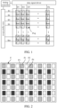
- FIG. 2 is a schematic diagram of a planar structure of a display substrate.
- the display substrate may include multiple pixel units P arranged in a matrix manner. At least one of the multiple pixel units P includes a first sub-pixel P1 emitting a first color light, a second sub-pixel P2 emitting a second color light, a third sub-pixel P3 emitting a third color light and a fourth sub-pixel P4 emitting a fourth color light.
- the four sub-pixels may each include a circuit unit and a light emitting device.
- the circuit unit may include a scan signal line, a data signal line and a pixel drive circuit. The pixel drive circuit is respectively connected to the scan signal line and the data signal line.
- the pixel drive circuit is configured to receive the data voltage transmitted by the data signal line and output a corresponding current to the light emitting device under the control of the scan signal line.
- the light emitting device in each sub-pixel is connected to a pixel drive circuit of a sub-pixel where the light emitting device is located, and is configured to emit light with a corresponding brightness in response to a current output by the pixel drive circuit of the sub-pixel where the light emitting device is located.
- the first sub-pixel P1 may be a red sub-pixel (R) emitting red light
- the second sub-pixel P2 may be a green sub-pixel (G) emitting green light
- the third sub-pixel P3 may be a white sub-pixel (W) emitting white light
- the fourth sub-pixel P4 may be a blue sub-pixel (B) emitting blue light.
- a sub-pixel may be a rectangle, a rhombus, a pentagon, or a hexagon.
- the four sub-pixels may be arranged in a horizontal side-by-side manner to form an RWBG pixel arrangement.
- the four sub-pixels may be arranged in a square, diamond, vertical side-by-side manner or the like, which is not limited here in the present disclosure.
- multiple sub-pixels sequentially arranged in the horizontal direction are referred to as a pixel row
- multiple sub-pixels sequentially arranged in the vertical direction are referred to as a pixel column.
- Multiple pixel rows and multiple pixel columns together form a pixel array.
- FIG. 3 is a schematic diagram of a sectional structure of a display substrate, and illustrates a structure of four sub-pixels of the display substrate.
- each sub-pixel of the display substrate may include a drive circuit layer 102 disposed on a base substrate 10, a light emitting structure layer 103 disposed at a side of the drive circuit layer 102 away from the base substrate, and an encapsulation layer 104 disposed at a side of the light emitting structure layer 103 away from the base substrate.
- the base substrate 10 may be a flexible base substrate, or a rigid base substrate.
- the drive circuit layer 102 of each sub-pixel may include a pixel drive circuit formed by multiple transistors and a storage capacitor.
- the light emitting structure layer 103 of each sub-pixel may include a light emitting device formed by multiple film layers.
- the multiple film layers may include an anode, a pixel definition layer, an organic light emitting layer, and a cathode.
- the anode is connected to a pixel drive circuit.
- the organic light emitting layer is connected to the anode.
- the cathode is connected to the organic light emitting layer.
- the organic light emitting layer emits light of a corresponding color under driving by the anode and the cathode.
- the encapsulation layer 104 may include a first encapsulation layer, a second encapsulation layer, and a third encapsulation layer that are stacked.
- the first encapsulation layer and the third encapsulation layer may be made of an inorganic material
- the second encapsulation layer may be made of an organic material
- the second encapsulation layer is disposed between the first encapsulation layer and the third encapsulation layer to ensure that external water vapor cannot enter the light emitting structure layer 103.
- the organic light emitting layer may include a Hole Injection Layer (HIL), a Hole Transport Layer (HTL), an Electron Block Layer (EBL), an Emitting Layer (EML), a Hole Block Layer (HBL), an Electron Transport Layer (ETL), and an Electron Injection Layer (EIL).
- HIL Hole Injection Layer
- HTL Hole Transport Layer
- EBL Electron Block Layer
- EML Emitting Layer
- HBL Hole Block Layer
- ETL Electron Transport Layer
- EIL Electron Injection Layer
- the hole injection layer, the hole transport layer, the electron block layer, the hole block layer, the electron transport layer and the electron injection layer of all sub-pixels may be connected together to form a common layer, and the emitting layers of all sub-pixels may be connected together to form a common layer, or may be isolated from each other, and the emitting layers of adjacent sub-pixels may overlap slightly.
- the display substrate may include other film layers, which are not limited here in the present disclosure.
- the pixel drive circuit may have a structure of 3T1C, 4T1C, 5T1C, 5T2C, 6T1C, 7T1C or 8T1C.
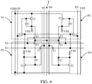
- FIG. 4 is a schematic diagram of an equivalent circuit of a pixel drive circuit. As shown in FIG. 4 , the pixel drive circuit has a structure of 3T1C, which may include three transistors (a first transistor T1, a second transistor T2, and a third transistor T3), one storage capacitor C, and six signal lines (a data signal line D, a first scan signal line G1, a second scan signal line G2, a compensation signal line S, a first power supply line VDD, and a second power supply line VSS).
- 3T1C which may include three transistors (a first transistor T1, a second transistor T2, and a third transistor T3), one storage capacitor C, and six signal lines (a data signal line D, a first scan signal line G1, a second scan signal line G2, a compensation signal line S, a first power supply line VDD
- the first transistor T1 is a switch transistor
- the second transistor T2 is a drive transistor
- the third transistor T3 is a compensation transistor.
- a first electrode of the storage capacitor C is coupled to a control electrode of the second transistor T2
- a second electrode of the storage capacitor C is coupled to a second electrode of the second transistor T2
- the storage capacitor C is configured to store a potential of the control electrode of the second transistor T2.
- a control electrode of the first transistor T1 is coupled to the first scan signal line G1, a first electrode of the first transistor T1 is coupled to the data signal line D, a second electrode of the first transistor T1 is coupled to the control electrode of the second transistor T2.
- the first transistor T1 is configured to receive a data signal transmitted by the data signal line D under control of the first scan signal line G1, so that the control electrode of the second transistor T2 receives the data signal.
- the control electrode of the second transistor T2 is coupled to a second electrode of the first transistor T1, a first electrode of the second transistor T2 is coupled to the first power supply line VDD, the second electrode of the second transistor T2 is coupled to a first electrode of a light emitting device, and the second transistor T2 is configured to generate a corresponding current at its second electrode under control of the data signal received by the control electrode of the second transistor.
- a control electrode of the third transistor T3 is coupled to the second scan signal line G2, a first electrode of the third transistor T3 is coupled to the compensation signal line S, a second electrode of the third transistor T3 is coupled to the second electrode of the second transistor T2.
- the third transistor T3 is configured to extract a threshold voltage Vth and a mobility of the second transistor T2 in response to compensation timing to compensate the threshold voltage Vth.
- the light emitting device may be an OLED, including a first electrode (anode), an organic emitting layer, and a second electrode (cathode) which are stacked.
- the first electrode of the OLED is coupled to the second electrode of the second transistor T2
- a second electrode of the OLED is coupled to the second power supply line VSS, and the OLED is configured to emit light with corresponding brightness in response to the current of the second electrode of the second transistor T2.
- a signal of the first power supply line VDD is a high-level signal continuously provided, and a signal of the second power supply line VSS is a low-level signal.
- the first transistor T1 to the third transistor T3 may be P-type transistors or may be N-type transistors. Use of a same type of transistors in a pixel drive circuit may simplify a process flow, reduce process difficulties of a display panel, and improve a product yield.
- low temperature poly silicon thin film transistors may be used, oxide thin film transistors may be used, or low temperature poly silicon thin film transistors and oxide thin film transistors may be used.
- An active layer of a low temperature poly silicon thin film transistor is made of Low Temperature Poly Silicon (LTPS for short), and an active layer of an oxide thin film transistor is made of an oxide.
- LTPS Low Temperature Poly Silicon
- the low temperature poly silicon thin film transistor has advantages of a high mobility, fast charging, and the like, and the oxide thin film transistor has advantages of a low leakage current and the like.
- a low temperature poly silicon thin film transistor and an oxide thin film transistor may be integrated on one display substrate to form a Low Temperature Polycrystalline Oxide (LTPO for short) display substrate, so that advantages of the two types of thin film transistors may be utilized, high Pixel Per Inch (PPI for short) and low-frequency drive may be achieved, power consumption may be reduced, and display quality may be improved.
- the light emitting device may be an organic light emitting diode (OLED), including a first electrode (anode), an organic light emitting layer, and a second electrode (cathode) that are stacked.
- an operation process of the pixel drive circuit illustrated in FIG. 4 may include: In a first stage A1, signals of the first scan signal line G1 and the second scan signal line G2 are high level signals, the data signal line D outputs a data voltage, the compensation signal line S outputs a compensation voltage, a signal of the first power supply line VDD is at a high level, and a signal of the second power supply line VSS is at a low level.
- a power supply voltage output from the first power supply line VDD provides a driving voltage to the first electrode of the OLED through the turned-on second transistor T2 to drive the OLED to emit light.
- the signals of the first scan signal line G1 and the second scan signal line G2 are low level signals, so that the first transistor T1 and the third transistor T3 are turned off, the voltage in the storage capacitor C still keeps the second transistor T2 in a turned-on state, the power supply voltage output by the first power supply line VDD continuously pulls up the potential of the second node N2, and the OLED continuously emits light.
- the potential of the second node N2 is equal to V data -V th , the second transistor T2 is turned off and the OLED no longer emits light.
- the OLED and the second transistor T2 are both forward biased.
- the power supply voltage output by the first power supply line VDD is greater than the data voltage output by the data signal line D
- the data voltage output by the data signal line D is greater than the compensation voltage output by the compensation signal line S
- the compensation voltage output by the compensation signal line S is greater than a power supply voltage output by the second power supply line VSS.
- Transparent display is an important personalized display field of the display technology, which refers to implement image display in a transparent state, in which a viewer can see not only images in a display device, but also scenes behind the display device, and Virtual Reality (VR) and Augmented Reality (AR) and 3D display functions can be implemented.
- each pixel is generally divided into a display area and a transparent area.
- the display area is provided with pixel drive circuits and light emitting elements for implementing image display, and the transparent area implements light transmission.
- An exemplary embodiment of the present disclosure provides a display substrate including a base substrate and multiple display units disposed on the base substrate. At least one display unit includes a display area and a transparent area, and at least one display area includes multiple sub-pixels.
- At least one display area is provided with a first power supply line and a second power supply line along a first direction.
- the first power supply line and the second power supply line extend in a second direction.
- At least one display area is provided with a first scan signal line, a second scan signal line, a second scan connection line and a first scan connection line in the second direction.
- the second scan connection line and the second scan signal line are connected to each other to form a first annular structure.
- the at least one display area is provided with a third scan connection line between the first scan signal line and the first scan connection line.
- the third scan connection line, the first scan connection line and the first scan signal line are connected to each other to form a second annular structure, and the first direction intersects with the second direction.
- the first scan signal line and the second scan signal line are respectively annularly wound with the corresponding scan connection lines in the display area, and the annular wound positions of the first scan signal line and the second scan signal line keep away from the first power supply line and the second power supply line. Therefore, a problem that a relatively large overlapped area between power supply lines and other signal lines leads to impact on the product yield is avoided. Under a functional condition where maintenance is available, the cross points between signal lines can be optimized to the minimum, thereby improving the product yield and providing technical support for transparent display products.
- FIG. 5 is a schematic diagram of a structure of a display panel according to an exemplary embodiment of the present disclosure, illustrating a structure of four sub-pixels (one pixel unit), and FIG. 6 is a schematic equivalent circuit diagram of the pixel drive circuits in the four sub-pixels shown in FIG. 5 .
- at least one pixel unit may include a first sub-pixel P1, a second sub-pixel P2, a third sub-pixel P3, and a fourth sub-pixel P4 arranged in sequence, and each sub-pixel includes a pixel drive circuit and a storage capacitor.
- the sub-pixels refer to regions in which the pixel drive circuits are provided.
- At least one pixel unit may further include one first scan signal line G1, one second scan signal line G2, one first power supply line VDD, one second power supply line VSS, four data signal lines D (in FIG. 6 , the four data signal lines D are a first data signal line D1 to a fourth data signal line D4, the first sub-pixel P1 is connected to the first data signal line D1, the second sub-pixel P2 is connected to the second data signal line D2, the third sub-pixel P3 is connected to the third data signal line D3, and the fourth sub-pixel P4 is connected to the fourth data signal line D4), one compensation signal line S, and four pixel drive circuits.
- the first scan signal line G1 and the second scan signal line G2 may extend along the first direction D1 and are sequentially arranged along the second direction D2, wherein the first direction D1 intersects with the second direction D2.
- the first power supply line VDD, the data signal lines D, and the compensation signal line S may extend along the second direction D2 and are correspondingly disposed along the first direction D 1.
- four data signal lines D and one compensation signal line S are disposed between the first power supply line VDD and the second power supply line VSS, two of the four data signal lines D are disposed between the compensation signal line S and the first power supply line VDD, and the other two of the four data signal line D are disposed between the compensation signal line S and the second power supply line VSS.
- four sub-pixels are formed between the first power supply line VDD and the second power supply line VSS by providing the four data signal lines D and the one compensation signal line S.
- four sub-pixels are also formed between two compensation signal lines S by providing one first power supply line VDD, one second power supply line VSS and four data signal lines D.
- one first power supply line VDD, two data signal lines D, one compensation signal line S, other two data signal lines D, and one first power supply line VSS may be arranged in sequence along the first direction D1.
- the first sub-pixel P1 and the second sub-pixel P2 are alternately arranged to form a first row
- the third sub-pixel P3 and the fourth sub-pixel P4 are alternately arranged to form a second row.
- the first sub-pixel P1 and the third sub-pixel P3 are alternately arranged to form a first column
- the second sub-pixel P2 and the fourth sub-pixel P4 are alternately arranged to form a second column.
- the pixel drive circuit in each sub-pixel may include a first transistor T1, a second transistor T2, a third transistor T3 and a storage capacitor.
- the first transistor T1 may include a first active layer, a first gate, a first source, and a first drain.
- the second transistor T2 may include a second active layer, a second gate, a second source, and a second drain.
- the third transistor T3 may include a third active layer, a third gate, a third source, and a third drain.
- the storage capacitor may include a first plate and a second plate.
- the first plate and the second plate are transparent conductive layers forming a transparent storage capacitor.
- the first scan signal line G1 is connected to a gate of the first transistor T1 in each sub-pixel
- the second scan signal line G2 is connected to a gate of the third transistor T3 in each sub-pixel.
- the data signal line D is connected to a first electrode of the first transistor T1 in each sub-pixel
- the compensation signal line S is connected to a first electrode of the third transistor T3 in each sub-pixel.
- the first power supply line VDD is connected to a first electrode of the second transistor T2 in each sub-pixel.
- a second electrode of the first transistor T1 in each sub-pixel is connected to a gate of the second transistor T2.
- a second electrode of the second transistor T2 in each sub-pixel is connected to the first electrode of the third transistor T3 and an anode of the light emitting device.
- the first plate in each sub-pixel is connected to the second electrode of the second transistor T2 and the second electrode of the third transistor T3 respectively, and the second plate in each sub-pixel is connected to the second electrode of the first transistor T1 and the gate of the second transistor T2, respectively.
- At least one pixel unit may include multiple connection lines, which at least include two transverse power supply connection lines extending along the first direction D 1 and two compensation connection lines extending along an opposite direction of the first direction D1, thereby forming a one-for-four structure of the first power supply line and a one-for-four structure of the compensation signal line.
- one transverse power supply connection line is disposed at the first sub-pixel P1 and the second sub-pixel P2.
- a first end of the transverse power supply connection line is connected to the first power supply line VDD through a via, and the other end of the transverse power supply connection line is connected to the second transistors T2 in the first sub-pixel P1 and the second sub-pixel P2 through vias.
- Another transverse power supply connection line is disposed at the third sub-pixel P3 and the fourth sub-pixel P4.
- One end of the transverse power supply connection line is connected to the first power supply line VDD through a via, and the other end of the transverse power supply connection line is connected to the second transistors T2 in the third sub-pixel P3 and the fourth sub-pixel P4 through vias.
- one first power supply line VDD can supply power signals to four sub-pixels.
- a compensation connection line is disposed in the middle of a pixel unit, the compensation connection line and the compensation signal line are connected to each other to form an integrated structure, and the compensation connection line is connected to the third transistor T3 in each sub-pixel through a via.
- one compensation signal line S can supply compensation signals to four sub-pixels.
- the quantity of signal lines is saved through the one-for-four structure of the first power supply line and the one-for-four structure of the compensation signal line, thereby reducing the space occupied, implementing a simple structure and a reasonable layout, making full use of the layout space, improving a space utilization rate, which is beneficial to improving a resolution.
- a drive circuit layer of a sub-pixel may include a first conductive layer, a first insulation layer, a semiconductor layer, a second insulation layer, a second conductive layer, a third insulation layer, a third conductive layer, a fourth insulation layer and a planarization layer which are stacked on the base substrate.
- the first conductive layer at least includes a first plate of a storage capacitor, a compensation signal line and a compensation connection line.
- the semiconductor layer at least includes active layers of three transistors.
- the second conductive layer at least includes a first scan signal line, a second scan signal line, a transverse power supply connection line, a second plate of the storage capacitor and gate electrodes of the three transistors.
- the third conductive layer at least includes a first power supply line VDD, a second power supply line VSS, a data signal line D and first electrodes and second electrodes of the three transistors. There is at least an overlapped area between an orthographic projection of the first plate on the base substrate and an orthographic projection of the second plate on the base substrate, thereby forming a storage capacitor.
- the second conductive layer may include a first scan connection line and a second scan connection line.
- the first scan connection line and the second scan connection line are located in the first sub-pixel P1 and the second sub-pixel P2, the first scan signal line and the second scan signal line are located in the third sub-pixel P3 and the fourth sub-pixel P4, and the second scan connection line and the second scan signal line are connected to each other to form an integrated structure.
- the third conductive layer may include a third scan connection line electrically connected to the first scan connection line and the first scan signal line through vias respectively.
- the second conductive layer may include a longitudinal power supply connection line and an auxiliary power supply line.
- the first power supply line VDD is electrically connected to the longitudinal power supply connection line through a via to form a double-layer first power supply trace
- the second power supply line VSS is electrically connected to the auxiliary power supply line through a via to form a double-layer second power supply trace.
- the third conductive layer may include an auxiliary cathode, and the auxiliary cathode and the second power supply line VSS are connected to each other to form an integrated structure.
- the sub-pixel in a direction perpendicular to the display substrate, the sub-pixel further includes a light emitting structure layer disposed at a side of the drive circuit layer away from the base substrate.
- the light emitting structure layer includes an anode, and an auxiliary connection electrode is disposed in a same layer as the anode.
- a "patterning process" mentioned in the present disclosure includes coating with a photoresist, mask exposure, development, etching, photoresist stripping, and other treatments for a metal material, an inorganic material, or a transparent conductive material, and includes coating with an organic material, mask exposure, development, and other treatments for an organic material.
- Deposition may be any one or more of sputtering, evaporation, and chemical vapor deposition.
- Coating may be any one or more of spray coating, spin coating, and ink-jet printing.
- Etching may be any one or more of dry etching and wet etching, which is not limited in present disclosure.
- a “thin film” refers to a layer of thin film made of a material on a base substrate through a process such as deposition, coating, etc. If the "thin film” does not need a patterning process in an entire preparation process, the “thin film” may also be called a “layer”. If the "thin film” needs a patterning process in an entire preparation process, it is called a “thin film” before the patterning process, and called a “layer” after the patterning process. The “layer” after the patterning process includes at least one "pattern”.
- a and B being disposed on a same layer means that A and B are formed simultaneously through a same patterning process, and a "thickness" of a film layer is a dimension of the film layer in a direction perpendicular to a display substrate.
- an orthographic projection of B is within a range of an orthographic projection of A
- an orthographic projection of A includes an orthographic projection of B refers to that a boundary of the orthographic projection of B falls within a range of a boundary of the orthographic projection of A, or the boundary of the orthographic projection of A coincides with the boundary of the orthographic projection of B.
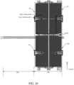
- FIGS. 7-26 are schematic diagrams of a manufacturing process of a display substrate according to the present disclosure, illustrating a layout structure of a display unit of a top-emission OLED display substrate, in which each display unit includes a display area 100 and a transparent area 200.
- the display area 100 includes a first sub-pixel P1, a second sub-pixel P2, a third sub-pixel P3 and a fourth sub-pixel P4.
- the pixel drive circuit of each sub-pixel includes a first transistor T1, a second transistor T2, a third transistor T3 and a storage capacitor.
- the manufacturing process of the display substrate may include following operations.
- the first plate 41 not only serves as a plate of the first capacitor and is configured to form the first capacitor with a second plate to be formed subsequently, the first plate 41 also serves as a shielding layer and is configured to shield light for the transistors to decrease an intensity of light irradiated onto the transistors and reduce the leakage current, thereby reducing an influence of light illuminance on the properties of the transistors.
- the compensation signal line S extends in the second direction D2, and a compensation connection line S-1 protruding in the first direction D1 and in the opposite direction of the first direction D1 is disposed on the compensation signal line S.
- the compensation connection line S-1 is connected to a first electrode of a third transistor to be formed subsequently for supplying a compensation signal to the third transistor in each sub-pixel.
- the first plate 41 is in a rectangular strip shape.
- the first plate 41 in the first sub-pixel P1 and the first plate 41 in the second sub-pixel P2 are each provided with a first opening 45 at a position close to the middle of the pixel unit and away from the compensation signal line S.
- the first plate 41 in the third sub-pixel P3 and the first plate 41 in the fourth sub-pixel P4 are each provided with a second opening 46 at a position close to the middle of the pixel unit and close to the compensation signal line S.
- the pattern of the first conductive layer in the first sub-pixel P1 and the pattern of the first conductive layer in the second sub-pixel P2 are mirror symmetrical with respect to a vertical axis (which may be the compensation signal line S), and the pattern of the first conductive layer in the third sub-pixel P3 and the pattern of the first conductive layer in the fourth sub-pixel P4 are mirror symmetrical with respect to the vertical axis.
- the pattern of the first conductive layer is formed in the display area 100, and there is no corresponding film layer in the transparent area 200.
- the semiconductor layer includes patterns of a first active layer 11, a second active layer 21 and a third active layer 31 which are arranged in each sub-pixel, as shown in FIGS. 9 and 10 , wherein FIG. 10 is a cross-sectional view taken along direction A-A in FIG. 9 .
- the first active layer 11 serves as an active layer of the first transistor
- the second active layer 21 serves as an active layer of the second transistor
- the third active layer 31 serves as an active layer of the third transistor.
- the first plate 41 serving as a shielding layer can shield a channel region of the second transistor to prevent the channel from being affected by the light, thereby preventing the channel from affecting the display effect due to generation of photo-generated leakage current.
- the first active layers 11 in the first sub-pixel P1 and the second sub-pixel P2 are disposed at positions close to the first openings 45, and the first active layers 11 in the third sub-pixel P3 and the fourth sub-pixel P4 are disposed at positions disposed close to the second openings 46.
- each third active layer 31 is disposed at a position close to the compensation connection line S-1, and there is an overlapped area between an orthographic projection of the third active layer 31 on the base substrate 10 and an orthographic projection of the compensation connection line S-1 on the base substrate 10.
- the third active layer 31 in the first sub-pixel P1 and the third active layer 31 in the third sub-pixel P3 are connected to each other to form an integrated structure
- the third active layer 31 in the second sub-pixel P2 and the third active layer 31 in the fourth sub-pixel P4 are connected to each other to form an integrated structure.
- the pattern of the semiconductor layer in the first sub-pixel P1 and the pattern of the semiconductor layer in the second sub-pixel P2 are mirror symmetric with respect to the vertical axis
- the pattern of the semiconductor layer in the third sub-pixel P3 and the pattern of the semiconductor layer in the fourth sub-pixel P4 are mirror symmetric with respect to the vertical axis.
- the semiconductor layer may be made of a metal oxide such as an oxide containing indium and tin, an oxide containing tungsten and indium, an oxide containing tungsten, indium and zinc, an oxide containing titanium and indium, an oxide containing titanium, indium and tin, an oxide containing indium and zinc, an oxide containing silicon, indium and tin, an oxide containing indium, gallium and zinc, etc.
- the semiconductor layer may be a single layer, two layers, or multiple layers.
- the pattern of the semiconductor layer is formed in the display area 100, and the transparent area 200 includes the base substrate 10 and the first insulation layer 61 arranged on the base substrate 10.
- Forming a pattern of a second conductive layer including: depositing a second insulation thin film and a second metal thin film sequentially on the base substrate on which the above patterns are formed, patterning the second insulation thin film and the second metal thin film by a patterning process to form a pattern of a second insulation layer 62 and a pattern of a second conductive layer disposed on the second insulation layer 62.
- the pattern of the second conductive layer includes a first scan signal line G1, a second scan signal line G2, a first scan connection line G1-1, a second scan connection line G2-1, a longitudinal power supply connection line 51, a transverse power supply connection line 52 and an auxiliary power supply line 53 which are formed in each display unit, and a second plate 42, a first gate 12, a second gate 22 and a third gate 32 which are formed in each sub-pixel, as shown in FIGS. 11 and 12 , wherein FIG. 12 is a cross-sectional view taken along direction A-A in FIG. 11 .
- the second plate 42 is in a rectangular strip shape.
- the second plates 42 in the first sub-pixel P1 and the second sub-pixel P2 are each provided with a third opening 47 at a position close to the middle of the pixel unit, the second plates 42 in the third sub-pixel P3 and the fourth sub-pixel P4 are each provided with a fourth opening 48 at a position close to the middle of the pixel unit, respectively.
- the first scan signal line G1 and the second scan signal line G2 each extend along the first direction D1
- the second scan connection line G2-1 has an inverted U-shaped structure.
- the second scan connection line G2-1 and the second scan signal line G2 are connected to each other to form an integrated structure.
- the first scan connection line G1-1 has a Chinese word "-"-shaped structure.
- the first scan connection line G1-1 and the second scan connection line G2-1 are located in the first sub-pixel P1 and the second sub-pixel P2, and the first scan signal line G1 and the second scan signal line G2 are located in the third sub-pixel P3 and the fourth sub-pixel P4.
- the overlapped area between the second scan signal line G2 and the third active layers 31 in the third sub-pixel P3 and the fourth sub-pixel P4 serves as gates 32 of the third transistors T3 in the third sub-pixel P3 and the fourth sub-pixel P4.
- the overlapped area between the second scan connection line G2-1 and the third active layers 31 in the first sub-pixel P1 and the second sub-pixel P2 serves as gates 32 of the third transistors T3 in the first sub-pixel P1 and the second sub-pixel P2.
- the first scan signal line G1 includes a "U"-shaped bent portion. There is an overlapped area between an orthographic projection of the first scan signal line G1 on the base substrate and an orthographic projection of the first active layers 11 in the third sub-pixel P3 and the fourth sub-pixel P4 on the base substrate.
- the overlapped area between the first scan signal line G1 and the first active layers 11 in the third sub-pixel P3 and the fourth sub-pixel P4 serves as gates 12 of the first transistors T1 in the third sub-pixel P3 and the fourth sub-pixel P4.
- the overlapped area between an orthographic projection of the first scan connection line G1-1 on the base substrate and an orthographic projection of the first active layers 11 in the first sub-pixel P1 and the second sub-pixel P2 on the base substrate is an overlapped area between an orthographic projection of the first scan connection line G1-1 on the base substrate and an orthographic projection of the first active layers 11 in the first sub-pixel P1 and the second sub-pixel P2 on the base substrate.
- the overlapped area between the first scan connection line G1-1 and the first active layers 11 in the first sub-pixel P1 and the second sub-pixel P2 serves as gates 12 of the first transistors T1 in the first sub-pixel P1 and the second sub-pixel P2.
- the second gate 22 is provided across the second active layer 21 and is connected with the second plate 42 to form an integrated structure.
- each display unit includes two longitudinal power supply connection lines 51 formed in the first sub-pixel P1 and the third sub-pixel P3, and the two longitudinal power supply connection lines 51 are each in a strip-shaped structure extending along the second direction D2.
- the longitudinal power supply connection line 51 is located at a side of the second plate 42 in the opposite direction of the first direction D 1.
- the longitudinal power supply connection line 51 is located at a side of the second plate 42 in the opposite direction of the first direction D1.
- the longitudinal power supply connection line 51 is configured to be connected to a first power supply line VDD to be formed subsequently to form a double-layer trace to ensure reliability of transmission of power supply signal and to reduce resistance of the first power supply line.
- two transverse power supply connection lines 52 are included in each display unit.
- One of the transverse power supply connection lines 52 is located at an upper side of the pixel unit (i.e. at a side of the first sub-pixel P1 and the second sub-pixel P2 away from the third sub-pixel P3 and the fourth sub-pixel P4), the other of the transverse power supply connection lines 52 is located at a lower side of the pixel unit (i.e. at a side of the third sub-pixel P3 and the fourth sub-pixel P4 away from the first sub-pixel P1 and the second sub-pixel P2).
- Each of the transverse power supply connection lines 52 may be provided with a through hole.
- the through hole is configured to reduce parasitic capacitance between the transverse power supply connection line 52 and the data signal line and the compensation signal line.
- the transverse power supply connection line 52 located at the upper side of the pixel unit may be connected with the longitudinal power supply connection line 51 located in the first sub-pixel P1 to form an integrated structure
- the transverse power supply connection line 52 located at the lower side of the pixel unit may be connected with the longitudinal power supply connection line 51 located in the third sub-pixel P3 to form an integrated structure.
- each display unit includes two auxiliary power supply lines 53, the two auxiliary power supply lines 53 are formed in the second sub-pixel P2 and the fourth sub-pixel P4 and are each in a strip-shaped structure extending along the second direction D2.
- the auxiliary power supply line 53 is located at a side of the second plate 42 in the first direction D1.
- the auxiliary power supply line 53 is located at a side of the second plate 42 in the first direction D1.
- the auxiliary power supply line 53 is configured to be electrically connected to a second power supply line to be formed subsequently to form a double-layer trace to ensure reliability of transmission of power supply signal and to reduce resistance of the second power supply line.
- the pattern of the second insulation layer 62 may be the same as the pattern of the second conductive layer, i.e., the second insulation layer 62 is located below the second conductive layer (i.e., at a side of the second conductive layer close to the base substrate), and there is no second insulation layer 62 in an area other than the second conductive layer.
- the first gates 12, the second gates 22 and the third gates 32 in the first sub-pixel P1 and the second sub-pixel P2 are respectively mirror symmetric with respect to the vertical axis
- the first gates 12, the second gates 22 and the third gates 32 in the third sub-pixel P3 and the third sub-pixel P4 are respectively mirror symmetric with respect to the vertical axis.
- this process further includes a metallization process.
- Conduction treatment is to perform plasma treatment by using the first gates 12, the second gates 22 and the third gates 32 as a shield after the formation of the pattern of the second conductive layer.
- the semiconductor layer in an area shielded by the first gates 12, the second gates 22 and the third gates 32 (i.e., an area of the semiconductor layer overlapped with the first gates 12, the second gates 22 and the third gates) serves as channel regions of the transistors, and the semiconductor layer in an area not shielded by the second conductive layer is treated into a conductive layer to form conductive source and drain regions.
- the pattern of the second conductive layer is formed in the display area 100, and the transparent area 200 includes the base substrate 10, the first insulation layer 61 and the second insulation layer 62 stacked on the base substrate 10, and the first scan signal line G1 and second scan signal line G2 disposed on the second insulation layer 62.
- Forming a pattern of a third insulation layer including: depositing a third insulation thin film on the base substrate on which the above patterns are formed, patterning the third insulation thin film by a patterning process to form a pattern of a third insulation layer 63 covering the above structure.
- the third insulation layer 63 is provided with patterns of multiple vias, which include: a first via V1 and a second via V2 located on the two sides of the first gate 12, a third via V3 and a fourth via V4 located on the two sides of the second gate 22, a fifth via V5 and a sixth via V6 located on the two sides of the third gate 32, multiple seventh via V7 located at the position of the auxiliary power supply line 53, an eighth via V8 located in a position of the compensation connection line S-1, a ninth via V9 located in an overlapped area between the first drain 14 to be formed subsequent and the second plate 42, a tenth via V10 located on the first electrode plate 41 and overlapped with an opening area on the second electrode plate 42, multiple eleventh vias V11 located at a position of the longitudinal power supply connection line 51, a thirteenth via V13 located at a position of the transverse power supply connection line 52, a fourteenth via V14 located at a position of the first scan connection line G1-1, and a fifteenth via V15 located
- the third insulation layer 63 in the first via V1 and the second via V2 is etched away to expose surfaces at both ends of the first active layer 11.
- the third insulation layer 63 in the third via V3 and the fourth via V4 is etched away to expose surfaces at both ends of the second active layer 21.
- the third insulation layer 63 in the fifth via V5 and the sixth via V6 is etched away to expose surfaces at both ends of the third active layer 31.
- the seventh vias V7 are located at the position of the auxiliary power supply line 53, the multiple seventh vias V7 are arranged at intervals, and the third insulation layer 63 in the seventh vias V7 is etched away to expose a surface of the auxiliary power supply line 53.
- the eighth via V8 is located at a position where the third source 33 to be formed subsequently is overlapped with the compensation connection line S-1, and the first insulation layer 61 and the third insulation layer 63 in the eighth via V8 are etched away to expose a surface of the compensation connection line S-1.
- the ninth via V9 is formed on the second plate 42, and the third insulation layer 63 in the ninth via V9 is etched away to expose a surface of the second plate 42.
- the tenth vias V10 in the first sub-pixel P1 and the second sub-pixel P2 are located in positions of the third openings 47 of the second plate 42, the tenth vias V10 in the third sub-pixel P3 and the fourth sub-pixel P4 are each located at a position of the fourth opening 48 of the second plate 42, and the first insulation layer 61 and the third insulation layer 63 in the tenth via V10 are etched away to expose a surface of the first plate 41.
- the eleventh vias V11 is located at a position of the longitudinal power supply connection line 51, the multiple eleventh vias V11 are arranged at intervals, and the third insulation layer 63 in the eleventh vias V11 is etched away to expose a surface of the longitudinal power supply connection line 51.
- the thirteenth via V13 is located at a position of an overlapped area between the transverse power supply connection line 52 and the second source 23 to be formed subsequently, and the third insulation layer 63 in the thirteenth via V13 is etched away to expose a surface of the transverse power supply connection line 52.
- the fourteenth via V14 is located at a position of an overlapped area between the first scan connection line G1-1 and the third scan connection line 54 to be formed subsequently, and the third insulation layer 63 in the fourteenth via V14 is etched away to expose a surface of the first scan connection line G1-1.
- the fifteenth via V15 is located at a position of the overlapped area between the first scan signal line G1 and the third scan connection line 54 to be formed subsequently, and the third insulation layer 63 in the fifteenth via V15 is etched away to expose a surface of the first scan signal line G1.
- the transparent area 200 includes a first insulation layer 61 and a second insulation layer 62 stacked on the base substrate 10, a first scan signal line G1 and a second scan signal line G2 disposed on the second insulation layer 62, and a third insulation layer 63 covering the first scan signal line G1 and the second scan signal line G2.
- the third conductive layer includes: one first power supply line VDD, one second power supply line VSS, four data signal lines D and two third scan connection lines 54 formed in each display unit, and patterns of a first source 13, a first drain 14, a second source 23, a second drain 24, a third source 33, a third drain 34 and a third plate 43 formed in each sub-pixel, as shown in FIGS. 15 and 16 , wherein FIG. 16 is cross-sectional view taken along direction A-A in FIG. 15 .
- the first power supply line VDD, the second power supply line VSS, the compensation signal line S and the data signal line D are arranged in parallel and all extend along the second direction D2.
- the second power line VSS is disposed within the second sub-pixel P2 and the fourth sub-pixel P4
- the first power supply line VDD is disposed within the first sub-pixel P1 and the third sub-pixel P3
- the compensation signal line S is disposed between the first power supply line VDD and the second power supply line VSS
- two of the data signal lines D are disposed between the second power supply line VSS and the compensation signal line S
- the other two of the data signal lines D are disposed between the first power supply line VDD and the compensation signal line S.
- the first power supply line VDD is connected to the longitudinal power supply connection line 51 and the transverse power supply connection line 52 through multiple eleventh vias V11, the transverse power supply connection line 52 is connected to the second source 23 of each sub-pixel through a thirteenth via V13, the second source 23 is connected to one end of the second active layer 21 through the third via V3, thereby realizing the connection between the second source 23 and the first power supply line VDD.
- the first power supply line VDD and the longitudinal power supply connection line 51 form a double-layer trace, thereby ensuring the reliability of transmission of power supply signal and reducing the resistance of the first power supply line VDD.
- the second power supply line VSS is connected to the auxiliary power supply line 53 through multiple seventh vias V7, so that the second power supply line VSS and the auxiliary power supply line 53 form a double-layer trace, thereby ensuring the reliability of transmission of power supply signal and reducing the resistance of the second power supply line VSS.
- widths of the first power supply line VDD and the second power supply line VSS along the first direction D1 are both greater than a width of the compensation signal line S along the first direction D1
- widths of the first power supply line VDD and the second power supply line VSS along the first direction D 1 are both greater than a width of a data signal line D along the first direction D1, such that the resistances of the first power supply line VDD and the second power supply line VSS can be further reduced.
- the compensation connection line S-1 is connected to the third source 33 of each sub-pixel through the eighth via V8. Since the compensation connection line S-1 is disposed in the middle of the upper sub-pixels and the lower sub-pixels of the display area 100, the compensation signal line S is disposed in the middle of the left sub-pixels and the right sub-pixels of the display area 100, the compensation connecting line S-1 and the compensation signal line S are connected to each other to form an integrated structure, the third transistors of the left sub-pixels and the right sub-pixels are symmetrically arranged with respect to the compensation signal line S, and such symmetrical design makes each display unit only need to use one compensation signal line S, which can ensure that the RC delay of the compensation signal before writing into the transistor is basically the same, and ensure the display uniformity.
- the third scan connection line 54 is a straight line or a broken line structure extending in the second direction D2, and the third scan connection line 54 is connected to the first scan connection line G1-1 through the fourteenth via V14, and the third scan connection line 54 is connected to the first scan signal line G1 through the fifteenth via V15.
- the data signal line D of the first sub-pixel P1 is disposed at a side of the first sub-pixel P1 close to the first power supply line VDD
- the data signal line D of the second sub-pixel P2 is disposed at a side of the second sub-pixel P2 close to the second power supply line VSS
- the data signal line D of the third sub-pixel P3 is disposed at a side of the third sub-pixel P3 close to the compensation signal line S
- the data signal line D of the fourth sub-pixel P4 is disposed at a side of the fourth sub-pixel P4 close to the compensation signal line S.
- the first source 13 is connected to a data signal line D to formed an integrated structure with the data signal line, so that each data signal line D is connected to the first source 13 of the sub-pixel in which the data signal line is located.
- the first source 13 is connected to one end of the first active layer 11 through the first via V1, the first drain 14 is connected to the other end of the first active layer 11 through the second via V2, and the first drain 14 is connected to the second gate 22 and the second plate 42 through the ninth via V9, thus enabling the first drain 14, the second gate 22 and the second plate 42 to have a same potential.
- the second source 23 is connected to one end of the second active layer 21 through the third via V3, the second source 23 is connected to the first power supply line VDD through the thirteenth via V13, and the transverse power supply line 52 is connected to the first power supply line VDD through the eleventh via V11, thereby realizing the connection between the second source 23 and the first power supply line VDD.
- the second drain 24 is connected to the other end of the second active layer 21 through the fourth via V4, the third source 33 is connected to one end of the third active layer 31 through the fifth via V5 and also connected to the compensation connection line S-1 through the eighth via V8, the compensation connection line S-1 and the compensation signal line S are connected to each other to form an integrated structure, thereby realizing the connection between the third source 33 and the compensation signal line S.
- the third drain 34 is connected to the other end of the third active layer 31 through the sixth via V6.
- the second drain 24, the third drain 34 and the third plate 43 are connected to each other to form an integrated structure, and the third plate 43 is connected to the first plate 41 through the tenth via V10. Therefore, the second drain 24 is respectively connected to the first plate 41 and the third plate 43, and the third drain 34 is respectively connected to the first plate 41 and the third plate 43, such that the second drain 24, the third drain 34, the first plate 41 and the third plate 43 to have a same potential.
- the first sources 13, the first drains 14, the second sources 23, the second drains 24, the third sources 33, the third drains 34 and the third plates 43 in the first sub-pixel P1 and the second sub-pixel P2 are respectively mirror symmetric with respect to the vertical axis.
- the first sources 13, the first drains 14, the second sources 23, the second drains 24, the third sources 33, the third drains 34 and the third plates 43 in the third sub-pixel P3 and the fourth sub-pixel P4 are mirror symmetric with respect to the vertical axis.
- the pattern of the third conductive layer is formed in the display area 100, and the transparent area 200 includes the first insulation layer 61 and the second insulation layer 62 stacked on the base substrate 10, the first scan signal line G1 and the second scan signal line G2 disposed on the second insulation layer 62, and the third insulation layer 63 covering the first scan signal line G1 and the second scan signal line G2.
- Forming patterns of a fourth insulation layer and a planarization layer including: first depositing a fourth insulation thin film on the base substrate on which the above patterns are formed, then coating a planarization thin film, and etching the fourth insulation thin film through masking, exposure and development of the planarization thin film to form a pattern of a fourth insulation layer 64 covering the above structures and a pattern of a planarization layer (PLN) 65 arranged on the fourth insulation layer 64.
- the fourth insulation layer 64 and the planarization layer 65 are provided with patterns of multiple vias, which at least include: a sixteenth via V16 located at the position of the third plate 43 in each sub-pixel of the display area 100 and a seventeenth via V17 on the second power supply line VSS, as shown in FIGS. 17 and 18 , wherein FIG. 18 is a cross-sectional view taken along direction A-A in FIG. 17 .
- the sixteenth via V16 is located in the middle of the third plate 43, the fourth insulation layer 64 and the planarization layer 65 in the sixteenth via V16 are etched away to expose a surface of the third plate 43, and the fourth insulation layer 64 and the planarization layer 65 in the seventeenth via V17 are etched away to expose a surface of the second power supply line VSS.
- the transparent area 200 includes the first insulation layer 61 and the second insulation layer 62 stacked on the base substrate 10, the first scan signal line G1, the second scan signal line G2 disposed on the second insulation layer 62, the third insulation layer 63 covering the first scan signal line G1 and the second scan signal line G2, and the fourth insulation layer 64 and the planarization layer 65 disposed on the third insulation layer 63.
- Forming a pattern of a first transparent conductive layer including: depositing a first transparent conductive thin film on the base substrate on which the above patterns are formed, patterning the first transparent conductive thin film by a patterning process to form a pattern of a first transparent conductive layer on the planarization layer 65.
- the first transparent conductive layer includes a first anode 70 and a first connection electrode 81.
- the first anode 70 is formed in each sub-pixel of the display area 100, the first anode 70 in each sub-pixel is connected to the drain of the second transistor T2 through the sixteenth via V16 in the corresponding sub-pixel.
- the first connection electrode 81 is formed at the position of the seventeenth via V17 on the second power supply line VSS in the display area 100, and first connection electrode 81 is connected to the second power supply line VSS through the seventeenth via V17, as shown in FIGS. 19 and 20 , wherein FIG. 20 is a cross-sectional view taken along direction A-A in FIG. 19 .
- the drain of the second transistor T2, the drain of the third transistor T3 and the third plate 43 in each sub-pixel are connected to each other to form an integrated structure, such that the first anode 70 is connected to the drain of the second transistor T2 in each sub-pixel.
- the four first anodes 70 may form a red light emitting unit, a green light emitting unit, a blue light emitting unit and a white light emitting unit.
- the first anode 70 may include two sub-anode blocks disposed separately and a connection structure connected to the two sub-anodes respectively, and the two sub-anodes are connected to each other through the connection structure.
- the connection structure may include a first connection electrode 701 having a U-shaped structure and a second connection electrode 702. Two ends of the first connection electrode 701 are respectively connected to one of the two sub-anode blocks. One end of the second connection electrode 702 is connected to a drive transistor, and the other end of the second connection electrode 702 is connected to the first connection electrode 701, so that the two sub-anode blocks are connected to each other through the connection structure.
- connection electrode 701 in the connection structure may be laser cut, whereby one of the two sub-anode blocks from one sub-pixel may be electrically connected to the drive transistor, and the other sub-anode block is floated, such that the sub-pixel may be normally driven.
- the four first anodes 70 are arranged in a square.
- the upper left first anode 70 is connected to the third plate 43 of the first sub-pixel P1 through the sixteenth via V16 of the first sub-pixel P1
- the upper right first anode 70 is connected to the third plate 43 of the second sub-pixel P2 through the sixteenth via V16 of the second sub-pixel P2
- the lower left first anode 70 is connected to the third plate 43 of the third sub-pixel P3 through the sixteenth via V16 of the third sub-pixel P3
- the lower right first anode 70 is connected to the third plate 43 of the fourth sub-pixel P4 through the sixteenth via V16 of the fourth sub-pixel P4.
- the arrangement of the first anodes 70 in the display area 100 may be adjusted according to actual needs, which is not limited herein in the present disclosure.
- the transparent area 200 includes the first insulation layer 61 and the second insulation layer 62 stacked on the base substrate 10, the first scan signal line G1 and the second scan signal line G2 disposed on the second insulation layer 62, the third insulation layer 63 covering the first scan signal line G1 and the second scan signal line G2, and the fourth insulation layer 64 and the planarization layer 65 disposed on the third insulation layer 63.
- Forming a pattern of an anode may include: sequentially depositing a fourth metal thin film and a second transparent conductive thin film on the base substrate on which the foregoing patterns are formed, and patterning the fourth metal thin film and the second transparent conductive thin film by a patterning process to form patterns of a second anode 71, a third anode 72, a second connection electrode 82 and a third connection electrode 83.
- the second anode 71 is disposed at a side of the first anode 70 away from the base substrate and is connected to the first anode 70.
- the third anode 72 is disposed at a side of the second anode 71 away from the base substrate and is connected to the second anode 71.
- the second connection electrode 82 is disposed at a side of the first connection electrode 81 away from the base substrate and is connected to the first connection electrode 81.
- the third connection electrode 83 is disposed at a side of the second connection electrode 82 away from the base substrate and is connected to the second connection electrode 82.
- the first anode 70, the second anode 71, and the third anode 72 are stacked to form an anode 74.
- the first connection electrode 81, the second connection electrode 82, and the third connection electrode 83 are stacked to form an auxiliary connection electrode, as shown in FIGS. 21 and 22 , wherein FIG. 22 is a cross-sectional view taken along direction A-A in FIG. 21 .
- shapes of the second anode 71 and the third anode 72 are similar to a shape of the first anode 70, an orthographic projection of the second anode 71 on the base substrate may be within a range of an orthographic projection of the first anode 70 on the base substrate, and the orthographic projection of the second anode 71 on the base substrate may be within a range of an orthographic projection of the third anode 72 on the base substrate.
- shapes of the second connection electrode 82 and the third connection electrode 83 are similar to a shape of the first connection electrode 81, an orthographic projection of the second connection electrode 82 on the base substrate may be within a range of an orthographic projection of the first connection electrode 81 on the base substrate, and the orthographic projection of the second connection electrode 82 on the base substrate may be within a range of an orthographic projection of the third connection electrode 83 on the base substrate.
- the first connection electrode 81 located at a side (lower side) of the second connection electrode 82 close to the base substrate has an edge protruding from a contour of the second connection electrode 82, forming a "roof seat” structure
- the third connection electrode 83 located at a side (upper side) of the second connection electrode 82 away from the base substrate has an edge protruding from the contour of the second connection electrode 82
- the first connection electrode 81 and the third connection electrode 83 form an "eave" structure, so that the stacked first connection electrode 81, the second connection electrode 82 and the third connection electrode 83 form a structure with a shape like a letter "I".
- the first anode 70 located at a side (lower side) of the second anode 71 close to the base substrate has an edge protruding from a contour of the second anode 71, forming a "roof seat” structure
- the third anode 72 located at a side (upper side) of the second anode 71 away from the base substrate has an edge protruding from a contour of the second anode 71, forming an "eave” structure, so that the stacked first anode 70, second anode 71 and third anode 72 form a structure with a shape like a letter "I".
- a first etchant and a second etchant may be used for etching respectively, and a structure, with a shape like a letter "I", of the auxiliary electrode and the anode can be formed by drilling.
- the first etchant may be an etchant (ITO etchant) for etching a transparent conducting material
- the second etchant may be an etchant (metal etchant) for etching a metal material.
- the etching process may include: firstly etching the second transparent conductive thin film which is not covered by the photoresist by using the ITO etchant, so that an area not covered by the photoresist exposes the fourth metal thin film, to form patterns of the third anode 72 and the third connection electrode 83. Then, the exposed fourth metal thin film is etched using the metal etchant to form patterns of the second anode 71 and the second connection electrode 82.
- a material of the fourth metal film may include any one or more of silver (Ag), copper (Cu), aluminum (Al), titanium (TI), and molybdenum (Mo), or an alloy material of the above metals, and a second transparent conductive material may be indium tin oxide (ITO) or indium zinc oxide (IZO), etc.
- Forming a pattern of a pixel definition layer may include: coating a pixel definition thin film on the base substrate on which the above patterns are formed, and patterning the pixel definition thin film by a patterning process to form the pattern of the pixel definition layer (PDL) 91.
- the pixel definition layer 91 is provided with a first pixel opening K1 and a second auxiliary electrode opening K2.
- the pixel definition layer 91 in the first pixel opening K1 is removed to expose part of a surface of the third anode 72 in the anode, and the pixel definition layer 91 in the second auxiliary electrode opening K2 is removed to expose entire surfaces of the second connection electrode 82 and the third connection electrode 83 in the auxiliary connection electrode, as illustrated in FIGS. 23 and 24 , wherein FIG. 24 is a cross-sectional view taken along direction A-A in FIG. 23 .
- an orthographic projection of the first pixel opening K1 on the base substrate is within a range of the orthographic projection of the third anode 72 on the base substrate
- an orthographic projection of the second auxiliary electrode opening K2 on the base substrate is within a range of the orthographic projection of the first connection electrode 81 on the base substrate
- the orthographic projections of the second connection electrode 82 and the third connection electrode 83 on the base substrate are within the range of the orthographic projection of the second auxiliary electrode opening K2 on the base substrate.
- the second auxiliary electrode opening K2 exposing entire surfaces of the second connection electrode 82 and the third connection electrode 83 means that the second auxiliary electrode opening has a second lower opening close to the base substrate and a second upper opening away from the base substrate, the orthographic projections of the second connection electrode 82 and the third connection electrode 83 on the base substrate are within a range of an orthographic projection of the second lower opening on the base substrate.
- the pixel definition layer may be made of polyimide, acrylic, polyethylene terephthalate, or the like.
- a shape of the first pixel opening K1 may be similar to a shape of multiple anode blocks, and a shape of the second auxiliary electrode opening K2 may be a rectangle.
- cross-sectional shapes of the first pixel opening K1 and the second auxiliary electrode opening K2 may be a rectangle or a trapezoid.
- Forming a pattern of an organic emitting layer may include: evaporating an organic light emitting material on the base substrate on which the above patterns are formed to form patterns of an organic light emitting layer 92 and an organic light emitting block.
- the organic light emitting layer 92 is disposed in a region outside the third connection electrode 83, the organic light emitting layer 92 is connected to the third anode 72 in the anode 74 through the first pixel opening K1, the organic light emitting block is disposed on a surface of the third connection electrode 83 away from the base substrate, and the organic light emitting block is disposed to be isolated from the organic light emitting layer 92, as illustrated in FIG. 25 .
- the pattern of the organic light emitting layer may also be formed by ink jet printing, which is not limited in the embodiments of the present disclosure.
- the third connection electrode 83 protrudes from the second connection electrode 82 by a certain distance, so the organic light emitting material is broken at a side edge of the third connection electrode 83, the organic light emitting blockis formed on a second upper surface of the third connection electrode 83, and the organic light emitting layer 92 is formed in the region outside the third connection electrode 83, thus achieving the mutual isolation between the organic light emitting layer 92 and the organic light emitting block.
- an orthographic projection of the organic light emitting block on the base substrate may be approximately equal to an orthographic projection of the third connection electrode on the base substrate.
- the organic light emitting layer is separated by the auxiliary electrode of a structure with a shape like a letter "I" to form an isolated and separated organic light emitting block, which effectively avoids the interference of the organic light emitting block with emitted light, thereby improving the quality of the emitted light and facilitating improvement of the display quality.
- the organic light emitting layer may include an emitting layer (EML) and any one or more of the following layers: a Hole Injection Layer (HIL), a Hole Transport Layer (HTL), an Electron Block Layer (EBL), a Hole Block Layer (HBL), an Electron Transport Layer (ETL), and an Electron Injection Layer (EIL).
- EML Electron Injection Layer
- the organic light emitting layer may be formed by evaporation using a Fine Metal Mask (FMM) or an open mask, or by an inkjet process.
- FMM Fine Metal Mask
- the organic emitting layer may be manufactured through a following manufacturing method. First, a hole injection layer and a hole transport layer are sequentially evaporated by using an open mask, and a common layer of the hole injection layer and the hole transport layer is formed on the display substrate. Then, by using a fine metal mask, an electron block layer and a red emitting layer are evaporated in a red sub-pixel, an electron block layer and a green emitting layer are evaporated in a green sub-pixel, and an electron block layer and a blue emitting layer are evaporated in a blue sub-pixel.
- Electron block layers and emitting layers of adjacent sub-pixels may be overlapped slightly (for example, an overlapping portion accounts for less than 10% of an area of a pattern of a respective emitting layer), or may be isolated. Then, a hole block layer, an electron transport layer, and an electron injection layer are sequentially evaporated by using an open mask, and a common layer of the hole block layer, the electron transport layer, and the electron injection layer is formed on the display substrate.
- an electron block layer may be used as a micro-cavity adjustment layer of a light emitting device.
- a thickness of an electron block layer By designing a thickness of an electron block layer, a thickness of the organic emitting layer between the cathode and the anode may satisfy a design for a length of a micro-cavity.
- the hole transport layer, the hole block layer, or the electron transport layer in the organic emitting layer may be used as a micro-cavity adjustment layer of a light emitting device, which is not limited in the present disclosure.
- an emitting layer may include a host material and a dopant material doped into the host material.
- a doping ratio of the dopant material of the emitting layer is 1% to 20%.
- the host material of the emitting layer may effectively transfer exciton energy to the dopant material of the emitting layer to excite the dopant material of the emitting layer to emit light.
- the host material of the emitting layer "dilutes" the dopant material of the emitting layer, thus effectively improving fluorescence quenching caused by collisions between molecules of the dopant material of the emitting layer and collisions between energies, and improving a luminous efficiency and device life.
- the doping ratio refers to a ratio of a mass of the dopant material to a mass of the emitting layer, that is, a mass percentage.
- the host material and the dopant material may be co-evaporated through a multi-source evaporation process, so that the host material and the dopant material are uniformly dispersed in the emitting layer.
- a doping ratio may be adjusted by controlling an evaporation rate of the dopant material or by controlling an evaporation rate ratio of the host material to the dopant material during an evaporation process.
- a thickness of the emitting layer may be about 10 nm to 50 nm.
- the hole injection layer may be made of an inorganic oxide, such as molybdenum oxide, titanium oxide, vanadium oxide, rhenium oxide, ruthenium oxide, chromium oxide, zirconium oxide, hafnium oxide, tantalum oxide, silver oxide, tungsten oxide, or manganese oxide, or may be made of a p-type dopant of a strongly electron withdrawing system and a dopant of a hole transport material.
- a thickness of the hole injection layer may be about 5 nm to 20 nm.
- the hole transport layer may be made of a material with a relatively high hole mobility, such as an aromatic amine compound, and its substituent group may be carbazole, methylfluorene, spirofluorene, dibenzothiophene, or furan.
- a thickness of the hole transport layer may be about 40 nm to 150 nm.
- the hole block layer and the electron transport layer may be made of aromatic heterocyclic compounds, such as benzimidazole derivatives, imidazopyridine derivatives, benzimidazophenanthridine derivatives, and other imidazole derivatives; pyrimidine derivatives, triazine derivatives, and other azine derivatives; quinoline derivatives, isoquinoline derivatives, phenanthroline derivatives, and other compounds containing a nitrogen-containing six-membered annular structure (also including compounds having a phosphine oxide-based substituent on a heterocyclic ring) .
- a thickness of the hole block layer may be about 5 nm to 15 nm
- a thickness of the electron transport layer may be about 20 nm to 50 nm.
- an electron injection layer may be made of an alkali metal or a metal, such as lithium fluoride (LiF), ytterbium (Yb), magnesium (Mg), or Calcium (Ca), or a compound of these alkali metals or metals.
- a thickness of the electron injection layer may be about 0.5 nm to 2 nm.
- Forming a pattern of a cathode may include: evaporating a cathode material on the base substrate on which aforementioned patterns are formed to form a pattern of a cathode 94.
- the cathode 94 is connected to the organic light emitting layer 92, as shown in FIG. 26 .
- the cathode 94 may be in an integrated structure. In a region outside the auxiliary connection electrode, the cathode 94 is disposed on the organic light emitting layer 92. In a region where the auxiliary connection electrode is located, the cathode 94 is disposed on an exposed surface of the organic light emitting block on the one hand, and on an exposed surface of the auxiliary connection electrode on the other hand, thus forming a structure wrapping the auxiliary connection electrode and the organic light emitting block.
- the light emitting structure layer includes the anode, the auxiliary connection electrode, the pixel definition layer, the organic light emitting layer and the cathode.
- the organic light emitting layer is respectively connected to the anode and the cathode, the cathode is connected to the auxiliary connection electrode, and the auxiliary connection electrode is electrically connected to the second power supply line through the auxiliary cathode.
- the manufacturing process of the display substrate may further include forming a pattern of an encapsulation layer, and forming the pattern of the encapsulation layer may include: firstly, using an open mask plate to deposit a first inorganic thin film by means of plasma enhanced chemical vapor deposition (PECVD) to form the first encapsulation layer.
- PECVD plasma enhanced chemical vapor deposition
- ink-jet printing is performed on an organic material on the first encapsulation layer through an ink-jet printing process, and a second encapsulation layer is formed after curing, and then depositing a second inorganic thin film by using an open mask to form a third encapsulation layer, wherein the first encapsulation layer, the second encapsulation layer and the third encapsulation layer form the encapsulation layer.
- the first encapsulation layer and the third encapsulation layer may be made of any one or more of silicon oxide (SiOx), silicon nitride (SiNx), silicon carbide (SiC), silicon carbonitride (SiCN) and silicon nitride (SiON), and each may be in a single-layer structure, a multi-layer structure, or a composite layer structure.
- the second encapsulation layer may be made of a resin material, thereby forming a stacked structure of inorganic material/organic material/inorganic material, wherein the organic material layer is disposed between the two inorganic material layers, thus ensuring that the external moisture cannot enter the light emitting structure layer.
- a color film layer and a black matrix may be made on another substrate by a patterning process.
- a color film cover plate is formed, a frame sealing glue is coated on a surface of the color film cover plate, and the color film cover plate and the display substrate describe above are pressed together to form an OLED display panel as shown in FIG. 5 .
- FIG. 5 only the black matrix BM is shown, and the color film layer is not shown.
- the black matrix has multiple opening areas arranged in a matrix, and the color film layer is filled in the opening areas.
- the color film layer and the black matrix may also be manufactured on the display substrate.
- the color film layer and the black matrix may be manufactured after the formation of the cathode and before the formation of the encapsulation layer.
- the first active layer 11, the first gate 12, the first source 13 and the first drain 14 constitute the first transistor T1.
- the second active layer 21, the second gate 22, the second source 23 and the second drain 24 constitute the second transistor T2.
- the third active layer 31, the third gate 32, the third source 33 and the third drain 34 constitute the third transistor T3.
- the first plate 41 and the second plate 42 constitute the first capacitor.
- the second plate 42 and the third plate 43 constitute the second capacitor.
- the first capacitor and the second capacitor are in a parallel structure, implementing storage of the potential of the second gate 22 of the sub-pixel in which the first capacitor and the second capacitor are located.
- the first transistors T1, the second transistors T2, the third transistors T3, the first capacitors and the second capacitors in the first sub-pixel P1 and the second sub-pixel P2 are mirror symmetric with respect to the compensation signal line S
- the first transistors T1, the second transistors T2, the third transistors T3, the first capacitors and the second capacitors in the third sub-pixel P3 and the fourth sub-pixel P4 are mirror symmetric with respect to the compensation signal line S.
- the first gate 12 is connected to the first scan signal line G1
- the first source 13 is connected to the data signal line D
- the first drain 14 is connected to the second gate 22 of the sub-pixel where the first drain 14 is located.
- the second gate 22 is connected to the first drain 14 of the sub-pixel where the second gate 22 is located, the second source 23 is connected to the first power supply line VDD through the power connection line 52, and the second drain 24 is connected to the anode of the sub-pixel where the second drain 24 is located.
- the third gate 32 is connected to the second scan signal line G2, the third source 33 is connected to the compensation signal line S, and the third drain 34 is connected to the second drain 24 of the sub-pixel where the third drain 34 is located.
- the first plate 41 is connected to the second drain 24 and the third drain 34 of the sub-pixel where the first plate 41 is located
- the second plate 42 is connected to the second gate 22 and the first drain 14 of the sub-pixel where the second plate 42 is located
- the third plate 43 is connected to the second drain 24 and the third drain 34 of the sub-pixel where the third plate 43 is located.
- the anode 74 is connected to the second drain 24 of the sub-pixel where the anode 74 is located, and the cathode 94 covering all sub-pixels is connected to the second power supply line VSS through the auxiliary connection electrode, so that the organic light emitting layer 92 between the anode 70 and the cathode 94 emits light with corresponding brightness in response to a current of the second drain 24 of the sub-pixel where the organic light emitting layer 92 is located.
- the first conductive layer, the second conductive layer, and the third conductive layer may be made of a metal material, for example, any one or more of Argentum (Ag), Copper (Cu), Aluminum (Al), and Molybdenum (Mo), or an alloy material of the above-mentioned metals, for example, an Aluminum-Neodymium alloy (AINd) or a Molybdenum-Niobium alloy (MoNb), and may be in a single-layer structure, or in a multilayer composite structure such as Mo/Cu/Mo, etc.
- AINd Aluminum-Neodymium alloy
- MoNb Molybdenum-Niobium alloy
- the first insulation layer, the second insulation layer, the third insulation layer, and the fourth insulation layer may be made of any one or more of silicon oxide (SiOx), silicon nitride (SiNx), and silicon oxynitride (SiON), and may be single-layer, multilayers, or composite layer.
- the first insulation layer is called a buffer layer, which is used for improving a capability of water and oxygen resistance of the base substrate
- the second insulation layer is called a gate insulation (GI) layer
- the third insulation layer is called an interlayer dielectric (ILD) layer
- the fourth insulation layer is called a passivation (PVX) layer.
- a thickness of the second insulation layer is smaller than a thickness of the third insulation layer, and a thickness of the first insulation layer is smaller than a sum of thicknesses of the second insulation layer and the third insulation layer, which increases the capacity of the storage capacitor, while ensuring the insulation effect.
- the planarization layer may be made of an organic material
- the transparent conductive thin film may be made of indium tin oxide (ITO) or indium zinc oxide (IZO)
- the pixel definition layer may be made of polyimide, acrylic or polyethylene terephthalate.
- the cathode may be made of any one or more of magnesium (Mg), silver (Ag), aluminum (Al), copper (Cu) and lithium (Li), or an alloy made of any one or more of the above metals.
- the first insulation layer has a thickness of 3000 angstroms to 5000 angstroms
- the second insulation layer has a thickness of 1000 angstroms to 2000 angstroms
- the third insulation layer has a thickness of 4500 angstroms to 7000 angstroms
- the fourth insulation layer has a thickness of 3000 angstroms to 5000 angstroms.
- the first conductive layer has a thickness of 80 angstroms to 1200 angstroms
- the second conductive layer has a thickness of 3000 angstroms to 5000 angstroms
- the third conductive layer has a thickness of 3000 angstroms to 9000 angstroms.
- the semiconductor layer may be made of an oxide containing indium and tin, an oxide containing tungsten and indium, an oxide containing tungsten, indium and zinc, an oxide containing titanium and indium, an oxide containing titanium, indium and tin, an oxide containing indium and zinc, an oxide containing silicon, indium and tin, an oxide containing indium, gallium and zinc, etc.
- the semiconductor layer may be a single layer, two layers, or multiple layers.
- a display substrate according to the present disclosure includes:
- the first scan connection line and/or the second scan connection line on two sides of the short-circuit fault point can be cut off by laser cutting to repair the short-circuit fault.
- the first scan connection line on two sides of the short-circuit fault point may be cut off by laser cutting to repair the short-circuit fault.
- a position of the first connection electrode in the connection structure at one side of the sub-anode block can be cut by laser, whereby another sub-anode block in the sub-pixel corresponding to the sub-anode block can be electrically connected to the drive transistor, and the sub-anode block is floated to repair the short circuit fault.
- the structure shown in the present disclosure and the manufacturing process thereof are merely an exemplary description.
- a corresponding structure may be altered and patterning processes may be increased or reduced according to actual needs.
- the display area may include 3 sub-pixels.
- the pixel drive circuit may be 5T1C or 7T1C.
- other electrodes or leads may further be provided in the film layer structure, which is not limited herein in the present disclosure.
- the first scan signal line and the second scan signal line are designed to be respectively annularly wound with corresponding scan connection lines in the display area, and the annular wound positions of the first scan signal line and the second scan signal line are kept away from the first power supply line and the second power supply line. Therefore, a problem that a relatively large overlapped area of power supply lines and other signal lines leads to impact on the product yield is avoided. Under a functional condition where maintenance is available, the cross points between signal lines can be optimized to the minimum, thereby improving the product yield and providing technical support for transparent display of products.
- the second plate of metal oxide material as a plate of the storage capacitor, the second plate forms storage capacitors with the first plate in the first conductive layer and the third plate in the third conductive layer, respectively.
- the first plate and the third plate have a same potential, and the second plate has a potential different from that of the first plate and the third plate, so that two parallel storage capacitors are formed among the first plate, the second plate and the third plate, which effectively increases the capacity of the storage capacitors and is beneficial to realizing high-resolution display.
- the manufacturing process according to the present disclosure may be implemented using the existing mature manufacturing equipment, and improvements to the existing process are small, such that it may be well compatible with the existing manufacturing process, be simple to implement, and be easy to practice, thereby achieving high production efficiency, low production cost and high yield rate.
- Internal repair of sub-pixel can be carried out through the design of the present disclosure, and the product yield is increased by more than twice.
- the display substrate of the present disclosure may be applied to a display device with a pixel drive circuit, such as an OLED, a quantum dot display (QLED), a light emitting diode display (Micro LED or Mini LED) or a quantum dot light emitting diode display (QDLED), etc., which is not limited here in the present disclosure.
- a pixel drive circuit such as an OLED, a quantum dot display (QLED), a light emitting diode display (Micro LED or Mini LED) or a quantum dot light emitting diode display (QDLED), etc., which is not limited here in the present disclosure.
Landscapes
- Engineering & Computer Science (AREA)
- Microelectronics & Electronic Packaging (AREA)
- Physics & Mathematics (AREA)
- Geometry (AREA)
- Computer Hardware Design (AREA)
- General Physics & Mathematics (AREA)
- Theoretical Computer Science (AREA)
- Manufacturing & Machinery (AREA)
- Devices For Indicating Variable Information By Combining Individual Elements (AREA)
- Electroluminescent Light Sources (AREA)
- Chemical & Material Sciences (AREA)
- Crystallography & Structural Chemistry (AREA)
Applications Claiming Priority (3)
| Application Number | Priority Date | Filing Date | Title |
|---|---|---|---|
| CN202121504315 | 2021-06-30 | ||
| CN202110944835.2A CN115548054A (zh) | 2021-06-30 | 2021-08-17 | 显示基板及其制备方法、显示装置 |
| PCT/CN2022/079975 WO2023273400A1 (zh) | 2021-06-30 | 2022-03-09 | 显示基板及其制备方法、显示装置 |
Publications (3)
| Publication Number | Publication Date |
|---|---|
| EP4213604A1 EP4213604A1 (en) | 2023-07-19 |
| EP4213604A4 EP4213604A4 (en) | 2024-05-08 |
| EP4213604B1 true EP4213604B1 (en) | 2025-01-22 |
Family
ID=84689837
Family Applications (1)
| Application Number | Title | Priority Date | Filing Date |
|---|---|---|---|
| EP22831231.0A Active EP4213604B1 (en) | 2021-06-30 | 2022-03-09 | Display substrate, manufactoring method therefor, and display device therewith |
Country Status (5)
| Country | Link |
|---|---|
| US (1) | US20230413629A1 (enExample) |
| EP (1) | EP4213604B1 (enExample) |
| JP (1) | JP7835744B2 (enExample) |
| KR (1) | KR20240026121A (enExample) |
| WO (1) | WO2023273400A1 (enExample) |
Families Citing this family (1)
| Publication number | Priority date | Publication date | Assignee | Title |
|---|---|---|---|---|
| WO2024036629A1 (zh) * | 2022-08-19 | 2024-02-22 | 京东方科技集团股份有限公司 | 显示基板及其驱动方法、显示装置 |
Family Cites Families (13)
| Publication number | Priority date | Publication date | Assignee | Title |
|---|---|---|---|---|
| TWI406074B (zh) * | 2010-05-03 | 2013-08-21 | Au Optronics Corp | 主動元件陣列基板 |
| JP2016109772A (ja) * | 2014-12-03 | 2016-06-20 | ソニー株式会社 | 表示装置および電子機器 |
| KR102520708B1 (ko) * | 2016-03-29 | 2023-04-12 | 삼성디스플레이 주식회사 | 유기 발광 표시 장치 |
| KR102627343B1 (ko) * | 2016-11-30 | 2024-01-22 | 엘지디스플레이 주식회사 | 표시장치 |
| KR102455762B1 (ko) * | 2017-07-31 | 2022-10-18 | 엘지디스플레이 주식회사 | 유기발광 다이오드 표시장치 |
| CN108598139B (zh) * | 2018-06-26 | 2021-04-30 | 武汉天马微电子有限公司 | 显示面板及显示装置 |
| CN109637374B (zh) * | 2019-01-29 | 2021-07-23 | 上海天马有机发光显示技术有限公司 | 显示面板和显示装置 |
| KR102914150B1 (ko) * | 2019-06-26 | 2026-01-16 | 삼성디스플레이 주식회사 | 표시 장치 |
| KR20210052635A (ko) * | 2019-10-29 | 2021-05-11 | 삼성디스플레이 주식회사 | 디스플레이 장치 |
| EP4068375A4 (en) * | 2019-11-29 | 2022-12-07 | BOE Technology Group Co., Ltd. | DISPLAY SUBSTRATE AND DISPLAY DEVICE |
| CN111326563B (zh) * | 2020-03-05 | 2022-08-05 | 武汉华星光电半导体显示技术有限公司 | 一种显示面板 |
| CN111863916B (zh) * | 2020-07-29 | 2022-08-02 | 京东方科技集团股份有限公司 | 静电保护电路、显示基板和显示装置 |
| CN112331714B (zh) * | 2021-01-04 | 2021-04-23 | 京东方科技集团股份有限公司 | 显示基板及显示装置 |
-
2022
- 2022-03-09 JP JP2023524430A patent/JP7835744B2/ja active Active
- 2022-03-09 WO PCT/CN2022/079975 patent/WO2023273400A1/zh not_active Ceased
- 2022-03-09 EP EP22831231.0A patent/EP4213604B1/en active Active
- 2022-03-09 US US18/029,675 patent/US20230413629A1/en active Pending
- 2022-03-09 KR KR1020237013521A patent/KR20240026121A/ko active Pending
Also Published As
| Publication number | Publication date |
|---|---|
| WO2023273400A1 (zh) | 2023-01-05 |
| JP7835744B2 (ja) | 2026-03-25 |
| JP2024528352A (ja) | 2024-07-30 |
| EP4213604A4 (en) | 2024-05-08 |
| EP4213604A1 (en) | 2023-07-19 |
| KR20240026121A (ko) | 2024-02-27 |
| US20230413629A1 (en) | 2023-12-21 |
Similar Documents
| Publication | Publication Date | Title |
|---|---|---|
| CN113471268B (zh) | 显示基板及其制备方法、显示装置 | |
| US12382798B2 (en) | Display substrate, preparation method therefor, and display device for avoiding crosstalk defect | |
| US9236419B2 (en) | Organic light emitting display device having electrodes of subpixels with different thicknesses and method of manufacturing the same | |
| US12568746B2 (en) | Display substrate, preparation method thereof, and display device | |
| US12238969B2 (en) | Display substrate, method for manufacturing the same, and display device | |
| CN115548054A (zh) | 显示基板及其制备方法、显示装置 | |
| US12063813B2 (en) | Display substrate, preparation method therefor and display apparatus | |
| KR102086404B1 (ko) | 유기전계발광 소자, 그 제조 방법 및 유기전계발광 표시장치 | |
| US12520701B2 (en) | Organic light emitting diode display substrate, manufacturing method thereof, and organic light emitting diode display device | |
| US20250160136A1 (en) | Display substrate and preparation method thereof, and display apparatus | |
| US10680197B2 (en) | Display device and method of manufacturing display device | |
| US12588395B2 (en) | Display substrate and preparation method thereof, and display apparatus | |
| US20240276778A1 (en) | Display Substrate, Preparing Method Therefor, and Display Apparatus | |
| US20240172480A1 (en) | Display Substrate, Manufacturing Method Thereof, and Display Apparatus | |
| US12310179B2 (en) | Display substrate, preparation method thereof, and display apparatus | |
| EP4213604B1 (en) | Display substrate, manufactoring method therefor, and display device therewith | |
| US20060027838A1 (en) | Semiconductor device and flat panel display device having the same | |
| EP4333592A1 (en) | Display substrate and manufacturing method therefor, and display device | |
| EP4444062A1 (en) | Display substrate and display device | |
| CN114566530B (zh) | 显示基板及其制备方法、显示装置 | |
| CN115084207A (zh) | 显示基板及其制备方法、显示装置 |
Legal Events
| Date | Code | Title | Description |
|---|---|---|---|
| STAA | Information on the status of an ep patent application or granted ep patent |
Free format text: STATUS: THE INTERNATIONAL PUBLICATION HAS BEEN MADE |
|
| PUAI | Public reference made under article 153(3) epc to a published international application that has entered the european phase |
Free format text: ORIGINAL CODE: 0009012 |
|
| STAA | Information on the status of an ep patent application or granted ep patent |
Free format text: STATUS: REQUEST FOR EXAMINATION WAS MADE |
|
| 17P | Request for examination filed |
Effective date: 20230413 |
|
| AK | Designated contracting states |
Kind code of ref document: A1 Designated state(s): AL AT BE BG CH CY CZ DE DK EE ES FI FR GB GR HR HU IE IS IT LI LT LU LV MC MK MT NL NO PL PT RO RS SE SI SK SM TR |
|
| REG | Reference to a national code |
Ref legal event code: R079 Ipc: H10K0059130000 Ref country code: DE Ref legal event code: R079 Ref document number: 602022009873 Country of ref document: DE Free format text: PREVIOUS MAIN CLASS: H10K0059000000 Ipc: H10K0059130000 |
|
| A4 | Supplementary search report drawn up and despatched |
Effective date: 20240410 |
|
| RIC1 | Information provided on ipc code assigned before grant |
Ipc: H10K 59/131 20230101ALI20240404BHEP Ipc: H10K 59/121 20230101ALI20240404BHEP Ipc: H01L 27/12 20060101ALI20240404BHEP Ipc: G09F 9/30 20060101ALI20240404BHEP Ipc: G09G 3/3233 20160101ALI20240404BHEP Ipc: H10K 59/13 20230101AFI20240404BHEP |
|
| DAV | Request for validation of the european patent (deleted) | ||
| DAX | Request for extension of the european patent (deleted) | ||
| REG | Reference to a national code |
Ref country code: DE Free format text: PREVIOUS MAIN CLASS: H10K0059130000 Ipc: H10K0059131000 Ref country code: DE Ref legal event code: R079 Ref document number: 602022009873 Country of ref document: DE Free format text: PREVIOUS MAIN CLASS: H10K0059130000 Ipc: H10K0059131000 |
|
| GRAP | Despatch of communication of intention to grant a patent |
Free format text: ORIGINAL CODE: EPIDOSNIGR1 |
|
| STAA | Information on the status of an ep patent application or granted ep patent |
Free format text: STATUS: GRANT OF PATENT IS INTENDED |
|
| RIC1 | Information provided on ipc code assigned before grant |
Ipc: H01L 27/12 20060101ALI20241024BHEP Ipc: G09G 3/3233 20160101ALI20241024BHEP Ipc: H10K 59/121 20230101ALI20241024BHEP Ipc: H10K 59/131 20230101AFI20241024BHEP |
|
| GRAS | Grant fee paid |
Free format text: ORIGINAL CODE: EPIDOSNIGR3 |
|
| INTG | Intention to grant announced |
Effective date: 20241113 |
|
| GRAA | (expected) grant |
Free format text: ORIGINAL CODE: 0009210 |
|
| STAA | Information on the status of an ep patent application or granted ep patent |
Free format text: STATUS: THE PATENT HAS BEEN GRANTED |
|
| AK | Designated contracting states |
Kind code of ref document: B1 Designated state(s): AL AT BE BG CH CY CZ DE DK EE ES FI FR GB GR HR HU IE IS IT LI LT LU LV MC MK MT NL NO PL PT RO RS SE SI SK SM TR |
|
| REG | Reference to a national code |
Ref country code: GB Ref legal event code: FG4D |
|
| REG | Reference to a national code |
Ref country code: CH Ref legal event code: EP |
|
| REG | Reference to a national code |
Ref country code: IE Ref legal event code: FG4D |
|
| REG | Reference to a national code |
Ref country code: DE Ref legal event code: R096 Ref document number: 602022009873 Country of ref document: DE |
|
| PGFP | Annual fee paid to national office [announced via postgrant information from national office to epo] |
Ref country code: AT Payment date: 20250417 Year of fee payment: 4 |
|
| REG | Reference to a national code |
Ref country code: NL Ref legal event code: MP Effective date: 20250122 |
|
| PG25 | Lapsed in a contracting state [announced via postgrant information from national office to epo] |
Ref country code: NL Free format text: LAPSE BECAUSE OF FAILURE TO SUBMIT A TRANSLATION OF THE DESCRIPTION OR TO PAY THE FEE WITHIN THE PRESCRIBED TIME-LIMIT Effective date: 20250122 |
|
| PG25 | Lapsed in a contracting state [announced via postgrant information from national office to epo] |
Ref country code: RS Free format text: LAPSE BECAUSE OF FAILURE TO SUBMIT A TRANSLATION OF THE DESCRIPTION OR TO PAY THE FEE WITHIN THE PRESCRIBED TIME-LIMIT Effective date: 20250422 |
|
| PG25 | Lapsed in a contracting state [announced via postgrant information from national office to epo] |
Ref country code: FI Free format text: LAPSE BECAUSE OF FAILURE TO SUBMIT A TRANSLATION OF THE DESCRIPTION OR TO PAY THE FEE WITHIN THE PRESCRIBED TIME-LIMIT Effective date: 20250122 |
|
| PG25 | Lapsed in a contracting state [announced via postgrant information from national office to epo] |
Ref country code: PL Free format text: LAPSE BECAUSE OF FAILURE TO SUBMIT A TRANSLATION OF THE DESCRIPTION OR TO PAY THE FEE WITHIN THE PRESCRIBED TIME-LIMIT Effective date: 20250122 |
|
| PG25 | Lapsed in a contracting state [announced via postgrant information from national office to epo] |
Ref country code: ES Free format text: LAPSE BECAUSE OF FAILURE TO SUBMIT A TRANSLATION OF THE DESCRIPTION OR TO PAY THE FEE WITHIN THE PRESCRIBED TIME-LIMIT Effective date: 20250122 |
|
| REG | Reference to a national code |
Ref country code: LT Ref legal event code: MG9D |
|
| PG25 | Lapsed in a contracting state [announced via postgrant information from national office to epo] |
Ref country code: IS Free format text: LAPSE BECAUSE OF FAILURE TO SUBMIT A TRANSLATION OF THE DESCRIPTION OR TO PAY THE FEE WITHIN THE PRESCRIBED TIME-LIMIT Effective date: 20250522 Ref country code: NO Free format text: LAPSE BECAUSE OF FAILURE TO SUBMIT A TRANSLATION OF THE DESCRIPTION OR TO PAY THE FEE WITHIN THE PRESCRIBED TIME-LIMIT Effective date: 20250422 |
|
| REG | Reference to a national code |
Ref country code: AT Ref legal event code: MK05 Ref document number: 1762463 Country of ref document: AT Kind code of ref document: T Effective date: 20250122 |
|
| PG25 | Lapsed in a contracting state [announced via postgrant information from national office to epo] |
Ref country code: HR Free format text: LAPSE BECAUSE OF FAILURE TO SUBMIT A TRANSLATION OF THE DESCRIPTION OR TO PAY THE FEE WITHIN THE PRESCRIBED TIME-LIMIT Effective date: 20250122 |
|
| PG25 | Lapsed in a contracting state [announced via postgrant information from national office to epo] |
Ref country code: LV Free format text: LAPSE BECAUSE OF FAILURE TO SUBMIT A TRANSLATION OF THE DESCRIPTION OR TO PAY THE FEE WITHIN THE PRESCRIBED TIME-LIMIT Effective date: 20250122 Ref country code: PT Free format text: LAPSE BECAUSE OF FAILURE TO SUBMIT A TRANSLATION OF THE DESCRIPTION OR TO PAY THE FEE WITHIN THE PRESCRIBED TIME-LIMIT Effective date: 20250522 |
|
| PG25 | Lapsed in a contracting state [announced via postgrant information from national office to epo] |
Ref country code: GR Free format text: LAPSE BECAUSE OF FAILURE TO SUBMIT A TRANSLATION OF THE DESCRIPTION OR TO PAY THE FEE WITHIN THE PRESCRIBED TIME-LIMIT Effective date: 20250423 Ref country code: BG Free format text: LAPSE BECAUSE OF FAILURE TO SUBMIT A TRANSLATION OF THE DESCRIPTION OR TO PAY THE FEE WITHIN THE PRESCRIBED TIME-LIMIT Effective date: 20250122 |
|
| PG25 | Lapsed in a contracting state [announced via postgrant information from national office to epo] |
Ref country code: AT Free format text: LAPSE BECAUSE OF FAILURE TO SUBMIT A TRANSLATION OF THE DESCRIPTION OR TO PAY THE FEE WITHIN THE PRESCRIBED TIME-LIMIT Effective date: 20250122 |
|
| PG25 | Lapsed in a contracting state [announced via postgrant information from national office to epo] |
Ref country code: SE Free format text: LAPSE BECAUSE OF FAILURE TO SUBMIT A TRANSLATION OF THE DESCRIPTION OR TO PAY THE FEE WITHIN THE PRESCRIBED TIME-LIMIT Effective date: 20250122 |
|
| PG25 | Lapsed in a contracting state [announced via postgrant information from national office to epo] |
Ref country code: SM Free format text: LAPSE BECAUSE OF FAILURE TO SUBMIT A TRANSLATION OF THE DESCRIPTION OR TO PAY THE FEE WITHIN THE PRESCRIBED TIME-LIMIT Effective date: 20250122 |
|
| PG25 | Lapsed in a contracting state [announced via postgrant information from national office to epo] |
Ref country code: DK Free format text: LAPSE BECAUSE OF FAILURE TO SUBMIT A TRANSLATION OF THE DESCRIPTION OR TO PAY THE FEE WITHIN THE PRESCRIBED TIME-LIMIT Effective date: 20250122 |
|
| PG25 | Lapsed in a contracting state [announced via postgrant information from national office to epo] |
Ref country code: MC Free format text: LAPSE BECAUSE OF FAILURE TO SUBMIT A TRANSLATION OF THE DESCRIPTION OR TO PAY THE FEE WITHIN THE PRESCRIBED TIME-LIMIT Effective date: 20250122 |
|
| PG25 | Lapsed in a contracting state [announced via postgrant information from national office to epo] |
Ref country code: IT Free format text: LAPSE BECAUSE OF FAILURE TO SUBMIT A TRANSLATION OF THE DESCRIPTION OR TO PAY THE FEE WITHIN THE PRESCRIBED TIME-LIMIT Effective date: 20250122 |
|
| PG25 | Lapsed in a contracting state [announced via postgrant information from national office to epo] |
Ref country code: EE Free format text: LAPSE BECAUSE OF FAILURE TO SUBMIT A TRANSLATION OF THE DESCRIPTION OR TO PAY THE FEE WITHIN THE PRESCRIBED TIME-LIMIT Effective date: 20250122 Ref country code: CZ Free format text: LAPSE BECAUSE OF FAILURE TO SUBMIT A TRANSLATION OF THE DESCRIPTION OR TO PAY THE FEE WITHIN THE PRESCRIBED TIME-LIMIT Effective date: 20250122 |
|
| REG | Reference to a national code |
Ref country code: CH Ref legal event code: H13 Free format text: ST27 STATUS EVENT CODE: U-0-0-H10-H13 (AS PROVIDED BY THE NATIONAL OFFICE) Effective date: 20251023 Ref country code: DE Ref legal event code: R097 Ref document number: 602022009873 Country of ref document: DE |
|
| PG25 | Lapsed in a contracting state [announced via postgrant information from national office to epo] |
Ref country code: RO Free format text: LAPSE BECAUSE OF FAILURE TO SUBMIT A TRANSLATION OF THE DESCRIPTION OR TO PAY THE FEE WITHIN THE PRESCRIBED TIME-LIMIT Effective date: 20250122 |
|
| PG25 | Lapsed in a contracting state [announced via postgrant information from national office to epo] |
Ref country code: SK Free format text: LAPSE BECAUSE OF FAILURE TO SUBMIT A TRANSLATION OF THE DESCRIPTION OR TO PAY THE FEE WITHIN THE PRESCRIBED TIME-LIMIT Effective date: 20250122 |
|
| PG25 | Lapsed in a contracting state [announced via postgrant information from national office to epo] |
Ref country code: LU Free format text: LAPSE BECAUSE OF NON-PAYMENT OF DUE FEES Effective date: 20250309 |
|
| PLBE | No opposition filed within time limit |
Free format text: ORIGINAL CODE: 0009261 |
|
| STAA | Information on the status of an ep patent application or granted ep patent |
Free format text: STATUS: NO OPPOSITION FILED WITHIN TIME LIMIT |
|
| REG | Reference to a national code |
Ref country code: BE Ref legal event code: MM Effective date: 20250331 |
|
| 26N | No opposition filed |
Effective date: 20251023 |
|
| PG25 | Lapsed in a contracting state [announced via postgrant information from national office to epo] |
Ref country code: FR Free format text: LAPSE BECAUSE OF NON-PAYMENT OF DUE FEES Effective date: 20250322 |
|
| PG25 | Lapsed in a contracting state [announced via postgrant information from national office to epo] |
Ref country code: BE Free format text: LAPSE BECAUSE OF NON-PAYMENT OF DUE FEES Effective date: 20250331 |
|
| PG25 | Lapsed in a contracting state [announced via postgrant information from national office to epo] |
Ref country code: CH Free format text: LAPSE BECAUSE OF NON-PAYMENT OF DUE FEES Effective date: 20250331 |
|
| PG25 | Lapsed in a contracting state [announced via postgrant information from national office to epo] |
Ref country code: IE Free format text: LAPSE BECAUSE OF NON-PAYMENT OF DUE FEES Effective date: 20250309 |
|
| PGFP | Annual fee paid to national office [announced via postgrant information from national office to epo] |
Ref country code: GB Payment date: 20260324 Year of fee payment: 5 |
|
| PGFP | Annual fee paid to national office [announced via postgrant information from national office to epo] |
Ref country code: DE Payment date: 20260319 Year of fee payment: 5 |