EP4199293A1 - Stromwandler, fotovoltaisches stromerzeugungssystem sowie verfahren und vorrichtung - Google Patents
Stromwandler, fotovoltaisches stromerzeugungssystem sowie verfahren und vorrichtung Download PDFInfo
- Publication number
- EP4199293A1 EP4199293A1 EP21863413.7A EP21863413A EP4199293A1 EP 4199293 A1 EP4199293 A1 EP 4199293A1 EP 21863413 A EP21863413 A EP 21863413A EP 4199293 A1 EP4199293 A1 EP 4199293A1
- Authority
- EP
- European Patent Office
- Prior art keywords
- switching device
- stage switching
- conversion circuit
- turn
- switches
- Prior art date
- Legal status (The legal status is an assumption and is not a legal conclusion. Google has not performed a legal analysis and makes no representation as to the accuracy of the status listed.)
- Pending
Links
Images






Classifications
-
- H—ELECTRICITY
- H02—GENERATION; CONVERSION OR DISTRIBUTION OF ELECTRIC POWER
- H02J—ELECTRIC POWER NETWORKS; CIRCUIT ARRANGEMENTS OR SYSTEMS FOR SUPPLYING OR DISTRIBUTING ELECTRIC POWER; SYSTEMS FOR STORING ELECTRIC ENERGY
- H02J3/00—Circuit arrangements for AC mains or AC distribution networks
- H02J3/38—Arrangements for feeding a single network from two or more generators or sources in parallel; Arrangements for feeding already energised networks from additional generators or sources in parallel
- H02J3/381—Dispersed generators
-
- H—ELECTRICITY
- H02—GENERATION; CONVERSION OR DISTRIBUTION OF ELECTRIC POWER
- H02J—ELECTRIC POWER NETWORKS; CIRCUIT ARRANGEMENTS OR SYSTEMS FOR SUPPLYING OR DISTRIBUTING ELECTRIC POWER; SYSTEMS FOR STORING ELECTRIC ENERGY
- H02J3/00—Circuit arrangements for AC mains or AC distribution networks
- H02J3/28—Arrangements for balancing of the load in networks by storage of energy
- H02J3/32—Arrangements for balancing of the load in networks by storage of energy using batteries or super capacitors with converting means
-
- H—ELECTRICITY
- H02—GENERATION; CONVERSION OR DISTRIBUTION OF ELECTRIC POWER
- H02M—APPARATUS FOR CONVERSION BETWEEN AC AND AC, BETWEEN AC AND DC, OR BETWEEN DC AND DC, AND FOR USE WITH MAINS OR SIMILAR POWER SUPPLY SYSTEMS; CONVERSION OF DC OR AC INPUT POWER INTO SURGE OUTPUT POWER; CONTROL OR REGULATION THEREOF
- H02M1/00—Details of apparatus for conversion
- H02M1/0048—Circuits or arrangements for reducing losses
-
- H—ELECTRICITY
- H02—GENERATION; CONVERSION OR DISTRIBUTION OF ELECTRIC POWER
- H02M—APPARATUS FOR CONVERSION BETWEEN AC AND AC, BETWEEN AC AND DC, OR BETWEEN DC AND DC, AND FOR USE WITH MAINS OR SIMILAR POWER SUPPLY SYSTEMS; CONVERSION OF DC OR AC INPUT POWER INTO SURGE OUTPUT POWER; CONTROL OR REGULATION THEREOF
- H02M1/00—Details of apparatus for conversion
- H02M1/0048—Circuits or arrangements for reducing losses
- H02M1/0054—Transistor switching losses
- H02M1/0058—Transistor switching losses by employing soft switching techniques, i.e. commutation of transistors when applied voltage is zero or when current flow is zero
-
- H—ELECTRICITY
- H02—GENERATION; CONVERSION OR DISTRIBUTION OF ELECTRIC POWER
- H02M—APPARATUS FOR CONVERSION BETWEEN AC AND AC, BETWEEN AC AND DC, OR BETWEEN DC AND DC, AND FOR USE WITH MAINS OR SIMILAR POWER SUPPLY SYSTEMS; CONVERSION OF DC OR AC INPUT POWER INTO SURGE OUTPUT POWER; CONTROL OR REGULATION THEREOF
- H02M1/00—Details of apparatus for conversion
- H02M1/08—Circuits specially adapted for the generation of control voltages for semiconductor devices incorporated in static converters
- H02M1/083—Circuits specially adapted for the generation of control voltages for semiconductor devices incorporated in static converters for the ignition at the zero crossing of the voltage or the current
-
- H—ELECTRICITY
- H02—GENERATION; CONVERSION OR DISTRIBUTION OF ELECTRIC POWER
- H02M—APPARATUS FOR CONVERSION BETWEEN AC AND AC, BETWEEN AC AND DC, OR BETWEEN DC AND DC, AND FOR USE WITH MAINS OR SIMILAR POWER SUPPLY SYSTEMS; CONVERSION OF DC OR AC INPUT POWER INTO SURGE OUTPUT POWER; CONTROL OR REGULATION THEREOF
- H02M1/00—Details of apparatus for conversion
- H02M1/32—Means for protecting converters other than automatic disconnection
-
- H—ELECTRICITY
- H02—GENERATION; CONVERSION OR DISTRIBUTION OF ELECTRIC POWER
- H02M—APPARATUS FOR CONVERSION BETWEEN AC AND AC, BETWEEN AC AND DC, OR BETWEEN DC AND DC, AND FOR USE WITH MAINS OR SIMILAR POWER SUPPLY SYSTEMS; CONVERSION OF DC OR AC INPUT POWER INTO SURGE OUTPUT POWER; CONTROL OR REGULATION THEREOF
- H02M3/00—Conversion of DC power input into DC power output
- H02M3/02—Conversion of DC power input into DC power output without intermediate conversion into AC
- H02M3/04—Conversion of DC power input into DC power output without intermediate conversion into AC by static converters
-
- H—ELECTRICITY
- H02—GENERATION; CONVERSION OR DISTRIBUTION OF ELECTRIC POWER
- H02M—APPARATUS FOR CONVERSION BETWEEN AC AND AC, BETWEEN AC AND DC, OR BETWEEN DC AND DC, AND FOR USE WITH MAINS OR SIMILAR POWER SUPPLY SYSTEMS; CONVERSION OF DC OR AC INPUT POWER INTO SURGE OUTPUT POWER; CONTROL OR REGULATION THEREOF
- H02M7/00—Conversion of AC power input into DC power output; Conversion of DC power input into AC power output
- H02M7/42—Conversion of DC power input into AC power output without possibility of reversal
- H02M7/44—Conversion of DC power input into AC power output without possibility of reversal by static converters
- H02M7/48—Conversion of DC power input into AC power output without possibility of reversal by static converters using discharge tubes with control electrode or semiconductor devices with control electrode
-
- H—ELECTRICITY
- H02—GENERATION; CONVERSION OR DISTRIBUTION OF ELECTRIC POWER
- H02M—APPARATUS FOR CONVERSION BETWEEN AC AND AC, BETWEEN AC AND DC, OR BETWEEN DC AND DC, AND FOR USE WITH MAINS OR SIMILAR POWER SUPPLY SYSTEMS; CONVERSION OF DC OR AC INPUT POWER INTO SURGE OUTPUT POWER; CONTROL OR REGULATION THEREOF
- H02M7/00—Conversion of AC power input into DC power output; Conversion of DC power input into AC power output
- H02M7/42—Conversion of DC power input into AC power output without possibility of reversal
- H02M7/44—Conversion of DC power input into AC power output without possibility of reversal by static converters
- H02M7/48—Conversion of DC power input into AC power output without possibility of reversal by static converters using discharge tubes with control electrode or semiconductor devices with control electrode
- H02M7/483—Converters with outputs that each can have more than two voltages levels
- H02M7/487—Neutral point clamped inverters
-
- H—ELECTRICITY
- H02—GENERATION; CONVERSION OR DISTRIBUTION OF ELECTRIC POWER
- H02M—APPARATUS FOR CONVERSION BETWEEN AC AND AC, BETWEEN AC AND DC, OR BETWEEN DC AND DC, AND FOR USE WITH MAINS OR SIMILAR POWER SUPPLY SYSTEMS; CONVERSION OF DC OR AC INPUT POWER INTO SURGE OUTPUT POWER; CONTROL OR REGULATION THEREOF
- H02M7/00—Conversion of AC power input into DC power output; Conversion of DC power input into AC power output
- H02M7/66—Conversion of AC power input into DC power output; Conversion of DC power input into AC power output with possibility of reversal
- H02M7/68—Conversion of AC power input into DC power output; Conversion of DC power input into AC power output with possibility of reversal by static converters
- H02M7/72—Conversion of AC power input into DC power output; Conversion of DC power input into AC power output with possibility of reversal by static converters using discharge tubes with control electrode or semiconductor devices with control electrode
-
- H—ELECTRICITY
- H02—GENERATION; CONVERSION OR DISTRIBUTION OF ELECTRIC POWER
- H02S—GENERATION OF ELECTRIC POWER BY CONVERSION OF INFRARED RADIATION, VISIBLE LIGHT OR ULTRAVIOLET LIGHT, e.g. USING PHOTOVOLTAIC [PV] MODULES
- H02S40/00—Components or accessories in combination with PV modules, not provided for in groups H02S10/00 - H02S30/00
- H02S40/30—Electrical components
- H02S40/32—Electrical components comprising DC/AC inverter means associated with the PV module itself, e.g. AC modules
-
- H—ELECTRICITY
- H02—GENERATION; CONVERSION OR DISTRIBUTION OF ELECTRIC POWER
- H02S—GENERATION OF ELECTRIC POWER BY CONVERSION OF INFRARED RADIATION, VISIBLE LIGHT OR ULTRAVIOLET LIGHT, e.g. USING PHOTOVOLTAIC [PV] MODULES
- H02S40/00—Components or accessories in combination with PV modules, not provided for in groups H02S10/00 - H02S30/00
- H02S40/30—Electrical components
- H02S40/36—Electrical components characterised by special electrical interconnection means between two or more PV modules, e.g. electrical module-to-module connection
-
- H—ELECTRICITY
- H02—GENERATION; CONVERSION OR DISTRIBUTION OF ELECTRIC POWER
- H02J—ELECTRIC POWER NETWORKS; CIRCUIT ARRANGEMENTS OR SYSTEMS FOR SUPPLYING OR DISTRIBUTING ELECTRIC POWER; SYSTEMS FOR STORING ELECTRIC ENERGY
- H02J2101/00—Supply or distribution of decentralised, dispersed or local electric power generation
- H02J2101/20—Dispersed power generation using renewable energy sources
- H02J2101/22—Solar energy
- H02J2101/24—Photovoltaics
-
- Y—GENERAL TAGGING OF NEW TECHNOLOGICAL DEVELOPMENTS; GENERAL TAGGING OF CROSS-SECTIONAL TECHNOLOGIES SPANNING OVER SEVERAL SECTIONS OF THE IPC; TECHNICAL SUBJECTS COVERED BY FORMER USPC CROSS-REFERENCE ART COLLECTIONS [XRACs] AND DIGESTS
- Y02—TECHNOLOGIES OR APPLICATIONS FOR MITIGATION OR ADAPTATION AGAINST CLIMATE CHANGE
- Y02E—REDUCTION OF GREENHOUSE GAS [GHG] EMISSIONS, RELATED TO ENERGY GENERATION, TRANSMISSION OR DISTRIBUTION
- Y02E10/00—Energy generation through renewable energy sources
- Y02E10/50—Photovoltaic [PV] energy
- Y02E10/56—Power conversion systems, e.g. maximum power point trackers
-
- Y—GENERAL TAGGING OF NEW TECHNOLOGICAL DEVELOPMENTS; GENERAL TAGGING OF CROSS-SECTIONAL TECHNOLOGIES SPANNING OVER SEVERAL SECTIONS OF THE IPC; TECHNICAL SUBJECTS COVERED BY FORMER USPC CROSS-REFERENCE ART COLLECTIONS [XRACs] AND DIGESTS
- Y02—TECHNOLOGIES OR APPLICATIONS FOR MITIGATION OR ADAPTATION AGAINST CLIMATE CHANGE
- Y02E—REDUCTION OF GREENHOUSE GAS [GHG] EMISSIONS, RELATED TO ENERGY GENERATION, TRANSMISSION OR DISTRIBUTION
- Y02E70/00—Other energy conversion or management systems reducing GHG emissions
- Y02E70/30—Systems combining energy storage with energy generation of non-fossil origin
Definitions
- This application relates to the field of photovoltaic power generation technologies, and in particular, to a power converter, a photovoltaic power generation system, a method, and an apparatus.
- a photovoltaic power generation system generally converts a direct current from a photovoltaic array into an alternating current, and feeds back the alternating current to an alternating current power grid.
- the direct current power supply may be a photovoltaic array, or may be a direct current power supply output by a DC-DC converter.
- two stages of relays namely, a first-stage relay (K1, K3, and K5) and a second-stage relay 300 (K2, K4, and K6), are usually connected between an output end of the inverter 100 and an alternating current power grid, to mainly implement functions of grid connection, grid disconnection, system protection, and fault isolation
- FIG. 1 a current solution is shown in FIG. 1 .
- two control signals 200 and 300 are used to turn off respectively the first-stage relay (K1, K3, and K5) and the second-stage relay 300 (K2, K4, and K6) in sequence.
- control manner in FIG. 1 has a problem. Details are described below with reference to FIG. 2 .
- FIG. 2 is a topology diagram of a circuit corresponding to FIG. 1 .
- an inverter and a power grid each have three phases (A, B, and C).
- K1 to K6 are all turned off, a voltage at a point N on a power grid side and PE are equipotential, and a voltage at a direct current bus neutral point BUS_N on a direct current side of the inverter 100 is determined by a system impedance. Therefore, BUS N and the point N may be non-equipotential.
- an alternating current voltage output by the inverter is an alternating current voltage based on BUS_N.
- this application provides a power converter, a photovoltaic power generation system, a method, and an apparatus, to effectively control turn-on of a relay and prolong a service life of the relay.
- a power converter to implement redundancy and ensure reliable turn-off when the power converter is disconnected from a power grid, two sets of switching devices are usually connected in series between a power conversion circuit and the power grid.
- relays in phases in one group are first turned on, and then the phases of relays in the other group are turned on one by one, to reduce impact on the relays in the phases that are turned on later.
- the relay may be integrated in the power converter and may be controlled by a controller of the power converter.
- the power converter may be bidirectional, and implements inversion in a forward direction and rectification in a reverse direction.
- the power converter can charge an energy storage device in the reverse direction.
- the converter includes a power conversion circuit, a switching device, and a controller.
- the power converter may include three phases or two phases.
- An input end of the power conversion circuit is connected to a direct current power supply, and the power conversion circuit converts a direct current output by the direct current power supply into an alternating current.
- the switching device includes at least the following two stages: a first-stage switching device and a second-stage switching device.
- the first-stage switching device and the second-stage switching device separately include N switches, and the N switches are connected in series to the N phases respectively.
- An output end of the power conversion circuit is connected to an alternating current power grid through the first-stage switching device and the second-stage switching device that are connected in series.
- the controller is configured to: when the power conversion circuit is connected to the alternating current power grid, first control the N switches in the second-stage switching device to be simultaneously turned on, and then sequentially control the N switches in the first-stage switching device to be turned on
- BUS_N on a direct current side of the power conversion circuit is connected to N on an alternating current side sequentially through an interior of the power conversion circuit and the turned-on switches, so that BUS_N and N are equipotential.
- the switch in the another phase is avoided from damage of an impulse current caused by a potential voltage difference between BUS_N and N.
- the controller outputs N+1 signals to control 2N relays to improve control reliability of the controller.
- the controller outputs a first turn-on signal to control the N switches in the second-stage switching device to be simultaneously turned on and then sequentially outputs a second turn-on signal to an (N+1) th turn-on signal to control the N switches in the first-stage switching device to be turned on one by one.
- each switching device has a life, and the life of the switching device is generally determined by a quantity of turn-on/off times. Therefore, to prolong the life of the switching device, the controller may change a sequence of turning on the N relays. To be specific, when the power conversion circuit is connected to the alternating current power grid this time, the controller changes a sequence of turning on the N switches in the first-stage switching device one by one.
- the controller first controls, respectively based on output currents in the N phases of the power conversion circuit, the N switches in the first-stage switching device to be turned off one by one, and then controls the N switches in the second-stage switching device to be simultaneously turned off.
- the controller outputs N+1 signals to control 2N relays to improve control reliability of the controller.
- a smaller quantity of control signals leads to higher control reliability.
- the controller sequentially outputs a first turn-off signal to an N th turn-off signal to control respectively the N switches in the first-stage switching device to be turned off one by one, and then outputs an (N+1) th turn-off signal to control the N switches in the second-stage switching device to be simultaneously turned off.
- a relay corresponding to the phase may be controlled to be turned off. This avoids contact adhesion and turn-off failure of the relay caused by an excessively large current.
- a turn-off delay time of the relay may be obtained based on an actual application scenario. For example, if there is a time period t1 before the zero-crossing moment of the current, a turn-off delay time td and t1 need to be comprehensively considered to ensure precise control on a turn-off moment of the relay. To be specific, the delay td needs to be deducted from t1.
- the controller Based on a preset turn-off delay time for the first-stage switching device and the zero-crossing moment of the current in the i th phase, the controller outputs a turn-off signal to the switch in the i th phase in the first-stage switching device, where the turn-off signal is used to turn off the switch in the i th phase.
- an application scenario of controlling turn-off of the switching device is as follows: When the controller determines that a short circuit fault occurs at the input end or the output end of the power conversion circuit, the controller controls the power conversion circuit to be disconnected from the alternating current power grid.
- the N switches in the second-stage switching device are integrated inside one housing, and the N switches in the first-stage switching device are separately disposed.
- the power converter may further include a DC-DC conversion circuit.
- the power converter is a two-stage power converter, an input end of the DC-DC conversion circuit is connected to the direct current power supply, and an output end of the DC-DC conversion circuit is connected to the input end of the power conversion circuit.
- An embodiment of this application further provides a photovoltaic power generation system, including a photovoltaic array and the foregoing power converter.
- the photovoltaic array is connected to an input end of the power converter.
- An embodiment of this application further provides a method for controlling an action of a switching device, and the method is applied to a power converter.
- the power converter includes a power conversion circuit and a switching device.
- the switching device includes at least a first-stage switching device and a second-stage switching device.
- the power converter includes N phases, where N is 2 or 3.
- An output end of the power conversion circuit is connected to an alternating current power grid through the first-stage switching device and the second-stage switching device that are connected in series.
- the first-stage switching device and the second-stage switching device separately include N switches.
- the method includes: when the power conversion circuit is connected to the alternating current power grid, first controlling the N switches in the second-stage switching device to be simultaneously turned on, and then sequentially controlling the N switches in the first-stage switching device to be turned on one by one.
- the switching devices in the N phases are not controlled as a whole to be simultaneously turned on at a time.
- a quantity of control signals is minimized.
- This technical solution effectively balances decentralized and independent control on the switching devices and reliability. A larger quantity of control signals leads to higher vulnerability to interference and lower control reliability.
- the switching devices are controlled as decentralizedly and independently as possible while stability and reliability are ensured, thereby resolving the technical problem of a current shock occurring simultaneously in the switching devices in the three phases.
- the controller outputs N+1 signals to control 2N relays to improve control reliability of the controller.
- the controlling the N switches in the first-stage switching device to be sequentially turned on one by one specifically includes: when the power conversion circuit is connected to the alternating current power grid this time, changing a sequence of turning on the N switches in the first-stage switching device one by one.
- the method further includes: when the power conversion circuit is disconnected from the alternating current power grid, first sequentially controlling, based on output currents in the N phases of the power conversion circuit, the N switches in the first-stage switching device to be turned off one by one, and then controlling the N switches in the second-stage switching device to be simultaneously turned off.
- a relay corresponding to the phase may be controlled to be turned off.
- the controlling a switch in the i th phase in the first-stage switching device to be turned off specifically includes: based on a preset turn-off delay time for the first-stage switching device and the zero-crossing moment of the current in the i th phase, outputting a turn-off signal to the switch in the i th phase in the first-stage switching device, where the turn-off signal is used to turn off the switch in the i th phase.
- the method further includes: determining whether a short circuit fault occurs at an input end or the output end of the power conversion circuit; and if a short circuit fault occurs at the input end or the output end of the power conversion circuit, controlling the power conversion circuit to be disconnected from the alternating current power grid.
- An embodiment of this application further provides an apparatus for controlling an action of a switching device, and the apparatus is applied to a power converter.
- the power converter includes a power conversion circuit and a switching device.
- the switching device includes a first-stage switching device and a second-stage switching device.
- the power converter includes N phases, where N is 2 or 3.
- An output end of the power conversion circuit is connected to an alternating current power grid through the first-stage switching device and the second-stage switching device that are connected in series.
- the first-stage switching device and the second-stage switching device separately include N switches.
- the apparatus includes a first turn-on control unit and a second turn-on control unit.
- the first turn-on control unit is configured to: when the power conversion circuit is connected to the alternating current power grid, first control the N switches in the second-stage switching device to be simultaneously turned on.
- the second turn-on control unit is configured to: after the N switches in the second-stage switching device are simultaneously turned on, sequentially control the N switches in the first-stage switching device to be turned on one by one.
- the apparatus further includes a first turn-off control unit and a second turn-off control unit.
- the first turn-off control unit is configured to: when the power conversion circuit is disconnected from the alternating current power grid, first sequentially control, based on output currents in the N phases of the power conversion circuit, the N switches in the first-stage switching device to be turned off one by one.
- the second turn-off control unit is configured to: after the N switches in the first-stage switching device are all turned off, control the N switches in the second-stage switching device to be simultaneously turned off.
- An embodiment of this application further provides an apparatus for controlling an action of a switching device, and the apparatus is applied to a power converter.
- the power converter includes a power conversion circuit and a switching device.
- the switching device includes a first-stage switching device and a second-stage switching device.
- the power converter includes N phases, where N is 2 or 3.
- An output end of the power conversion circuit is connected to an alternating current power grid through the first-stage switching device and the second-stage switching device that are connected in series.
- the first-stage switching device and the second-stage switching device separately include N switches.
- the apparatus includes a first turn-on control unit and a second turn-on control unit.
- the first turn-on control unit is configured to: when the power conversion circuit is connected to the alternating current power grid, first control the N switches in the second-stage switching device to be simultaneously turned on.
- the second turn-on control unit is configured to: after the N switches in the second-stage switching device are simultaneously turned on, sequentially control the N switches in the first-stage switching device to be turned on one by one.
- the second turn-on control unit includes a replacement subunit.
- the replacement subunit is configured to: when the power conversion circuit is connected to the alternating current power grid this time, change a sequence of separately turning on the N switches in the first-stage switching device.
- the apparatus provided in this embodiment further includes a first turn-off control unit and a second turn-off control unit.
- the first turn-off control unit is configured to: when the power conversion circuit is disconnected from the alternating current power grid, first sequentially control, based on output currents in the N phases of the power conversion circuit, the N switches in the first-stage switching device to be turned off one by one.
- the second turn-off control unit is configured to: after the N switches in the first-stage switching device are all turned off, control the N switches in the second-stage switching device to be simultaneously turned off.
- the first turn-off control unit specifically includes a current detection subunit and a turn-off control subunit.
- the current detection subunit is configured to detect a zero-crossing moment of a current in an i th phase in the output currents in the N phases of the power conversion circuit.
- the turn-off control subunit is specifically configured to: based on a preset turn-off delay time and the zero-crossing moment of the current in the i th phase, output a turn-off signal to the switch in the i th phase in the first-stage switching device, where the turn-off signal is used to turn off the switch in the i th phase.
- the apparatus provided in this embodiment further includes a determining unit, configured to determine whether a short circuit fault occurs at an input end or the output end of the power conversion circuit. If a short circuit fault occurs at the input end or the output end of the power conversion circuit, the first turn-off control unit and the second turn-off control unit control the power conversion circuit to be disconnected from the alternating current power grid.
- the power converter includes the power conversion circuit, the switching device, and the controller.
- two sets of switching devices are usually connected in series between the power conversion circuit and the power grid.
- one stage of switching devices are first controlled to turn on, for example, one set of switching devices corresponding to the three phases are simultaneously turned on. Then, a switch in one phase in the other stage of switching devices is controlled to turn on.
- phase that is first turned on can connect one phase of the power conversion circuit to one phase of the alternating current power grid
- BUS_N on the direct current side of the power conversion circuit is connected to N on the alternating current side sequentially through the interior of the power conversion circuit and the turned-on switches, so that BUS_N and N are equipotential.
- the switch in the another phase is avoided from damage of an impulse current caused by a potential voltage difference between BUS_N and N. Therefore, when the power converter is connected to the power grid, impulse currents borne by a part of internal switching devices of the power converter can be reduced, without making the switches in all the phases bear the impulse currents brought by the voltage difference between BUS_N and N when the switches are turned on.
- the switching devices in the N phases are not controlled as a whole to be simultaneously turned on at a time.
- a quantity of control signals is minimized.
- This technical solution effectively balances decentralized and independent control on the switching devices and reliability. A larger quantity of control signals leads to higher vulnerability to interference and lower control reliability.
- the switching devices are controlled as decentralizedly and independently as possible while stability and reliability are ensured, thereby resolving the technical problem of a current shock occurring simultaneously in the switching devices in the three phases.
- a power converter provided in an embodiment of this application may be applied to the field of photovoltaic power generation technologies, or certainly may be applied to another field of power supply technologies.
- the power converter includes a power conversion circuit, a switching device, and a controller.
- the power conversion circuit may be bidirectional, to be specific, may serve as an inverter circuit in a forward direction and a rectifier circuit in a reverse direction.
- two stages of switching devices are usually disposed between the power converter and an alternating current power grid.
- two stages of switching devices are connected in series between the power converter and the alternating current power grid. In this way, when the power conversion circuit needs to be disconnected from the alternating current power grid, if a switching device at one stage is faulty, a switching device at the other stage can act reliably, thereby effectively disconnecting the power converter from the alternating current power grid.
- the switching device may be a relay, a circuit breaker, a contactor, an IGBT, or the like. This is not specifically limited. In an actual product, to facilitate control and reduce a product volume, the switching device and the inverter circuit may be integrated inside a housing of an inverter.
- first-stage switching devices in the two stages of switching devices are packed as a whole for control
- second-stage switching devices are packed as a whole for control.
- two independent control signals are output to control the first-stage switching device and the second-stage switching device respectively.
- each stage of switching devices include switches connected in series in N phases, the switches in the N phases need to act simultaneously. For example, if N is 3, a corresponding inverter is a three-phase inverter. At a moment when the switching devices are turned on, the three switching devices in the three phases simultaneously encounter a relatively large current shock.
- the switches in the N phases are not controlled as a whole at a time.
- a quantity of control signals is minimized, to effectively balance decentralized and independent control on the switching devices and reliability, because a larger quantity of control signals leads to higher vulnerability to interference and lower stability.
- the switching devices are controlled as decentralizedly as possible while stability and controllability are ensured, thereby resolving the technical problem of a current shock occurring simultaneously in the switching devices in the three phases.
- an embodiment of this application provides a power converter.
- An input end of the power converter is connected to a direct current, and an output end of the power converter is connected to an alternating current.
- the power converter may be a bidirectional converter.
- the power converter may convert a direct current into an alternating current.
- the power converter converts a direct current output by a photovoltaic array into an alternating current and feeds back the alternating current to an alternating current power grid.
- a photovoltaic power generation scenario is still used as an example. At night when there is no sunlight, the photovoltaic array does not output electric energy. In this case, the power converter may work in a reverse charging state.
- the power converter converts an alternating current of the alternating current power grid into a direct current to charge an energy storage device.
- the power converter is applied to an optical storage field.
- a power conversion circuit in the power converter can implement both inversion in a forward direction and rectification in a reverse direction.
- An input end of the power conversion circuit has a direct current voltage neutral point, and a point N of the alternating current power grid is located on an alternating current side. There is a common-mode voltage difference between neutral-point voltages on a direct current side and the alternating current side.
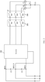
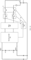
- FIG. 3 is a schematic diagram of a power converter according to this embodiment of this application.
- the power converter provided in this embodiment includes a power conversion circuit 101, a switching device, and a controller 102.
- Power conversion includes N phases, where N is 2 or 3. In this embodiment, N is 3. To be specific, a three-phase power converter and a three-phase alternating current power grid are used as examples.
- An input end of the power conversion circuit 101 is connected to a direct current power supply, and converts a direct current output by the direct current power supply into an alternating current.
- the switching device includes at least the following two stages: a first-stage switching device and a second-stage switching device.
- the first-stage switching device includes a first switch to an N th switch
- the second-stage switching device includes an (N+1) th switch to a 2N th switch.
- the first-stage switching device includes K1, K2, and K3, and the second-stage switching device includes K4, K5, and K6.
- K1 and K4 are connected in series in a phase C
- K2 and K5 are connected in series in a phase B
- K3 and K6 are connected in series in a phase A.
- first-stage switching device is close to an output end of the power conversion circuit 101, or the second-stage switching device may be close to the output end of the power conversion circuit 101.
- the output end of the power conversion circuit 101 is connected to the alternating current power grid through the first-stage switching device and the second-stage switching device that are connected in series.
- the controller 102 When the power conversion circuit 101 is connected to the alternating current power grid, the controller 102 first controls, by using a first control signal 24, the second-stage switching device (K4 to K6) to be turned on, and then sequentially controls the N switches in the first-stage switching device to be turned on one by one.
- a sequence of turning on the N switches in the first-stage switching device is not specifically limited in this embodiment of this application.
- a control signal 21 may be used to control K1 to be turned on first, then a control signal 22 may be used to control K2 to be turned on, and finally a control signal 23 may be used to control K3 to be turned on.
- K2 When the power conversion circuit 101 needs to be connected to the alternating current power grid next time, K2 may be controlled to turn on first, then K3 may be controlled to turn on, and finally K1 may be controlled to be turned on.
- No enumeration is provided herein.
- a purpose of such control is to control one switch in K1 to K3 to be first turned on in turn, so that the switch turned on for the first time bears a relatively large impulse current. In this way, the three switches are first turned on in turn to bear the impulse current in turn, instead of making one of the switches bear the impulse current each time. Therefore, an average life of the three switches can be prolonged.
- the power converter is an inverter and the power conversion circuit in the power converter is an inverter circuit.
- the first-stage switching device is first turned on, to be specific, K4 to K6 are simultaneously turned on because K4 to K6 are corresponding to a same control signal 24; and in the first-stage switching device, K1 is first turned on, and then K2 and K3 are sequentially turned on. In FIG. 4 , K2 and K3 are still in a turn-off state.
- a service life of a switching device is calculated based on a quantity of actions. A larger quantity of actions indicates a shorter service life. Therefore, controlling each switch in the first-stage switching device to be first turned on in turn can prolong the service life of the switches.
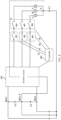
- FIG. 5 is a schematic diagram of an inverter including a filter according to an embodiment of this application.
- the inverter circuit 101, the filter 400, and the relays K1 to K6 are all integrated inside the inverter.
- the filter 400 mainly filters a voltage and a current that are output by the inverter circuit 101 and feeds back the voltage and the current to the alternating current power grid.
- the inverter provided in this embodiment of this application first controls K4 to K6 to be simultaneously turned on, and then uses three different signals to sequentially control K1 to K3 to be turned on.
- a sequence of K1 to K3 is not limited, but K1 to K3 need to be turned on at different moments.
- FIG. 6 is a schematic diagram of a short circuit fault according to an embodiment of this application.
- FIG. 6 a circuit diagram corresponding to only one phase is shown in FIG. 6 .
- an inverter circuit is a three-level inverter circuit is used for description.
- a location of the short circuit fault is a cable-to-ground short circuit fault at BUS-.
- a PE potential is positive relative to the power grid voltage.
- a loop is formed by using a connection to body diodes (D 1 and D2) of switching transistors in the three-level inverter circuit through BUS- and by passing through inductors (L1 and L2) and relays (K1 and K4). As the voltage is relatively high and a current increases rapidly, the relays need to be turned off at this time for protection, so as to prevent the fault from further spreading.
- relays in three phases in second-stage switching device is controlled to be simultaneously turned off, because there is a misphase between currents in the three phases and also a misphase between voltages in the three phases (in other words, it is impossible for the phases to be the same), simultaneously turning off the relays in three phases easily causes contact adhesion when a current in a phase is relatively small or crosses zero and currents in the other two phases are relatively large. As a result, the relays cannot be completely turned off, further spreading the fault. Therefore, when the relays in the three phases are controlled by linkage to be simultaneously turned off, turn-off capabilities of the relays are limited.
- the three phases may be sequentially disconnected, instead of being simultaneously disconnected. This can ensure that when a current of each phase is relatively small, a relay in the phase is turned off, thereby avoiding contact adhesion of the relay caused by an excessively large current.
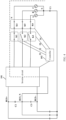
- FIG. 7 is a schematic diagram of another inverter according to an embodiment of this application.
- the controller 102 is further configured to: when the inverter circuit 101 is disconnected from the alternating current power grid, first sequentially control, based on output currents in the N phases of the inverter circuit, the N switches in the first-stage switching device to be turned off (to be specific, K1 to K3 are sequentially turned off, and a sequence of turning off K1 to K3 is not limited). Specifically, a relay of a phase is controlled to turn off only when a current corresponding to the phase is smaller than a preset current value, and all the three phases are controlled in this manner. Because the relays in the three phases are separately controlled, the relay in each phase is turned off when the current is relatively small, so that the relay can be successfully turned off without causing contact adhesion due to an excessively large current. Then, N switches in the second-stage switching device are all controlled to be turned off, to be specific, K4 to K6 are controlled to be simultaneously turned off first.
- N+1 control signals are also included.
- the controller 102 is configured to sequentially output a second turn-off signal to an (N+1) th turn-off signal, that is, turn-off signals 31 to 33, to control respectively the N switches (K1 to K3) in the first-stage switching device to be turned off.
- Turn-off timings of K1 to K3 may be determined based on the currents of the corresponding phases.
- a corresponding relay is controlled to turn off when the current is small.
- a first turn-off signal 34 is output to control all the N switches in the second-stage switching device to be turned off (that is, all of K4 to K6 are turned off).
- the controller 102 may include four interfaces (for example, I/O interfaces) connected to the relays.
- the four interfaces may output different signal states for turn-on and turn-off. For example, when the interface outputs a high-level signal, a relay is controlled to turn on correspondingly; and when the interface outputs a low-level signal, a relay is controlled to turn off correspondingly.
- a first interface is connected to the second-stage switching device to perform linked control on the second-stage switching device.
- a second interface to a fourth interface are connected to K1 to K3 in the first-stage switching device respectively, and the three relays K1 to K3 are controlled respectively by using the three interfaces, that is, the second interface to the fourth interface.
- a short circuit current has a same phase as the power grid voltage. Therefore, a zero-crossing point of the current basically coincides with a zero-crossing point of the voltage.
- the relay can be controlled to turn off by detecting the zero-crossing point of the voltage, or the relay can be controlled to turn off by detecting the zero-crossing point of the current.
- a specific detection location may be at an output end of the inverter circuit.
- a turn-off delay time of the relay may be obtained based on an actual application scenario. For example, if there is a time period t1 before the zero-crossing moment of the current, a turn-off delay time td and t1 need to be comprehensively considered to ensure precise control on a turn-off moment of the relay. To be specific, the delay td needs to be deducted from t1.
- the turn-off delay time of the relay may be tested based on the actual application scenario and set based on an empirical value obtained in the test.
- the controller 102 outputs, based on a preset turn-off delay time and the zero-crossing moment of the current in the i th phase, a turn-off drive signal to the switch in the i th phase in the first-stage switching device, where the turn-off drive signal is used to turn off the switch in the i th phase.
- the controller 102 controls the inverter circuit to be disconnected from the alternating current power grid, to prevent the short circuit fault from being spread to the power grid.
- a zero-crossing moment of a current in each phase is first determined. For example, a current in the phase C crosses zero first, that is, K1 is turned off. Then, zero-crossing moments in a phase A and a phase B continue to be determined, and based on the zero-crossing moments, K2 or K3 is controlled to be turned off. For example, if zero crossing occurs in the phase A next, K3 is turned off. K2 is turned off in the same way. Then, K4 to K6 are simultaneously turned off. At this point, all relays are turned off, and the inverter is completely disconnected from the alternating current power grid.
- a relay corresponding to the phase may be precisely controlled to be turned off. This avoids contact adhesion and turn-off failure of the relay caused by an excessively large current.
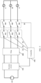
- FIG. 9 is a schematic diagram of a two-phase power converter according to an embodiment of this application.
- the power converter is an inverter and an output end of the inverter includes a filter is used for description.
- the output end of the inverter circuit 101 is connected to direct current bus capacitors C1 and C2.
- a direct-current-side input end of the inverter circuit 101 is a direct current bus, and BUS+ and BUS-correspond to a positive input end and a negative input end of the inverter circuit 101 respectively.
- the following first describes a working principle of controlling the switching device to turn on.
- FIG. 10 is a schematic diagram showing that a switching device is controlled to turn on according to an embodiment of this application.
- the first-stage switching device includes K1 and K2, and the second-stage switching device includes K3 and K4.
- a controller 102 first controls one stage of switching devices to be turned on, for example, first controls the second-stage switching device to be turned on, to be specific, uses a control signal 23 to control, by linkage, K3 and K4 to be simultaneously turned on. Then, the controller 102 uses control signals 21 and 22 to control respectively K1 and K2 to be sequentially turned on. To be specific, K1 is turned on first, and K2 is turned on later.
- a sequence of turning on K1 and K2 may be changed. For example, K1 is turned on first, and K2 is turned on later.
- K3 and K4 are already turned on and K1 is also turned on, when K2 is turned on, two tends of K2 do not need to bear an impact of a large voltage difference, thereby reducing damage to K2 and prolonging a life of K2.
- K1 and K2 may alternately be used as a switching device that is first turned on.
- the controller 102 needs to output three independent control signals.
- Three turn-on signals are correspondingly output, for example, 21, 22, and 23 in the figure, to turn on the switching device.
- the switching device needs to be turned off
- an example in which the switching device needs to be turned off when a short circuit to ground fault occurs is used for description. This is also applicable to other scenarios in which a switching device needs to be turned off.
- FIG. 11 is a schematic diagram showing that a switching device corresponding to two phases are turned off according to an embodiment of this application.
- the following uses an example in which the switching device needs to be turned off when a short circuit fault occurs and the switching device is a relay for description.
- the controller 102 outputs three independent turn-off signals 31, 32, and 33. At a zero-crossing moment of a current of a phase, the controller 102 first outputs the turn-off signal 32 to control K1 to be turned off, to ensure that K1 is effectively turned off and no contact adhesion occurs in K1 due to an excessively large current. Then, the controller 102 outputs the turn-off signal 22 to control K2 to be turned off. Finally, the controller 102 outputs the turn-off signal 33 to control K3 and K4 to be simultaneously turned off, that is, performs linkage control on K3 and K4.
- connection relationships between the controller 102 and the switching device include three interfaces, for example, I/O interfaces.
- the three interfaces of the controller 102 output high levels when the relays are controlled to be turned on, and the three interfaces output low levels when the relays are controlled to be turned off.
- the interfaces may be other output interfaces of the controller 102, for example, pulse drive signal pins.
- a turn-off delay time of the relay may be considered.
- the relay may be controlled to turn off based on a time obtained after the turn-off delay time of the relay is deducted from the zero-crossing moment of the current of the phase. This can ensure that the relay is turned off at an actual zero-crossing moment of the current, thereby reducing a turn-off loss and ensuring that the relay is successfully turned off without contact adhesion.
- currents in the three phases may be collected and the zero-crossing moments of the currents may be obtained by using current sampling signals, to determine zero-crossing moments of currents.
- a specific turn-off delay time needs to be tested according to an actual application scenario and relay type selection, and set based on an empirical value obtained during the test. Because the turn-off delay time of the relay is related to a current ambient temperature, a drive signal of the relay, and the like, no fixed turn-off delay time can be set. The turn-off delay time may be affected by both a temperature change and a drive signal change.
- N switches in the second-stage switching device are integrated in one housing.
- N when N is 3, three relays included in the second-stage switching device are all located in one housing and controlled by one control signal.
- N switches included in the first-stage switching device are separately disposed.
- three relays included in the first-stage switching device are separately disposed and each is controlled by using one independent control signal.
- N is 2.
- Two relays included in the second-stage switching device are both located in one housing and controlled by one control signal.
- Two relays included in the first-stage switching device are separately disposed and each is controlled by using one independent control signal.
- the N switches in the first-stage switching device may alternatively be integrated inside one housing, but N corresponding independent control signals are required to control the switches.
- the power converter provided in this embodiment of this application needs to use N+1 control signals to separately control 2N switching devices of N phases.
- the switching devices can be controlled sequentially to prolong their service lives, and a quantity of control signals can be minimized to improve control stability.
- FIG. 12 is a schematic diagram of an inverter including a DC-DC conversion circuit.
- An input end of a DC-DC conversion circuit 500 is connected to a direct current power supply.
- An output end of the DC-DC conversion circuit 500 is connected to an input end of an inverter circuit 102.
- FIG. 13 is a schematic diagram of a two-phase inverter including a DC-DC conversion circuit.
- this embodiment of this application further provides a photovoltaic power generation system, which includes the power converter described in the foregoing embodiments, and further includes a photovoltaic array.
- a photovoltaic power generation system which includes the power converter described in the foregoing embodiments, and further includes a photovoltaic array.
- FIG. 14 is a schematic diagram of a photovoltaic power generation system corresponding to a single-stage power converter according to an embodiment of this application.
- the following still uses a three-phase power converter and a three-phase power grid as an example for description.
- the description is provided by using an example in which a power conversion circuit included in the power converter is an inverter circuit.
- the inverter circuit may work bidirectionally, to be specific, may implement inversion in a forward direction and rectification in a reverse direction.
- an alternating current of the alternating current power grid may be rectified into a direct current to charge an energy storage device.
- An input end of an inverter circuit 101 is connected to a photovoltaic array 1000.
- the photovoltaic array 1000 provides a direct current power supply for the inverter circuit 101.
- the inverter circuit 101 may invert a direct current output by the photovoltaic array 1000 into an alternating current and feed back the alternating current to the three-phase alternating current power grid.
- turn-on of the switching device for example, a relay
- the switching device for example, a relay
- service lives of the relays can be prolonged.
- turn-off times of the relays can be precisely controlled, thereby ensuring that the relays are effectively turned off without contact adhesion and reducing switch damage on the relays.
- FIG. 15 is a schematic diagram of a photovoltaic power generation system corresponding to a two-stage power converter according to an embodiment of this application.
- the power converter includes a DC-DC conversion circuit 500 and an inverter circuit 101, and an input end of the DC-DC conversion circuit 500 is connected to a photovoltaic array 1000.
- a plurality of DC-DC conversion circuits may be connected in parallel to an input end of the inverter circuit, and an input end of each DC-DC conversion circuit is connected to a different photovoltaic array.
- the plurality of DC-DC conversion circuits when the plurality of DC-DC conversion circuits are connected in parallel, the plurality of DC-DC conversion circuits may be located inside a combiner box.
- the DC-DC conversion circuit may be a boost circuit Boost circuit, a buck circuit Buck circuit, or a buck-boost circuit BuckBoost circuit.
- the inverter circuit may be a two-level inverter circuit or a multi-level inverter circuit, for example, a three-level inverter circuit, provided that a quantity of levels of the DC-DC conversion circuit is the same as a quantity of levels of the inverter circuit.
- this embodiment of this application further provides a method for controlling an action of a switching device.
- the inverter circuit may be a bidirectional conversion circuit, to be specific, implement an inversion function in a forward direction and a rectification function in a reverse direction.
- FIG. 16 is a flowchart of a method for turning on a switching device according to an embodiment of this application.
- the method for controlling an action of a switching device provided in this embodiment is applied to the power converter provided in the foregoing embodiments.
- the power converter includes an inverter circuit and a switching device.
- the power converter includes N phases, where N is 2 or 3. In other words, the power converter may be two-phase or three-phase.
- An output end of the inverter circuit is connected to an alternating current power grid through a first-stage switching device and a second-stage switching device that are connected in series.
- the switching device includes the following two stages: a first-stage switching device and a second-stage switching device.
- the first-stage switching device and the second-stage switching device separately include N switches, to be specific, include 2N switches in total, for example, include four switches in case of two phases, and six switches in case of three phases.
- the method includes the following steps.
- the sequentially controlling the N switches in the first-stage switching device to be separately turned on specifically includes: when the inverter circuit is connected to the alternating current power grid this time, changing a sequence of separately turning on the N switches in the first-stage switching device.
- the foregoing describes how to control the switching device to turn on when the inverter circuit is controlled to be connected to the power grid.
- the following describes how to control the switching device to turn off when the inverter circuit is disconnected from the power grid. For example, it is determined whether a short circuit fault occurs at an input end or the output end of the inverter circuit. For example, whether a short circuit to ground fault occurs at an input end BUS- of the inverter circuit may be determined based on a detection voltage.
- the detection voltage may be compared with a preset voltage threshold. When the detection voltage is less than the preset voltage threshold, it indicates that a short circuit fault occurs.
- whether a short circuit fault occurs may alternatively be determined based on a detection current. For example, the detection current is compared with a preset current threshold. When the detection current is greater than the preset current threshold, it indicates that a short circuit fault occurs.
- the inverter circuit needs to be controlled to be disconnected from the alternating current power grid.
- FIG. 17 is a flowchart of a method for turning off a switching device according to an embodiment of this application.
- S1603 First sequentially control, based on output currents in the N phases of the inverter circuit, the N switches in the first-stage switching device to be separately turned off.
- a switching device in the phase A is controlled to turn off first, following by a switching device in a phase B and finally a switching device in a phase C.
- a turn-off delay of the switching device is considered. In other words, a preset turn-off delay time is specified.
- the controlling a switch in the i th phase in the first-stage switching device to be turned off specifically includes: based on a preset turn-off delay time and the zero-crossing moment of the current in the i th phase, outputting a turn-off drive signal to the switch in the i th phase in the first-stage switching device, where the turn-off drive signal is used to turn off the switch in the i th phase.
- currents in the three phases may be collected and the zero-crossing moments of the currents may be obtained by using current sampling signals, to determine zero-crossing moments of currents.
- the zero-crossing moments of the currents may be determined by using a hardware circuit or software. This is not specifically limited herein.
- the switches in the N phases are not controlled as a whole at a time.
- a quantity of control signals is minimized, to effectively balance decentralized and independent control on the switching devices and reliability, because a larger quantity of control signals leads to higher vulnerability to interference and lower stability.
- the switching devices are controlled as decentralizedly as possible while stability and controllability are ensured, thereby resolving the technical problem of a current shock occurring simultaneously in the switching devices in the three phases.
- this embodiment of this application further provides an apparatus for controlling an action of a switching device.
- FIG. 18 is a schematic diagram of an apparatus for controlling an action of a switching device according to an embodiment of this application.
- the apparatus for controlling an action of a switching device is applied to a power converter.
- the power converter includes a power conversion circuit and a switching device.
- the switching device includes a first-stage switching device and a second-stage switching device.
- the power converter includes N phases, where N is 2 or 3.
- An output end of the power conversion circuit is connected to an alternating current power grid through the first-stage switching device and the second-stage switching device that are connected in series.
- the first-stage switching device and the second-stage switching device separately include N switches.
- the apparatus includes a first turn-on control unit 1801 and a second turn-on control unit 1802.
- the first turn-on control unit 1801 is configured to: when the power conversion circuit is connected to the alternating current power grid, first control the N switches in the second-stage switching device to be simultaneously turned on.
- the second turn-on control unit 1802 is configured to: after the N switches in the second-stage switching device are simultaneously turned on, sequentially control the N switches in the first-stage switching device to be turned on one by one.
- the second turn-on control unit includes a replacement subunit.
- the replacement subunit is configured to: when the power conversion circuit is connected to the alternating current power grid this time, change a sequence of separately turning on the N switches in the first-stage switching device.
- the apparatus provided in this embodiment further includes a first turn-off control unit and a second turn-off control unit.
- the first turn-off control unit is configured to: when the power conversion circuit is disconnected from the alternating current power grid, first sequentially control, based on output currents in the N phases of the power conversion circuit, the N switches in the first-stage switching device to be separately turned off.
- the second turn-off control unit is configured to: after the N switches in the first-stage switching device are all turned off, control the N switches in the second-stage switching device to be simultaneously turned off.
- the first turn-off control unit specifically includes a current detection subunit and a turn-off control subunit.
- the current detection subunit is configured to detect a zero-crossing moment of a current in an i th phase in the output currents in the N phases of the power conversion circuit.
- the turn-off control subunit is specifically configured to: based on a preset turn-off delay time and the zero-crossing moment of the current in the i th phase, output a turn-off signal to the switch in the i th phase in the first-stage switching device, where the turn-off signal is used to turn off the switch in the i th phase.
- the apparatus provided in this embodiment further includes a determining unit, configured to determine whether a short circuit fault occurs at an input end or the output end of the power conversion circuit. If a short circuit fault occurs at the input end or the output end of the power conversion circuit, the first turn-off control unit and the second turn-off control unit control the power conversion circuit to be disconnected from the alternating current power grid.
- first and second are used for differentiation, and do not indicate an order or a meaning.
- At least one piece (item) means one or more, and "a plurality of means two or more.
- the term “and/or” is used to describe an association relationship between associated objects, and represents that three relationships may exist.
- a and/or B may represent the following three cases: Only A exists, only B exists, and both A and B exist, where A and B may be singular or plural.
- the character “/” generally indicates an “or” relationship between the associated objects.
- At least one of the following items (pieces) or a similar expression thereof indicates any combination of these items, including a single item (piece) or any combination of a plurality of items (pieces).
- At least one item (piece) of a, b, or c may represent: a, b, c, "a and b", “a and c", “b and c", or "a, b, and c", where a, b, and c may be singular or plural.
Landscapes
- Engineering & Computer Science (AREA)
- Power Engineering (AREA)
- Inverter Devices (AREA)
- Photovoltaic Devices (AREA)
- Charge And Discharge Circuits For Batteries Or The Like (AREA)
- Control Of Electrical Variables (AREA)
- Dc-Dc Converters (AREA)
Applications Claiming Priority (2)
| Application Number | Priority Date | Filing Date | Title |
|---|---|---|---|
| CN202010910289.6A CN112234645B (zh) | 2020-09-02 | 2020-09-02 | 一种功率变换器、光伏发电系统、方法及装置 |
| PCT/CN2021/108583 WO2022048345A1 (zh) | 2020-09-02 | 2021-07-27 | 一种功率变换器、光伏发电系统、方法及装置 |
Publications (2)
| Publication Number | Publication Date |
|---|---|
| EP4199293A1 true EP4199293A1 (de) | 2023-06-21 |
| EP4199293A4 EP4199293A4 (de) | 2024-04-24 |
Family
ID=74116669
Family Applications (1)
| Application Number | Title | Priority Date | Filing Date |
|---|---|---|---|
| EP21863413.7A Pending EP4199293A4 (de) | 2020-09-02 | 2021-07-27 | Stromwandler, fotovoltaisches stromerzeugungssystem sowie verfahren und vorrichtung |
Country Status (5)
| Country | Link |
|---|---|
| US (1) | US12184201B2 (de) |
| EP (1) | EP4199293A4 (de) |
| CN (1) | CN112234645B (de) |
| AU (1) | AU2021336496B2 (de) |
| WO (1) | WO2022048345A1 (de) |
Cited By (2)
| Publication number | Priority date | Publication date | Assignee | Title |
|---|---|---|---|---|
| EP4586439A3 (de) * | 2024-01-15 | 2025-08-13 | Huawei Digital Power Technologies Co., Ltd. | Ein-/aus-gitter-schaltvorrichtung und stromversorgungssystem |
| EP4601176A1 (de) * | 2024-02-08 | 2025-08-13 | Sungrow Power Supply Co., Ltd. | Wechselrichter, verfahren zum abschalten eines wechselrichters und fotovoltaisches system |
Families Citing this family (6)
| Publication number | Priority date | Publication date | Assignee | Title |
|---|---|---|---|---|
| CN112234645B (zh) | 2020-09-02 | 2022-10-04 | 华为数字能源技术有限公司 | 一种功率变换器、光伏发电系统、方法及装置 |
| CN115065263B (zh) * | 2022-06-24 | 2025-09-02 | 阳光电源股份有限公司 | 一种三电平逆变器、光伏系统及控制方法 |
| CN117239684A (zh) * | 2023-09-14 | 2023-12-15 | 阳光电源股份有限公司 | 一种逆变器及其异常关断方法和装置、一种光伏系统 |
| US20250210971A1 (en) * | 2023-12-21 | 2025-06-26 | Shanghai Sigeyuan Intelligent Technology Co.,Ltd | Protection Circuit, Control Method and Photovoltaic System |
| CN118040616A (zh) * | 2024-02-08 | 2024-05-14 | 阳光电源股份有限公司 | 一种逆变器、一种逆变器关断方法及一种光伏系统 |
| CN121710129A (zh) * | 2024-09-18 | 2026-03-20 | 阳光电源股份有限公司 | 逆变器、逆变器的短路保护方法和能源系统 |
Family Cites Families (14)
| Publication number | Priority date | Publication date | Assignee | Title |
|---|---|---|---|---|
| EP2148417B1 (de) * | 2008-07-22 | 2018-01-10 | SMA Solar Technology AG | Wechselrichterschaltungsanordnung für einen Photovoltaikgenerator mit mehreren eingangs seriell geschalteten Stromrichtern |
| DK2228895T3 (da) | 2009-03-09 | 2013-04-08 | Sma Solar Technology Ag | Vekselretter med netværksgrænseflade |
| CN103312139B (zh) | 2012-03-09 | 2016-05-11 | 台达电子工业股份有限公司 | 一种并网逆变器的启动装置及其控制方法 |
| CN202712870U (zh) | 2012-05-03 | 2013-01-30 | 阳光电源股份有限公司 | 继电器装置及具有该继电器装置的逆变器及发电系统 |
| CN103683472A (zh) * | 2013-12-04 | 2014-03-26 | 深圳科士达新能源有限公司 | 具有不间断电源功能的混合逆变器 |
| CN104009658B (zh) * | 2014-05-28 | 2017-01-11 | 华为技术有限公司 | 功率变换电路和功率变换系统 |
| CN104868739B (zh) * | 2015-05-13 | 2017-03-15 | 西安西驰电能技术有限公司 | 一种基于三电平直流母线的dc‑dc开关电源系统 |
| JP6889013B2 (ja) * | 2017-04-19 | 2021-06-18 | 田淵電機株式会社 | 電力変換装置及び分散型電源システム |
| CN107086806B (zh) * | 2017-05-17 | 2024-01-09 | 中国铁道科学研究院集团有限公司 | 一种辅助变流器及其控制方法 |
| CN207442732U (zh) * | 2017-09-21 | 2018-06-01 | 无锡联动太阳能科技有限公司 | 一种太阳能发电系统 |
| RU2700594C1 (ru) * | 2018-11-07 | 2019-09-18 | Общество с ограниченной ответственностью "Транспортные прогрессивные технологии" | Силовой выпрямительно-инверторный преобразователь однофазного переменного тока для электрического транспорта и способ его управления |
| CN109510490A (zh) * | 2018-12-29 | 2019-03-22 | 河南锂想动力科技有限公司 | 一种多功能交直流电源系统 |
| CN112868175A (zh) * | 2019-01-28 | 2021-05-28 | 华为技术有限公司 | 一种解决共模电压干扰的设备、方法及系统 |
| CN112234645B (zh) * | 2020-09-02 | 2022-10-04 | 华为数字能源技术有限公司 | 一种功率变换器、光伏发电系统、方法及装置 |
-
2020
- 2020-09-02 CN CN202010910289.6A patent/CN112234645B/zh active Active
-
2021
- 2021-07-27 WO PCT/CN2021/108583 patent/WO2022048345A1/zh not_active Ceased
- 2021-07-27 AU AU2021336496A patent/AU2021336496B2/en active Active
- 2021-07-27 EP EP21863413.7A patent/EP4199293A4/de active Pending
-
2023
- 2023-02-28 US US18/175,583 patent/US12184201B2/en active Active
Cited By (3)
| Publication number | Priority date | Publication date | Assignee | Title |
|---|---|---|---|---|
| EP4586439A3 (de) * | 2024-01-15 | 2025-08-13 | Huawei Digital Power Technologies Co., Ltd. | Ein-/aus-gitter-schaltvorrichtung und stromversorgungssystem |
| EP4601176A1 (de) * | 2024-02-08 | 2025-08-13 | Sungrow Power Supply Co., Ltd. | Wechselrichter, verfahren zum abschalten eines wechselrichters und fotovoltaisches system |
| AU2024287078B2 (en) * | 2024-02-08 | 2026-03-19 | Sungrow Power Supply Co., Ltd. | Inverter, method for turning off inverter, and photovoltaic system |
Also Published As
| Publication number | Publication date |
|---|---|
| WO2022048345A1 (zh) | 2022-03-10 |
| AU2021336496B2 (en) | 2024-05-02 |
| CN112234645B (zh) | 2022-10-04 |
| US12184201B2 (en) | 2024-12-31 |
| US20230208312A1 (en) | 2023-06-29 |
| AU2021336496A1 (en) | 2023-04-13 |
| EP4199293A4 (de) | 2024-04-24 |
| CN112234645A (zh) | 2021-01-15 |
Similar Documents
| Publication | Publication Date | Title |
|---|---|---|
| US12184201B2 (en) | Power converter, photovoltaic power generation system, method, and apparatus | |
| US20230396057A1 (en) | Photovoltaic system, direct-current combiner box, and fault isolation method | |
| EP3567711B1 (de) | Modul zur unterdrückung des einschaltstroms, verfahren zur steuerung davon und bidirektionales ladegerät damit | |
| EP4195483A1 (de) | Gleichstrom-kombinatorbox, wechselrichter, fotovoltaisches system und schutzverfahren | |
| JP6417043B2 (ja) | 電力変換装置 | |
| US12355253B2 (en) | Photovoltaic system, protection method, and inverter system | |
| EP3531531A1 (de) | Verfahren zum laden eines submodulbasierten hybridwandlers | |
| US20150003127A1 (en) | Multilevel power conversion circuit | |
| US10122261B2 (en) | Power conversion device | |
| EP4016828B1 (de) | Gleichspannungswandlerschaltung | |
| CN114629370B (zh) | 功率变换系统、功率变换系统的控制方法及电力系统 | |
| US9859809B2 (en) | Power conversion device | |
| CN115514220A (zh) | 一种升降压变换器及电源系统 | |
| US20260012003A1 (en) | Photovoltaic system and control method | |
| CN113922685B (zh) | 一种基于单相t型三电平h桥的级联型固态变压器故障容错调制方法 | |
| CN113572370A (zh) | 一种智能整流回馈共直流母线系统及控制方法 | |
| CN210350806U (zh) | 储能逆变器中双向ac/dc变换器交流侧的路由继电器电路 | |
| CN103326385A (zh) | 具有低电压穿越电源装置的给粉机变频器控制系统 | |
| US10075091B2 (en) | Power converter | |
| CN113949273B (zh) | 一种低纹波深空探测器电源系统 | |
| CN101162843B (zh) | 复合式不间断供电电源 | |
| CN112491270A (zh) | 一种升压电路及其装置和系统 | |
| CN212969069U (zh) | 一种光伏逆变器 | |
| CN213461230U (zh) | 一种智能柔性电源切换装置 | |
| CN223713590U (zh) | 大功率直流变换电路及电动车辆 |
Legal Events
| Date | Code | Title | Description |
|---|---|---|---|
| STAA | Information on the status of an ep patent application or granted ep patent |
Free format text: STATUS: THE INTERNATIONAL PUBLICATION HAS BEEN MADE |
|
| PUAI | Public reference made under article 153(3) epc to a published international application that has entered the european phase |
Free format text: ORIGINAL CODE: 0009012 |
|
| STAA | Information on the status of an ep patent application or granted ep patent |
Free format text: STATUS: REQUEST FOR EXAMINATION WAS MADE |
|
| 17P | Request for examination filed |
Effective date: 20230315 |
|
| AK | Designated contracting states |
Kind code of ref document: A1 Designated state(s): AL AT BE BG CH CY CZ DE DK EE ES FI FR GB GR HR HU IE IS IT LI LT LU LV MC MK MT NL NO PL PT RO RS SE SI SK SM TR |
|
| DAV | Request for validation of the european patent (deleted) | ||
| DAX | Request for extension of the european patent (deleted) | ||
| A4 | Supplementary search report drawn up and despatched |
Effective date: 20240325 |
|
| RIC1 | Information provided on ipc code assigned before grant |
Ipc: H02M 7/72 20060101ALI20240319BHEP Ipc: H02S 40/32 20140101ALI20240319BHEP Ipc: H02M 7/48 20070101ALI20240319BHEP Ipc: H02J 3/32 20060101ALI20240319BHEP Ipc: H02J 3/38 20060101AFI20240319BHEP |
|
| STAA | Information on the status of an ep patent application or granted ep patent |
Free format text: STATUS: EXAMINATION IS IN PROGRESS |
|
| 17Q | First examination report despatched |
Effective date: 20250409 |
|
| GRAP | Despatch of communication of intention to grant a patent |
Free format text: ORIGINAL CODE: EPIDOSNIGR1 |
|
| STAA | Information on the status of an ep patent application or granted ep patent |
Free format text: STATUS: GRANT OF PATENT IS INTENDED |
|
| INTG | Intention to grant announced |
Effective date: 20260313 |