EP4016828B1 - Gleichspannungswandlerschaltung - Google Patents
Gleichspannungswandlerschaltung Download PDFInfo
- Publication number
- EP4016828B1 EP4016828B1 EP20851876.1A EP20851876A EP4016828B1 EP 4016828 B1 EP4016828 B1 EP 4016828B1 EP 20851876 A EP20851876 A EP 20851876A EP 4016828 B1 EP4016828 B1 EP 4016828B1
- Authority
- EP
- European Patent Office
- Prior art keywords
- capacitor
- switch
- diode
- direct current
- terminal
- Prior art date
- Legal status (The legal status is an assumption and is not a legal conclusion. Google has not performed a legal analysis and makes no representation as to the accuracy of the status listed.)
- Active
Links
Images


Classifications
-
- H—ELECTRICITY
- H02—GENERATION; CONVERSION OR DISTRIBUTION OF ELECTRIC POWER
- H02M—APPARATUS FOR CONVERSION BETWEEN AC AND AC, BETWEEN AC AND DC, OR BETWEEN DC AND DC, AND FOR USE WITH MAINS OR SIMILAR POWER SUPPLY SYSTEMS; CONVERSION OF DC OR AC INPUT POWER INTO SURGE OUTPUT POWER; CONTROL OR REGULATION THEREOF
- H02M3/00—Conversion of DC power input into DC power output
- H02M3/22—Conversion of DC power input into DC power output with intermediate conversion into AC
- H02M3/24—Conversion of DC power input into DC power output with intermediate conversion into AC by static converters
- H02M3/28—Conversion of DC power input into DC power output with intermediate conversion into AC by static converters using discharge tubes with control electrode or semiconductor devices with control electrode to produce the intermediate AC
- H02M3/325—Conversion of DC power input into DC power output with intermediate conversion into AC by static converters using discharge tubes with control electrode or semiconductor devices with control electrode to produce the intermediate AC using devices of a triode or a transistor type requiring continuous application of a control signal
- H02M3/335—Conversion of DC power input into DC power output with intermediate conversion into AC by static converters using discharge tubes with control electrode or semiconductor devices with control electrode to produce the intermediate AC using devices of a triode or a transistor type requiring continuous application of a control signal using semiconductor devices only
- H02M3/3353—Conversion of DC power input into DC power output with intermediate conversion into AC by static converters using discharge tubes with control electrode or semiconductor devices with control electrode to produce the intermediate AC using devices of a triode or a transistor type requiring continuous application of a control signal using semiconductor devices only having at least two simultaneously operating switches on the input side, e.g. "double forward" or "double (switched) flyback" converter
-
- H—ELECTRICITY
- H02—GENERATION; CONVERSION OR DISTRIBUTION OF ELECTRIC POWER
- H02M—APPARATUS FOR CONVERSION BETWEEN AC AND AC, BETWEEN AC AND DC, OR BETWEEN DC AND DC, AND FOR USE WITH MAINS OR SIMILAR POWER SUPPLY SYSTEMS; CONVERSION OF DC OR AC INPUT POWER INTO SURGE OUTPUT POWER; CONTROL OR REGULATION THEREOF
- H02M1/00—Details of apparatus for conversion
- H02M1/0095—Hybrid converter topologies, e.g. NPC mixed with flying capacitor, thyristor converter mixed with MMC or charge pump mixed with buck
-
- H—ELECTRICITY
- H02—GENERATION; CONVERSION OR DISTRIBUTION OF ELECTRIC POWER
- H02M—APPARATUS FOR CONVERSION BETWEEN AC AND AC, BETWEEN AC AND DC, OR BETWEEN DC AND DC, AND FOR USE WITH MAINS OR SIMILAR POWER SUPPLY SYSTEMS; CONVERSION OF DC OR AC INPUT POWER INTO SURGE OUTPUT POWER; CONTROL OR REGULATION THEREOF
- H02M1/00—Details of apparatus for conversion
- H02M1/32—Means for protecting converters other than automatic disconnection
- H02M1/34—Snubber circuits
-
- H—ELECTRICITY
- H02—GENERATION; CONVERSION OR DISTRIBUTION OF ELECTRIC POWER
- H02M—APPARATUS FOR CONVERSION BETWEEN AC AND AC, BETWEEN AC AND DC, OR BETWEEN DC AND DC, AND FOR USE WITH MAINS OR SIMILAR POWER SUPPLY SYSTEMS; CONVERSION OF DC OR AC INPUT POWER INTO SURGE OUTPUT POWER; CONTROL OR REGULATION THEREOF
- H02M3/00—Conversion of DC power input into DC power output
- H02M3/02—Conversion of DC power input into DC power output without intermediate conversion into AC
- H02M3/04—Conversion of DC power input into DC power output without intermediate conversion into AC by static converters
- H02M3/10—Conversion of DC power input into DC power output without intermediate conversion into AC by static converters using discharge tubes with control electrode or semiconductor devices with control electrode
- H02M3/145—Conversion of DC power input into DC power output without intermediate conversion into AC by static converters using discharge tubes with control electrode or semiconductor devices with control electrode using devices of a triode or transistor type requiring continuous application of a control signal
- H02M3/155—Conversion of DC power input into DC power output without intermediate conversion into AC by static converters using discharge tubes with control electrode or semiconductor devices with control electrode using devices of a triode or transistor type requiring continuous application of a control signal using semiconductor devices only
-
- H—ELECTRICITY
- H02—GENERATION; CONVERSION OR DISTRIBUTION OF ELECTRIC POWER
- H02M—APPARATUS FOR CONVERSION BETWEEN AC AND AC, BETWEEN AC AND DC, OR BETWEEN DC AND DC, AND FOR USE WITH MAINS OR SIMILAR POWER SUPPLY SYSTEMS; CONVERSION OF DC OR AC INPUT POWER INTO SURGE OUTPUT POWER; CONTROL OR REGULATION THEREOF
- H02M1/00—Details of apparatus for conversion
- H02M1/0048—Circuits or arrangements for reducing losses
- H02M1/0054—Transistor switching losses
- H02M1/0058—Transistor switching losses by employing soft switching techniques, i.e. commutation of transistors when applied voltage is zero or when current flow is zero
-
- H—ELECTRICITY
- H02—GENERATION; CONVERSION OR DISTRIBUTION OF ELECTRIC POWER
- H02M—APPARATUS FOR CONVERSION BETWEEN AC AND AC, BETWEEN AC AND DC, OR BETWEEN DC AND DC, AND FOR USE WITH MAINS OR SIMILAR POWER SUPPLY SYSTEMS; CONVERSION OF DC OR AC INPUT POWER INTO SURGE OUTPUT POWER; CONTROL OR REGULATION THEREOF
- H02M1/00—Details of apparatus for conversion
- H02M1/32—Means for protecting converters other than automatic disconnection
- H02M1/34—Snubber circuits
- H02M1/344—Active dissipative snubbers
-
- H—ELECTRICITY
- H02—GENERATION; CONVERSION OR DISTRIBUTION OF ELECTRIC POWER
- H02M—APPARATUS FOR CONVERSION BETWEEN AC AND AC, BETWEEN AC AND DC, OR BETWEEN DC AND DC, AND FOR USE WITH MAINS OR SIMILAR POWER SUPPLY SYSTEMS; CONVERSION OF DC OR AC INPUT POWER INTO SURGE OUTPUT POWER; CONTROL OR REGULATION THEREOF
- H02M3/00—Conversion of DC power input into DC power output
- H02M3/02—Conversion of DC power input into DC power output without intermediate conversion into AC
- H02M3/04—Conversion of DC power input into DC power output without intermediate conversion into AC by static converters
- H02M3/06—Conversion of DC power input into DC power output without intermediate conversion into AC by static converters using resistors or capacitors, e.g. potential divider
- H02M3/07—Conversion of DC power input into DC power output without intermediate conversion into AC by static converters using resistors or capacitors, e.g. potential divider using capacitors charged and discharged alternately by semiconductor devices with control electrode, e.g. charge pumps
-
- H—ELECTRICITY
- H02—GENERATION; CONVERSION OR DISTRIBUTION OF ELECTRIC POWER
- H02M—APPARATUS FOR CONVERSION BETWEEN AC AND AC, BETWEEN AC AND DC, OR BETWEEN DC AND DC, AND FOR USE WITH MAINS OR SIMILAR POWER SUPPLY SYSTEMS; CONVERSION OF DC OR AC INPUT POWER INTO SURGE OUTPUT POWER; CONTROL OR REGULATION THEREOF
- H02M3/00—Conversion of DC power input into DC power output
- H02M3/02—Conversion of DC power input into DC power output without intermediate conversion into AC
- H02M3/04—Conversion of DC power input into DC power output without intermediate conversion into AC by static converters
- H02M3/10—Conversion of DC power input into DC power output without intermediate conversion into AC by static converters using discharge tubes with control electrode or semiconductor devices with control electrode
- H02M3/145—Conversion of DC power input into DC power output without intermediate conversion into AC by static converters using discharge tubes with control electrode or semiconductor devices with control electrode using devices of a triode or transistor type requiring continuous application of a control signal
- H02M3/155—Conversion of DC power input into DC power output without intermediate conversion into AC by static converters using discharge tubes with control electrode or semiconductor devices with control electrode using devices of a triode or transistor type requiring continuous application of a control signal using semiconductor devices only
- H02M3/156—Conversion of DC power input into DC power output without intermediate conversion into AC by static converters using discharge tubes with control electrode or semiconductor devices with control electrode using devices of a triode or transistor type requiring continuous application of a control signal using semiconductor devices only with automatic control of output voltage or current, e.g. switching regulators
- H02M3/158—Conversion of DC power input into DC power output without intermediate conversion into AC by static converters using discharge tubes with control electrode or semiconductor devices with control electrode using devices of a triode or transistor type requiring continuous application of a control signal using semiconductor devices only with automatic control of output voltage or current, e.g. switching regulators including plural semiconductor devices as final control devices for a single load
Definitions
- This application relates to the field of photovoltaic power generation technologies, and in particular, to a direct current-direct current conversion circuit.
- An existing photovoltaic power generation system includes a photovoltaic module and a direct current converter, where the photovoltaic module is configured to convert solar energy into direct current electrical energy, and the direct current converter is configured to perform direct current conversion on the direct current electrical energy.
- a multi-level power conversion circuit has the following advantages: (1) Medium-high voltage and large-capacity power change can be implemented by using a power device with relatively low voltage capacity; (2) due to an increase in a quantity of levels, an output voltage waveform is of relatively high quality; (3) a change rate of a pulse voltage generated by one switching action is relatively low, so that an electromagnetic interference problem can be greatly alleviated; and (4) same harmonic quality requires a relatively low switching frequency, so that a switching loss can be reduced and power change efficiency can be improved.
- a direct current-direct current converter is usually designed as a multi-level power conversion circuit, so that not only the foregoing advantages can be utilized, but also a power device in the photovoltaic power generation system can be prevented from bearing an entire bus voltage.
- Embodiments of this application provide a direct current-direct current conversion circuit, which can work at three levels when no common mode current is generated.
- the invention is defined in the appended claims.
- Embodiments of this application provide a direct current-direct current conversion circuit, which can work at three levels when no common mode current is generated.
- FIG. 1 is a schematic architectural diagram of a photovoltaic power generation system according to an embodiment of this application.
- the photovoltaic power generation system includes a photovoltaic module, a direct current-direct current conversion circuit, storage batteries, an inverter circuit, a direct current load, an alternating current load, and a power grid.
- solar energy is converted into direct current electrical energy by the photovoltaic module, the direct current electrical energy is boosted by a direct current-direct current converter, the boosted direct current electrical energy may be directly supplied to the direct current load and stored into the storage batteries, or may continue to be converted into alternating current electrical energy by an inverter.
- the alternating current electrical energy may be supplied directly to the alternating current load or connected to the power grid.
- the direct current-direct current conversion circuit in the embodiments of this application is applied to the photovoltaic power generation system, so that no common mode current is generated, and the direct current-direct current conversion circuit can work at three levels.
- the direct current-direct current conversion circuit can work at three levels. To better understand a process of working by using three levels, a simple example is first used to describe the process of working by using three levels.
- FIG. 2 is a schematic diagram of a structure of a three-level conversion circuit.
- E1 and E2 are two direct current power supplies, a negative electrode of the direct current power supply E1 is connected to a positive electrode of the direct current power supply E2, and the connection point is grounded, that is, a reference voltage of the connection point is 0.
- a switch Sa and a switch Sc are connected in series between a positive electrode of the direct current power supply E1 and a negative electrode of the direct current power supply E2, one terminal of a switch Sb is connected between the negative electrode of the direct current power supply E1 and the positive electrode of the direct current power supply E2, and the other terminal is connected between the switch Sa and the switch Sc.
- states of the switches Sa, Sb, and Sc are different, output voltages Vout are different.
- the output voltage Vout is E1. If Sb is closed, and Sa and Sc are disconnected, the output voltage Vout is 0. If Sc is closed, and Sa and Sb are disconnected, the output voltage Vout is -E2. It can be learned that the circuit shown in FIG. 2 may output three levels: E1, 0, and -E2.
- the direct current-direct current conversion circuit in the embodiments of this application is formed by newly adding a component to a flying capacitor (flying capacitor) based boost chopper circuit.
- the direct current-direct current conversion circuit is also referred to as an active direct current-direct current conversion circuit.
- the direct current-direct current conversion circuit is also referred to as a passive direct current-direct current conversion circuit. Therefore, the active direct current-direct current conversion circuit and the passive direct current-direct current conversion circuit are separately described below.
- the active direct current-direct current conversion circuit is first described.
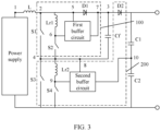
- FIG. 3 is a schematic diagram of a first embodiment of a direct current-direct current conversion circuit according to an embodiment of this application.
- An embodiment of this application provides the first embodiment of the direct current-direct current conversion circuit, including: an input inductor L, a first capacitor C1, a second capacitor C2, a flying capacitor Cf, a first soft switch unit 100, and a second soft switch unit 200.
- the first soft switch unit 100 includes a first switch S1, a second switch S2, a first inductor Lr1, a first diode D1, and a first buffer circuit; and the second soft switch unit 200 includes a third switch S3, a fourth switch S4, a second inductor Lr2, a second diode D2, and a second buffer circuit.
- the first switch S1, the second switch S2, the third switch S3, and the fourth switch S4 may be a metal-oxide semiconductor field effect transistor or an insulated gate bipolar transistor.
- a power supply, the input inductor L, the first diode D1, the second diode D2, the first capacitor C1, and the second capacitor C2 are sequentially connected in series, where a first terminal 1 of the input inductor L is connected to a positive electrode of the power supply, a second terminal 2 of the input inductor L is connected to a positive electrode of the first diode D1, and a negative electrode of the first diode D1 is connected to a positive electrode of the second diode D2.
- the power supply may be any circuit module that can output a current.
- the power supply may be a photovoltaic module.
- a first branch and a second branch are connected in parallel between the second terminal 2 of the input inductor L and a negative electrode of the power supply, the first branch includes the first switch S1 and the third switch S3 that are sequentially connected in series, the second branch includes the first inductor Lr1, the second switch S2, the second inductor Lr2, and the fourth switch S4 that are sequentially connected in series, and the first switch S1 and the first inductor Lr1 are both connected to the second terminal 2 of the input inductor L.
- the first inductor Lr1 is connected in series to the second switch S2, and the first inductor Lr1 and the second switch S2 are connected, as a whole, in parallel to two terminals of the first switch S1.
- the second inductor Lr2 is connected in series to the fourth switch S4, and the second inductor Lr2 and the fourth switch S4 are connected, as a whole, in parallel to two terminals of the third switch S3.
- a first terminal 3 of the flying capacitor Cf is connected between the first diode D1 and the second diode D2, a second terminal 4 of the flying capacitor Cf is connected between the first switch S1 and the third switch S3, and the second terminal 4 of the flying capacitor Cf is further connected between the second switch S2 and the second inductor Lr2.
- a first terminal 5 of the first buffer circuit is connected to the positive electrode of the first diode D1
- a second terminal 6 of the first buffer circuit is connected between the first inductor Lr1 and the second switch S2
- a third terminal 7 of the first buffer circuit is connected to the negative electrode of the first diode D1.
- the first buffer circuit is configured to transfer energy of the first inductor Lr1 to the flying capacitor Cf, or to the first capacitor C1 and the second capacitor C2.
- a first terminal 8 of the second buffer circuit is connected to the second terminal 4 of the flying capacitor Cf, a second terminal 9 of the second buffer circuit is connected between the second inductor Lr2 and the fourth switch S4, and a third terminal 10 of the second buffer circuit is connected between the first capacitor C1 and the second capacitor C2.
- the second buffer circuit is configured to transfer energy of the second inductor Lr2 to the second capacitor C2.
- the following analyzes working states of the direct current-direct current conversion circuit in this embodiment of this application based on the foregoing circuit structure.
- the input inductor L, the first capacitor C1, the second capacitor C2, and the flying capacitor Cf are all sufficiently large, to ensure that in a working process of the direct current-direct current conversion circuit, a voltage Vf of two terminals of the flying capacitor Cf and output voltages Vout of two terminals of the first capacitor C1 and of two terminals of the second capacitor C2 remain basically unchanged.
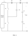
- the input inductor L, the first switch S1, the third switch S3, the first diode D1, the second diode D2, the flying capacitor Cf, the first capacitor C1, and the second capacitor C2 constitute the flying capacitor Cf based boost chopper circuit shown in FIG. 4 . It can be learned based on a working principle of the flying capacitor Cf based boost chopper circuit that, when the circuit shown in FIG. 4 works normally, an output voltage Vout is greater than a power supply voltage Vin, and voltages of the first capacitor C1 and the second capacitor C2 always remain the same. In addition, switching states of the first switch S1 and the third switch S3 are changed by using a control signal, so that the direct current-direct current conversion circuit in this embodiment of this application can work in the following four working states.
- FIG. 5 is a schematic diagram of a first embodiment of a current path when a direct current-direct current conversion circuit is in a first working state.
- the first switch S1 and the third switch S3 are in a disconnected state, and a current flows out from the positive electrode of the power supply, and sequentially flows through the input inductor L, the first diode D1, the second diode D2, the first capacitor C1, and the second capacitor C2 into the negative electrode of the power supply, and the input inductor L charges the first capacitor C1 and the second capacitor C2.
- a voltage of a connection point between the input inductor L and the first switch S1 is Vout.
- FIG. 6 is a schematic diagram of a second embodiment of a current path when a direct current-direct current conversion circuit is in a second working state.
- the direct current-direct current conversion circuit When the direct current-direct current conversion circuit is in the second working state, the first switch S1 is in a closed state, and the third switch S3 is in a disconnected state.
- a current flows out from the positive electrode of the power supply, and sequentially flows through the input inductor L, the first switch S1, the flying capacitor Cf, the second diode D2, the first capacitor C1, and the second capacitor C2 into the negative electrode of the power supply, and the input inductor L and the flying capacitor Cf jointly charge the first capacitor C1 and the second capacitor C2.
- a voltage of a connection point between the input inductor L and the first switch S1 is Vout-Vf.
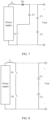
- FIG. 7 is a schematic diagram of a third embodiment of a current path when a direct current-direct current conversion circuit is in a third working state.
- the third switch S3 When the direct current-direct current conversion circuit is in the third working state, the third switch S3 is in a closed state, and the first switch S1 is in a disconnected state.
- a current flows out from the positive electrode of the power supply, and sequentially flows through the input inductor L, the first diode D1, the flying capacitor Cf, and the third switch S3 into the negative electrode of the power supply, and the power supply charges the input inductor L and the flying capacitor Cf.
- a voltage of a connection point between the input inductor L and the first switch S1 is Vf.
- FIG. 8 is a schematic diagram of a fourth embodiment of a current path when a direct current-direct current conversion circuit is in a fourth working state.
- the direct current-direct current conversion circuit When the direct current-direct current conversion circuit is in the fourth working state, the first switch S1 and the third switch S3 are in a closed state, and a current flows out from the positive electrode of the power supply, and sequentially flows through the first switch S1 and the third switch S3 into the negative electrode of the power supply, and the power supply charges the input inductor L.
- a voltage of a connection point between the input inductor L and the first switch S1 is 0.
- the direct current-direct current conversion circuit works sequentially in the second working state, the fourth working state, and the third working state, to implement three-level output.
- the duty cycle D of the control signal is less than 0.5, in a working period, the direct current-direct current conversion circuit works sequentially in the second working state, the first working state, and the third working state, to implement three-level output.
- the negative electrode of the power supply is directly connected to the second capacitor C2 by using a wire, regardless of a change of the working state of the direct current-direct current conversion circuit, a voltage of any position between the negative electrode of the power supply and the second capacitor C2 does not change. To be specific, a common mode voltage does not change. Therefore, no common mode current is generated.
- the reverse recovery process when the first diode D1 is turned off is inhibited by controlling closing time of the first switch S1 and the second switch S2.
- the second inductor Lr2, the fourth switch S4, and the second buffer circuit are added to form the second soft switch unit 200 together with the second switch S2 and the second diode D2.
- the reverse recovery process when the second diode D2 is turned off is inhibited by controlling turn-on time of the third switch S3 and the fourth switch S4.
- the following describes in detail working processes of the first soft switch unit 100 and the second soft switch unit 200.
- the first soft switch unit 100 it is first assumed that the first switch S1 is in a disconnected state, and the first diode D1 is in a turn-on state. Before the first switch S1 is closed, the second switch S2 is first closed. Due to an effect of the first inductor Lr1, a current of the second switch S2 slowly increases starting from zero, to implement zero-current turn-on of the second switch S2. In addition, a current of the first diode D1 slowly decreases, to inhibit the reverse recovery process of the first diode D1. When the current of the first diode D1 decreases to zero, the first diode D1 is turned off.
- the first inductor Lr1 stores energy
- instantaneous current impact is caused to the second switch S2 when the second switch S2 is closed next time. Consequently, the current of the second switch S2 cannot slowly increase starting from zero.
- the current of the first diode D1 cannot slowly decrease. Consequently, an effect of inhibiting reverse recovery of the first diode D1 becomes poor. Therefore, to ensure that reverse recovery of the first diode D1 can be effectively inhibited and zero-current turn-on of the second switch S2 can be implemented each time the second switch S2 is closed, after the second switch S2 is disconnected, the energy of the first inductor Lr1 is transferred by using the first buffer circuit.
- the first buffer circuit transfers the energy of the first inductor Lr1
- the third switch S3 when the third switch S3 is in a closed state, a current flows out from the first buffer circuit, and sequentially flows through the flying capacitor Cf and the third switch S3 into the negative electrode of the power supply.
- the energy of the first inductor Lr1 is transferred to the flying capacitor Cf by the first buffer circuit.
- the third switch S3 When the third switch S3 is in a disconnected state, the current flows out from the first buffer circuit, and sequentially flows through the second diode D2, the first capacitor C1, and the second capacitor C2 into the negative electrode of the power supply. In this process, the energy of the first inductor Lr1 is transferred to the first capacitor C1 and the second capacitor C2 by the first buffer circuit.
- the third switch S3 is in a disconnected state, and the second diode D2 is in a turn-on state.
- the fourth switch S4 is first closed. Due to an effect of the second inductor Lr2, a current of the fourth switch S4 slowly increases starting from zero, to implement zero-current turn-on of the fourth switch S4. In addition, a current of the second diode D2 slowly decreases, to inhibit the reverse recovery process of the second diode D2. When the current of the second diode D2 decreases to zero, the second diode D2 is turned off.
- the second inductor Lr2 also stores energy, to ensure that reverse recovery of the second diode D2 can be effectively inhibited and zero-current turn-on of the fourth switch S4 can be implemented each time the fourth switch S4 is closed, after the fourth switch S4 is disconnected, the energy of the second inductor Lr2 is transferred by using the second buffer circuit.
- the current flows out from the second buffer circuit, and flows through the second capacitor C2 into the negative electrode of the power supply.
- the energy of the second inductor Lr2 is transferred to the second capacitor C2 by the second buffer circuit.
- first buffer circuit there are a plurality of structures of the first buffer circuit and the second buffer circuit.
- FIG. 9 is a schematic diagram of a second embodiment of the direct current-direct current conversion circuit according to an embodiment of this application.
- the first buffer circuit includes a third diode D3, a fourth diode D4, and a third capacitor C3.
- a positive electrode of the third diode D3 is the second terminal 6 of the first buffer circuit, a negative electrode of the third diode D3 is connected to a positive electrode of the fourth diode D4, and a negative electrode of the fourth diode D4 is the third terminal 7 of the first buffer circuit.
- a first terminal of the third capacitor C3 is the first terminal 5 of the first buffer circuit, and a second terminal of the third capacitor C3 is connected between the third diode D3 and the fourth diode D4.
- a working process of the first soft switch unit 100 is as follows:
- the second switch S2 is first closed. A current of the second switch S2 slowly increases starting from zero, to implement zero-current turn-on of the second switch S2. In addition, a current of the first diode D1 slowly decreases, to inhibit the reverse recovery process of the first diode D1. When the current of the first diode D1 decreases to zero, the first diode D1 is turned off. As a current of the first inductor Lr1 constantly increases, a voltage of two terminals of the first switch S1 gradually decreases to zero. In this case, the first switch S1 is closed, to implement zero-voltage turn-on of the first switch S1, and then the second switch S2 is disconnected. In a period in which the second switch S2 is closed, the first buffer circuit does not work, and a voltage of two terminals of the third capacitor C3 is always zero.
- the first inductor Lr1 implements freewheeling by using the third diode D3 and the third capacitor C3.
- the first inductor Lr1 charges the third capacitor C3.
- a voltage of two terminals of the third capacitor C3 constantly increases, and a voltage of a terminal that is of the third capacitor C3 and that is connected to the third diode D3 is a positive voltage, so that the first diode D1 bears a reverse voltage, and finally the energy of the first inductor Lr1 is completely transferred to the third capacitor C3.
- the first switch S1 When the first switch S1 is disconnected, a current flows out from the positive electrode of the power supply, and a specific flow direction is related to a state of the third switch S3. Because the first diode D1 bears the reverse voltage, the first diode D1 is in a turn-off state.
- the third switch S3 When the third switch S3 is in a closed state, a current sequentially flows through the input inductor L, the third capacitor C3, the fourth diode D4, the flying capacitor Cf, and the third switch S3, and finally flows into the negative electrode of the power supply. In this process, the third capacitor C3 charges the flying capacitor Cf.
- parameters of components in the first soft switch unit 100 may be properly set, so that after the third capacitor C3 is charged by the first inductor Lr1, the voltage of the two terminals of the third capacitor C3 is equal to that of the two terminals of the flying capacitor Cf.
- the first switch S1, the third capacitor C3, the fourth diode D4, and the flying capacitor Cf form a loop, it can be learned that, during disconnection, the voltage of the two terminals of the first switch S1 is zero, so that zero-voltage turn-off of the first switch S1 can be implemented.
- the second buffer circuit includes a fifth diode D5, a sixth diode D6, and a fourth capacitor C4.
- a positive electrode of the fifth diode D5 is the second terminal 9 of the second buffer circuit, a negative electrode of the fifth diode D5 is connected to a positive electrode of the sixth diode D6, and a negative electrode of the sixth diode D6 is the third terminal 10 of the second buffer circuit.
- a first terminal of the fourth capacitor C4 is the first terminal 8 of the second buffer circuit, and a second terminal of the fourth capacitor C4 is connected between the fifth diode D5 and the sixth diode D6.
- the fourth switch S4 is first closed. A current of the fourth switch S4 slowly increases starting from zero, to implement zero-current turn-on of the fourth switch S4. In addition, a current of the second diode D2 slowly decreases, to inhibit the reverse recovery process of the second diode D2. When the current of the second diode D2 decreases to zero, the second diode D2 is turned off. As a current of the second inductor Lr2 constantly increases, a voltage of two terminals of the third switch S3 gradually decreases to zero. In this case, the third switch S3 is closed, to implement zero-voltage turn-on of the third switch S3, and then the fourth switch S4 is disconnected. In a period in which the fourth switch S4 is closed, the second buffer circuit does not work, and a voltage of two terminals of the fourth capacitor C4 is always zero.
- the second inductor Lr2 implements freewheeling by using the fifth diode D5 and the fourth capacitor C4.
- the second inductor Lr2 charges the fourth capacitor C4.
- a voltage of two terminals of the fourth capacitor C4 constantly increases, and a voltage of a terminal that is of the fourth capacitor C4 and that is connected to the fifth diode D5 is a positive voltage, so that the second diode D2 bears a reverse voltage, and finally the energy of the second inductor Lr2 is completely transferred to the fourth capacitor C4.
- the fourth capacitor C4 When the first switch S1 is in a disconnected state, a current sequentially flows through the input inductor L, the first diode D1, the flying capacitor Cf, the fourth capacitor C4, the sixth diode D6, and the second capacitor C2, and finally flows into the negative electrode of the power supply. In this process, the fourth capacitor C4 also charges the second capacitor C2. In this way, the energy of the fourth capacitor C4 is transferred to the second capacitor C2, that is, the energy of the second inductor Lr2 is transferred to the second capacitor C2. As the fourth capacitor C4 constantly discharges, the reverse voltage of two terminals of the second diode D2 gradually decreases. When the reverse voltage of the two terminals of the second diode D2 decreases to zero, the second diode D2 is naturally turned on.
- parameters of components in the second soft switch unit 200 may be properly set, so that after the fourth capacitor C4 is charged by the second inductor Lr2, the voltage of the two terminals of the fourth capacitor C4 is equal to that of the two terminals of the second capacitor C2.
- the third switch S3, the fourth capacitor C4, the sixth diode D6, and the second capacitor C2 form a loop, it can be learned that, during disconnection, the voltage of the two terminals of the second switch S2 is zero, so that zero-voltage turn-off of the second switch S2 can be implemented.
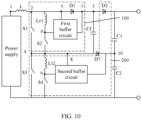
- FIG. 10 is a schematic diagram of a third embodiment of the direct current-direct current conversion circuit according to an embodiment of this application.
- the direct current-direct current conversion circuit further includes a seventh diode D7.
- a positive electrode of the seventh diode D7 is connected to the second terminal 4 of the flying capacitor Cf, and a negative electrode of the seventh diode D7 is connected between the first capacitor C1 and the second capacitor C2.
- the seventh diode D7 may be disposed to limit a voltage of two terminals of the third switch S3 to below a voltage of two terminals of the second capacitor C2, so that the third switch S3 has no risk of overvoltage.
- the second diode D2 can be further prevented from being broken down in a circuit power-on process.
- output terminals of a plurality of direct current-direct current conversion circuits in this embodiment of this application may be used in parallel.
- power-on time of the direct current-direct current conversion circuits may be different. After one of the direct current-direct current conversion circuits is powered on, voltages of two terminals of the first capacitor C1 and the second capacitor C2 in all the direct current-direct current conversion circuits are established as an output voltage Vout, and in a direct current-direct current conversion circuit that is not powered on, the voltage of the two terminals of the flying capacitor Cf is still zero.
- the seventh diode D7 When the seventh diode D7 is not disposed, the moment the power supply is connected and the third switch S3 is closed to charge the flying capacitor Cf, the second diode D2 bears the entire output voltage Vout.
- the third switch S3 may not be closed first, and the flying capacitor Cf is pre-charged by using a closed loop including the positive electrode of the power supply, the input inductor L, the flying capacitor Cf, the seventh diode D7, the second capacitor C2, and the negative electrode of the power supply.
- the voltage of the flying capacitor Cf is equal to the voltage of the two terminals of the first capacitor C1, pre-charging ends, and then the third switch S3 is closed to continue to charge the flying capacitor Cf.
- the voltage born by the second diode D2 is only the voltage of the two terminals of the second capacitor C2, namely, a half of the output voltage Vout. Therefore, the second diode D2 can prevent the second diode D2 from being broken down when bearing the entire output voltage Vout.
- the voltage of the first capacitor C1 is not equal to the voltage of the second capacitor C2, and longer working time indicates a larger difference between the voltages of the first capacitor C1 and the second capacitor C2.
- a capacitance balance circuit is added to two terminals of the first capacitor C1 and the second capacitor C2, for balancing voltages of the first capacitor C1 and the second capacitor C2.
- a first terminal 11 of the capacitance balance circuit is connected to a negative electrode of the second diode D2
- a second terminal 12 of the capacitance balance circuit is connected between the first capacitor C1 and the second capacitor C2
- a third terminal 13 of the capacitance balance circuit is connected to the negative electrode of the power supply.
- FIG. 11 is a schematic diagram of a fourth embodiment of the direct current-direct current conversion circuit according to an embodiment of this application.
- the direct current-direct current conversion circuit further includes an inverter.
- a positive input terminal of the inverter is connected to a negative electrode of the second diode D2, a bus capacitance midpoint of the inverter is connected to a connection point between the first capacitor C1 and the second capacitor C2, and a negative input terminal of the inverter is connected to the negative electrode of the power supply.
- the inverter itself can balance the voltages of the first capacitor C1 and the second capacitor C2. Therefore, when the output terminal of the direct current-direct current conversion circuit is further connected to the inverter, the inverter is equivalent to the capacitance balance circuit.
- the capacitance balance circuit includes a third branch, a fourth branch, and a fifth branch.
- the third branch includes a ninth diode D9, an eighth diode D8, a sixth switch S6, and a fifth switch S5 that are sequentially connected in series, where a negative electrode of the ninth diode D9 is connected to the negative electrode of the second diode D2, a positive electrode of the ninth diode D9 is connected to a negative electrode of the eighth diode D8, a first terminal of the fifth switch S5 is connected to the sixth switch S6, and a second terminal of the fifth switch S5 is connected to the negative electrode of the power supply.
- a first terminal of the fourth branch is connected between the first capacitor C1 and the second capacitor C2, and a second terminal of the fourth branch is connected between the eighth diode D8 and the sixth switch S6.
- a first terminal of the fifth branch is connected between the eighth diode D8 and the ninth diode D9, and a second terminal of the fifth branch is connected between the sixth switch S6 and the fifth switch S5.
- a fifth capacitor C5 is connected in series in the fifth branch.
- a third inductor Lr3 is further connected in series in the fifth branch or the third inductor Lr3 is connected in series in the fourth branch.
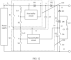
- FIG. 12 is a schematic diagram of a fifth embodiment of a direct current-direct current conversion circuit according to an embodiment of this application.
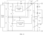
- FIG. 13 is a schematic diagram of a sixth embodiment of a direct current-direct current conversion circuit according to an embodiment of this application.
- the direct current-direct current conversion circuit shown in FIG. 12 differs from the direct current-direct current conversion circuit shown in FIG. 13 merely in that positions of the third inductors Lr3 are different, and other structures and working processes are all the same, the following describes a working process of the capacitance balance circuit by using the direct current-direct current conversion circuit shown in FIG. 12 as an example.
- the fifth capacitor C5 is charged first, until a voltage of two terminals of the fifth capacitor C5 is equal to the voltage of the two terminals of the first capacitor C1 and the voltage of the two terminals of the second capacitor C2.
- the voltage of the two terminals of the second capacitor C2 is higher than the voltage of the two terminals of the first capacitor C1.
- the fifth switch S5 is closed, and the second capacitor C2 charges the fifth capacitor C5, so that the voltage of the two terminals of the second capacitor C2 is reduced. After the voltage of the two terminals of the second capacitor C2 is equal to the voltage of the two terminals of the fifth capacitor C5, charging ends.
- the fifth switch S5 is disconnected and the sixth switch S6 is closed.
- the fifth capacitor C5 charges the first capacitor C1, so that the voltage of the first capacitor C1 increases.
- the foregoing process is constantly performed, to balance the voltages of the first capacitor C1 and the second capacitor C2.
- the third inductor Lr3 implements a buffering function
- the eighth diode D8 and the ninth diode D9 implement a function of limiting a current flow direction.
- the foregoing voltage balance process may be performed periodically.
- the capacitance balance circuit includes a sixth branch, a seventh branch, and an eighth branch.
- the sixth branch includes a tenth switch S10, a ninth switch S9, an eighth switch S8, and a seventh switch S7 that are sequentially connected in series, where a first terminal of the tenth switch S10 is connected to the negative electrode of the second diode D2, a second terminal of the tenth switch S10 is connected to the ninth switch S9, a first terminal of the seventh switch S7 is connected to the eighth switch S8, and a second terminal of the seventh switch S7 is connected to the negative electrode of the power supply.
- a first terminal of the seventh branch is connected between the first capacitor C1 and the second capacitor C2, and a second terminal of the seventh branch is connected between the eighth switch S8 and the ninth switch S9.
- a first terminal of the eighth branch is connected between the ninth switch S9 and the tenth switch S10, and a second terminal of the eighth branch is connected between the seventh switch S7 and the eighth switch S8.
- a sixth capacitor C6 is connected in series in the eighth branch.
- a fourth inductor Lr4 is further connected in series in the eighth branch or the fourth inductor Lr4 is connected in series in the fourth branch.
- FIG. 14 is a schematic diagram of a seventh embodiment of a direct current-direct current conversion circuit according to an embodiment of this application.
- FIG. 15 is a schematic diagram of an eighth embodiment of a direct current-direct current conversion circuit according to an embodiment of this application.
- the direct current-direct current conversion circuit shown in FIG. 14 differs from the direct current-direct current conversion circuit shown in FIG. 15 merely in that positions of the third inductors Lr3 are different, and other structures and working processes are all the same, the following describes a working process of the capacitance balance circuit by using the direct current-direct current conversion circuit shown in FIG. 14 as an example.
- the sixth capacitor C6 is also charged first, until a voltage of two terminals of the sixth capacitor C6 is equal to the voltage of the two terminals of the first capacitor C1 and the voltage of the two terminals of the second capacitor C2.
- the voltage of the two terminals of the second capacitor C2 is higher than the voltage of the two terminals of the first capacitor C1.
- the ninth switch S9 and the seventh switch S7 are closed, and the second capacitor C2 charges the sixth capacitor C6, so that the voltage of the second capacitor C2 is reduced.
- the fourth inductor Lr4 implements a buffering function in the foregoing process.
- the foregoing voltage balance process may be performed periodically.
- the direct current-direct current conversion circuit shown in FIG. 3 is an active direct current-direct current conversion circuit.
- the foregoing describes the active direct current-direct current conversion circuit.
- the following describes in detail a passive direct current-direct current conversion circuit including passive soft switch units.
- FIG. 16 is a schematic diagram of a ninth embodiment of a direct current-direct current conversion circuit according to an embodiment of this application.
- An embodiment of this application provides an embodiment of the direct current-direct current conversion circuit, including: an input inductor L, a first capacitor C1, a second capacitor C2, a flying capacitor Cf, a first soft switch unit 300, and a second soft switch unit 400.
- the first soft switch unit 300 includes a first switch S1, a first inductor Lr1, a first diode D1, and a first buffer circuit
- the second soft switch unit 400 includes a second switch S2, a second inductor Lr2, a second diode D2, and a second buffer circuit.
- the first switch S1 and the second switch S2 may be a metal-oxide semiconductor field effect transistor or an insulated gate bipolar transistor.
- a power supply, the input inductor L, the first diode D1, the second diode D2, the first capacitor C1, and the second capacitor C2 are sequentially connected in series, where a first terminal 1 of the input inductor L is connected to a positive electrode of the power supply, a second terminal 2 of the input inductor L is connected to a positive electrode of the first diode D1, and a negative electrode of the first diode D1 is connected to a positive electrode of the second diode D2.
- the power supply may be any circuit module that can output a current.
- the power supply may be a photovoltaic module.
- a first branch is connected in parallel between the second terminal 2 of the input inductor L and a negative electrode of the power supply, the first branch includes the first inductor Lr1, the first switch S1, the second inductor Lr2, and the second switch S2 that are sequentially connected in series, and the first inductor Lr1 is connected to the second terminal 2 of the input inductor L. As shown in FIG. 16 , the second switch S2 is connected to the negative electrode of the power supply.
- a first terminal 3 of the flying capacitor Cf is connected between the first diode D1 and the second diode D2, and a second terminal 4 of the flying capacitor Cf is connected between the first switch S1 and the second inductor Lr2.
- a first terminal 5 of the first buffer circuit is connected to the positive electrode of the first diode D1
- a second terminal 6 of the first buffer circuit is connected between the first inductor Lr1 and the first switch S1
- a third terminal 7 of the first buffer circuit is connected to the negative electrode of the first diode D1
- a fourth terminal 8 of the first buffer circuit is connected to the second terminal 4 of the flying capacitor Cf.
- the first buffer circuit is configured to transfer energy of the first inductor Lr1 to the flying capacitor Cf, or to the first capacitor C1 and the second capacitor C2.
- a first terminal 9 of the second buffer circuit is connected to the second terminal 4 of the flying capacitor Cf, a second terminal 10 of the second buffer circuit is connected between the second inductor Lr2 and the second switch S2, a third terminal 11 of the second buffer circuit is connected between the first capacitor C1 and the second capacitor C2, and a fourth terminal 12 of the second buffer circuit is connected to the negative electrode of the power supply.
- the second buffer circuit is configured to transfer energy of the second inductor Lr2 to the second capacitor C2.
- the following analyzes working states of the direct current-direct current conversion circuit in this embodiment of this application based on the foregoing circuit structure.
- the input inductor L, the first capacitor C1, the second capacitor C2, and the flying capacitor Cf are all sufficiently large, to ensure that in a working process of the direct current-direct current conversion circuit, a voltage Vf of two terminals of the flying capacitor Cf and output voltages Vout of two terminals of the first capacitor C1 and of two terminals of the second capacitor C2 remain basically unchanged.
- the input inductor L, the first switch S1, the second switch S2, the first diode D1, the second diode D2, the flying capacitor Cf, the first capacitor C1, and the second capacitor C2 may constitute the flying capacitor Cf based boost chopper circuit shown in FIG. 17 . It can be learned based on a working principle of the flying capacitor Cf based boost chopper circuit that, when the boost chopper circuit shown in FIG. 17 works normally, an output voltage Vout is greater than a power supply voltage Vin, and voltages of the first capacitor C1 and the second capacitor C2 always remain the same. In addition, switching states of the first switch S1 and the second switch S2 are changed by using a control signal, so that the direct current-direct current conversion circuit in this embodiment of this application can work in the following four working states.
- a schematic diagram of a current path is the same as that shown in FIG. 5 .
- the first switch S1 and the second switch S2 are in a disconnected state, and a current flows out from the positive electrode of the power supply, and sequentially flows through the input inductor L, the first diode D1, the second diode D2, the first capacitor C1, and the second capacitor C2 into the negative electrode of the power supply, and the input inductor L charges the first capacitor C1 and the second capacitor C2.
- a voltage of a connection point between the input inductor L and the first switch S1 is Vout.
- FIG. 18 is a schematic diagram of a fifth embodiment of a current path when a direct current-direct current conversion circuit is in a second working state.
- the direct current-direct current conversion circuit When the direct current-direct current conversion circuit is in the second working state, the first switch S1 is in a closed state, and the second switch S2 is in a disconnected state.
- a current flows out from the positive electrode of the power supply, and sequentially flows through the input inductor L, the first switch S1, the flying capacitor Cf, the second diode D2, the first capacitor C1, and the second capacitor C2 into the negative electrode of the power supply, and the input inductor L and the flying capacitor Cf jointly charge the first capacitor C1 and the second capacitor C2.
- a voltage of a connection point between the input inductor L and the first switch S1 is Vout-Vf.
- FIG. 19 is a schematic diagram of a sixth embodiment of a current path when a direct current-direct current conversion circuit is in a third working state.
- the direct current-direct current conversion circuit is in the third working state, the second switch S2 is in a closed state, and the first switch S1 is in a disconnected state.
- a current flows out from the positive electrode of the power supply, and sequentially flows through the input inductor L, the first diode D1, the flying capacitor Cf, and the second switch S2 into the negative electrode of the power supply, and the power supply charges the input inductor L and the flying capacitor Cf.
- a voltage of a connection point between the input inductor L and the first switch S1 is Vf.
- FIG. 20 is a schematic diagram of a seventh embodiment of a current path when a direct current-direct current conversion circuit is in a fourth working state.
- the direct current-direct current conversion circuit When the direct current-direct current conversion circuit is in the fourth working state, the first switch S1 and the second switch S2 are in a closed state. A current flows out from the positive electrode of the power supply, and sequentially flows through the first switch S1 and the second switch S2 into the negative electrode of the power supply, and the power supply charges the input inductor L. A voltage of a connection point between the input inductor L and the first switch S1 is 0.
- the direct current-direct current conversion circuit works sequentially in the second working state, the fourth working state, and the third working state, to implement three-level output.
- the duty cycle D of the control signal is less than 0.5, in a working period, the direct current-direct current conversion circuit works sequentially in the second working state, the first working state, and the third working state, to implement three-level output.
- the negative electrode of the power supply is directly connected to the second capacitor C2 by using a wire, regardless of a change of the working state of the direct current-direct current conversion circuit, a voltage of any position between the negative electrode of the power supply and the second capacitor C2 does not change. To be specific, a common mode voltage does not change. Therefore, no common mode current is generated.
- the second inductor Lr2 and the second buffer circuit are added to form the second soft switch unit 400 together with the second switch S2 and the second diode D2, to inhibit the reverse recovery process when the second diode D2 is turned off.
- the following describes in detail working processes of the first soft switch unit 300 and the second soft switch unit 400.
- the first soft switch unit 300 it is first assumed that the first switch S1 is in a disconnected state, and the first diode D1 is in a turn-on state. Then the first switch S1 is closed. Due to an effect of the first inductor Lr1, a current of the first switch S1 slowly increases starting from zero, to implement zero-current turn-on of the first switch S1. In addition, a current of the first diode D1 slowly decreases, to inhibit the reverse recovery process of the first diode D1. When the current of the first diode D1 decreases to zero, the first diode D1 is turned off.
- the first inductor Lr1 stores energy, if the energy in the first inductor Lr1 is not transferred, instantaneous current impact is caused to the first switch S1 when the first switch S1 is closed next time. Consequently, the current of the first switch S1 cannot slowly increase starting from zero. In addition, the current of the first diode D1 cannot slowly decrease. Consequently, an effect of inhibiting reverse recovery of the first diode D1 becomes poor. Therefore, to ensure that reverse recovery of the first diode D1 can be effectively inhibited each time the first switch S1 is closed, after the first switch S1 is disconnected, the energy of the first inductor Lr1 is transferred by using the first buffer circuit.
- the first buffer circuit transfers the energy of the first inductor Lr1
- the second switch S2 when the second switch S2 is in a closed state, a current flows out from the first buffer circuit, and sequentially flows through the flying capacitor Cf and the second switch S2 into the negative electrode of the power supply.
- the energy of the first inductor Lr1 is transferred to the flying capacitor Cf by the first buffer circuit.
- the second switch S2 When the second switch S2 is in a disconnected state, the current flows out from the first buffer circuit, and sequentially flows through the second diode D2, the first capacitor C1, and the second capacitor C2 into the negative electrode of the power supply. In this process, the energy of the first inductor Lr1 is transferred to the first capacitor C1 and the second capacitor C2 by the first buffer circuit.
- the second soft switch unit 400 it is first assumed that the second switch S2 is in a disconnected state, and the second diode D2 is in a turn-on state. Then, the second switch S2 is closed. Due to an effect of the second inductor Lr2, a current of the second switch S2 slowly increases starting from zero, to implement zero-current turn-on of the second switch S2. In addition, a current of the second diode D2 slowly decreases, to inhibit the reverse recovery process of the second diode D2. When the current of the second diode D2 decreases to zero, the second diode D2 is turned off.
- the second inductor Lr2 also stores energy, based on a reason the same as that of the first soft switch unit 300, to ensure that reverse recovery of the second diode D2 can be effectively inhibited each time the second switch S2 is closed, after the second switch S2 is disconnected, the energy of the second inductor Lr2 is transferred by using the second buffer circuit. Specifically, in a process in which the second buffer circuit transfers the energy of the second inductor Lr2, the current flows out from the second buffer circuit, and may flow through the second capacitor C2 into the negative electrode of the power supply. In this process, the energy of the second inductor Lr2 is transferred to the second capacitor C2 by the second buffer circuit.
- first buffer circuit there are a plurality of structures of the first buffer circuit and the second buffer circuit.
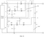
- FIG. 21 is a schematic diagram of a tenth embodiment of the direct current-direct current conversion circuit according to an embodiment of this application.
- the first buffer circuit includes a third diode D3, a fourth diode D4, a fifth diode D5, a third capacitor C3, and a fourth capacitor C4.
- a positive electrode of the third diode D3 is the second terminal 6 of the first buffer circuit, and a negative electrode of the third diode D3 is connected to a positive electrode of the fourth diode D4.
- a negative electrode of the fourth diode D4 is connected to a positive electrode of the fifth diode D5, and a negative electrode of the fifth diode D5 is the third terminal 7 of the first buffer circuit.
- a first terminal of the third capacitor C3 is the first terminal 5 of the first buffer circuit, and a second terminal of the third capacitor C3 is connected between the fourth diode D4 and the fifth diode D5.
- a first terminal of the fourth capacitor C4 is connected between the third diode D3 and the fourth diode D4, and a second terminal of the fourth capacitor C4 is the fourth terminal 8 of the first buffer circuit.
- a working process of the first soft switch unit 300 is as follows:
- the voltage of the two terminals of the fourth capacitor C4 is equal to the voltage of the two terminals of the flying capacitor Cf, and a voltage that is of a terminal of the fourth capacitor C4 and that is connected to the flying capacitor Cf is a negative voltage.
- the first switch S1 is closed, and a current of the first switch S1 slowly increases starting from zero, to implement zero-current turn-on of the first switch S1.
- a current of the first diode D1 slowly decreases, to inhibit the reverse recovery process of the first diode D1.
- the first diode D1 When the current of the first diode D1 decreases to zero, the first diode D1 is turned off. After the first switch S1 is closed, a current flows out from the positive electrode of the power supply, and flows through the input inductor L, the first inductor Lr1, and the first switch S1 to the flying capacitor Cf. In addition, a closed loop including the first inductor Lr1, the first switch S1, the fourth capacitor C4, the fourth diode D4, and the third capacitor C3 starts to resonate for the first time. The fourth capacitor C4 charges the third capacitor C3 and the first inductor Lr1. After the voltage of the two terminals of the fourth capacitor C4 decreases to zero, the third diode D3 is naturally turned on, and the first resonance ends.
- the voltage of the two terminals of the fourth capacitor C4 remains zero, and a closed loop including the first inductor Lr1, the third diode D3, the fourth diode D4, and the third capacitor C3 starts to resonate for the second time.
- the first inductor Lr1 charges the third capacitor C3.
- the third diode D3 and the fourth diode D4 are naturally turned off.
- the voltage of the two terminals of the third capacitor C3 remains unchanged.
- the first diode D1 bears a reverse voltage.
- the first inductor Lr1 implements freewheeling by using the third diode D3.
- a current sequentially flows through the first inductor Lr1, the third diode D3, and the fourth capacitor C4 to the flying capacitor Cf.
- the first inductor Lr1 charges the fourth capacitor C4. Because the voltage of the two terminals of the fourth capacitor C4 constantly increases starting from zero, zero-voltage turn-off of the first switch S1 is implemented. After the voltage of the two terminals of the fourth capacitor C4 increases to be equal to the voltage of the two terminals of the flying capacitor Cf, the fourth diode D4 and the fifth diode D5 are naturally turned on.
- a specific flow direction is related to a state of the second switch S2.
- a current sequentially flows through the flying capacitor Cf and the second switch S2, and finally flows into the negative electrode of the power supply.
- the third capacitor C3 and the first inductor Lr1 charge the flying capacitor Cf. In this way, energy of the first inductor Lr1 and the third capacitor C3 is transferred to the flying capacitor Cf.
- a current sequentially flows through the second diode D2, the first capacitor C1, and the second capacitor C2, and finally flows into the negative electrode of the power supply.
- the third capacitor C3 and the first inductor Lr1 charge the first capacitor C1 and the second capacitor C2. In this way, the energy of the first inductor Lr1 and the third capacitor C3 is transferred to the first capacitor C1 and the second capacitor C2.
- the reverse voltage of two terminals of the first diode D1 gradually decreases.
- the reverse voltage of the two terminals of the first diode D1 decreases to zero, the first diode D1 is naturally turned on. After the first inductor Lr1 finishes charging, the first diode D1 is completely turned on.
- FIG. 21 is a schematic diagram of a tenth embodiment of the direct current-direct current conversion circuit according to an embodiment of this application.
- the second buffer circuit includes a sixth diode D6, an eighth diode D8, a ninth diode D9, a fifth capacitor C5, and a sixth capacitor C6.
- a positive electrode of the sixth diode D6 is the second terminal 10 of the second buffer circuit, and a negative electrode of the sixth diode D6 is connected to a positive electrode of the eighth diode D8.
- a negative electrode of the eighth diode D8 is connected to a positive electrode of the ninth diode D9, and a negative electrode of the ninth diode D9 is the third terminal 11 of the second buffer circuit.
- a first terminal of the fifth capacitor C5 is the first terminal 9 of the second buffer circuit, and a second terminal of the fifth capacitor C5 is connected between the eighth diode D8 and the ninth diode D9.
- a first terminal of the sixth capacitor C6 is connected between the sixth diode D6 and the eighth diode D8, and a second terminal of the sixth capacitor C6 is the fourth terminal 12 of the second buffer circuit.
- the voltage of the two terminals of the sixth capacitor C6 is equal to the voltage of the two terminals of the flying capacitor Cf, and a voltage that is of a terminal of the sixth capacitor C6 and that is connected to the negative electrode of the power supply is a negative voltage.
- the second switch S2 is closed, and a current of the second switch S2 slowly increases starting from zero, to implement zero-current turn-on of the second switch S2.
- a current of the second diode D2 slowly decreases, to inhibit the reverse recovery process of the second diode D2.
- the second diode D2 When the current of the second diode D2 decreases to zero, the second diode D2 is turned off. After the second switch S2 is closed, a current flows through the second inductor Lr2 and the second switch S2 to the negative electrode of the power supply. In addition, a closed loop including the second inductor Lr2, the second switch S2, the sixth capacitor C6, the eighth diode D8, and the fifth capacitor C5 starts to resonate for the first time. The sixth capacitor C6 discharges to the fifth capacitor C5 and the second inductor Lr2. After the voltage of the two terminals of the sixth capacitor C6 decreases to zero, the sixth diode D6 is naturally turned on, and the first resonance ends.
- the voltage of the two terminals of the sixth capacitor C6 remains zero, and a closed loop including the first inductor Lr1, the sixth diode D6, the eighth diode D8, and the fifth capacitor C5 starts to resonate for the second time.
- the second inductor Lr2 charges the fifth capacitor C5. After a current of the fifth capacitor C5 is zero, the second resonance ends.
- the sixth diode D6 and the eighth diode D8 are naturally turned off.
- the voltage of the two terminals of the fifth capacitor C5 remains unchanged.
- the second diode D2 bears a reverse voltage.
- the second inductor Lr2 implements freewheeling by using the sixth diode D6.
- a current sequentially flows through the second inductor Lr2, the sixth diode D6, and the sixth capacitor C6 to the negative electrode of the power supply.
- the second inductor Lr2 charges the sixth capacitor C6. Because the voltage of the two terminals of the sixth capacitor C6 constantly increases starting from zero, zero-voltage turn-off of the second switch S2 is implemented. After the voltage of the two terminals of the sixth capacitor C6 increases to be equal to the voltage of the two terminals of the second capacitor C2, the eighth diode D8 and the ninth diode D9 are naturally turned on.
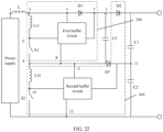
- FIG. 22 is a schematic diagram of an eleventh embodiment of the direct current-direct current conversion circuit according to an embodiment of this application.
- the direct current-direct current conversion circuit further includes a seventh diode D7.
- a positive electrode of the seventh diode D7 is connected to the second terminal 4 of the flying capacitor Cf, and a negative electrode of the seventh diode D7 is connected between the first capacitor C1 and the second capacitor C2.
- the seventh diode D7 may be disposed to limit a voltage of two terminals of the second switch S2 to below a voltage of two terminals of the second capacitor C2, so that the second switch S2 has no risk of overvoltage.
- the second diode D2 can be further prevented from being broken down in a circuit power-on process.
- the voltage of the first capacitor C1 is not equal to the voltage of the second capacitor C2, and longer working time indicates a larger difference between the voltages of the first capacitor C1 and the second capacitor C2.
- a capacitance balance circuit is added to two terminals of the first capacitor C1 and the second capacitor C2, for balancing voltages of the first capacitor C1 and the second capacitor C2.
- a first terminal 13 of the capacitance balance circuit is connected to a negative electrode of the second diode D2
- a second terminal 14 of the capacitance balance circuit is connected between the first capacitor C1 and the second capacitor C2
- a third terminal 15 of the capacitance balance circuit is connected to the negative electrode of the power supply.
- FIG. 23 is a schematic diagram of a twelfth embodiment of the direct current-direct current conversion circuit according to an embodiment of this application.
- the direct current-direct current conversion circuit further includes an inverter.
- a positive input terminal of the inverter is connected to a negative electrode of the second diode D2, a bus capacitance midpoint of the inverter is connected to a connection point between the first capacitor C1 and the second capacitor C2, and a negative input terminal of the inverter is connected to the negative electrode of the power supply.
- the inverter itself can balance the voltages of the first capacitor C1 and the second capacitor C2. Therefore, when the output terminal of the direct current-direct current conversion circuit is further connected to the inverter, the inverter is equivalent to the capacitance balance circuit.
- the capacitance balance circuit includes a second branch, a third branch, and a fourth branch.
- the second branch includes an eleventh diode D11, a tenth diode D10, a fourth switch S4, and a third switch S3 that are sequentially connected in series, where a negative electrode of the eleventh diode D11 is connected to the negative electrode of the second diode D2, a positive electrode of the eleventh diode D11 is connected to a positive electrode of the tenth diode D10, a first terminal of the third switch S3 is connected to the fourth switch S4, and a second terminal of the third switch S3 is connected to the negative electrode of the power supply.
- a first terminal of the third branch is connected between the first capacitor C1 and the second capacitor C2, and a second terminal of the third branch is connected between the tenth diode D10 and the fourth switch S4.
- a first terminal of the fourth branch is connected between the tenth diode D10 and the eleventh diode D11, and a second terminal of the fourth branch is connected between the fourth switch S4 and the third switch S3.
- a seventh capacitor C7 is connected in series in the fourth branch.
- a third inductor Lr3 is further connected in series in the fourth branch or the third inductor Lr3 is connected in series in the third branch.
- FIG. 24 is a schematic diagram of a thirteenth embodiment of a direct current-direct current conversion circuit according to an embodiment of this application.
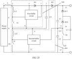
- FIG. 25 is a schematic diagram of a fourteenth embodiment of a direct current-direct current conversion circuit according to an embodiment of this application.
- FIG. 24 and FIG. 25 are respectively the same as those in FIG. 12 and FIG. 13 . Therefore, refer to related descriptions of the capacitance balance circuits shown in FIG. 12 and FIG. 13 in the foregoing embodiments. Details are not described herein.
- the capacitance balance circuit includes a fifth branch, a sixth branch, and a seventh branch.
- the fifth branch includes an eighth switch S8, a seventh switch S7, a sixth switch S6, and a fifth switch S5 that are sequentially connected in series, where a first terminal of the eighth switch S8 is connected to the negative electrode of the second diode D2, a second terminal of the eighth switch S8 is connected to the seventh switch S7, a first terminal of the fifth switch S5 is connected to the sixth switch S6, and a second terminal of the fifth switch S5 is connected to the negative electrode of the power supply.
- a first terminal of the sixth branch is connected between the first capacitor C1 and the second capacitor C2, and a second terminal of the sixth branch is connected between the sixth switch S6 and the seventh switch S7.
- a first terminal of the seventh branch is connected between the seventh switch S7 and the eighth switch S8, and a second terminal of the seventh branch is connected between the fifth switch S5 and the sixth switch S6.
- An eighth capacitor C8 is connected in series in the seventh branch.
- a fourth inductor Lr4 is further connected in series in the seventh branch or the fourth inductor Lr4 is connected in series in the third branch.
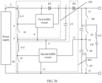
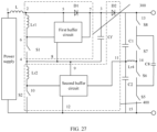
- FIG. 26 is a schematic diagram of a fifteenth embodiment of a direct current-direct current conversion circuit according to an embodiment of this application.
- FIG. 27 is a schematic diagram of a sixteenth embodiment of a direct current-direct current conversion circuit according to an embodiment of this application.
- FIG. 26 and FIG. 27 are respectively the same as those in FIG. 14 and FIG. 15 . Therefore, refer to related descriptions of the capacitance balance circuits shown in FIG. 14 and FIG. 15 in the foregoing embodiments. Details are not described herein.
- the program may be stored in a computer-readable storage medium.
- the storage medium may include: any medium that can store program code, such as a USB flash drive, a removable hard disk, a read-only memory (read-only memory, ROM), a random access memory (random access memory, RAM), a magnetic disk, or an optical disc.
Landscapes
- Engineering & Computer Science (AREA)
- Power Engineering (AREA)
- Dc-Dc Converters (AREA)
Claims (6)
- Gleichstrom-Gleichstrom-Umwandlungsschaltung, die umfasst: eine Eingangsinduktivität (L), einen ersten Kondensator (C1), einen zweiten Kondensator (C2), einen Flying Capacitor (Cf), einen ersten Schalter (S1), einen zweiten Schalter (S2), eine erste Induktivität (Lr1), eine erste Diode (D1), eine erste Pufferschaltung, einen dritten Schalter (S3), einen vierten Schalter (S4), eine zweite Induktivität (Lr2), eine zweite Diode (D2) und eine zweite Pufferschaltung, wobeidie Gleichstrom-Gleichstrom-Umwandlungsschaltung konfiguriert ist, um mit einer Leistungsversorgung derart verbindbar zu sein, dass die Leistungsversorgung, die Eingangsinduktivität (L), die erste Diode (D1), die zweite Diode (D2), der erste Kondensator (C1) und der zweite Kondensator (C2) in Reihe verbunden sind, wobei ein erster Anschluss der Eingangsinduktivität (L) mit einer positiven Elektrode der Leistungsversorgung verbunden ist, ein zweiter Anschluss der Eingangsinduktivität (L) mit einer positiven Elektrode der ersten Diode (D1) verbunden ist und eine negative Elektrode der ersten Diode (D1) mit einer positiven Elektrode der zweiten Diode (D2) verbunden ist und der zweite Kondensator (C2) mit einer negativen Elektrode der Leistungsversorgung verbunden ist und die Spannung über dem ersten Kondensator (C1) und dem zweiten Kondensator (C2) die Ausgangsspannung der Gleichstrom-Gleichstrom-Umwandlungsschaltung ist;ein erster Zweig und ein zweiter Zweig zwischen dem zweiten Anschluss der Eingangsinduktivität (L) und der negativen Elektrode der Leistungsversorgung parallel verbunden sind, der erste Zweig den ersten Schalter (S1) und den dritten Schalter (S3), die in Reihe verbunden sind, umfasst, der zweite Zweig die erste Induktivität (Lr1), den zweiten Schalter (S2), die zweite Induktivität (Lr2) und den vierten Schalter (S4), die in Reihe verbunden sind, umfasst und der erste Schalter (S1) und die erste Induktivität (Lr1) beide mit dem zweiten Anschluss der Eingangsinduktivität (L) verbunden sind;ein erster Anschluss des Flying Capacitor (Cf) mit einem Knoten zwischen der ersten Diode (D1) und der zweiten Diode (D2) verbunden ist, ein zweiter Anschluss des Flying Capacitor (Cf) mit einem Knoten zwischen dem ersten Schalter (S1) und dem dritten Schalter (S3) verbunden ist;die erste Pufferschaltung mindestens eine dritte Diode (D3), eine vierte Diode (D4) und einen dritten Kondensator (C3), der konfiguriert ist, um Energie zu speichern, umfasst, die dritte Diode und die vierte Diode in Reihe verbunden sind, die positive Elektrode der dritten Diode mit einem Knoten zwischen der ersten Induktivität und dem zweiten Schalter verbunden ist, ein erster Anschluss des dritten Kondensators mit der positiven Elektrode der ersten Diode (D1) verbunden ist, ein zweiter Anschluss des dritten Kondensators mit der negativen Elektrode der dritten Diode verbunden ist und der zweite Anschluss des dritten Kondensators durch die vierte Diode mit der negativen Elektrode der ersten Diode (D1) verbunden ist;der zweite Puffer mindestens eine fünfte Diode (D5), eine sechste Diode (D6) und einen vierten Kondensator (C4), der konfiguriert ist, um Energie zu speichern, umfasst, wobei die fünfte Diode und die sechste Diode in Reihe verbunden sind, die positive Elektrode der fünften Diode mit einem Knoten zwischen der zweiten Induktivität und dem vierten Schalter verbunden ist, ein erster Anschluss des vierten Kondensators mit dem zweiten Anschluss des Flying Capacitor (Cf) verbunden ist, ein zweiter Anschluss des vierten Kondensators mit der negativen Elektrode der fünften Diode verbunden ist und der zweite Anschluss des vierten Kondensators durch die sechste Diode mit einem Knoten zwischen dem ersten Kondensator (C1) und dem zweiten Kondensator (C2) verbunden ist;wobei die Umwandlungsschaltung derart konfiguriert ist, dass, wenn die Leistungsversorgung mit der Schaltung verbunden wird, die folgenden Schritte durchgeführt werden können:wenn der zweite Schalter (S2) in einem geschlossenen Zustand ist, speichert die erste Induktivität (Lr1) Energie,wenn der zweite Schalter (S2) in einem getrennten Zustand ist, lädt die erste Induktivität (Lr1) den dritten Kondensator derart, dass die erste Diode (D1) eine Sperrspannung trägt, und, wenn der dritte Schalter (S3) in einem geschlossenen Zustand ist, übertragen die erste Induktivität und der dritte Kondensator Energie auf den Flying Capacitor (Cf) oder, wenn der dritte Schalter (S3) in einem getrennten Zustand ist, überträgt der dritte Kondensator Energie mittels der zweiten Diode (D2) auf den ersten Kondensator (C1) und den zweiten Kondensator (C2); undwenn der vierte Schalter (S4) in einem geschlossenen Zustand ist, speichert der zweite Induktor (Lr2) Energie, wenn der vierte Schalter (S4) in einem getrennten Zustand ist, lädt die zweite Induktivität (Lr2) den vierten Kondensator derart, dass die zweite Diode (D2) eine Sperrspannung trägt, und der vierte Kondensator überträgt Energie auf den zweiten Kondensator (C2).
- Gleichstrom-Gleichstrom-Umwandlungsschaltung nach Anspruch 1, die ferner eine siebte Diode (D7) umfasst, wobei
eine positive Elektrode der siebten Diode (D7) mit dem zweiten Anschluss des Flying Capacitor (Cf) verbunden ist und eine negative Elektrode der siebten Diode (D7) zwischen dem ersten Kondensator (C1) und dem zweiten Kondensator (C2) verbunden ist. - Gleichstrom-Gleichstrom-Umwandlungsschaltung nach Anspruch 1 oder 2, die ferner eine Kapazitätsausgleichsschaltung umfasst, wobeiein erster Anschluss der Kapazitätsausgleichsschaltung mit einer negativen Elektrode der zweiten Diode (D2) verbunden ist, ein zweiter Anschluss der Kapazitätsausgleichsschaltung zwischen dem ersten Kondensator (C1) und dem zweiten Kondensator (C2) verbunden ist und ein dritter Anschluss der Kapazitätsausgleichsschaltung mit der negativen Elektrode der Leistungsversorgung verbunden ist; unddie Kapazitätsausgleichsschaltung konfiguriert ist, um Spannungen des ersten Kondensators (C1) und des zweiten Kondensators (C2) auszugleichen.
- Gleichstrom-Gleichstrom-Umwandlungsschaltung nach einem der Ansprüche 1 bis 3, die ferner einen Wechselrichter umfasst, wobei
ein positiver Eingangsanschluss des Wechselrichters mit einer negativen Elektrode der zweiten Diode (D2) verbunden ist, ein Buskapazitätsmittelpunkt des Wechselrichters mit einem Verbindungspunkt zwischen dem ersten Kondensator (C1) und dem zweiten Kondensator (C2) verbunden ist und ein negativer Eingangsanschluss des Wechselrichters mit der negativen Elektrode der Leistungsversorgung verbunden ist. - Gleichstrom-Gleichstrom-Umwandlungsschaltung nach Anspruch 3, wobei die Kapazitätsausgleichsschaltung einen dritten Zweig, einen vierten Zweig und einen fünften Zweig umfasst, wobeider dritte Zweig eine neunte Diode (D9), eine achte Diode (D8), einen sechsten Schalter (S6) und einen fünften Schalter (S5), die nacheinander in Reihe verbunden sind, umfasst, wobei eine negative Elektrode der neunten Diode (D9) mit der negativen Elektrode der zweiten Diode (D2) verbunden ist, eine positive Elektrode der neunten Diode (D9) mit einer negativen Elektrode der achten Diode (D8) verbunden ist, ein erster Anschluss des fünften Schalters (S5) mit dem sechsten Schalter (S6) verbunden ist und ein zweiter Anschluss des fünften Schalters (S5) mit der negativen Elektrode der Leistungsversorgung verbunden ist;ein erster Anschluss des vierten Zweigs zwischen dem ersten Kondensator (C1) und dem zweiten Kondensator (C2) verbunden ist und ein zweiter Anschluss des vierten Zweigs zwischen der achten Diode (D8) und dem sechsten Schalter (S6) verbunden ist;ein erster Anschluss des fünften Zweigs zwischen der achten Diode (D8) und der neunten Diode (D9) verbunden ist und ein zweiter Anschluss des fünften Zweigs zwischen dem sechsten Schalter (S6) und dem fünften Schalter (S5) verbunden ist;ein fünfter Kondensator (C5) in dem fünften Zweig in Reihe verbunden ist; und eine dritte Induktivität (Lr3) ferner in dem fünften Zweig in Reihe verbunden ist oder die dritte Induktivität (Lr3) in dem vierten Zweig in Reihe verbunden ist.
- Gleichstrom-Gleichstrom-Umwandlungsschaltung nach Anspruch 3, wobei die Kapazitätsausgleichsschaltung einen sechsten Zweig, einen siebten Zweig und einen achten Zweig umfasst, wobeider sechste Zweig einen zehnten Schalter (S10), einen neunten Schalter (S9), einen achten Schalter (S8) und einen siebten Schalter (S7), die nacheinander in Reihe verbunden sind, umfasst, wobei ein erster Anschluss des zehnten Schalters (S10) mit der negativen Elektrode der zweiten Diode (D2) verbunden ist, ein zweiter Anschluss des zehnten Schalters (S10) mit dem neunten Schalter (S9) verbunden ist, ein erster Anschluss des siebten Schalters (S7) mit dem achten Schalter (S8) verbunden ist und ein zweiter Anschluss des siebten Schalters (S7) mit der negativen Elektrode der Leistungsversorgung verbunden ist;ein erster Anschluss des siebten Zweigs zwischen dem ersten Kondensator (C1) und dem zweiten Kondensator (C2) verbunden ist und ein zweiter Anschluss des siebten Zweigs zwischen dem achten Schalter (S8) und dem neunten Schalter (S9) verbunden ist;ein erster Anschluss des achten Zweigs zwischen dem neunten Schalter (S9) und dem zehnten Schalter (S10) verbunden ist und ein zweiter Anschluss des achten Zweigs zwischen dem siebten Schalter (S7) und dem achten Schalter (S8) verbunden ist;ein sechster Kondensator (C6) in dem achten Zweig in Reihe verbunden ist; und eine vierte Induktivität (Lr4) in dem achten Zweig in Reihe verbunden ist oder die vierte Induktivität (Lr4) in dem vierten Zweig in Reihe verbunden ist.
Applications Claiming Priority (2)
| Application Number | Priority Date | Filing Date | Title |
|---|---|---|---|
| CN201910754932.8A CN110649810B (zh) | 2019-08-15 | 2019-08-15 | 一种直流-直流变换电路 |
| PCT/CN2020/101898 WO2021027468A1 (zh) | 2019-08-15 | 2020-07-14 | 一种直流-直流变换电路 |
Publications (3)
| Publication Number | Publication Date |
|---|---|
| EP4016828A1 EP4016828A1 (de) | 2022-06-22 |
| EP4016828A4 EP4016828A4 (de) | 2022-09-28 |
| EP4016828B1 true EP4016828B1 (de) | 2025-05-21 |
Family
ID=69009595
Family Applications (1)
| Application Number | Title | Priority Date | Filing Date |
|---|---|---|---|
| EP20851876.1A Active EP4016828B1 (de) | 2019-08-15 | 2020-07-14 | Gleichspannungswandlerschaltung |
Country Status (4)
| Country | Link |
|---|---|
| US (1) | US11894762B2 (de) |
| EP (1) | EP4016828B1 (de) |
| CN (1) | CN110649810B (de) |
| WO (1) | WO2021027468A1 (de) |
Families Citing this family (6)
| Publication number | Priority date | Publication date | Assignee | Title |
|---|---|---|---|---|
| WO2020259801A1 (en) * | 2019-06-25 | 2020-12-30 | Huawei Technologies Co., Ltd. | A dc-to-dc power converter |
| CN110649810B (zh) | 2019-08-15 | 2021-09-14 | 华为技术有限公司 | 一种直流-直流变换电路 |
| CN111654183B (zh) * | 2020-06-12 | 2021-10-29 | 深圳英飞源技术有限公司 | 一种直流-直流变换装置及其控制方法 |
| CN111873802B (zh) * | 2020-07-23 | 2022-03-04 | 蜂巢能源科技有限公司 | 确定电子器件的方法、装置、介质及设备 |
| CN114678917B (zh) * | 2021-04-27 | 2026-04-24 | 北京新能源汽车股份有限公司 | 一种快充保护电路及车辆 |
| CN115001264B (zh) * | 2022-06-07 | 2024-09-10 | 漳州科华电气技术有限公司 | 直流变换电路、控制方法及控制终端 |
Citations (2)
| Publication number | Priority date | Publication date | Assignee | Title |
|---|---|---|---|---|
| CN103095114B (zh) * | 2013-01-18 | 2016-03-02 | 重庆大学 | 一种适用于Boost变换器的无损缓冲电路 |
| CN108900078A (zh) * | 2018-08-03 | 2018-11-27 | 阳光电源股份有限公司 | 一种飞跨电容型三电平变换器及其控制方法 |
Family Cites Families (15)
| Publication number | Priority date | Publication date | Assignee | Title |
|---|---|---|---|---|
| CN2580673Y (zh) * | 2002-08-05 | 2003-10-15 | 浙江大学 | 三电平无源软开关直流变换器电路 |
| EP2221951B1 (de) * | 2009-02-23 | 2016-04-13 | Hungkuang University | Hochsetzsteller zur Spannungserhöhung |
| US9419522B1 (en) * | 2013-02-13 | 2016-08-16 | University Of Maryland | ZVS DC/DC converter for converting voltage between a battery and a DC link in a hybrid energy storage system and method thereof |
| EP2782235A1 (de) * | 2013-03-21 | 2014-09-24 | Mitsubishi Electric R&D Centre Europe B.V. | Wandler aus mindestens einem ersten und einem zweiten Schalter sowie Dämpferschaltung zum Schutz des zweiten Schalters |
| WO2015014866A1 (de) * | 2013-07-29 | 2015-02-05 | Sma Solar Technology Ag | Hochsetzsteller, entsprechender wechselrichter und betriebsverfahren |
| CN204794670U (zh) * | 2015-05-29 | 2015-11-18 | 深圳市盛弘电气股份有限公司 | 一种平衡电路 |
| CN105471257A (zh) * | 2015-12-24 | 2016-04-06 | 特变电工西安电气科技有限公司 | 一种新型交错并联boost软开关电路 |
| CN105720817A (zh) * | 2016-04-25 | 2016-06-29 | 佛山市新光宏锐电源设备有限公司 | 一种boost电路的pfc软开关电路 |
| CN109565243B (zh) * | 2016-08-05 | 2022-02-25 | 香港大学 | 高效率的开关电容器电源和方法 |
| CN106788215A (zh) | 2016-12-30 | 2017-05-31 | 株洲中车时代电气股份有限公司 | 用于光伏集散电源的软开关直流/直流升压变换器 |
| CN108258899B (zh) * | 2017-12-29 | 2021-06-15 | 华为技术有限公司 | 一种升压功率变换电路 |
| CN108923632B (zh) * | 2018-08-29 | 2020-03-24 | 阳光电源股份有限公司 | 一种多电平boost装置 |
| CN110034681B (zh) * | 2019-04-28 | 2021-01-26 | 三峡大学 | 一种交错并联zvzcs高升压dc/dc变换器 |
| CN110165888B (zh) * | 2019-06-11 | 2024-05-14 | 阳光电源股份有限公司 | 三电平Boost电路、多路输出并联系统 |
| CN110649810B (zh) * | 2019-08-15 | 2021-09-14 | 华为技术有限公司 | 一种直流-直流变换电路 |
-
2019
- 2019-08-15 CN CN201910754932.8A patent/CN110649810B/zh active Active
-
2020
- 2020-07-14 EP EP20851876.1A patent/EP4016828B1/de active Active
- 2020-07-14 WO PCT/CN2020/101898 patent/WO2021027468A1/zh not_active Ceased
-
2022
- 2022-02-14 US US17/670,592 patent/US11894762B2/en active Active
Patent Citations (2)
| Publication number | Priority date | Publication date | Assignee | Title |
|---|---|---|---|---|
| CN103095114B (zh) * | 2013-01-18 | 2016-03-02 | 重庆大学 | 一种适用于Boost变换器的无损缓冲电路 |
| CN108900078A (zh) * | 2018-08-03 | 2018-11-27 | 阳光电源股份有限公司 | 一种飞跨电容型三电平变换器及其控制方法 |
Also Published As
| Publication number | Publication date |
|---|---|
| US20220166313A1 (en) | 2022-05-26 |
| EP4016828A4 (de) | 2022-09-28 |
| WO2021027468A1 (zh) | 2021-02-18 |
| CN110649810A (zh) | 2020-01-03 |
| US11894762B2 (en) | 2024-02-06 |
| EP4016828A1 (de) | 2022-06-22 |
| CN110649810B (zh) | 2021-09-14 |
Similar Documents
| Publication | Publication Date | Title |
|---|---|---|
| EP4016828B1 (de) | Gleichspannungswandlerschaltung | |
| CN110957922B (zh) | 单级式高频隔离型双向直流变换器和并网储能系统 | |
| CN109874385B (zh) | 电力转换系统 | |
| EP3255771B1 (de) | Bidirektionaler gleichspannungswandler | |
| CN110212763B (zh) | 一种四相并联电容串接式Boost变换器及其均流方法 | |
| US12040713B2 (en) | DC-DC converter of power conversion system | |
| WO2024077931A1 (zh) | 一种升降压变换器及电源系统 | |
| CN101202461A (zh) | 蓄电池化成充放电主电路结构 | |
| Saleeb et al. | Highly efficient isolated multiport bidirectional DC/DC converter for PV applications | |
| CN105305860A (zh) | 一种逆变器 | |
| CN111224419A (zh) | 储能逆变器 | |
| EP4054065B1 (de) | Spannungsumwandlungsschaltung und stromversorgungssystem | |
| CN109672403A (zh) | 一种四开关mppt控制器 | |
| CN102364742B (zh) | 蓄电池化成充放电主电路结构 | |
| EP4246790B1 (de) | Wandlerschaltung, vorladesteuerungsverfahren für die wandlerschaltung und fotovoltaisches system | |
| CN103208925B (zh) | 一种隔离型dc-dc变换器拓扑电路 | |
| Andrade et al. | Photovoltaic battery charger based on the Zeta converter: Analysis, design and experimental results | |
| CN110460080B (zh) | 一种电压补偿型电池储能变换器及其控制方法 | |
| CN119966239A (zh) | 一种电压兼容式新能源高效充电电路及充电桩模块 | |
| Arish et al. | A Smart Voltage Control Strategy using SEPIC Converter for DC Microgrid | |
| Lu et al. | Symmetrical voltage balancing control for four-level flying capacitor converter based on phase-shifted PWM | |
| CN201118255Y (zh) | 蓄电池化成充放电主电路结构 | |
| JP4411436B2 (ja) | 双方向dc−dcコンバータのソフトスイッチング回路 | |
| Hsieh et al. | Energy management for interleaved PV stand-alone system with incremental conductance MPPT | |
| CN221380606U (zh) | 一种用于电动汽车的电压均衡电路 |
Legal Events
| Date | Code | Title | Description |
|---|---|---|---|
| STAA | Information on the status of an ep patent application or granted ep patent |
Free format text: STATUS: THE INTERNATIONAL PUBLICATION HAS BEEN MADE |
|
| PUAI | Public reference made under article 153(3) epc to a published international application that has entered the european phase |
Free format text: ORIGINAL CODE: 0009012 |
|
| STAA | Information on the status of an ep patent application or granted ep patent |
Free format text: STATUS: REQUEST FOR EXAMINATION WAS MADE |
|
| 17P | Request for examination filed |
Effective date: 20220315 |
|
| AK | Designated contracting states |
Kind code of ref document: A1 Designated state(s): AL AT BE BG CH CY CZ DE DK EE ES FI FR GB GR HR HU IE IS IT LI LT LU LV MC MK MT NL NO PL PT RO RS SE SI SK SM TR |
|
| REG | Reference to a national code |
Ref country code: DE Ref legal event code: R079 Free format text: PREVIOUS MAIN CLASS: H02M0003158000 Ipc: H02M0001000000 Ref document number: 602020051779 Country of ref document: DE |
|
| A4 | Supplementary search report drawn up and despatched |
Effective date: 20220831 |
|
| RIC1 | Information provided on ipc code assigned before grant |
Ipc: H02M 3/155 20060101ALI20220825BHEP Ipc: H02M 1/00 20060101AFI20220825BHEP |
|
| DAV | Request for validation of the european patent (deleted) | ||
| DAX | Request for extension of the european patent (deleted) | ||
| STAA | Information on the status of an ep patent application or granted ep patent |
Free format text: STATUS: EXAMINATION IS IN PROGRESS |
|
| 17Q | First examination report despatched |
Effective date: 20230509 |
|
| GRAP | Despatch of communication of intention to grant a patent |
Free format text: ORIGINAL CODE: EPIDOSNIGR1 |
|
| STAA | Information on the status of an ep patent application or granted ep patent |
Free format text: STATUS: GRANT OF PATENT IS INTENDED |
|
| INTG | Intention to grant announced |
Effective date: 20250131 |
|
| GRAS | Grant fee paid |
Free format text: ORIGINAL CODE: EPIDOSNIGR3 |
|
| GRAA | (expected) grant |
Free format text: ORIGINAL CODE: 0009210 |
|
| STAA | Information on the status of an ep patent application or granted ep patent |
Free format text: STATUS: THE PATENT HAS BEEN GRANTED |
|
| AK | Designated contracting states |
Kind code of ref document: B1 Designated state(s): AL AT BE BG CH CY CZ DE DK EE ES FI FR GB GR HR HU IE IS IT LI LT LU LV MC MK MT NL NO PL PT RO RS SE SI SK SM TR |
|
| REG | Reference to a national code |
Ref country code: GB Ref legal event code: FG4D |
|
| REG | Reference to a national code |
Ref country code: CH Ref legal event code: EP |
|
| REG | Reference to a national code |
Ref country code: DE Ref legal event code: R096 Ref document number: 602020051779 Country of ref document: DE |
|
| REG | Reference to a national code |
Ref country code: IE Ref legal event code: FG4D |
|
| REG | Reference to a national code |
Ref country code: NL Ref legal event code: MP Effective date: 20250521 |
|
| PG25 | Lapsed in a contracting state [announced via postgrant information from national office to epo] |
Ref country code: PT Free format text: LAPSE BECAUSE OF FAILURE TO SUBMIT A TRANSLATION OF THE DESCRIPTION OR TO PAY THE FEE WITHIN THE PRESCRIBED TIME-LIMIT Effective date: 20250922 Ref country code: FI Free format text: LAPSE BECAUSE OF FAILURE TO SUBMIT A TRANSLATION OF THE DESCRIPTION OR TO PAY THE FEE WITHIN THE PRESCRIBED TIME-LIMIT Effective date: 20250521 Ref country code: ES Free format text: LAPSE BECAUSE OF FAILURE TO SUBMIT A TRANSLATION OF THE DESCRIPTION OR TO PAY THE FEE WITHIN THE PRESCRIBED TIME-LIMIT Effective date: 20250521 |
|
| PGFP | Annual fee paid to national office [announced via postgrant information from national office to epo] |
Ref country code: DE Payment date: 20250604 Year of fee payment: 6 |
|
| REG | Reference to a national code |
Ref country code: LT Ref legal event code: MG9D |
|
| PG25 | Lapsed in a contracting state [announced via postgrant information from national office to epo] |
Ref country code: NO Free format text: LAPSE BECAUSE OF FAILURE TO SUBMIT A TRANSLATION OF THE DESCRIPTION OR TO PAY THE FEE WITHIN THE PRESCRIBED TIME-LIMIT Effective date: 20250821 Ref country code: GR Free format text: LAPSE BECAUSE OF FAILURE TO SUBMIT A TRANSLATION OF THE DESCRIPTION OR TO PAY THE FEE WITHIN THE PRESCRIBED TIME-LIMIT Effective date: 20250822 |
|
| PG25 | Lapsed in a contracting state [announced via postgrant information from national office to epo] |
Ref country code: NL Free format text: LAPSE BECAUSE OF FAILURE TO SUBMIT A TRANSLATION OF THE DESCRIPTION OR TO PAY THE FEE WITHIN THE PRESCRIBED TIME-LIMIT Effective date: 20250521 Ref country code: PL Free format text: LAPSE BECAUSE OF FAILURE TO SUBMIT A TRANSLATION OF THE DESCRIPTION OR TO PAY THE FEE WITHIN THE PRESCRIBED TIME-LIMIT Effective date: 20250521 |
|
| PG25 | Lapsed in a contracting state [announced via postgrant information from national office to epo] |
Ref country code: BG Free format text: LAPSE BECAUSE OF FAILURE TO SUBMIT A TRANSLATION OF THE DESCRIPTION OR TO PAY THE FEE WITHIN THE PRESCRIBED TIME-LIMIT Effective date: 20250521 |
|
| PG25 | Lapsed in a contracting state [announced via postgrant information from national office to epo] |
Ref country code: HR Free format text: LAPSE BECAUSE OF FAILURE TO SUBMIT A TRANSLATION OF THE DESCRIPTION OR TO PAY THE FEE WITHIN THE PRESCRIBED TIME-LIMIT Effective date: 20250521 |
|
| PG25 | Lapsed in a contracting state [announced via postgrant information from national office to epo] |
Ref country code: RS Free format text: LAPSE BECAUSE OF FAILURE TO SUBMIT A TRANSLATION OF THE DESCRIPTION OR TO PAY THE FEE WITHIN THE PRESCRIBED TIME-LIMIT Effective date: 20250821 |
|
| PG25 | Lapsed in a contracting state [announced via postgrant information from national office to epo] |
Ref country code: IS Free format text: LAPSE BECAUSE OF FAILURE TO SUBMIT A TRANSLATION OF THE DESCRIPTION OR TO PAY THE FEE WITHIN THE PRESCRIBED TIME-LIMIT Effective date: 20250921 |
|
| PG25 | Lapsed in a contracting state [announced via postgrant information from national office to epo] |
Ref country code: LV Free format text: LAPSE BECAUSE OF FAILURE TO SUBMIT A TRANSLATION OF THE DESCRIPTION OR TO PAY THE FEE WITHIN THE PRESCRIBED TIME-LIMIT Effective date: 20250521 |
|
| REG | Reference to a national code |
Ref country code: AT Ref legal event code: MK05 Ref document number: 1797672 Country of ref document: AT Kind code of ref document: T Effective date: 20250521 |
|
| PG25 | Lapsed in a contracting state [announced via postgrant information from national office to epo] |
Ref country code: SM Free format text: LAPSE BECAUSE OF FAILURE TO SUBMIT A TRANSLATION OF THE DESCRIPTION OR TO PAY THE FEE WITHIN THE PRESCRIBED TIME-LIMIT Effective date: 20250521 Ref country code: AT Free format text: LAPSE BECAUSE OF FAILURE TO SUBMIT A TRANSLATION OF THE DESCRIPTION OR TO PAY THE FEE WITHIN THE PRESCRIBED TIME-LIMIT Effective date: 20250521 Ref country code: DK Free format text: LAPSE BECAUSE OF FAILURE TO SUBMIT A TRANSLATION OF THE DESCRIPTION OR TO PAY THE FEE WITHIN THE PRESCRIBED TIME-LIMIT Effective date: 20250521 |
|
| PG25 | Lapsed in a contracting state [announced via postgrant information from national office to epo] |
Ref country code: CZ Free format text: LAPSE BECAUSE OF FAILURE TO SUBMIT A TRANSLATION OF THE DESCRIPTION OR TO PAY THE FEE WITHIN THE PRESCRIBED TIME-LIMIT Effective date: 20250521 |
|
| PG25 | Lapsed in a contracting state [announced via postgrant information from national office to epo] |
Ref country code: EE Free format text: LAPSE BECAUSE OF FAILURE TO SUBMIT A TRANSLATION OF THE DESCRIPTION OR TO PAY THE FEE WITHIN THE PRESCRIBED TIME-LIMIT Effective date: 20250521 |
|
| PG25 | Lapsed in a contracting state [announced via postgrant information from national office to epo] |
Ref country code: RO Free format text: LAPSE BECAUSE OF FAILURE TO SUBMIT A TRANSLATION OF THE DESCRIPTION OR TO PAY THE FEE WITHIN THE PRESCRIBED TIME-LIMIT Effective date: 20250521 Ref country code: SK Free format text: LAPSE BECAUSE OF FAILURE TO SUBMIT A TRANSLATION OF THE DESCRIPTION OR TO PAY THE FEE WITHIN THE PRESCRIBED TIME-LIMIT Effective date: 20250521 |
|
| PG25 | Lapsed in a contracting state [announced via postgrant information from national office to epo] |
Ref country code: IT Free format text: LAPSE BECAUSE OF FAILURE TO SUBMIT A TRANSLATION OF THE DESCRIPTION OR TO PAY THE FEE WITHIN THE PRESCRIBED TIME-LIMIT Effective date: 20250521 |
|
| REG | Reference to a national code |
Ref country code: CH Ref legal event code: H13 Free format text: ST27 STATUS EVENT CODE: U-0-0-H10-H13 (AS PROVIDED BY THE NATIONAL OFFICE) Effective date: 20260224 Ref country code: DE Ref legal event code: R097 Ref document number: 602020051779 Country of ref document: DE |
|
| PG25 | Lapsed in a contracting state [announced via postgrant information from national office to epo] |
Ref country code: LU Free format text: LAPSE BECAUSE OF NON-PAYMENT OF DUE FEES Effective date: 20250714 |
|
| REG | Reference to a national code |
Ref country code: BE Ref legal event code: MM Effective date: 20250731 |
|
| PLBE | No opposition filed within time limit |
Free format text: ORIGINAL CODE: 0009261 |
|
| STAA | Information on the status of an ep patent application or granted ep patent |
Free format text: STATUS: NO OPPOSITION FILED WITHIN TIME LIMIT |
|
| REG | Reference to a national code |
Ref country code: CH Ref legal event code: L10 Free format text: ST27 STATUS EVENT CODE: U-0-0-L10-L00 (AS PROVIDED BY THE NATIONAL OFFICE) Effective date: 20260402 |
|
| PG25 | Lapsed in a contracting state [announced via postgrant information from national office to epo] |
Ref country code: BE Free format text: LAPSE BECAUSE OF NON-PAYMENT OF DUE FEES Effective date: 20250731 |
|
| PG25 | Lapsed in a contracting state [announced via postgrant information from national office to epo] |
Ref country code: FR Free format text: LAPSE BECAUSE OF NON-PAYMENT OF DUE FEES Effective date: 20250721 |