EP4199104A2 - Transistoren mit source-verbundenen feldplatten - Google Patents
Transistoren mit source-verbundenen feldplatten Download PDFInfo
- Publication number
- EP4199104A2 EP4199104A2 EP22214206.9A EP22214206A EP4199104A2 EP 4199104 A2 EP4199104 A2 EP 4199104A2 EP 22214206 A EP22214206 A EP 22214206A EP 4199104 A2 EP4199104 A2 EP 4199104A2
- Authority
- EP
- European Patent Office
- Prior art keywords
- dielectric material
- electrode
- interlayer dielectric
- current terminal
- region
- Prior art date
- Legal status (The legal status is an assumption and is not a legal conclusion. Google has not performed a legal analysis and makes no representation as to the accuracy of the status listed.)
- Withdrawn
Links
Images




Classifications
-
- H—ELECTRICITY
- H10—SEMICONDUCTOR DEVICES; ELECTRIC SOLID-STATE DEVICES NOT OTHERWISE PROVIDED FOR
- H10D—INORGANIC ELECTRIC SEMICONDUCTOR DEVICES
- H10D30/00—Field-effect transistors [FET]
- H10D30/40—FETs having zero-dimensional [0D], one-dimensional [1D] or two-dimensional [2D] charge carrier gas channels
- H10D30/47—FETs having zero-dimensional [0D], one-dimensional [1D] or two-dimensional [2D] charge carrier gas channels having two-dimensional [2D] charge carrier gas channels, e.g. nanoribbon FETs or high electron mobility transistors [HEMT]
- H10D30/471—High electron mobility transistors [HEMT] or high hole mobility transistors [HHMT]
-
- H—ELECTRICITY
- H10—SEMICONDUCTOR DEVICES; ELECTRIC SOLID-STATE DEVICES NOT OTHERWISE PROVIDED FOR
- H10D—INORGANIC ELECTRIC SEMICONDUCTOR DEVICES
- H10D30/00—Field-effect transistors [FET]
- H10D30/40—FETs having zero-dimensional [0D], one-dimensional [1D] or two-dimensional [2D] charge carrier gas channels
- H10D30/47—FETs having zero-dimensional [0D], one-dimensional [1D] or two-dimensional [2D] charge carrier gas channels having two-dimensional [2D] charge carrier gas channels, e.g. nanoribbon FETs or high electron mobility transistors [HEMT]
- H10D30/471—High electron mobility transistors [HEMT] or high hole mobility transistors [HHMT]
- H10D30/475—High electron mobility transistors [HEMT] or high hole mobility transistors [HHMT] having wider bandgap layer formed on top of lower bandgap active layer, e.g. undoped barrier HEMTs such as i-AlGaN/GaN HEMTs
-
- H—ELECTRICITY
- H10—SEMICONDUCTOR DEVICES; ELECTRIC SOLID-STATE DEVICES NOT OTHERWISE PROVIDED FOR
- H10D—INORGANIC ELECTRIC SEMICONDUCTOR DEVICES
- H10D62/00—Semiconductor bodies, or regions thereof, of devices having potential barriers
- H10D62/10—Shapes, relative sizes or dispositions of the regions of the semiconductor bodies; Shapes of the semiconductor bodies
- H10D62/124—Shapes, relative sizes or dispositions of the regions of semiconductor bodies or of junctions between the regions
-
- H—ELECTRICITY
- H10—SEMICONDUCTOR DEVICES; ELECTRIC SOLID-STATE DEVICES NOT OTHERWISE PROVIDED FOR
- H10D—INORGANIC ELECTRIC SEMICONDUCTOR DEVICES
- H10D62/00—Semiconductor bodies, or regions thereof, of devices having potential barriers
- H10D62/10—Shapes, relative sizes or dispositions of the regions of the semiconductor bodies; Shapes of the semiconductor bodies
- H10D62/17—Semiconductor regions connected to electrodes not carrying current to be rectified, amplified or switched, e.g. channel regions
- H10D62/213—Channel regions of field-effect devices
- H10D62/221—Channel regions of field-effect devices of FETs
-
- H—ELECTRICITY
- H10—SEMICONDUCTOR DEVICES; ELECTRIC SOLID-STATE DEVICES NOT OTHERWISE PROVIDED FOR
- H10D—INORGANIC ELECTRIC SEMICONDUCTOR DEVICES
- H10D64/00—Electrodes of devices having potential barriers
- H10D64/111—Field plates
-
- H—ELECTRICITY
- H10—SEMICONDUCTOR DEVICES; ELECTRIC SOLID-STATE DEVICES NOT OTHERWISE PROVIDED FOR
- H10D—INORGANIC ELECTRIC SEMICONDUCTOR DEVICES
- H10D64/00—Electrodes of devices having potential barriers
- H10D64/20—Electrodes characterised by their shapes, relative sizes or dispositions
-
- H—ELECTRICITY
- H10—SEMICONDUCTOR DEVICES; ELECTRIC SOLID-STATE DEVICES NOT OTHERWISE PROVIDED FOR
- H10D—INORGANIC ELECTRIC SEMICONDUCTOR DEVICES
- H10D30/00—Field-effect transistors [FET]
- H10D30/01—Manufacture or treatment
- H10D30/015—Manufacture or treatment of FETs having heterojunction interface channels or heterojunction gate electrodes, e.g. HEMT
-
- H—ELECTRICITY
- H10—SEMICONDUCTOR DEVICES; ELECTRIC SOLID-STATE DEVICES NOT OTHERWISE PROVIDED FOR
- H10D—INORGANIC ELECTRIC SEMICONDUCTOR DEVICES
- H10D62/00—Semiconductor bodies, or regions thereof, of devices having potential barriers
- H10D62/80—Semiconductor bodies, or regions thereof, of devices having potential barriers characterised by the materials
- H10D62/85—Semiconductor bodies, or regions thereof, of devices having potential barriers characterised by the materials being Group III-V materials, e.g. GaAs
- H10D62/8503—Nitride Group III-V materials, e.g. AlN or GaN
Definitions
- Embodiments of the subject matter described herein relate generally to semiconductor devices with conductive elements and methods for fabricating such devices.
- GaN gallium nitride
- Field plates are used to reduce gate-drain feedback capacitance and to increase device breakdown voltage in high frequency transistors. Accordingly, there is a need for semiconductor and, in particular, GaN devices with field plates.
- a method of fabricating a semiconductor device includes depositing interlayer dielectric material over a first dielectric layer and a first electrode on a semiconductor substrate.
- the first dielectric layer is disposed above a channel region of the semiconductor substrate suitable for use as a semiconductive transistor channel; the first electrode extends within a first aperture in the first dielectric layer and contacts a top surface of the channel region within the aperture; and the first electrode is disposed between a first current terminal electrically coupled to a first end of the channel region and a second current terminal electrically coupled to a second end the channel region opposite the first end of the channel region.
- the method further includes performing a first patterning step that includes selectively removing the interlayer dielectric material in a first region between the first electrode and the second current terminal, thereby leaving remaining dielectric material that includes the first dielectric material above the channel region.
- the method also includes forming a second electrode in the first region having first and second ends. The first end of the second electrode is adjacent to the first electrode. The first end of the second electrode separated from the top surface of the channel region by at least the first dielectric layer. The second end of the second electrode is disposed above the first electrode and is separated from the first electrode by the remaining interlayer dielectric material.
- the method further includes forming a conductive interconnect that extends between the first current terminal and the second electrode and electrically couples the second electrode to the first current terminal.
- the interconnect is disposed above the first electrode and the remaining interlayer dielectric material.
- a semiconductor device in another example embodiment, includes a channel region defined in a semiconductor substrate; a first current terminal electrically coupled to a first end of the channel region; and a second current terminal electrically coupled to a second end of the channel region opposite the first end.
- the device also has a first dielectric material having a first dielectric thickness and overlying the channel region; a first interlayer dielectric material overlying the channel and the first electrode; and second interlayer dielectric material overlying the first interlayer dielectric material.
- the device has a first aperture in the first dielectric material that overlies the channel region in between the first current terminal and the second current terminal; and an electrically conductive first electrode that extends within the first aperture that is in direct physical contact with a top surface of the channel region.
- the device also has an electrically conductive second electrode spaced apart from the first electrode.
- the second electrode has a first end that overlies at least the first dielectric material and the channel region at a location between the first electrode and the second current terminal; and a second end that overlies at least a portion of the first electrode that is separated from the first electrode by the first and second interlayer dielectric materials.
- the device is configured to provide an electrically conductive path from the first current terminal to the second current terminal via the channel region when a sufficient control voltage is applied to the first electrode.
- Coupled is defined as directly or indirectly connected in an electrical or non-electrical manner.
- substantially mean sufficient to accomplish the stated purpose in a practical manner and that minor imperfections, if any, are not significant for the stated purpose.
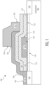
- FIG. 1 is a cross-sectional schematic view of example transistor 100 provided with a first electrically conductive_electrode (a gate electrode 1301 and a second electrically conductive electrode suitable for use as a field plate (a field plate 150) according to embodiments herein.
- the transistor 100 is formed on a semiconductor substrate 102 and has a channel region 110 near a top surface 112 of the substrate 102.
- the transistor includes a first current terminal 120 electrically coupled to a first end of the channel region 110 and a second current terminal 125 electrically coupled to a second end of the channel region 110 opposite the first current terminal 120.
- a first dielectric material 115 is disposed on the top surface 112 overlying the channel region 110.
- the first current terminal 120 and the second current terminal 125 may be formed by any suitable method. For example, they may be appropriately doped regions within the semiconductor substrate 102, or as metallic contacts deposited within recesses in the substrate 102 or on the surface of the substrate 102.
- the gate electrode 130 contacts the channel region 110 through an aperture in the first dielectric material 115.
- the gate electrode 130 may have a first portion 132 that contacts the channel region 110 within the aperture and optionally has a second portion 134 that overhangs the first dielectric material 115.
- the gate electrode 130 is depicted as having vertical sidewalls, it will be understood that the gate electrode 130 may have any suitable geometry.
- the first portion 132 of the gate electrode 130 may have sidewalls that are curved or slanted.
- the second portion 134 of the gate electrode 130 may be have sidewalls that are curved or slanted and the top of the gate electrode 130 (farthest from the channel region 110) my have any suitable geometry.
- the gate electrode 130 is disposed in between the first current terminal 120 and the second current terminal 125 along the length of the channel region 110.
- the first current terminal 120 may be operated, for example, as a source terminal of the transistor 100 and the second current terminal 125 may be operated, for example, as a drain terminal of the transistor 100.
- the gate electrode 130 is suitable for use as a gate electrode of the transistor 100 such that, when a suitable bias voltage is applied to the gate electrode 130, the channel region 110 is configured to provide an electrically conductive path between the first current terminal 120 and the second current terminal 125.
- Additional dielectric material 140 overlies the gate electrode 130 and various portions of the channel region 110.
- This additional dielectric material 140 may include a second dielectric material 142 and a third dielectric material 144 as shown in FIG. 1 .
- the transistor 100 also includes the field plate 150 with a first end 152 disposed above the channel region 110 in between the gate electrode 130 and the second current terminal 125.
- a second end 154 of the field plate 150 overlies the gate electrode 130.
- An electrically conductive interconnect 160 has a first end 162 coupled to the first current terminal 120 and a second end 164 that electrically couples the field plate 150 to the first current terminal 120.
- the field plate 150 when the first current terminal 120 is operated as a source terminal of the transistor 100, the field plate 150 is configured to operate as source-coupled field plate.
- the conductance of the channel region 110 during operation of the transistor 100 will be influenced by the electrical potential of the gate electrode 130 and the field plate 150.
- the first end 152 of the field plate 150 is capacitively coupled to the channel region 110 across the first dielectric material 115 and the second dielectric material 142.
- the interconnect 160 is separated from the gate electrode 130 and the channel region 110 by both the dielectric materials 142, 144.
- a source-coupled field plate such as the field plate 150 may be used to reduce gate-to-drain feedback capacitance ("C GD ”) in transistors such as the transistor 100 when compared to otherwise similar transistors lacking such a field plate.
- C GD gate-to-drain feedback capacitance
- the addition of a source-coupled field plate spaced apart from a gate electrode such as the gate electrode 130 will also tend to introduce additional capacitance between the gate and the source (“C GS ”) which is often an undesirable trade-off.
- C GS gate-to-drain feedback capacitance
- a single dielectric may be deposited over a substrate that has already been provided with a channel region and a gate. In this instance, both the C GD reduction provided by a source field plate and the increased C GS associated with the field plate will depend strongly on the thickness and dielectric properties of that single dielectric layer.
- the use of multiple dielectric layers configured as described may confer certain advantages Specifically, the relative dielectric constants and thicknesses of each of these materials may be chosen to achieve desired performance characteristics and to facilitate various fabrication procedures in embodiments herein, such as mixing use of oxide and nitride materials with different dielectric constants and etch selectivity. For instance, in the example of FIG. 1 , the relative thicknesses and dielectric constants of the first dielectric material 115 and the second dielectric material 142 will tend to determine the effect of the field plate 150 (operating as a source-coupled field plate) on the channel region 110 and C GD of the transistor 100 (i.e., the capacitance between the gate electrode 130 and the second current terminal 125).
- the dielectric constants and thicknesses of the third dielectric material 144 together with the second dielectric material 142 will largely determine the addition C GS penalty.
- a material with a relatively high dielectric constant may be chosen for the dielectric material 142 to maximize the influence of the field plate 150 on the channel region 110. If the dielectric material 142 was the only material separating the interconnect 160 from the gate electrode 130, the resulting additional C GS might be undesirably large.
- the C GS penalty introduced by the field plate 150 and interconnect 160 overlying the gate electrode 130 can be mitigated by the presence of the additional dielectric material 140 (shown as a composite dielectric stack that includes the dielectric materials 140,142) in at least two ways.
- the distance between the interconnect 160 and the gate electrode 130 may be increased by the additional thickness added by the dielectric material 144 disposed over the dielectric layer 142.
- the dielectric material 144 may be chosen to have a lower dielectric constant than the dielectric material 142, further reducing unwanted additional C GS .
- the transistor 100 and/or any other example transistor according to embodiments herein may be a metal-MOSFET or MISFET fabricated on a silicon substrate or any other suitable semiconductor substrate.
- the transistor 100 is a III-V compound semiconductor-based high-electron-mobility transistor ("HEMT"), otherwise known as a heterostructure field effect transistor (“HFET").
- HEMT high-electron-mobility transistor
- HFET heterostructure field effect transistor
- the effective semiconductor channel may be a 2D electron gas (“2DEG”) formed at a semiconductor heterojunction disposed with the channel region 110 according to known techniques.
- the transistor 100 may be a gallium-nitride (GaN) based HEMT.
- GaN gallium-nitride
- a 2DEG is formed at an interface between a GaN layer and an aluminum doped layer with a stochiometric composition described by the chemical formula Al x Ga 1-x N.
- the effective channel may be buried within the channel region 110 and may not extend to the top surface 112 of the substrate above the channel region 110.
- the first dielectric material 115 may be a material that provides surface passivation for the channel region 110.
- the first dielectric material 115 may be a silicon nitride passivation layer over a GaN-based heterostructure.
- a channel region such as the channel region 110 is formed by a semiconductor heterostructure
- the top surface of a semiconductor substrate e.g., the substrate 102
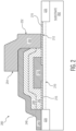
- FIG. 2 is a cross-sectional schematic view of example transistor 200 according to embodiments herein that is a variation of the example transistor 100.
- the transistor 200 is formed on a semiconductor substrate 202 (e.g., the substrate).
- the transistor 200 has a channel region 210 (e.g., the channel region 110) coupled to a first current terminal 220 and a second current terminal 225 (e.g., the current terminals 120,125) with a first electrically conductive electrode (a gate electrode 230 such as the gate electrode 130) disposed between the two current terminals.
- the gate electrode 230 (e.g., the gate electrode 130) has a first portion 232 and a second potion 234.
- the first portion 232 contacts the channel region 210 within an aperture in the dielectric material 215 (e.g., the dielectric material 115).
- the transistor 200 also includes a second electrically conductive electrode which is suitable for use a source-coupled field plate (a field plate 250, such as the field plate 150) and is electrically coupled to the first current terminal 220 via an electrically conductive interconnect 260 (e.g., the interconnect 160).
- the transistor 200 differs from the transistor 100 in that the field plate 250 is in direct contact with the first dielectric material 215 (e.g., the dielectric material 115) and without an interposing portion of the dielectric 244 (e.g., the dielectric 144).
- the transistor 200 will tend to exhibit lower C GD than the transistor 100 at the cost of a relatively small increase in C GS resulting from increased overlap of the field plate 250 with the gate electrode 230 (when the field plate 250 is operated as a source-connected field plate).
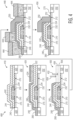
- FIGs. 3-4 illustrate example process flows for fabricating transistors with second electrodes operable as source-coupled field plates according to embodiments herein.
- FIG. 3 illustrates steps in an example process flow 300 suitable for fabricating the example transistor 100.
- FIG. 4 illustrates steps in an example process flow 400 suitable for fabricating the example transistor 200.
- the process flow 400 is substantially similar to the process flow 300. Specifically, the two processes differ
- transistors with different trade-offs between C GD and C GS may be fabricated from identical starting structures based on whether the process 300 or the process 400 is performed.
- the example process 300 includes the steps 310, 320, 330, and 350. These steps will be described with reference to the transistor 100 being fabricated during each step.
- the substrate 102 is already provided with the channel region 110, the first dielectric material 115, the first and second current terminals 120,125, and the gate electrode 130 extending within the aperture in the dielectric material 115, as described above in connection with FIG. 1 .
- the dielectric materials 142, 144 are patterned above the channel region 110 and the gate electrode 130, leaving the first current terminal 120 uncovered.
- the dielectric layers 142. 144 may be formed and patterned according to any suitable additive or subtractive method. In one example, the dielectric layers are sequentially deposited over the entire portion of the substrate 102 pictured.
- the dielectric materials 142,144 may then be covered by an etch mask material (such as photoresist) that protects the dielectric materials in areas where the dielectric materials are not to be removed.
- the dielectric material is then removed from the exposed areas using any suitable etch processes (e.g., one or more wet chemical etching and/or dry plasma etching steps).
- photoresist or other sacrificial material is patterned such that areas where the dielectric materials 142, 144 are to remain are exposed, and areas where the dielectric materials 142, 144 are not desired are protected.
- the dielectric materials are then deposited by any suitable process (e.g., RF sputtering, chemical vapor deposition, physical vapor deposition, atomic layer deposition, etc.).
- the undesired dielectric material is then removed in a lift-off process that dissolves the sacrificial material underneath the dielectric materials in areas where the dielectric materials are not desired.
- conductive material that will form the interconnect 160 once patterned.
- An additive lift-off process is pictured in which sacrificial material 322 (e.g., photoresist) has been patterned on the substrate 102.
- Conductive material is deposited by any suitable process (e.g., sputtering, thermal, electron beam evaporation, thermal evaporation, etc.) over areas covered by the sacrificial material 322 and exposed areas free of the sacrificial material 322.
- the sacrificial material 322 is dissolved, removing the conductive material 324 with it and leaving the interconnect 160 behind as shown at step 330.
- an additive lift-off process is depicted for the formation of the interconnect 160, it should be understood that well-known subtractive processes may also be suitable.
- the interconnect 160 is used as an etch mask to protect the dielectric materials 142, 144 from being removed above the gate electrode 130 and the region between the gate electrode 130 and the current terminal 120.
- the dielectric material 144 is selectively removed from the area unprotected by the interconnect 160.
- the dielectric materials 142,144 are chosen such that the dielectric material 144 is preferential removed by a chosen etching process (e.g., any suitable wet chemical etch, or dry plasma etch symbolized by the arrow 332).
- the dielectric material 142 is an oxide material (including silicon oxides and aluminum oxides as non-limiting examples) and the dielectric material 144 is a nitride material (including silicon nitrides as non-limiting examples).
- a reactive ion etching process using fluorinated compounds may be used to selectively remove only the dielectric material 144 and/or to remove the dielectric material 144 at a significantly faster rate than the dielectric material 142 (note that the area from which the dielectric 144 has been corresponds to the dashed region 334).
- the area may be "overetched" to tune the residual thickness of the dielectric material 142 that remains.
- the etch process chosen to remove the dielectric material 144 may be prolonged past the point where all the dielectric material 144 has been removed and the remaining thickness of the dielectric material 142 may be controlled by varying how long the etch time is extended beyond the time required to remove the dielectric material 144).
- the thickness of the dielectric material 142 under the field plate 150 is one factor that determines the C GD reduction (compared to a device with no source field plate) enabled by the field plate 150.
- the dielectric material 142 is a nitride material (inducing silicon nitrides as non-limiting examples) and the dielectric material 144 is an oxide material (including silicon oxides and aluminum oxides as non-limiting examples).
- conductive material that will form the field plate 150 is patterned.
- An additive lift-off process is pictured in which sacrificial material 342 (e.g., photoresist) has been patterned on the substrate 102.
- Conductive material is deposited by any suitable process (e.g., sputtering, thermal, electron beam evaporation, thermal evaporation, etc.) over areas covered by the sacrificial material 342 and exposed areas free of the sacrificial material 342.
- the sacrificial material 322 may be dissolved, removing the conductive material 344 with it and leaving the field plate 150 behind as shown at step 340.
- an additive lift-off process is depicted for the formation of the field plate 150, it should be understood that well-known subtractive processes may also be suitable.
- the dielectric material 142 remaining above the current terminal 125 is optionally removed to allow for the addition of a conductive via in electrical contact with the current terminal 125.
- the example process 400 includes the steps 410, 420, 430, and 450. These steps will be described with reference to the transistor 100 being fabricated during each step.
- the substrate 202 is already provided with the channel region 210, the first dielectric material 215, the first and second current terminals 220, 225, and the gate electrode 230 extending within the aperture in the dielectric material 215, as described above in connection with FIG. 2 .
- the dielectric materials 242,244 are patterned above the channel region 210 and the gate electrode 230, leaving the first current terminal 220 uncovered.
- the dielectric materials 242,244 may be formed and patterned according to any suitable additive or subtractive method, as described above in connection with step 310 of the process 300.
- conductive material that will form the interconnect 260 once patterned is deposited, as described above in connection with step 320 of the process 300.
- An additive lift-off process is pictured in which sacrificial material 422 (e.g., sacrificial material 322) has been patterned on the substrate 202 as described in connection with step 320 of the process 300.
- the sacrificial material 422 is removed, removing the conductive material 424 (e.g., the conductive material 324) with it and leaving the interconnect 260 behind as shown at step 430.
- an additive lift-off process is depicted for the formation of the interconnect 260, it should be understood that well-known subtractive processes may also be suitable.
- the interconnect 260 is used as an etch mask to protect the dielectric materials 242, 244 from being removed above the electrode 230 and the region between the electrode 230 and the current terminal 220.
- the dielectric material 244 is selectively removed from the area unprotected by the interconnect 260 as described above in connection with step 330 of the process 300.
- step 430 includes removing both layers of the dielectric material 244,242 (e.g., the dielectric materials 144, 142).
- the dashed regions 438, 436 indicate the areas from which the dielectric material has been removed
- the dielectric materials 242,244 are chosen such that the dielectric material 244 is preferentially removed by a chosen etching process (e.g., any suitable wet chemical etch, or dry plasma etch) such that etching of the dielectric material 242 proceeds more slowly than etching of the dielectric material 244.
- a chosen etching process e.g., any suitable wet chemical etch, or dry plasma etch
- two distinctive etch processes are used: a first etch process 432 (symbolized by a vertical arrow) that removes the dielectric material 244 and a subsequent optional etch process 434 removes the dielectric material 242.
- the subsequent etch used to remove the dielectric material 242 is a wet etch process.
- the dielectric material 215 e.g., the dielectric material 115
- the dielectric material 215 is a thin material (e.g., silicon nitride having a thickness less than 1000 ⁇ ngstr ö ms) that passivates the top surface 212 above the channel region 210
- wet etching may be desirable to avoid etch-induced damage to the dielectric material 215 which might adversely affect performance of the transistor 200 (e.g., by introducing charge-trapping states in the semiconductor band structure of the channel region 210).
- conductive material that will form the field plate 250 is patterned similarly to the description of step 340 of process 300.
- An additive lift-off process is pictured in which sacrificial material 442 (e.g., the sacrificial material 342) has been patterned on the substrate 202.
- Conductive material is deposited by any suitable process (e.g., sputtering, thermal, electron beam evaporation, thermal evaporation, etc.) over areas covered by the sacrificial material 442 and exposed areas free of the sacrificial material 442.
- the sacrificial material 442 may be dissolved, removing the conductive material 444 with it and leaving the field plate 250behind as shown at step 450.
- an additive lift-off process is depicted for the formation of the field plate 250, it should be understood that well-known subtractive processes may also be suitable.
- step 450 after the sacrificial material 442, and with it, the undesired conductive material 444 is removed, the dielectric material 244 remaining above the current terminal 225 is optionally removed to allow for the addition of a conductive via in electrical contact with the current terminal 225.
- respective interconnects e.g., interconnects 160,260
- etch mask that at least partially defines the location of subsequently formed field plates 150,250 configured for operation as source-connected field plates that are disposed, in part, above the interconnects 160,260.
- electrodes similar to the field plates 150,250 are disposed (at least partially below) interconnects similar to the interconnects 160, 260.
- FIG. 5 is a cross-sectional schematic view of example transistor 500 according to embodiments herein that may be understood as a variation of the example transistor 100.
- the transistor 500 is formed on a semiconductor substrate 502 (e.g., the substrate 102).
- the transistor 500 has a channel region 510 (e.g., a channel region 110,210) coupled to a first current terminal 520 and a second current terminal 525 (e.g., current terminals 120,125 or 220,225) with a gate electrode 530 (e.g., a gate electrode 130,230) disposed between the two terminals.
- a channel region 510 e.g., a channel region 110,210
- a second current terminal 525 e.g., current terminals 120,125 or 220,225
- a gate electrode 530 e.g., a gate electrode 130,230
- the gate electrode 530 has a first portion 532 and a second potion 534 (e.g., a first portion 132,232 and/or a second portion 134,234 of a respective gate electrode 130,230).
- the first portion 532 contacts the channel region 510 within an aperture in the dielectric material 515 (e.g., dielectric material 115,215).
- the transistor 500 also includes a second electrode which is suitable for use a source-coupled field plate (a field plate 550; e.g., a field plate 150,250) and is electrically coupled to the first current terminal 520 via an electrically conductive interconnect 560 (e.g., an interconnect 160,260).
- the field plate 550 may extend all the way to the current terminal 520 in or more areas (e.g., in the cross-sectional plane depicted or in a different cross-sectional plane) and the separate interconnect 560 may be absent.
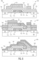
- the example process 600 includes the steps 610, 620, 630, 640, and 650. These steps will be described with reference to the transistor 500 being fabricated during each step.
- the substrate 502 is already provided with the channel region 510, the first dielectric material 515, the first and second current terminals 520, 525, and the gate electrode 530 extending within the aperture in the dielectric material 515, as described above in connection with FIG. 1 .
- etch masking material 612 is patterned above the dielectric materials 544, 542 and etch process 614 (signified by vertical arrows) configured to selectively remove the dialectic material 544 is performed.
- the etch masking material 612 may be any suitable material configured to withstand the etch process 614 configured to selectively remove the dialectic material 544.
- the etch masking material 612 may be patterned using any suitable additive or subtractive process including examples described herein and/or other well-known techniques.
- the dielectric layer 544 is patterned above the channel region 510, the current terminals 520, 525 and the gate electrode 530, thereby exposing the dielectric material 542 above the current terminals 520,525 creating an aperture in the dielectric material 544 for the field plate 550, as visible at step 620 in FIG. 6 .
- the process 600 may be altered such that the field plate 550 extends all the way to the current terminal 520 in or more areas (e.g., in the cross-sectional plane depicted or in a different cross-sectional plane) and the separate interconnect 560 may be absent.
- the etch process 614 is chosen, at least in part, for compatibility with other materials (i.e., the dielectric material 542 and the masking material 612).
- the dielectric material 542 is an oxide material such as silicon oxide (SiOz or SiO x where x is a fractional value that is less than or greater than two) or aluminum oxide (Al 2 O 3 or Al 2 O x where x is a value other than three)
- the dielectric material 544 is a nitride material such as silicon nitride (Si 3 N 4 or Si 3 N x where x is value other than four)
- the masking material 612 is photoresist.
- the etch process 614 may be a wet chemical etch that preferentially removes the dielectric material 544 over the dielectric material 542 and the etch mask material 612 such as a wet etching process that uses a buffered oxide etchant (BOE) solution.
- a dry plasma etching process such as a fluorine-based reactive ion etching process (using SF 4 , as one non-limiting example) may be used.
- step 620 conductive material that will form the field plate 550 once patterned is deposited
- sacrificial material 622 e.g., sacrificial material 322 or other suitable material has been patterned on the substrate 502.
- the sacrificial material 612 is removed, removing the conductive material 624 with it, leaving the field plate 550 behind as shown at step 630.
- an additive lift-off process is depicted for the formation of the field plate 550, it should be understood that well-known subtractive processes may also be suitable in which a layer is deposited and patterned by etching material that is not protected by an etch mask is removed by a suitable wet chemical or dry plasma etching process.
- step 620 is altered the field plate 550 extends all the way to the current terminal 520 in or more areas (e.g., in the cross-sectional plane depicted or in a different cross-sectional plane).
- an etch process 634 (signified by arrows) is performed.
- the etch process 634 is configured to selectively remove the dielectric material 542 that is not protected by the dielectric material 544, as patterned at step 610. Any suitable etch process may be used, including wet chemical etches and dry plasma etches. It will be understood that the choice of etching process for the etch process 634 may depend on choices for various other materials (e.g., the dielectric materials 515, 544 and the conductive material used for the field plate 550).
- the dielectric material 542 may be an oxide material (non-limiting examples of which include an aluminum oxide material or a silicon oxide material) and the dielectric material 544 may be a nitride material (e.g., a silicon nitride material).
- a reactive ion etching process using fluorinated gases may be used to preferentially remove the nitride materials while leaving oxide materials intact.
- conductive material that will form the interconnect 560 once patterned is deposited, as described above in connection with steps 320, 420 of the processes 300,400 respectively.
- An additive lift-off process is pictured in which sacrificial material 642 (e.g., sacrificial material 322) has been patterned on the substrate 502 as described in connection with step 320 of the process 300.
- the sacrificial material 642 is removed, removing the conductive material 644 (e.g., the conductive material 324) with it, leaving the interconnect 760.
- step 640 may not be required.
- FIG. 7 is a cross-sectional schematic view of example transistor 700 according to embodiments herein that may be understood as a variation of the example transistor 500 in which the source-connected field plate (the field plate 750) directly contacts the dielectric material 715 (e.g., dielectric material 115, 215, 515) rather than an intervening dielectric layer (e.g., the dielectric material 544) as seen in the transistor 500 as depicted in FIG. 5 .
- the source-connected field plate the field plate 750
- the dielectric material 715 e.g., dielectric material 115, 215, 515
- an intervening dielectric layer e.g., the dielectric material 544
- the transistor 700 is formed on a semiconductor substrate 702 (e.g., a substrate 102,202,502).
- the transistor 700 has a channel region 710 (e.g., a channel region 110, 210, 510 coupled to a first current terminal 720 and a second current terminal 725 (e.g., current terminals 120,125, 220,225, and/or 520,525) with a gate electrode 730 (e.g., an electrode 130,230,530) disposed between the two terminals.
- the gate electrode 730 has a first portion 732 and a second portion 734 (e.g., a first portion 132,232,532 and/or a second portion 134,234,534 of a respective electrode 130,230,530).
- the first portion 732 contacts the channel region 710 within an aperture in the dielectric material 715 (e.g., dielectric material 115,215,515).
- the transistor 700 also includes the second electrode which is suitable for use a source-coupled field plate (a field plate 750; e.g., a field plate 150,250,550) and is electrically coupled to the first current terminal 720 via an electrically conductive interconnect 760 (e.g., an interconnect 160,260,560).
- the field plate 750 may extend all the way to the current terminal 720 in or more areas (e.g., in the cross-sectional plane depicted or in a different cross-sectional plane)and the separate interconnect 760 is absent.
- the example process 800 includes the steps 810, 820, 830, and 840. These steps will be described with reference to the transistor 700 being fabricated during each step.
- the substrate 702 is already provided with the channel region 710, the first dielectric material 715, the first and second current terminals 720,725 and the gate electrode 730 extending within the aperture in the dielectric material 715, as described above in connection with FIG. 7 . It will be apparent that the process 800 has the advantage of requiring few processing steps than the process 600 as will be explained further below.
- the process 800 may be altered such that the field plate 750 extends all the way to the current terminal 720 in or more areas (e.g., in the cross-sectional plane depicted or in a different cross-sectional plane)and the separate interconnect 760 may be absent.
- etch masking material 812 is patterned above the dielectric materials 744, 742 and an etch process 814 (signified by vertical arrows) configured to selectively remove the both the dielectric material 744 and the dielectric material 742 is performed.
- the etch masking material 812 may be any suitable material configured to withstand the etch process 814.
- the etch masking material 812 may be patterned using any suitable additive or subtractive process including examples described herein and/or other well-known techniques. It will be understood that the etch process 814 will be chosen, at least in part, for compatibility with other materials (i.e., the dielectric material 715 and the etch masking material 812). For instance, the etch process 814 should not cause excessive damage to the dielectric material 715 directly overlying the channel region 710.
- the dielectric material 742 is an oxide material (including aluminum oxides and silicon oxides as non-limiting examples)
- the dielectric material 744 is a nitride material (including silicon nitrides as non-limiting examples)
- the etch masking material 812 is any suitable photoresist.
- the etch process 814 may be a wet chemical etch that preferentially removes the dielectric material 744 over the dielectric material 742 and the etch mask material (including a wet etch using buffered oxide etchant (BOE) solution, as a non-limiting example).
- BOE buffered oxide etchant
- a dry plasma etching process including fluorine-based reactive ion etching processes as non-limiting examples may be used.
- the process 800 (particularly the step 810) enables the dielectric materials 744, 742 to be removed above both the current terminals 720, 725 at the same time that the opening for the first end 752 of the field plate 750 is made.
- the process 800 does not require a step similar to step 640 of the process 600 (in which dielectric material 742 remaining above the current terminal 520 and/or the current terminal 525 must be removed).
- step 820 e.g., step 620 of the process 600
- conductive material that will form the field plate 750 once patterned is deposited.
- An additive lift-off process is pictured in which sacrificial material 822 (e.g., sacrificial material 322, 622 or other suitable material) has been patterned on the substrate 702. The sacrificial material 822 is removed, removing the unwanted conductive material 824 with and leaving the field plate 750 behind as shown at step 830.
- step 820 is altered such that the field plate 750 extends all the way to the current terminal 720in or more areas (e.g., in the cross-sectional plane depicted or in a different cross-sectional plane).
- the sacrificial material 822 is also absent above the current terminal 725 step 820.
- step 830 may be omitted.
- conductive material that will form the interconnect 760 once patterned is deposited, as described above in connection with steps 320, 420 of the processes 300,400 respectively.
- An additive lift-off process is pictured in which sacrificial material 832 (e.g., sacrificial material 322, 642) has been patterned on the substrate 702 as described in connection with step 840 of the process 800.
- the sacrificial material 832 is removed, removing the conductive material 834 (e.g., conductive material 324, 644) with it, leaving the interconnect 760.
- FIG. 9A is a cross-sectional schematic view of example transistor 900 according to embodiments herein in which the electrode operable as a source-connected field plate 950; (e.g., a field plate 250, 550, or 750) configured to be operable as a source-connected field plate) is provided with an extension 956 in between a first end 952 and a second end 954 of the field plate 950 that is disposed between the current terminal 925 and the first end 952 of the field plate 950 that is disposed above the channel region 910 and separated from the channel region 910 by the dielectric material 915.
- a source-connected field plate 950 e.g., a field plate 250, 550, or 750
- extension 956 of the field plate 950 will tend to lower electric fields arising in the vicinity of the dashed region 957 due to the presence of the corner of the field plate 950 nearest the second current terminal 925 (operable as the drain of the transistor 900).
- FIG. 9B shows a portion of the transistor 900 during a processing step 920 that is similar to the step 820 of the process 800.
- the difference in step 920 is that the sacrificial material 922 is patterned such that the extension 956 is disposed above the dielectric materials 944, 942.
- the steps of various processes above are non-limiting examples of suitable processes according to embodiments herein and are for the purposes of illustration.
- Devices according to embodiments herein may be fabricated using any suitable processes including those that omit steps described above, perform those steps and similar steps in different orders, and the like.
- the transistor 500 may be fabricated in a process that exposes the current terminal 520 and 525 in different steps (instead of a single step as shown in step 630).
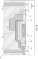
- FIG 10 shows a cross-sectional schematic view of a transistor 1000 in which additional dielectric material encapsulates the active structures and provides isolation between vias.
- the transistor 1000 has an isolation dielectric 1080 in which a source via 1021 is disposed that electrically contacts the first current terminal 1020 via the interconnect 1060 and a drain via 1026 that electrically contacts the second current terminal 1025.
- a gate via electrically contacting the gate electrode 1030 may be present but would not be visible in the cross-sectional plane depicted in FIG. 10 .
- Example 1 A method of fabricating a semiconductor device that includes depositing interlayer dielectric material over a first dielectric layer and a first electrode on a semiconductor substrate.
- the first dielectric layer is disposed above a channel region of the semiconductor substrate suitable for use as a semiconductive transistor channel; the first electrode extends within a first aperture in the first dielectric layer and contacts a top surface of the channel region within the aperture; and the first electrode is disposed between a first current terminal electrically coupled to a first end of the channel region and a second current terminal electrically coupled to a second end the channel region opposite the first end of the channel region.
- the method further includes performing a first patterning step that includes selectively removing the interlayer dielectric material in a first region between the first electrode and the second current terminal, thereby leaving remaining dielectric material that includes the first dielectric material above the channel region.
- the method also includes forming a second electrode in the first region having first and second ends. The first end of the second electrode is adjacent to the first electrode. The first end of the second electrode separated from the top surface of the channel region by at least the first dielectric layer. The second end of the second electrode is disposed above the first electrode and is separated from the first electrode by the remaining interlayer dielectric material.
- the method further includes forming a conductive interconnect that extends between the first current terminal and the second electrode and electrically couples the second electrode to the first current terminal.
- the interconnect is disposed above the first electrode and the remaining interlayer dielectric material.
- Example 2 A method as in Example 1, in which the interlayer dielectric material includes a first interlayer dielectric material and a second interlayer dielectric material layer disposed above the first interlayer dielectric material.
- selectively removing the interlayer dielectric material in the first region further includes forming a second aperture in the second dielectric layer by removing the second interlayer dielectric from the first region.
- the first end of the second electrode extends within the second aperture; and the first end of the second electrode is separated from the channel region in the second aperture by the first dielectric material and a portion of the first interlayer dielectric material disposed beneath the second aperture.
- Example 3 A method as in Example 2, in which forming the second aperture in the second dielectric layer includes performing an etching procedure that preferentially etches the second interlayer dielectric material over the first interlayer dielectric material for an amount of time chosen to leave a desired thickness of the first interlayer dielectric material intact in the first region.
- Example 4 A method as in either of Examples 2 or 3, in which forming the second electrode in the first region includes depositing conductive material that fills the second aperture and also forms an extension area adjacent to the second aperture wherein the conductive material overlies the interlayer dielectric material.
- Example 5 A method as in any of Examples 1-4, in which wherein the interlayer dielectric material comprises a first interlayer dielectric material and a second interlayer dielectric material layer disposed above the first interlayer dielectric material.
- selectively removing the interlayer dielectric material in the first region further includes forming a second aperture in the second interlayer dielectric material by removing the second interlayer dielectric material from the first region using a first etching procedure followed by removing the first interlayer dielectric material from the first region using a second etching procedure.
- the first end of the second electrode extends within the second aperture.
- Example 6 A method as in any of Examples 2-5 in which forming the second electrode in the first region comprises depositing conductive material that fills the second aperture and also forms an extension area adjacent to the second aperture wherein the conductive material overlies the interlayer dielectric material.
- Example 7 A method as in any of Examples 5-6, in which the first etching procedure is a dry plasma etching procedure and the second etching procedure is a wet chemical etching procedure.
- Example 8 A method as in any of Examples 5-7 that further includes forming a first via opening that exposes the first current terminal by removing the second interlayer dielectric material from a region above the first current terminal using the first etching procedure followed by removing the first interlayer dielectric material from the region above the first current terminal using the second etching procedure.
- This Example also includes forming a second via opening that exposes the second current terminal by removing the second interlayer dielectric material from a region above the second current terminal using the first etching procedure followed by removing the first interlayer dielectric material from the region above the second current terminal using the second etching procedure.
- Example 9 A method as in Example 7, in which forming the interconnect includes depositing conductive material that fills the first via opening.
- Example 10 A method as in any of Examples 1-9, in which selectively removing the interlayer dielectric material in the first region includes performing an etching procedure that preferentially etches the interlayer dielectric material over the first dielectric material for an amount of time chosen to leave the first dielectric material intact in the first region.
- Example 11 A method as in any of Examples 1-10, in which forming the second electrode in the first region comprises depositing conductive material that fills the second aperture and also forms an extension area adjacent to the second aperture wherein the conductive material overlies the first interlayer dielectric material.
- Example 12 A method as in any of Examples 1-11, in which performing the etching procedure that preferentially etches the interlayer dielectric material over the first dielectric material also includes: forming a first via opening that exposes the first current terminal by removing the interlayer dielectric material from a region above the first current terminal; and forming a second via opening that exposes the second current terminal by removing the interlayer dielectric material from a region above the first current terminal.
- the interconnect is formed before the second electrode is formed; a first end of the interconnect electrically contacts the first terminal within the first via opening; and a second end of the interconnect electrically contacts the second end of the second electrode.
- Example 13 A semiconductor device that includes: a channel region defined in a semiconductor substrate; a first current terminal electrically coupled to a first end of the channel region; and a second current terminal electrically coupled to a second end of the channel region opposite the first end.
- the device also has a first dielectric material having a first dielectric thickness and overlying the channel region; a first interlayer dielectric material overlying the channel and the first electrode; and second interlayer dielectric material overlying the first interlayer dielectric material.
- the device has a first aperture in the first dielectric material that overlies the channel region in between the first current terminal and the second current terminal; and an electrically conductive first electrode that extends within the first aperture that is in direct physical contact with a top surface of the channel region.
- the device also has an electrically conductive second electrode spaced apart from the first electrode.
- the second electrode has a first end that overlies at least the first dielectric material and the channel region at a location between the first electrode and the second current terminal; and a second end that overlies at least a portion of the first electrode that is separated from the first electrode by the first and second interlayer dielectric materials.
- the device is configured to provide an electrically conductive path from the first current terminal to the second current terminal via the channel region when a sufficient control voltage is applied to the first electrode.
- Example 14 A device as in Example 13, in which the first end of the second electrode directly contacts the first dielectric layer; and the second electrode further includes an electrode extension that is disposed between the first end of the second and the second current terminal and is disposed above at least the first interlayer dielectric material.
- Example 15 A device as in either of Examples 13 or 14, in which the first end of the second electrode directly contacts the first dielectric material; the first interlayer dielectric material and the second interlayer dielectric material have been removed from an area above the first dielectric material and beneath the first end of the second electrode; the first interlayer dielectric material has been removed by an etching procedure and is characterized by a first etch rate with respect to the etching procedure; and the first dielectric material is characterized by a second etch rate with respect to the etching procedure that is slower than the first etch rate.
- Example 16 A device as in any of Examples 13-15, that further includes an electrically conductive interconnect that electrically couples the second electrode to the first current terminal, the interconnect overlying the first electrode and the first and second interlayer dielectric materials, and separated from the first electrode by the first and second interlayer dielectric materials.
- Example 17 A device as in Example 16 in which wherein the interconnect electrically contacts the second electrode at the second end of the second electrode at a location overlying the first electrode
- Example 18 A device as in any of Examples 13-17, in which the second electrode includes a lateral extension that overlies the second interlayer dielectric material at a location between the first end of the second electrode and the second current terminal.
- Example 19 A device as in any of Examples 13-18, in which the first end of the second electrode directly overlies the first interlayer dielectric material; and the second interlayer dielectric material is absent from an area above the first interlayer dielectric material and beneath the first end of the second electrode.
- the first interlayer dielectric material is characterized by a first etch rate with respect to a dry etching procedure; and the second interlayer dielectric material is characterized by a second etch rate with respect to the dry etching procedure that is faster than the first etch rate.
- Example 20 A device as in any of Examples 13-19, in which the channel region comprises a semiconductor heterostructure with a two-dimensional electron gas (2DEG) region formed at a semiconductor heterojunction beneath a surface of the channel region nearest to the first electrode.
- 2DEG two-dimensional electron gas
- Placement of a field plate in a field-effect transistor is optimized by using multiple dielectric layers such that a first end of field plate is separated from a channel region of the transistor by a first set of one or more distinct dielectric material layers. A second end of the field plate overlies the channel region and a gate electrode from which it is separated by the first set of dielectric layers and one or more additional dielectric layers.
- node or “terminal” means any internal or external reference point, connection point, junction, signal line, conductive element, or the like, at which a given signal, logic level, voltage, data pattern, current, or quantity is present.
- two or more nodes may be realized by one physical element (and two or more signals can be multiplexed, modulated, or otherwise distinguished even though received or output at a common node).
Landscapes
- Insulated Gate Type Field-Effect Transistor (AREA)
- Junction Field-Effect Transistors (AREA)
- Thin Film Transistor (AREA)
Applications Claiming Priority (1)
| Application Number | Priority Date | Filing Date | Title |
|---|---|---|---|
| US17/645,276 US12342560B2 (en) | 2021-12-20 | 2021-12-20 | Transistors with source-connected field plates |
Publications (2)
| Publication Number | Publication Date |
|---|---|
| EP4199104A2 true EP4199104A2 (de) | 2023-06-21 |
| EP4199104A3 EP4199104A3 (de) | 2023-10-18 |
Family
ID=84829953
Family Applications (1)
| Application Number | Title | Priority Date | Filing Date |
|---|---|---|---|
| EP22214206.9A Withdrawn EP4199104A3 (de) | 2021-12-20 | 2022-12-16 | Transistoren mit source-verbundenen feldplatten |
Country Status (3)
| Country | Link |
|---|---|
| US (2) | US12342560B2 (de) |
| EP (1) | EP4199104A3 (de) |
| CN (1) | CN116313791A (de) |
Family Cites Families (30)
| Publication number | Priority date | Publication date | Assignee | Title |
|---|---|---|---|---|
| US7501669B2 (en) | 2003-09-09 | 2009-03-10 | Cree, Inc. | Wide bandgap transistor devices with field plates |
| CA2538077C (en) | 2003-09-09 | 2015-09-01 | The Regents Of The University Of California | Fabrication of single or multiple gate field plates |
| US6867078B1 (en) | 2003-11-19 | 2005-03-15 | Freescale Semiconductor, Inc. | Method for forming a microwave field effect transistor with high operating voltage |
| JP2006086398A (ja) * | 2004-09-17 | 2006-03-30 | Matsushita Electric Ind Co Ltd | 半導体装置及びその製造方法 |
| US7592211B2 (en) | 2006-01-17 | 2009-09-22 | Cree, Inc. | Methods of fabricating transistors including supported gate electrodes |
| US7709269B2 (en) | 2006-01-17 | 2010-05-04 | Cree, Inc. | Methods of fabricating transistors including dielectrically-supported gate electrodes |
| KR100782430B1 (ko) | 2006-09-22 | 2007-12-05 | 한국과학기술원 | 고전력을 위한 내부전계전극을 갖는 갈륨나이트라이드기반의 고전자 이동도 트랜지스터 구조 |
| US8283699B2 (en) | 2006-11-13 | 2012-10-09 | Cree, Inc. | GaN based HEMTs with buried field plates |
| KR101583094B1 (ko) | 2010-12-14 | 2016-01-07 | 한국전자통신연구원 | 반도체 소자 및 이의 제조방법 |
| JP2013157407A (ja) | 2012-01-27 | 2013-08-15 | Fujitsu Semiconductor Ltd | 化合物半導体装置及びその製造方法 |
| US9111868B2 (en) | 2012-06-26 | 2015-08-18 | Freescale Semiconductor, Inc. | Semiconductor device with selectively etched surface passivation |
| US9024324B2 (en) | 2012-09-05 | 2015-05-05 | Freescale Semiconductor, Inc. | GaN dual field plate device with single field plate metal |
| US8946779B2 (en) | 2013-02-26 | 2015-02-03 | Freescale Semiconductor, Inc. | MISHFET and Schottky device integration |
| US9142626B1 (en) | 2013-04-23 | 2015-09-22 | Hrl Laboratories, Llc | Stepped field plate wide bandgap field-effect transistor and method |
| US9847411B2 (en) | 2013-06-09 | 2017-12-19 | Cree, Inc. | Recessed field plate transistor structures |
| US9755059B2 (en) | 2013-06-09 | 2017-09-05 | Cree, Inc. | Cascode structures with GaN cap layers |
| JP2015195288A (ja) * | 2014-03-31 | 2015-11-05 | 住友電工デバイス・イノベーション株式会社 | 半導体装置及び半導体装置の製造方法 |
| US9911817B2 (en) | 2015-07-17 | 2018-03-06 | Cambridge Electronics, Inc. | Field-plate structures for semiconductor devices |
| WO2017069464A1 (ko) * | 2015-10-22 | 2017-04-27 | (주)기가레인 | 고전자이동도 트랜지스터 및 그의 제조방법 |
| EP3174102B1 (de) | 2015-11-27 | 2022-09-28 | Nexperia B.V. | Halbleiterbauelement und verfahren zur herstellung eines halbleiterbauelements |
| US9741840B1 (en) | 2016-06-14 | 2017-08-22 | Semiconductor Components Industries, Llc | Electronic device including a multiple channel HEMT and an insulated gate electrode |
| US10497602B2 (en) | 2016-08-01 | 2019-12-03 | Semiconductor Components Industries, Llc | Process of forming an electronic device including forming an electronic component and removing a portion of a substrate |
| US20190028066A1 (en) * | 2017-07-24 | 2019-01-24 | Macom Technology Solutions Holdings, Inc. | Fet operational temperature determination by field plate resistance thermometry |
| US20190097001A1 (en) | 2017-09-25 | 2019-03-28 | Raytheon Company | Electrode structure for field effect transistor |
| US10700188B2 (en) | 2017-11-02 | 2020-06-30 | Rohm Co., Ltd. | Group III nitride semiconductor device with first and second conductive layers |
| EP3905335A1 (de) | 2020-04-28 | 2021-11-03 | Infineon Technologies AG | Gruppe-iii-nitrid-basierte transistorvorrichtung |
| US11355636B2 (en) | 2020-05-29 | 2022-06-07 | metaMOS Solutions Inc. | Radio frequency (RF) switch device on silicon-on-insulator (SOI) and method for fabricating thereof |
| CN112326610A (zh) | 2020-10-28 | 2021-02-05 | 瑞莱生物科技江苏有限公司 | 一种定量荧光检测光学装置 |
| CN113628964B (zh) | 2021-08-04 | 2024-03-12 | 苏州英嘉通半导体有限公司 | Ⅲ族氮化物增强型hemt器件及其制造方法 |
| US12148820B2 (en) * | 2021-12-20 | 2024-11-19 | Nxp B.V. | Transistors with source-connected field plates |
-
2021
- 2021-12-20 US US17/645,276 patent/US12342560B2/en active Active
-
2022
- 2022-11-14 CN CN202211417068.0A patent/CN116313791A/zh active Pending
- 2022-12-16 EP EP22214206.9A patent/EP4199104A3/de not_active Withdrawn
-
2025
- 2025-05-05 US US19/198,640 patent/US20250267885A1/en active Pending
Also Published As
| Publication number | Publication date |
|---|---|
| EP4199104A3 (de) | 2023-10-18 |
| US20230197829A1 (en) | 2023-06-22 |
| US20250267885A1 (en) | 2025-08-21 |
| CN116313791A (zh) | 2023-06-23 |
| US12342560B2 (en) | 2025-06-24 |
Similar Documents
| Publication | Publication Date | Title |
|---|---|---|
| US12148820B2 (en) | Transistors with source-connected field plates | |
| KR102339311B1 (ko) | 반도체 소자 및 그 제조 방법 | |
| CN106684140B (zh) | 半导体器件及其制造方法 | |
| US20160343809A1 (en) | Device with a conductive feature formed over a cavity and method therefor | |
| KR101689137B1 (ko) | 모놀리식 집적 회로(mmic) 구조 및 이러한 구조를 형성하기 위한 방법 | |
| EP3948955B1 (de) | T-gate mt miniaturfeldplatte und herstellungsverfahren dafür | |
| US11538908B2 (en) | Semiconductor device | |
| KR20150083483A (ko) | 고전압 구동용 전계효과 트랜지스터 및 제조 방법 | |
| EP4199105A1 (de) | Transistoren mit source-verbundenen feldplatten | |
| JP5162823B2 (ja) | 半導体装置及び半導体装置の製造方法 | |
| US12369380B2 (en) | Transistor with dielectric spacers and field plate and method of fabrication therefor | |
| EP4199104A2 (de) | Transistoren mit source-verbundenen feldplatten | |
| US20230207675A1 (en) | Semiconductor device with a gate electrode having multiple regions and method of fabrication therefor | |
| US12165871B2 (en) | Method for manufacturing a gate terminal of a HEMT device, and HEMT device | |
| TWI521641B (zh) | 製作氮化鎵裝置及積體電路中之自我對準隔離部的方法 | |
| CN113964103A (zh) | 半导体器件及其制备方法 | |
| US12266713B2 (en) | Transistor with dielectric spacers and method of fabrication therefor | |
| CN116779457A (zh) | 嵌入半导体晶片中的密封腔 | |
| US12349433B2 (en) | Transistors with self-aligned source-connected field plates | |
| US20250210409A1 (en) | Device with electrical component formed over a cavity and method therefor | |
| EP4590085A1 (de) | Verbesserte verarmungstyp-hemt-vorrichtung und herstellungsverfahren dafür | |
| CN111987155A (zh) | 高电子迁移率晶体管装置及其制造方法 | |
| TW202404087A (zh) | 高電子遷移率電晶體元件的製造方法 | |
| CN119922936A (zh) | 具有多阶梯栅极和多阶梯场板的半导体装置和其制造方法 | |
| CN119947199A (zh) | 具有多阶梯栅极及多阶梯场板的半导体装置及其制造方法 |
Legal Events
| Date | Code | Title | Description |
|---|---|---|---|
| PUAI | Public reference made under article 153(3) epc to a published international application that has entered the european phase |
Free format text: ORIGINAL CODE: 0009012 |
|
| STAA | Information on the status of an ep patent application or granted ep patent |
Free format text: STATUS: THE APPLICATION HAS BEEN PUBLISHED |
|
| AK | Designated contracting states |
Kind code of ref document: A2 Designated state(s): AL AT BE BG CH CY CZ DE DK EE ES FI FR GB GR HR HU IE IS IT LI LT LU LV MC ME MK MT NL NO PL PT RO RS SE SI SK SM TR |
|
| PUAL | Search report despatched |
Free format text: ORIGINAL CODE: 0009013 |
|
| AK | Designated contracting states |
Kind code of ref document: A3 Designated state(s): AL AT BE BG CH CY CZ DE DK EE ES FI FR GB GR HR HU IE IS IT LI LT LU LV MC ME MK MT NL NO PL PT RO RS SE SI SK SM TR |
|
| RIC1 | Information provided on ipc code assigned before grant |
Ipc: H01L 29/20 20060101ALN20230911BHEP Ipc: H01L 21/338 20060101ALN20230911BHEP Ipc: H01L 29/778 20060101ALN20230911BHEP Ipc: H01L 29/41 20060101AFI20230911BHEP |
|
| STAA | Information on the status of an ep patent application or granted ep patent |
Free format text: STATUS: THE APPLICATION IS DEEMED TO BE WITHDRAWN |
|
| 18D | Application deemed to be withdrawn |
Effective date: 20240419 |