EP4191663A1 - Verfahren zur herstellung einer sic-basierten elektronischen vorrichtung mit einer passivierungsschicht und einem verankerungselement und einer dadurch hergestellten elektronischen vorrichtung - Google Patents
Verfahren zur herstellung einer sic-basierten elektronischen vorrichtung mit einer passivierungsschicht und einem verankerungselement und einer dadurch hergestellten elektronischen vorrichtung Download PDFInfo
- Publication number
- EP4191663A1 EP4191663A1 EP22207266.2A EP22207266A EP4191663A1 EP 4191663 A1 EP4191663 A1 EP 4191663A1 EP 22207266 A EP22207266 A EP 22207266A EP 4191663 A1 EP4191663 A1 EP 4191663A1
- Authority
- EP
- European Patent Office
- Prior art keywords
- layer
- insulating layer
- insulating
- anchoring element
- electronic device
- Prior art date
- Legal status (The legal status is an assumption and is not a legal conclusion. Google has not performed a legal analysis and makes no representation as to the accuracy of the status listed.)
- Granted
Links
Images


Classifications
-
- H—ELECTRICITY
- H10—SEMICONDUCTOR DEVICES; ELECTRIC SOLID-STATE DEVICES NOT OTHERWISE PROVIDED FOR
- H10W—GENERIC PACKAGES, INTERCONNECTIONS, CONNECTORS OR OTHER CONSTRUCTIONAL DETAILS OF DEVICES COVERED BY CLASS H10
- H10W74/00—Encapsulations, e.g. protective coatings
- H10W74/10—Encapsulations, e.g. protective coatings characterised by their shape or disposition
- H10W74/111—Encapsulations, e.g. protective coatings characterised by their shape or disposition the semiconductor body being completely enclosed
- H10W74/127—Encapsulations, e.g. protective coatings characterised by their shape or disposition the semiconductor body being completely enclosed characterised by arrangements for sealing or adhesion
-
- H—ELECTRICITY
- H10—SEMICONDUCTOR DEVICES; ELECTRIC SOLID-STATE DEVICES NOT OTHERWISE PROVIDED FOR
- H10W—GENERIC PACKAGES, INTERCONNECTIONS, CONNECTORS OR OTHER CONSTRUCTIONAL DETAILS OF DEVICES COVERED BY CLASS H10
- H10W74/00—Encapsulations, e.g. protective coatings
- H10W74/10—Encapsulations, e.g. protective coatings characterised by their shape or disposition
- H10W74/131—Encapsulations, e.g. protective coatings characterised by their shape or disposition the semiconductor body being only partially enclosed
- H10W74/134—Encapsulations, e.g. protective coatings characterised by their shape or disposition the semiconductor body being only partially enclosed the encapsulations being in grooves in the semiconductor body
-
- H—ELECTRICITY
- H10—SEMICONDUCTOR DEVICES; ELECTRIC SOLID-STATE DEVICES NOT OTHERWISE PROVIDED FOR
- H10D—INORGANIC ELECTRIC SEMICONDUCTOR DEVICES
- H10D62/00—Semiconductor bodies, or regions thereof, of devices having potential barriers
- H10D62/10—Shapes, relative sizes or dispositions of the regions of the semiconductor bodies; Shapes of the semiconductor bodies
- H10D62/102—Constructional design considerations for preventing surface leakage or controlling electric field concentration
- H10D62/103—Constructional design considerations for preventing surface leakage or controlling electric field concentration for increasing or controlling the breakdown voltage of reverse-biased devices
- H10D62/105—Constructional design considerations for preventing surface leakage or controlling electric field concentration for increasing or controlling the breakdown voltage of reverse-biased devices by having particular doping profiles, shapes or arrangements of PN junctions; by having supplementary regions, e.g. junction termination extension [JTE]
- H10D62/106—Constructional design considerations for preventing surface leakage or controlling electric field concentration for increasing or controlling the breakdown voltage of reverse-biased devices by having particular doping profiles, shapes or arrangements of PN junctions; by having supplementary regions, e.g. junction termination extension [JTE] having supplementary regions doped oppositely to or in rectifying contact with regions of the semiconductor bodies, e.g. guard rings with PN or Schottky junctions
-
- H—ELECTRICITY
- H10—SEMICONDUCTOR DEVICES; ELECTRIC SOLID-STATE DEVICES NOT OTHERWISE PROVIDED FOR
- H10D—INORGANIC ELECTRIC SEMICONDUCTOR DEVICES
- H10D62/00—Semiconductor bodies, or regions thereof, of devices having potential barriers
- H10D62/80—Semiconductor bodies, or regions thereof, of devices having potential barriers characterised by the materials
- H10D62/83—Semiconductor bodies, or regions thereof, of devices having potential barriers characterised by the materials being Group IV materials, e.g. B-doped Si or undoped Ge
- H10D62/832—Semiconductor bodies, or regions thereof, of devices having potential barriers characterised by the materials being Group IV materials, e.g. B-doped Si or undoped Ge being Group IV materials comprising two or more elements, e.g. SiGe
- H10D62/8325—Silicon carbide
-
- H—ELECTRICITY
- H10—SEMICONDUCTOR DEVICES; ELECTRIC SOLID-STATE DEVICES NOT OTHERWISE PROVIDED FOR
- H10D—INORGANIC ELECTRIC SEMICONDUCTOR DEVICES
- H10D8/00—Diodes
- H10D8/60—Schottky-barrier diodes
-
- H—ELECTRICITY
- H10—SEMICONDUCTOR DEVICES; ELECTRIC SOLID-STATE DEVICES NOT OTHERWISE PROVIDED FOR
- H10W—GENERIC PACKAGES, INTERCONNECTIONS, CONNECTORS OR OTHER CONSTRUCTIONAL DETAILS OF DEVICES COVERED BY CLASS H10
- H10W74/00—Encapsulations, e.g. protective coatings
- H10W74/01—Manufacture or treatment
-
- H—ELECTRICITY
- H10—SEMICONDUCTOR DEVICES; ELECTRIC SOLID-STATE DEVICES NOT OTHERWISE PROVIDED FOR
- H10W—GENERIC PACKAGES, INTERCONNECTIONS, CONNECTORS OR OTHER CONSTRUCTIONAL DETAILS OF DEVICES COVERED BY CLASS H10
- H10W74/00—Encapsulations, e.g. protective coatings
- H10W74/10—Encapsulations, e.g. protective coatings characterised by their shape or disposition
- H10W74/131—Encapsulations, e.g. protective coatings characterised by their shape or disposition the semiconductor body being only partially enclosed
- H10W74/147—Encapsulations, e.g. protective coatings characterised by their shape or disposition the semiconductor body being only partially enclosed the encapsulations being multilayered
-
- H—ELECTRICITY
- H10—SEMICONDUCTOR DEVICES; ELECTRIC SOLID-STATE DEVICES NOT OTHERWISE PROVIDED FOR
- H10D—INORGANIC ELECTRIC SEMICONDUCTOR DEVICES
- H10D64/00—Electrodes of devices having potential barriers
- H10D64/111—Field plates
Definitions
- the present invention relates to a method of manufacturing an anchoring element of an electronic device, to an anchoring element, and to an electronic device including the anchoring element.
- the present invention concerns an anchoring element designed to improve the reliability of silicon-carbide (SiC) electronic power devices, where the conditions of use envisage high voltages and entail difficulties in forming trenches.
- SiC silicon-carbide
- SiC silicon carbide
- the electronic devices formed in a silicon-carbide substrate, in its various polytypes have numerous advantages such present numerous advantages such as low on-state output resistance, low leakage current, resistance to high operating temperatures, and high operating frequencies.
- SiC-based electronic devices are limited by factors such as the electrical and mechanical properties of passivation layers (comprised in these electronic devices and, for example, extending over semiconductor bodies of SiC of the electronic devices).
- polymeric materials e.g., polyimide
- the high dielectric strength of the polymeric materials guarantees that the passivation layers withstand high electrical fields, and therefore high differences of potential across them, without undergoing electrical breakdown, and therefore without becoming electrically conductive.
- CTE coefficients of thermal expansion
- these problems of adhesion between the passivation layer and the SiC may arise during thermal cycling tests (conducted, for example, between approximately -50°C and approximately +150°C) or during use of the electronic device, when the latter is subjected to high thermal swings (e.g., it is subjected to differences of operating temperature equal to, or higher than, approximately 200°C).
- high thermal swings e.g., it is subjected to differences of operating temperature equal to, or higher than, approximately 200°C.
- these high thermal swings generate mechanical stresses at an interface between the passivation layer and the SiC, which can lead to (at least partial) delamination of the passivation layer with respect to the SiC semiconductor body.
- Known solutions to this problem comprise the use of a plurality of dielectric layers of materials different from one another (e.g., silicon nitride, silicon oxide, and polyimide in succession to one another) to form a passivation multilayer designed to limit the mechanical stresses at the interface with the SiC semiconductor body.
- materials different from one another e.g., silicon nitride, silicon oxide, and polyimide in succession to one another
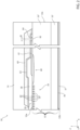
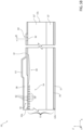
- Figure 1 shows, in lateral cross-sectional view in a (triaxial) cartesian reference system of axes X, Y, Z, a portion of an electronic device (here by way of example a JBS or Junction-Barrier Schottky diode) 1 of a known type.
- an electronic device here by way of example a JBS or Junction-Barrier Schottky diode
- the JBS device 1 comprises a semiconductor body 3, of SiC of an N type, provided with a surface 3a opposite to a surface 3b.
- the semiconductor body includes, for example, a substrate and one or more regions grown epitaxially on the substrate, of an N type and having respective values of doping concentration.
- the JBS device 1 further comprises multiple junction-barrier (JB) elements 9 in the semiconductor body 3, facing the top surface 3a and each including a respective implanted region in the semiconductor body 3, of a P type, and an ohmic contact on the implanted region, at the level of the top surface 3a of the semiconductor body 3.
- JB junction-barrier
- the JBS device 1 further comprises a first metallization 8, which extends over the top surface 3a, in electrical contact with the junction-barrier elements 9 through the respective ohmic contacts.
- the JBS device 1 further comprises an edge-termination region 10 (or protection ring), in particular an implanted region of a P type, which surrounds completely the JB elements 9.
- Schottky diodes 12 are formed at the interface between the anode metallization 8 and the semiconductor body 3, where semiconductor-metal Schottky junctions are formed.
- the region of the MPS device 1 that includes the JB elements 9 and the Schottky diodes 12 i.e., the region contained within the protection ring 10) is an active area 4 of the JBS device 1.
- the JBS device 1 further comprises a second metallization 6, which extends over the bottom surface 3b.
- the first and the second metallizations 8, 6 form, respectively, electrical anode and cathode terminals, which can be biased during use of the JBS device 1.
- An electrically passive region 16 extends outside the edge-termination region 10.
- an insulating layer 18 of insulating or dielectric material, in particular silicon oxide (SiO 2 ).
- the first metallization 8 is in electrical contact with a portion of the edge-termination region 10, where the latter is not covered by the insulating layer 18, and likewise extends partially over the insulating layer 18.
- An interface layer 20, here of silicon nitride (SiN) extends over the first metallization 8 and the insulating layer 18.
- the JBS device 1 comprises a passivation layer 22, in particular of polyimide, which extends over the interface layer 20.
- the interface layer 20 serves as interface between the passivation layer 22 and the underlying layers, here the first metallization 8 and the insulating layer 18.
- the interface layer 20 may be omitted; however, the Applicant has found that the interface layer 20 improves adhesion of the passivation layer 22 to the underlying layers.
- a protection layer 24 of a resin extends over the passivation layer 22, protecting the JBS device 1 when inserted in a package (not illustrated).
- the Applicant has found that in some process conditions of thermo-mechanical or mechanical stress following upon the assembly process, the interface layer 20 has one or more local cracks throughout its thickness, which, at the first metal layer 8, cause the generation of these electrical discharges.
- Patent application US 2021/104445 relates to a silicon carbide (SiC) power device having an improved robustness, in particular in regard to thermomechanical stresses due to thermal cycles.
- Patent US 10,020,373 relates to the construction of a semiconductor device in which a passivation layer is formed over an electrode.
- Patent application US2016/093748 relates to semiconductor devices, and in particular to passivation of such devices.
- an anchoring element of an electronic device an anchoring element, and an electronic device including the anchoring element are provided, as defined in the annexed claims.
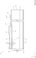
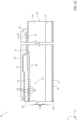
- Figure 2 shows, in lateral cross-sectional view in the same (triaxial) cartesian reference system of axes X, Y, Z of Figure 1 , an electronic device 50 according to an aspect of the present invention.
- the device 50 is a JBS diode, similar to what has been described with reference to Figure 1 .
- the present invention is not limited to this device and finds application also in other types of electronic devices, in particular power devices, such as, for example, MOSFET, IGBT, MPS, Schottky diode, PN diode, PiN diode, etc.
- the electronic device 50 comprises the elements described hereinafter, illustrated with reference to Figure 2 .
- a semiconductor body 53 (e.g., including a substrate 53' and, optionally, one or more epitaxial layers 53" grown thereon), of SiC of an N type or P type (in what follows non-limiting reference will be made only to an N type), is provided with a front surface 53a opposite to a rear surface 53b along the direction of the axis Z.
- the semiconductor body 53 includes, in the example illustrated in Figure 2 , the substrate 53' on which the epitaxial layer 53" has been grown, having the function of drift layer of the electronic device 50, which are both of SiC of an N type (in particular 4H-SiC, however, other polytypes may be used such as, but not exclusively, 2H-SiC, 3C-SiC and 6H-SiC).
- the substrate 53' has a concentration of dopants of an N type comprised between 1 ⁇ 10 19 at/cm 3 and 1 ⁇ 10 22 at/cm 3 and has a thickness, measured along the axis Z between the surfaces 53a and 53b, comprised between 300 ⁇ m and 450 ⁇ m, and in particular equal to approximately 360 ⁇ m.
- the drift layer 53" has a respective dopant concentration lower than the dopant concentration of the substrate and a thickness comprised, for example, between 5 and 15 ⁇ m.
- An ohmic-contact layer 56 (for example, of nickel silicide) extends over the rear surface 53b, and a metallization 57, in this example a cathode metallization, for example, of Ti/NiV/Ag or Ti/NiV/Au, extends over the ohmic-contact region 56.
- a metallization 57 in this example a cathode metallization, for example, of Ti/NiV/Ag or Ti/NiV/Au, extends over the ohmic-contact region 56.
- One or more doped regions 59' of a P type extend in the semiconductor body 53 (in particular, in the drift layer), facing the top surface 53a; each doped region 59' houses a respective ohmic contact (not shown and of a known type) such that each doped region 59' forms a respective junction-barrier (JB) element 59.
- An edge-termination region, or protection ring, 60 in particular a further doped region of a P type, extends in the drift layer, faces the top surface 53a, and surrounds completely (in plan view, in a plane XY defined by the axes X and Y) the JB elements 59.
- the edge-termination region 60 may be omitted.
- An insulating layer 61 (of insulating or dielectric material, e.g., silicon oxide, or TEOS) extends over the top surface 53a so as to surround completely (in view in the plane XY) the JB elements 59 and to overlap partially the protection ring 60 (when present).
- a metallization 58 in this example an anode metallization, for example, of Ti/AlSiCu or Ni/AlSiCu, extends over a portion of the top surface 53a delimited on the outside by the insulating layer 61 (i.e., at the JB elements 59/active area 54) and, partially, over the insulating layer 61.
- polymeric material such as polyamide (e.g., PIX)
- An interface layer 63 here of silicon nitride (SiN), extends over the anode metallization 58 and over the insulating layer 61, and underneath the passivation layer 69.
- the interface layer 63 serves as interface between the passivation layer 69 and the underlying layers, here the metallization 58 and the insulating layer 61, and favours adhesion of the overlying passivation layer 69.
- One or more Schottky diodes 62 are formed at the interface between the semiconductor body 53 and the anode metallization 58, laterally to the doped regions 59'.
- (semiconductor-metal) Schottky junctions are formed by portions of the semiconductor layer 53 in direct electrical contact with respective portions of the anode metallization 58.
- each ohmic contact extending in the respective doped region 59' provides an electrical connection having a value of electrical resistivity lower than the value of electrical resistivity of the doped region 59' that houses it.
- the JB elements 59 are therefore P-i-N diodes.
- the region of the electronic device 50 that includes the JB elements 59 and the Schottky diodes 62 is an active area 54 of the electronic device 50.
- a side surface 53c of the semiconductor body 53 Present outside the active area 54, i.e., beyond the edge-termination region 60, is a side surface 53c of the semiconductor body 53, for example, extending substantially orthogonal to the top surface 53a.
- the side surface 53c is formed following upon a step of dicing or singulation of a SiC wafer wherein a plurality of electronic devices 50 are obtained.
- the dicing step has the function of separating one electronic device 50 from another device 50 of the same wafer. Dicing is performed at a scribe line (not shown) of the SiC wafer from which the electronic device 50 is obtained. This scribe line surrounds at a distance, in the plane XY, the active region 54, the protection ring 60, and the insulating layer 61.
- a protection layer 74 of a resin, such as, for example, bakelite, extends over the passivation layer 69, protecting the electronic device 50 when inserted in a package (not illustrated).
- the passivation layer 69 has an anchoring element 82 that protrudes from the passivation layer 69 (in particular, along the direction of the axis Z) and extends in the insulating layer 61, until it reaches the top surface 53a of the semiconductor body 53.
- the anchoring element 82 anchors and fixes the passivation layer 69 to the insulating layer 61.
- the anchoring element 82 is integral to the passivation layer 69 and, in particular, is an extension of the passivation layer itself.
- the anchoring element 82 therefore extends from the passivation layer without interruptions and without interfaces and is of the same material as the passivation layer. In other words, the anchoring element 82 and the passivation layer 69 form a single or monolithic body.
- the anchoring element 82 extends through an opening 84 made through the interface layer 63.
- the opening 84 has a shape chosen freely in the design stage, for example, a circular, oval, or polygonal shape, with a diameter d 1 of a few microns, for example, between 2 and 5 ⁇ m.
- the anchoring element 82 is formed outside the active area 54, and in particular outside the edge-termination region 60; in other words, the anchoring element 82 is interposed between the edge-termination region 60 and the side surface 53c. In the case where the edge-termination region 60 were not present, the anchoring element 82 is formed outside the active area 54, i.e., between the active area 54 and the side surface 53c in an electrically passive region of the device.
- the anchoring element 82 is patterned so as to fix the passivation layer 69 to the insulating layer 61 and is designed to prevent and/or impede delamination and/or detachment of the passivation layer 69.
- the anchoring element 82 is housed and arranged slotted into a housing or cavity extending in the insulating layer 61 so as to couple the passivation layer 69 and the insulating layer 61 together and render them integral to one another.
- the cavity that houses the anchoring element 82 has a shape complementary to the shape of the anchoring element 82. In other words, the anchoring element 82 fills completely the cavity that houses it.
- the anchoring element 82 has dimensions, in the cross-sectional view of Figure 2 and measured along the axis X, that increase the greater the distance (along the axis Z) from the passivation layer 69.
- the anchoring element 82 has a first dimension, in the cross-sectional view of Figure 2 and measured along the axis X, at the opening 84; the first dimension coincides with the aforementioned diameter d 1 of the opening 84.
- the anchoring element 82 moreover has a second dimension, in the cross-sectional view of Figure 2 and measured along the axis X, within the insulating layer 61.
- the second dimension is greater than the first dimension (for example, but not exclusively, twice as large, i.e., 2 ⁇ d 1 ).
- the anchoring element 82 may have any geometrical shape chosen in the design stage, with dimensions (once again considered in the cross-sectional view of Figure 2 and measured along the axis X) that are variable, but in any case larger than the aforementioned first dimension d 1 at the opening 84.
- the anchoring element 82 may have, in addition or as an alternative to what has been said above with respect to the dimensions along X, a further dimension measured along the axis Y greater than a corresponding dimension (once again measured along the axis Y) of the opening 84.
- the anchoring element 82 extends underneath the opening 84 and has at least one dimension, in the plane XY, larger than a corresponding dimension, in the plane XY, of the opening 84, the anchoring element 82 has the purpose of fixing the passivation layer 69, which is thus constrained in its movements along the axis Z, therefore preventing any delamination or detachment.
- the anchoring element 82 may have, locally, dimensions equal to or smaller than the aforementioned first dimension but, in any case, has at least one portion having a dimension larger than the aforementioned first dimension.
- the portion of the anchoring element 82 that extends within the insulating layer 61 has (in the cross-sectional view and along the axis X) a trapezoidal shape, with the major side directly facing the interface layer 63 and the minor side in contact with the top surface 53a of the semiconductor body.
- the portion of the anchoring element 82 that extends within the insulating layer 61 has (in the cross-sectional view and along the axis X) a rectangular or generically polygonal shape, or an oval shape, or a generically curved or curvilinear shape.
- the anchoring element 82 does not extend through the insulating layer 61 throughout the thickness of the latter, but terminates within the insulating layer 61, at a distance from the top surface 53a of the semiconductor body.
- the shape and dimensions may be chosen similarly to what has been described previously.
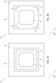
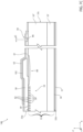
- Figures 3A and 3B show schematically the electronic device 50 in top plan view (in the plane XY), according to respective embodiments.
- the anchoring element 82 extends in the plane XY so as to surround completely the anode metallization 58.
- the anchoring element 82 is annular and defines a closed polygonal shape, and in greater detail a square shape with rounded corners (even though different shapes are also possible, such as a circular shape, a rectangular shape or a generically polygonal or irregular shape).
- the electronic device 50 comprises a plurality of anchoring elements (all of which are similar to the anchoring element 82 described previously and are therefore designated by the same reference number).
- the anchoring elements 82 extend at a distance from one another at the top surface 53a, at respective portions of the top surface 53a, at a distance from one another.
- the view in the plane XY of Figure 3B shows four anchoring elements 82 arranged around the anode metallization 58 so as to be at equal angular distances apart with respect to the anode metallization 58, and in greater detail arranged at corners of an ideal square geometrical shape. Other arrangements are, however, possible.
- two or more anchoring elements 82 may be present set alongside one another.
- two anchoring elements 82 extend in the insulating layer 61 at a mutual distance apart from one another, along the axis X, equal to a few microns or a few tens of microns, for example between 5 ⁇ m and 20 ⁇ m.
- anchoring elements 82 of this plurality of anchoring elements 82 extend within the insulating layer 61 throughout the thickness (along Z) of the latter, or only partially within the insulating layer 61, terminating in the insulating layer 61 without reaching the top surface 53a.
- Steps for manufacturing the electronic device 50 of Figure 2 are described below, with reference to Figures 5A-5C and limitedly to the steps for formation of the anchoring element 82.
- Figures 5A-5C are represented in the same triaxial system as that of Figure 2 .
- a wafer is provided that includes the SiC semiconductor body 53, following upon manufacturing steps designed to form elements of the electronic device 50 described previously (and not discussed here any further) and identified by the same reference numbers.
- the interface layer 63 is selectively etched to form the opening 84.
- a photoresist mask is for example provided and, by lithographic and etching steps per se known, the opening 84 is formed having the shape, dimensions, and location discussed previously.
- the opening 84 extends through the interface layer 63 throughout the thickness of the latter, exposing a respective surface portion of the insulating layer 61.
- an etch of the insulating layer 61 is performed through the opening 84 formed previously.
- the etch is, for example, of a wet type and, if an etching chemistry is used that is selective with respect to the material of the insulating layer 61 (e.g., hydrofluoric acid in the case of silicon oxide), which therefore does not remove the interface layer 63, it is possible to carry out said etch in the absence of a further etching mask. In this case, it is the interface layer 63 that forms the etching mask. Otherwise, it is possible to use a mask similar to the one used for the step of formation of the opening 84.
- Etching of the insulating layer 61 is of an isotropic type and, underneath the interface layer 63, removes the material of the insulating layer both vertically (along Z) and horizontally (in the plane XY).
- the etch is, for example, a timed etch and is interrupted according to the type of shape that it is desired to give to the anchoring element 82.
- etching proceeds until the top surface 53a of the semiconductor body 53 is exposed. As has been said, etching proceeds also laterally (along the axis X). A cavity 86 is thus formed in the insulating layer 61.
- the passivation layer 69 is formed.
- the polymeric material which is liquid or semi-liquid, is applied on the wafer and distributed through spinning on the interface layer 63. During this process, the polymeric material penetrates through the opening 84 and fills completely both the cavity 86 and the opening 84. Then a thermal process is carried out until the polymeric material hardens to form the passivation layer 69 (curing process) and, simultaneously, the anchoring element 82.
- the polymeric material is, for example, polyimide.
- the manufacturing process then continues with subsequent steps to form further elements of the electronic device 50, not described here in detail (for example, the ohmic-contact layer 56 and the cathode metallization 57).
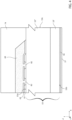
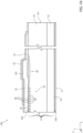
- FIG 6 illustrates an electronic device 100 according to a further embodiment of the present invention.
- the electronic device 100 is represented in the same (triaxial) cartesian reference system of axes X, Y, Z of Figure 1 and Figure 2 .
- the electronic device 100 is a JBS diode, similar to what has been described with reference to Figures 1 and 2 .
- the present invention is not limited to a JBS device and finds application also in other types of electronic devices, in particular power devices, such as MOSFET, IGBT, MPSs, Schottky diode, PN diode, PiN diode, etc.
- the electronic device 100 comprises, in addition to what has been described for the electronic device 50, a further insulating layer 102, in particular of a dielectric or insulating material, such as, for example, silicon oxide.
- a further insulating layer 102 in particular of a dielectric or insulating material, such as, for example, silicon oxide.
- the material of the insulating layer 102 is the same as the one used for the insulating layer 61.
- the insulating layer 102 has, for example, a thickness, along the axis Z, comprised between 0.5 and 2 ⁇ m.
- the insulating layer 102 extends over the anode metallization 58 and the insulating layer 61 laterally to the anode metallization 58.
- the interface layer 63 extends over the insulating layer 102; the passivation layer 69 extends over, and in contact with, the interface layer 63.
- the passivation layer 69 has, similarly to the embodiment of Figure 2 , the anchoring element 82 that protrudes from the passivation layer 69 (in particular, along the direction of the axis Z).
- the anchoring element 82 extends completely within the insulating layer 102 (i.e., throughout the thickness, along Z, of the insulating layer 102) and only partially within the insulating layer 61 (terminating within the insulating layer 61), without reaching the top surface 53a of the semiconductor body 53.
- the anchoring element 82 anchors and fixes the passivation layer 69 both to the insulating layer 102 and to the insulating layer 61.
- the anchoring element 82 is integral to the passivation layer 69 and in particular is an extension of the passivation layer itself.
- the anchoring element 82 therefore extends from the passivation layer without interruptions and without interfaces and is of the same material as the passivation layer.
- the anchoring element 82 and the passivation layer 69 form a single or monolithic body.
- the anchoring element 82 extends through the opening 84 made through the interface layer 63.
- the opening 84 has a shape chosen freely in the design stage, for example a circular, oval, or polygonal shape, with a diameter d 1 equal to a few microns, for example between 2 and 5 ⁇ m.
- the anchoring element 82 is formed outside the active area 54, and in particular outside the edge-termination region 60 and at a distance from the anode metallization 58. In other words, the anchoring element 82 is interposed between the edge-termination region 60 and the side surface 53c. In the case where the edge-termination region 60 is not present, the anchoring element 82 is formed outside the active area 54, i.e., between the active area 54 and the side surface 53c in an electrically passive region of the device and at a distance from the anode metallization 58.
- the anchoring element 82 is housed and arranged slotted into a housing or cavity extending in the insulating layer 102 and in the insulating layer 61 so as to couple the passivation layer 69 and the insulating layers 102 and 61 together and render them integral to one another.
- the cavity that houses the anchoring element 82 has a shape complementary to the shape of the anchoring element 82. In other words, the anchoring element 82 fills completely the cavity that houses it.
- the anchoring element 82 has dimensions that have already been discussed with reference to Figure 2 and are not repeated here for brevity.
- the anchoring element 82 extends exclusively (in part or completely) in the insulating layer 102 (therefore terminating within the insulating layer 102 or at the interface between the insulating layer 102 and the underlying insulating layer 61).
- a time-based etching configured to remove the exact thickness, along Z, of the insulating layer 102, can be used to achieve such result.
- the anchoring element 82 extends throughout the thickness of the insulating layer 102 and throughout the thickness of the insulating layer 61.
- a plurality of anchoring elements 82 may be present, similar to what has been described with reference to Figure 4 .
- One, some or all of the anchoring elements 82 of this plurality of anchoring elements 82 extend exclusively within the insulating layer 102 (and not the insulating layer 61), or throughout the thickness of the insulating layer 102 and throughout the thickness of the insulating layer 61, or throughout the thickness of the insulating layer 102 and partially within the insulating layer 61.
- the insulating layer 102 has the function of forming a further interface between the interface layer 63 and the anode metallization 58, to obtain an electrical insulation at the anode metallization 58 in case of cracking of the interface layer 63.
- the device of Figure 6 may be modified in such a way that the interface layer 63 is absent and the passivation layer 69 extends over, and in contact with, the insulating layer 102.
- Figures 7A-7D show steps for manufacturing the electronic device 100 of Figure 6 limitedly to the steps for formation of the anchoring element 82.
- Figures 7A-7D are represented in the same triaxial system of Figure 6 .
- a wafer is provided that includes the SiC semiconductor body 53, following upon manufacturing steps designed to form elements of the electronic device 100 described previously (and not discussed any further herein) and identified by the same reference numbers.
- a step of deposition of insulating or dielectric material is carried out to form the insulating layer 102.
- This step is carried out, for example, by a CVD process.
- the insulating layer 102 is formed on the entire surface of the wafer and in particular covers completely the anode metallization 50 and the insulating layer 61.
- the interface layer 63 is formed, for example by deposition of a CVD type of silicon nitride.
- the interface layer 63 is formed on the entire surface of the wafer and in particular covers completely the insulating layer 102.
- the interface layer 63 is selectively etched to form the opening 84.
- a photoresist mask is for example provided and, by lithographic and etching steps per se known, the opening 84 is formed having the shape, dimensions, and location discussed previously.
- the opening 84 extends through the interface layer 63 throughout the thickness of the latter, exposing a respective surface portion of the insulating layer 102.
- an etch of the insulating layer 102 is carried out through the opening 84 formed previously.
- the etch is, for example, of a wet type and, if an etching chemistry is used that is selective with respect to the material of the insulating layer 102 (e.g., hydrofluoric acid in the case of silicon oxide), which therefore does not remove the interface layer 63, it is possible to carry out this etch in the absence of a mask. Otherwise, it is possible to use a mask similar to the one used for the step of formation of the opening 84.
- Etching of the insulating layer 102 is of an isotropic type, and, underneath the interface layer 63, the material of the insulating layer 102 is removed both vertically (along Z) and horizontally (in the plane XY).
- the etch is, for example, a timed etch chosen according to the type of shape that it is desired to give to the anchoring element 82. In the embodiment of Figure 7C , etching proceeds until the insulating layer 102 is removed completely, and also proceeds with partial removal of the material of the underlying insulating layer 61.
- the materials of the insulating layer 102 and of the insulating layer 61 can be etched using the same etching chemistry, removal of the portions of the insulating layer 102 and of the insulating layer 61 takes place during the same etching step; otherwise, after having removed the desired portion of the insulating layer 102, the etching chemistry changes to remove the desired portions of the insulating layer 61. As has been said, etching proceeds also laterally (along the axis X) both in the insulating layer 102 and in the insulating layer 61. A cavity 86 is thus formed in the insulating layers 102 and 61.
- the passivation layer 69 is formed.
- the polymeric material which is liquid or semi-liquid, is applied on the wafer and distributed through spinning on the interface layer 63. During this process, the polymeric material penetrates through the opening 84 and fills completely both the cavity 86 and the opening 84. A thermal process is then carried out so that the polymeric material hardens to form the passivation layer 69 (curing process) and, simultaneously, the anchoring element 82.
- the polymeric material is, for example, polyimide.
- the manufacturing process then continues with subsequent steps to form further elements of the electronic device 100, here not described in detail (for example, the ohmic-contact layer 56 and the cathode metallization 57).
- the anchoring element 82 guarantees adhesion of the passivation layer 69, preventing phenomena of delamination. It is thus possible to obtain the passivation layer 69 using polymeric materials, thus guaranteeing high electrical performance of the electronic device 50, 100 (due to the high dielectric strength of the passivation layer 69) and eliminating, at the same time, structural problems linked to the possible detachment of the passivation layer 69 (e.g., following upon thermal cycles or use of the electronic device 50, 100).
- the manufacturing steps described with reference to Figures 5A-5C and 7A-7D make it possible to obtain the electronic device 50 and, respectively, 100 comprising the respective anchoring element 82 starting from a SiC wafer.
- the etch carried out with reference to Figures 5B-5C and 7B-7D is of an isotropic type, and this allows patterning of the cavity thus formed and, consequently, of the anchoring element 82 without limitations deriving from anisotropic etching processes or from the crystallographic orientation of the SiC wafer from which the electronic device 50, 100 is obtained.
- the present disclosure relates, in one aspect, to a method of manufacturing an anchoring element (82) of a passivation layer (69) of an electronic device (50; 100), comprising the steps of:
- the step of providing the passivation material comprises providing the passivation material in liquid or semi-liquid form, so that the passivation material fills the cavity (86).
- the step of providing the passivation material comprises carrying out a step of spinning of the passivation material.
- the manufacturing method above further comprises the step of solidifying, or curing, the passivation material, so that the anchoring element (82) and the passivation layer (69) form a single body or monolithic body.
- removing selective portions of the first insulating layer (61) comprises carrying out an isotropic etching of the first insulating layer (61).
- the interface layer (63) is configured to favour adhesion of the passivation layer (69) with the insulating layer (61).
- forming the anchoring element (82) in the opening (84) and in the cavity (86) comprises constraining the anchoring element (82) underneath the interface layer (63) and within the first insulating layer (61).
- forming the opening (84) comprises forming an etching mask for the first insulating layer (61); the step of removing, through the opening (84), selective portions of the first insulating layer (61) including carrying out a wet etching of the first insulating layer (61).
- said cavity (86) has a volume greater than the volume of the opening (84).
- the passivation material (69) comprises polymeric material.
- the material of the interface layer is silicon nitride.
- said step of forming the cavity (86) comprises: forming the cavity (86) throughout the thickness of the first insulating layer (61); or forming the cavity (86) through part of the thickness of the first insulating layer (61), terminating inside the first insulating layer (61).
- the manufacturing method above further comprises the step of forming a second insulating layer (102) on the first insulating layer (61) and on the layer of metal material (58), underneath the interface layer (63).
- said step of forming the cavity (86) further comprises: forming the cavity (86) exclusively in the second insulating layer (102); or forming the cavity (86) completely through the second insulating layer (102) and in part through the first insulating layer (61), terminating within the first insulating layer (61); or forming the cavity (86) completely through the second insulating layer (102) and the first insulating layer (61).
- said second insulating layer (102) is of the same material as the first insulating layer (61).
- the anchoring element (82) is formed in an electrically passive area of the electronic device, at a distance from the layer of metal material (58).
- the present disclosure relates to an anchoring element (82) for a passivation layer (69) of an electronic device (50; 100), the anchoring element comprising a protrusion that extends, starting from the passivation layer (69), completely through an interface layer (63) and at least in part through an insulating structure (61; 61, 102) arranged underneath the interface layer (63) on a surface (53a) of a semiconductor body (53) of silicon carbide, said protrusion terminating within the insulating structure and forming a single body, or monolithic body, with the passivation layer (69).
- the anchoring element above further comprises: a first portion extending in the interface layer (63) at a first distance from the surface (53a) and having, in a direction parallel to a first axis (X; Y) parallel to the surface (53a), a maximum dimension having a first value (di); and a second portion extending in the insulating structure in structural continuation of the first portion and having, in a direction parallel to the first axis (X; Y), a respective maximum dimension having a second value greater than the first value (d 1 ).
- said second portion of the anchoring element extends in part inside or completely through the insulating structure (61, 102).
- the passivation material (69) comprises polymeric material.
- the anchoring element (82) above extends in an electrically passive area of the electronic device (50; 100) .
- an electronic device comprising: a semiconductor body (53) of silicon carbide; a first insulating layer (61; 102), of a first material, on a surface (53a) of the semiconductor body (53); a layer of metal material (58) extending in part on the surface (53a) of the semiconductor body (53) and in part on the first insulating layer (61); an interface layer (63) on the first insulating layer (61) and on the layer of metal material (58), consisting of a second material different from the first material; a passivation layer (69) on the interface layer (63); and an anchoring element (82) that protrudes from the passivation layer (69) towards the first insulating layer (61; 102) and extends completely through an opening (84) of the interface layer (63) and terminates within the first insulating layer (61; 102), said anchoring element (82) having at least one dimension (d 1 ), in a direction parallel to said surface (53a), greater than
- the anchoring element (82) and the passivation layer (69) form a single body, or monolithic body.
- the interface layer (63) is configured to favour adhesion of the passivation layer (69) with the insulating layer (61).
- the anchoring element (82) is configured to constrain the passivation layer (69) underneath the interface layer (63) and within the first insulating layer (61).
- the anchoring element (82) comprises: a first portion extending in the insulating structure at a first distance from the surface (53a) and having, in a direction parallel to a first axis (X; Y) parallel to the surface (53a), a maximum dimension having a first value (di); and a second portion extending in the insulating structure in structural continuation of the first portion and having, in a direction parallel to the first axis (X; Y), a respective maximum dimension having a second value greater than the first value (di).
- the passivation material (69) comprises polymeric material.
- the material of the interface layer (63) is silicon nitride.
- the anchoring element (82) extends throughout the thickness of the interface layer (63) and of the first insulating layer (61); or throughout the thickness of the interface layer (63) and part of the thickness of the first insulating layer (61), terminating within the first insulating layer (61).
- the electronic device above further comprises a second insulating layer (102) on the first insulating layer (61) and on the layer of metal material (58).
- the anchoring element (82) extends throughout the thickness of the interface layer (63) and: in the second insulating layer (102) terminating within the second insulating layer (102); or completely through the second insulating layer (102) and in part in the first insulating layer (61), terminating within the first insulating layer (61); or completely through the second insulating layer (102) and the first insulating layer (61), terminating at the surface (53a) of the semiconductor body (53) .
- the anchoring element (82) extends in an electrically passive area of the electronic device (50; 100).
Landscapes
- Electrodes Of Semiconductors (AREA)
- Apparatuses And Processes For Manufacturing Resistors (AREA)
Applications Claiming Priority (1)
| Application Number | Priority Date | Filing Date | Title |
|---|---|---|---|
| IT102021000029939A IT202100029939A1 (it) | 2021-11-26 | 2021-11-26 | Metodo di fabbricazione di un elemento di ancoraggio di un dispositivo elettronico basato su sic, elemento di ancoraggio, e dispositivo elettronico |
Publications (3)
| Publication Number | Publication Date |
|---|---|
| EP4191663A1 true EP4191663A1 (de) | 2023-06-07 |
| EP4191663B1 EP4191663B1 (de) | 2025-12-24 |
| EP4191663C0 EP4191663C0 (de) | 2025-12-24 |
Family
ID=79830936
Family Applications (1)
| Application Number | Title | Priority Date | Filing Date |
|---|---|---|---|
| EP22207266.2A Active EP4191663B1 (de) | 2021-11-26 | 2022-11-14 | Verfahren zur herstellung einer sic-basierten elektronischen vorrichtung mit einer passivierungsschicht und einem verankerungselement und einer dadurch hergestellten elektronischen vorrichtung |
Country Status (4)
| Country | Link |
|---|---|
| US (1) | US20230170271A1 (de) |
| EP (1) | EP4191663B1 (de) |
| JP (1) | JP2023079186A (de) |
| IT (1) | IT202100029939A1 (de) |
Cited By (2)
| Publication number | Priority date | Publication date | Assignee | Title |
|---|---|---|---|---|
| CN120565510A (zh) * | 2025-07-30 | 2025-08-29 | 浙江大学 | 一种高压SiC功率器件及其制造方法 |
| DE102024203635A1 (de) * | 2024-04-18 | 2025-10-23 | Infineon Technologies Ag | Halbleiterchip und verfahren zum herstellen desselben |
Families Citing this family (3)
| Publication number | Priority date | Publication date | Assignee | Title |
|---|---|---|---|---|
| CN216413051U (zh) | 2020-09-04 | 2022-04-29 | 意法半导体股份有限公司 | 半导体设备 |
| US20250046665A1 (en) * | 2023-08-01 | 2025-02-06 | Stmicroelectronics International N.V. | Methods for improving passivation layer durability |
| US20250393273A1 (en) * | 2024-06-19 | 2025-12-25 | Stmicroelectronics International N.V. | ELECTRONIC DEVICE BASED ON SiC HAVING IMPROVED ELECTRICAL PERFORMANCES AND MANUFACTURING METHOD |
Citations (3)
| Publication number | Priority date | Publication date | Assignee | Title |
|---|---|---|---|---|
| US20160093748A1 (en) | 2012-10-04 | 2016-03-31 | Cree, Inc. | Passivation for semiconductor devices |
| US10020373B1 (en) | 2017-02-22 | 2018-07-10 | Sanken Electric Co., Ltd. | Semiconductor device |
| US20210104445A1 (en) | 2019-10-02 | 2021-04-08 | Stmicroelectronics S.R.L. | Silicon carbide power device with improved robustness and corresponding manufacturing process |
-
2021
- 2021-11-26 IT IT102021000029939A patent/IT202100029939A1/it unknown
-
2022
- 2022-11-14 EP EP22207266.2A patent/EP4191663B1/de active Active
- 2022-11-16 US US18/056,104 patent/US20230170271A1/en active Pending
- 2022-11-19 JP JP2022185340A patent/JP2023079186A/ja active Pending
Patent Citations (3)
| Publication number | Priority date | Publication date | Assignee | Title |
|---|---|---|---|---|
| US20160093748A1 (en) | 2012-10-04 | 2016-03-31 | Cree, Inc. | Passivation for semiconductor devices |
| US10020373B1 (en) | 2017-02-22 | 2018-07-10 | Sanken Electric Co., Ltd. | Semiconductor device |
| US20210104445A1 (en) | 2019-10-02 | 2021-04-08 | Stmicroelectronics S.R.L. | Silicon carbide power device with improved robustness and corresponding manufacturing process |
Cited By (2)
| Publication number | Priority date | Publication date | Assignee | Title |
|---|---|---|---|---|
| DE102024203635A1 (de) * | 2024-04-18 | 2025-10-23 | Infineon Technologies Ag | Halbleiterchip und verfahren zum herstellen desselben |
| CN120565510A (zh) * | 2025-07-30 | 2025-08-29 | 浙江大学 | 一种高压SiC功率器件及其制造方法 |
Also Published As
| Publication number | Publication date |
|---|---|
| JP2023079186A (ja) | 2023-06-07 |
| EP4191663B1 (de) | 2025-12-24 |
| US20230170271A1 (en) | 2023-06-01 |
| IT202100029939A1 (it) | 2023-05-26 |
| EP4191663C0 (de) | 2025-12-24 |
Similar Documents
| Publication | Publication Date | Title |
|---|---|---|
| EP4191663B1 (de) | Verfahren zur herstellung einer sic-basierten elektronischen vorrichtung mit einer passivierungsschicht und einem verankerungselement und einer dadurch hergestellten elektronischen vorrichtung | |
| JP2003243654A (ja) | 炭化珪素半導体装置およびその製造方法 | |
| EP3800660A1 (de) | Siliciumcarbid-leistungsvorrichtung mit verbesserter robustheit und entsprechendes herstellungsverfahren | |
| US12266530B2 (en) | Manufacturing method of an element of an electronic device having improved reliability, and related element, electronic device and electronic apparatus | |
| EP4187621A1 (de) | Sic-basierte elektronische vorrichtung mit erhöhter robustheit und verfahren zur herstellung der elektronischen vorrichtung | |
| JP2023079186A5 (de) | ||
| EP3965149B1 (de) | Herstellungsverfahren für ein element einer elektronischen vorrichtung mit verbesserter zuverlässigkeit und zugehöriges element, elektronische vorrichtung und elektronische einrichtung | |
| KR20090068148A (ko) | 메사형 반도체 장치 및 그 제조 방법 | |
| US12283534B2 (en) | Power semiconductor devices with improved overcoat adhesion and/or protection | |
| CN219180514U (zh) | 半导体器件和电子器件 | |
| EP4386829A2 (de) | Sic-basierte elektronische vorrichtung mit mehrlagen- und multifunktioneller passivierung und verfahren zur herstellung der elektronischen vorrichtung | |
| CN219591404U (zh) | 电子器件 | |
| EP4668328A1 (de) | Sic-basierte elektronische vorrichtung mit erhöhter robustheit und verfahren zur herstellung der elektronischen vorrichtung | |
| EP4687409A1 (de) | Elektronische vorrichtung mit verbesserter zuverlässigkeit | |
| CN223390546U (zh) | 一种电子器件 | |
| CN221994453U (zh) | 一种电子器件 | |
| EP4669051A1 (de) | Elektronische vorrichtung auf sic-basis mit verbesserten elektrischen leistungen und herstellungsverfahren | |
| JP2026004248A (ja) | 堅牢性が強化されたsicベースの電子デバイス、及び電子デバイスを製造するための方法 | |
| CN116190457A (zh) | 具有增强的鲁棒性的sic基电子器件及制造电子器件的方法 | |
| CN121174533A (zh) | 具有改善的电气性能的基于SiC的电子设备及制造方法 | |
| CN121463498A (zh) | 具有改进的可靠性的电子设备 |
Legal Events
| Date | Code | Title | Description |
|---|---|---|---|
| PUAI | Public reference made under article 153(3) epc to a published international application that has entered the european phase |
Free format text: ORIGINAL CODE: 0009012 |
|
| STAA | Information on the status of an ep patent application or granted ep patent |
Free format text: STATUS: THE APPLICATION HAS BEEN PUBLISHED |
|
| AK | Designated contracting states |
Kind code of ref document: A1 Designated state(s): AL AT BE BG CH CY CZ DE DK EE ES FI FR GB GR HR HU IE IS IT LI LT LU LV MC ME MK MT NL NO PL PT RO RS SE SI SK SM TR |
|
| STAA | Information on the status of an ep patent application or granted ep patent |
Free format text: STATUS: REQUEST FOR EXAMINATION WAS MADE |
|
| 17P | Request for examination filed |
Effective date: 20231128 |
|
| RBV | Designated contracting states (corrected) |
Designated state(s): AL AT BE BG CH CY CZ DE DK EE ES FI FR GB GR HR HU IE IS IT LI LT LU LV MC ME MK MT NL NO PL PT RO RS SE SI SK SM TR |
|
| RIC1 | Information provided on ipc code assigned before grant |
Ipc: H10D 8/60 20250101ALI20250410BHEP Ipc: H10D 62/832 20250101ALI20250410BHEP Ipc: H10D 62/10 20250101ALI20250410BHEP Ipc: H01L 21/56 20060101ALI20250410BHEP Ipc: H01L 23/31 20060101AFI20250410BHEP |
|
| GRAP | Despatch of communication of intention to grant a patent |
Free format text: ORIGINAL CODE: EPIDOSNIGR1 |
|
| STAA | Information on the status of an ep patent application or granted ep patent |
Free format text: STATUS: GRANT OF PATENT IS INTENDED |
|
| INTG | Intention to grant announced |
Effective date: 20250613 |
|
| GRAS | Grant fee paid |
Free format text: ORIGINAL CODE: EPIDOSNIGR3 |
|
| GRAA | (expected) grant |
Free format text: ORIGINAL CODE: 0009210 |
|
| STAA | Information on the status of an ep patent application or granted ep patent |
Free format text: STATUS: THE PATENT HAS BEEN GRANTED |
|
| REG | Reference to a national code |
Ref country code: DE Ref legal event code: R079 Ref document number: 602022027345 Country of ref document: DE Free format text: PREVIOUS MAIN CLASS: H01L0023310000 Ipc: H10W0074100000 |
|
| AK | Designated contracting states |
Kind code of ref document: B1 Designated state(s): AL AT BE BG CH CY CZ DE DK EE ES FI FR GB GR HR HU IE IS IT LI LT LU LV MC ME MK MT NL NO PL PT RO RS SE SI SK SM TR |
|
| REG | Reference to a national code |
Ref country code: CH Ref legal event code: F10 Free format text: ST27 STATUS EVENT CODE: U-0-0-F10-F00 (AS PROVIDED BY THE NATIONAL OFFICE) Effective date: 20251224 Ref country code: GB Ref legal event code: FG4D |
|
| REG | Reference to a national code |
Ref country code: DE Ref legal event code: R096 Ref document number: 602022027345 Country of ref document: DE |
|
| U01 | Request for unitary effect filed |
Effective date: 20251224 |
|
| U07 | Unitary effect registered |
Designated state(s): AT BE BG DE DK EE FI FR IT LT LU LV MT NL PT RO SE SI Effective date: 20260109 |
|
| PG25 | Lapsed in a contracting state [announced via postgrant information from national office to epo] |
Ref country code: NO Free format text: LAPSE BECAUSE OF FAILURE TO SUBMIT A TRANSLATION OF THE DESCRIPTION OR TO PAY THE FEE WITHIN THE PRESCRIBED TIME-LIMIT Effective date: 20260324 |
|
| PG25 | Lapsed in a contracting state [announced via postgrant information from national office to epo] |
Ref country code: HR Free format text: LAPSE BECAUSE OF FAILURE TO SUBMIT A TRANSLATION OF THE DESCRIPTION OR TO PAY THE FEE WITHIN THE PRESCRIBED TIME-LIMIT Effective date: 20251224 |
|
| PG25 | Lapsed in a contracting state [announced via postgrant information from national office to epo] |
Ref country code: RS Free format text: LAPSE BECAUSE OF FAILURE TO SUBMIT A TRANSLATION OF THE DESCRIPTION OR TO PAY THE FEE WITHIN THE PRESCRIBED TIME-LIMIT Effective date: 20260324 |