EP4181189A1 - Semiconductor structure and preparation method therefor - Google Patents
Semiconductor structure and preparation method therefor Download PDFInfo
- Publication number
- EP4181189A1 EP4181189A1 EP21927490.9A EP21927490A EP4181189A1 EP 4181189 A1 EP4181189 A1 EP 4181189A1 EP 21927490 A EP21927490 A EP 21927490A EP 4181189 A1 EP4181189 A1 EP 4181189A1
- Authority
- EP
- European Patent Office
- Prior art keywords
- adhesive layer
- semiconductor structure
- hole slot
- layer
- die
- Prior art date
- Legal status (The legal status is an assumption and is not a legal conclusion. Google has not performed a legal analysis and makes no representation as to the accuracy of the status listed.)
- Granted
Links
Images



Classifications
-
- H—ELECTRICITY
- H10—SEMICONDUCTOR DEVICES; ELECTRIC SOLID-STATE DEVICES NOT OTHERWISE PROVIDED FOR
- H10W—GENERIC PACKAGES, INTERCONNECTIONS, CONNECTORS OR OTHER CONSTRUCTIONAL DETAILS OF DEVICES COVERED BY CLASS H10
- H10W72/00—Interconnections or connectors in packages
- H10W72/20—Bump connectors, e.g. solder bumps or copper pillars; Dummy bumps; Thermal bumps
-
- H—ELECTRICITY
- H10—SEMICONDUCTOR DEVICES; ELECTRIC SOLID-STATE DEVICES NOT OTHERWISE PROVIDED FOR
- H10W—GENERIC PACKAGES, INTERCONNECTIONS, CONNECTORS OR OTHER CONSTRUCTIONAL DETAILS OF DEVICES COVERED BY CLASS H10
- H10W72/00—Interconnections or connectors in packages
- H10W72/30—Die-attach connectors
-
- H—ELECTRICITY
- H10—SEMICONDUCTOR DEVICES; ELECTRIC SOLID-STATE DEVICES NOT OTHERWISE PROVIDED FOR
- H10W—GENERIC PACKAGES, INTERCONNECTIONS, CONNECTORS OR OTHER CONSTRUCTIONAL DETAILS OF DEVICES COVERED BY CLASS H10
- H10W72/00—Interconnections or connectors in packages
- H10W72/071—Connecting or disconnecting
-
- H—ELECTRICITY
- H10—SEMICONDUCTOR DEVICES; ELECTRIC SOLID-STATE DEVICES NOT OTHERWISE PROVIDED FOR
- H10W—GENERIC PACKAGES, INTERCONNECTIONS, CONNECTORS OR OTHER CONSTRUCTIONAL DETAILS OF DEVICES COVERED BY CLASS H10
- H10W72/00—Interconnections or connectors in packages
- H10W72/30—Die-attach connectors
- H10W72/331—Shapes of die-attach connectors
- H10W72/334—Cross-sectional shape, i.e. in side view
-
- H—ELECTRICITY
- H10—SEMICONDUCTOR DEVICES; ELECTRIC SOLID-STATE DEVICES NOT OTHERWISE PROVIDED FOR
- H10W—GENERIC PACKAGES, INTERCONNECTIONS, CONNECTORS OR OTHER CONSTRUCTIONAL DETAILS OF DEVICES COVERED BY CLASS H10
- H10W72/00—Interconnections or connectors in packages
- H10W72/01—Manufacture or treatment
- H10W72/013—Manufacture or treatment of die-attach connectors
- H10W72/01308—Manufacture or treatment of die-attach connectors using permanent auxiliary members, e.g. using alignment marks
-
- H—ELECTRICITY
- H10—SEMICONDUCTOR DEVICES; ELECTRIC SOLID-STATE DEVICES NOT OTHERWISE PROVIDED FOR
- H10W—GENERIC PACKAGES, INTERCONNECTIONS, CONNECTORS OR OTHER CONSTRUCTIONAL DETAILS OF DEVICES COVERED BY CLASS H10
- H10W72/00—Interconnections or connectors in packages
- H10W72/01—Manufacture or treatment
- H10W72/013—Manufacture or treatment of die-attach connectors
- H10W72/01321—Manufacture or treatment of die-attach connectors using local deposition
- H10W72/01323—Manufacture or treatment of die-attach connectors using local deposition in liquid form, e.g. by dispensing droplets or by screen printing
-
- H—ELECTRICITY
- H10—SEMICONDUCTOR DEVICES; ELECTRIC SOLID-STATE DEVICES NOT OTHERWISE PROVIDED FOR
- H10W—GENERIC PACKAGES, INTERCONNECTIONS, CONNECTORS OR OTHER CONSTRUCTIONAL DETAILS OF DEVICES COVERED BY CLASS H10
- H10W72/00—Interconnections or connectors in packages
- H10W72/01—Manufacture or treatment
- H10W72/013—Manufacture or treatment of die-attach connectors
- H10W72/01321—Manufacture or treatment of die-attach connectors using local deposition
- H10W72/01325—Manufacture or treatment of die-attach connectors using local deposition in solid form
-
- H—ELECTRICITY
- H10—SEMICONDUCTOR DEVICES; ELECTRIC SOLID-STATE DEVICES NOT OTHERWISE PROVIDED FOR
- H10W—GENERIC PACKAGES, INTERCONNECTIONS, CONNECTORS OR OTHER CONSTRUCTIONAL DETAILS OF DEVICES COVERED BY CLASS H10
- H10W72/00—Interconnections or connectors in packages
- H10W72/01—Manufacture or treatment
- H10W72/013—Manufacture or treatment of die-attach connectors
- H10W72/01351—Changing the shapes of die-attach connectors
- H10W72/01355—Changing the shapes of die-attach connectors by use of masks
-
- H—ELECTRICITY
- H10—SEMICONDUCTOR DEVICES; ELECTRIC SOLID-STATE DEVICES NOT OTHERWISE PROVIDED FOR
- H10W—GENERIC PACKAGES, INTERCONNECTIONS, CONNECTORS OR OTHER CONSTRUCTIONAL DETAILS OF DEVICES COVERED BY CLASS H10
- H10W72/00—Interconnections or connectors in packages
- H10W72/01—Manufacture or treatment
- H10W72/013—Manufacture or treatment of die-attach connectors
- H10W72/01361—Chemical or physical modification, e.g. by sintering or anodisation
-
- H—ELECTRICITY
- H10—SEMICONDUCTOR DEVICES; ELECTRIC SOLID-STATE DEVICES NOT OTHERWISE PROVIDED FOR
- H10W—GENERIC PACKAGES, INTERCONNECTIONS, CONNECTORS OR OTHER CONSTRUCTIONAL DETAILS OF DEVICES COVERED BY CLASS H10
- H10W72/00—Interconnections or connectors in packages
- H10W72/01—Manufacture or treatment
- H10W72/015—Manufacture or treatment of bond wires
- H10W72/01515—Forming coatings
-
- H—ELECTRICITY
- H10—SEMICONDUCTOR DEVICES; ELECTRIC SOLID-STATE DEVICES NOT OTHERWISE PROVIDED FOR
- H10W—GENERIC PACKAGES, INTERCONNECTIONS, CONNECTORS OR OTHER CONSTRUCTIONAL DETAILS OF DEVICES COVERED BY CLASS H10
- H10W72/00—Interconnections or connectors in packages
- H10W72/071—Connecting or disconnecting
- H10W72/0711—Apparatus therefor
- H10W72/07141—Means for applying energy, e.g. ovens or lasers
-
- H—ELECTRICITY
- H10—SEMICONDUCTOR DEVICES; ELECTRIC SOLID-STATE DEVICES NOT OTHERWISE PROVIDED FOR
- H10W—GENERIC PACKAGES, INTERCONNECTIONS, CONNECTORS OR OTHER CONSTRUCTIONAL DETAILS OF DEVICES COVERED BY CLASS H10
- H10W72/00—Interconnections or connectors in packages
- H10W72/071—Connecting or disconnecting
- H10W72/073—Connecting or disconnecting of die-attach connectors
-
- H—ELECTRICITY
- H10—SEMICONDUCTOR DEVICES; ELECTRIC SOLID-STATE DEVICES NOT OTHERWISE PROVIDED FOR
- H10W—GENERIC PACKAGES, INTERCONNECTIONS, CONNECTORS OR OTHER CONSTRUCTIONAL DETAILS OF DEVICES COVERED BY CLASS H10
- H10W72/00—Interconnections or connectors in packages
- H10W72/071—Connecting or disconnecting
- H10W72/073—Connecting or disconnecting of die-attach connectors
- H10W72/07331—Connecting techniques
-
- H—ELECTRICITY
- H10—SEMICONDUCTOR DEVICES; ELECTRIC SOLID-STATE DEVICES NOT OTHERWISE PROVIDED FOR
- H10W—GENERIC PACKAGES, INTERCONNECTIONS, CONNECTORS OR OTHER CONSTRUCTIONAL DETAILS OF DEVICES COVERED BY CLASS H10
- H10W72/00—Interconnections or connectors in packages
- H10W72/071—Connecting or disconnecting
- H10W72/073—Connecting or disconnecting of die-attach connectors
- H10W72/07331—Connecting techniques
- H10W72/07332—Compression bonding, e.g. thermocompression bonding
-
- H—ELECTRICITY
- H10—SEMICONDUCTOR DEVICES; ELECTRIC SOLID-STATE DEVICES NOT OTHERWISE PROVIDED FOR
- H10W—GENERIC PACKAGES, INTERCONNECTIONS, CONNECTORS OR OTHER CONSTRUCTIONAL DETAILS OF DEVICES COVERED BY CLASS H10
- H10W72/00—Interconnections or connectors in packages
- H10W72/071—Connecting or disconnecting
- H10W72/073—Connecting or disconnecting of die-attach connectors
- H10W72/07331—Connecting techniques
- H10W72/07337—Connecting techniques using a polymer adhesive, e.g. an adhesive based on silicone or epoxy
- H10W72/07338—Connecting techniques using a polymer adhesive, e.g. an adhesive based on silicone or epoxy hardening the adhesive by curing, e.g. thermosetting
-
- H—ELECTRICITY
- H10—SEMICONDUCTOR DEVICES; ELECTRIC SOLID-STATE DEVICES NOT OTHERWISE PROVIDED FOR
- H10W—GENERIC PACKAGES, INTERCONNECTIONS, CONNECTORS OR OTHER CONSTRUCTIONAL DETAILS OF DEVICES COVERED BY CLASS H10
- H10W72/00—Interconnections or connectors in packages
- H10W72/071—Connecting or disconnecting
- H10W72/073—Connecting or disconnecting of die-attach connectors
- H10W72/07351—Connecting or disconnecting of die-attach connectors characterised by changes in properties of the die-attach connectors during connecting
- H10W72/07352—Connecting or disconnecting of die-attach connectors characterised by changes in properties of the die-attach connectors during connecting changes in structures or sizes
-
- H—ELECTRICITY
- H10—SEMICONDUCTOR DEVICES; ELECTRIC SOLID-STATE DEVICES NOT OTHERWISE PROVIDED FOR
- H10W—GENERIC PACKAGES, INTERCONNECTIONS, CONNECTORS OR OTHER CONSTRUCTIONAL DETAILS OF DEVICES COVERED BY CLASS H10
- H10W72/00—Interconnections or connectors in packages
- H10W72/071—Connecting or disconnecting
- H10W72/073—Connecting or disconnecting of die-attach connectors
- H10W72/07351—Connecting or disconnecting of die-attach connectors characterised by changes in properties of the die-attach connectors during connecting
- H10W72/07354—Connecting or disconnecting of die-attach connectors characterised by changes in properties of the die-attach connectors during connecting changes in dispositions
-
- H—ELECTRICITY
- H10—SEMICONDUCTOR DEVICES; ELECTRIC SOLID-STATE DEVICES NOT OTHERWISE PROVIDED FOR
- H10W—GENERIC PACKAGES, INTERCONNECTIONS, CONNECTORS OR OTHER CONSTRUCTIONAL DETAILS OF DEVICES COVERED BY CLASS H10
- H10W72/00—Interconnections or connectors in packages
- H10W72/071—Connecting or disconnecting
- H10W72/075—Connecting or disconnecting of bond wires
-
- H—ELECTRICITY
- H10—SEMICONDUCTOR DEVICES; ELECTRIC SOLID-STATE DEVICES NOT OTHERWISE PROVIDED FOR
- H10W—GENERIC PACKAGES, INTERCONNECTIONS, CONNECTORS OR OTHER CONSTRUCTIONAL DETAILS OF DEVICES COVERED BY CLASS H10
- H10W72/00—Interconnections or connectors in packages
- H10W72/30—Die-attach connectors
- H10W72/321—Structures or relative sizes of die-attach connectors
-
- H—ELECTRICITY
- H10—SEMICONDUCTOR DEVICES; ELECTRIC SOLID-STATE DEVICES NOT OTHERWISE PROVIDED FOR
- H10W—GENERIC PACKAGES, INTERCONNECTIONS, CONNECTORS OR OTHER CONSTRUCTIONAL DETAILS OF DEVICES COVERED BY CLASS H10
- H10W72/00—Interconnections or connectors in packages
- H10W72/30—Die-attach connectors
- H10W72/321—Structures or relative sizes of die-attach connectors
- H10W72/322—Multilayered die-attach connectors, e.g. a coating on a top surface of a core
-
- H—ELECTRICITY
- H10—SEMICONDUCTOR DEVICES; ELECTRIC SOLID-STATE DEVICES NOT OTHERWISE PROVIDED FOR
- H10W—GENERIC PACKAGES, INTERCONNECTIONS, CONNECTORS OR OTHER CONSTRUCTIONAL DETAILS OF DEVICES COVERED BY CLASS H10
- H10W72/00—Interconnections or connectors in packages
- H10W72/30—Die-attach connectors
- H10W72/321—Structures or relative sizes of die-attach connectors
- H10W72/324—Die-attach connectors having multiple side-by-side cores
-
- H—ELECTRICITY
- H10—SEMICONDUCTOR DEVICES; ELECTRIC SOLID-STATE DEVICES NOT OTHERWISE PROVIDED FOR
- H10W—GENERIC PACKAGES, INTERCONNECTIONS, CONNECTORS OR OTHER CONSTRUCTIONAL DETAILS OF DEVICES COVERED BY CLASS H10
- H10W72/00—Interconnections or connectors in packages
- H10W72/30—Die-attach connectors
- H10W72/321—Structures or relative sizes of die-attach connectors
- H10W72/327—Multiple die-attach connectors having different sizes
-
- H—ELECTRICITY
- H10—SEMICONDUCTOR DEVICES; ELECTRIC SOLID-STATE DEVICES NOT OTHERWISE PROVIDED FOR
- H10W—GENERIC PACKAGES, INTERCONNECTIONS, CONNECTORS OR OTHER CONSTRUCTIONAL DETAILS OF DEVICES COVERED BY CLASS H10
- H10W72/00—Interconnections or connectors in packages
- H10W72/30—Die-attach connectors
- H10W72/321—Structures or relative sizes of die-attach connectors
- H10W72/328—Multiple die-attach connectors having different structures
-
- H—ELECTRICITY
- H10—SEMICONDUCTOR DEVICES; ELECTRIC SOLID-STATE DEVICES NOT OTHERWISE PROVIDED FOR
- H10W—GENERIC PACKAGES, INTERCONNECTIONS, CONNECTORS OR OTHER CONSTRUCTIONAL DETAILS OF DEVICES COVERED BY CLASS H10
- H10W72/00—Interconnections or connectors in packages
- H10W72/30—Die-attach connectors
- H10W72/331—Shapes of die-attach connectors
-
- H—ELECTRICITY
- H10—SEMICONDUCTOR DEVICES; ELECTRIC SOLID-STATE DEVICES NOT OTHERWISE PROVIDED FOR
- H10W—GENERIC PACKAGES, INTERCONNECTIONS, CONNECTORS OR OTHER CONSTRUCTIONAL DETAILS OF DEVICES COVERED BY CLASS H10
- H10W72/00—Interconnections or connectors in packages
- H10W72/30—Die-attach connectors
- H10W72/331—Shapes of die-attach connectors
- H10W72/332—Plan-view shape, i.e. in top view
-
- H—ELECTRICITY
- H10—SEMICONDUCTOR DEVICES; ELECTRIC SOLID-STATE DEVICES NOT OTHERWISE PROVIDED FOR
- H10W—GENERIC PACKAGES, INTERCONNECTIONS, CONNECTORS OR OTHER CONSTRUCTIONAL DETAILS OF DEVICES COVERED BY CLASS H10
- H10W72/00—Interconnections or connectors in packages
- H10W72/30—Die-attach connectors
- H10W72/341—Dispositions of die-attach connectors, e.g. layouts
- H10W72/342—Dispositions of die-attach connectors, e.g. layouts relative to the surface, e.g. recessed, protruding
-
- H—ELECTRICITY
- H10—SEMICONDUCTOR DEVICES; ELECTRIC SOLID-STATE DEVICES NOT OTHERWISE PROVIDED FOR
- H10W—GENERIC PACKAGES, INTERCONNECTIONS, CONNECTORS OR OTHER CONSTRUCTIONAL DETAILS OF DEVICES COVERED BY CLASS H10
- H10W72/00—Interconnections or connectors in packages
- H10W72/30—Die-attach connectors
- H10W72/341—Dispositions of die-attach connectors, e.g. layouts
- H10W72/347—Dispositions of multiple die-attach connectors
-
- H—ELECTRICITY
- H10—SEMICONDUCTOR DEVICES; ELECTRIC SOLID-STATE DEVICES NOT OTHERWISE PROVIDED FOR
- H10W—GENERIC PACKAGES, INTERCONNECTIONS, CONNECTORS OR OTHER CONSTRUCTIONAL DETAILS OF DEVICES COVERED BY CLASS H10
- H10W72/00—Interconnections or connectors in packages
- H10W72/30—Die-attach connectors
- H10W72/351—Materials of die-attach connectors
- H10W72/353—Materials of die-attach connectors not comprising solid metals or solid metalloids, e.g. ceramics
- H10W72/354—Materials of die-attach connectors not comprising solid metals or solid metalloids, e.g. ceramics comprising polymers
-
- H—ELECTRICITY
- H10—SEMICONDUCTOR DEVICES; ELECTRIC SOLID-STATE DEVICES NOT OTHERWISE PROVIDED FOR
- H10W—GENERIC PACKAGES, INTERCONNECTIONS, CONNECTORS OR OTHER CONSTRUCTIONAL DETAILS OF DEVICES COVERED BY CLASS H10
- H10W72/00—Interconnections or connectors in packages
- H10W72/30—Die-attach connectors
- H10W72/351—Materials of die-attach connectors
- H10W72/355—Materials of die-attach connectors of outermost layers of multilayered die-attach connectors, e.g. material of a coating
-
- H—ELECTRICITY
- H10—SEMICONDUCTOR DEVICES; ELECTRIC SOLID-STATE DEVICES NOT OTHERWISE PROVIDED FOR
- H10W—GENERIC PACKAGES, INTERCONNECTIONS, CONNECTORS OR OTHER CONSTRUCTIONAL DETAILS OF DEVICES COVERED BY CLASS H10
- H10W72/00—Interconnections or connectors in packages
- H10W72/50—Bond wires
- H10W72/551—Materials of bond wires
-
- H—ELECTRICITY
- H10—SEMICONDUCTOR DEVICES; ELECTRIC SOLID-STATE DEVICES NOT OTHERWISE PROVIDED FOR
- H10W—GENERIC PACKAGES, INTERCONNECTIONS, CONNECTORS OR OTHER CONSTRUCTIONAL DETAILS OF DEVICES COVERED BY CLASS H10
- H10W72/00—Interconnections or connectors in packages
- H10W72/851—Dispositions of multiple connectors or interconnections
- H10W72/853—On the same surface
- H10W72/865—Die-attach connectors and bond wires
-
- H—ELECTRICITY
- H10—SEMICONDUCTOR DEVICES; ELECTRIC SOLID-STATE DEVICES NOT OTHERWISE PROVIDED FOR
- H10W—GENERIC PACKAGES, INTERCONNECTIONS, CONNECTORS OR OTHER CONSTRUCTIONAL DETAILS OF DEVICES COVERED BY CLASS H10
- H10W72/00—Interconnections or connectors in packages
- H10W72/851—Dispositions of multiple connectors or interconnections
- H10W72/874—On different surfaces
- H10W72/884—Die-attach connectors and bond wires
-
- H—ELECTRICITY
- H10—SEMICONDUCTOR DEVICES; ELECTRIC SOLID-STATE DEVICES NOT OTHERWISE PROVIDED FOR
- H10W—GENERIC PACKAGES, INTERCONNECTIONS, CONNECTORS OR OTHER CONSTRUCTIONAL DETAILS OF DEVICES COVERED BY CLASS H10
- H10W74/00—Encapsulations, e.g. protective coatings
-
- H—ELECTRICITY
- H10—SEMICONDUCTOR DEVICES; ELECTRIC SOLID-STATE DEVICES NOT OTHERWISE PROVIDED FOR
- H10W—GENERIC PACKAGES, INTERCONNECTIONS, CONNECTORS OR OTHER CONSTRUCTIONAL DETAILS OF DEVICES COVERED BY CLASS H10
- H10W90/00—Package configurations
-
- H—ELECTRICITY
- H10—SEMICONDUCTOR DEVICES; ELECTRIC SOLID-STATE DEVICES NOT OTHERWISE PROVIDED FOR
- H10W—GENERIC PACKAGES, INTERCONNECTIONS, CONNECTORS OR OTHER CONSTRUCTIONAL DETAILS OF DEVICES COVERED BY CLASS H10
- H10W90/00—Package configurations
- H10W90/701—Package configurations characterised by the relative positions of pads or connectors relative to package parts
- H10W90/731—Package configurations characterised by the relative positions of pads or connectors relative to package parts of die-attach connectors
- H10W90/732—Package configurations characterised by the relative positions of pads or connectors relative to package parts of die-attach connectors between stacked chips
-
- H—ELECTRICITY
- H10—SEMICONDUCTOR DEVICES; ELECTRIC SOLID-STATE DEVICES NOT OTHERWISE PROVIDED FOR
- H10W—GENERIC PACKAGES, INTERCONNECTIONS, CONNECTORS OR OTHER CONSTRUCTIONAL DETAILS OF DEVICES COVERED BY CLASS H10
- H10W90/00—Package configurations
- H10W90/701—Package configurations characterised by the relative positions of pads or connectors relative to package parts
- H10W90/731—Package configurations characterised by the relative positions of pads or connectors relative to package parts of die-attach connectors
- H10W90/734—Package configurations characterised by the relative positions of pads or connectors relative to package parts of die-attach connectors between a chip and a stacked insulating package substrate, interposer or RDL
-
- H—ELECTRICITY
- H10—SEMICONDUCTOR DEVICES; ELECTRIC SOLID-STATE DEVICES NOT OTHERWISE PROVIDED FOR
- H10W—GENERIC PACKAGES, INTERCONNECTIONS, CONNECTORS OR OTHER CONSTRUCTIONAL DETAILS OF DEVICES COVERED BY CLASS H10
- H10W90/00—Package configurations
- H10W90/701—Package configurations characterised by the relative positions of pads or connectors relative to package parts
- H10W90/751—Package configurations characterised by the relative positions of pads or connectors relative to package parts of bond wires
- H10W90/754—Package configurations characterised by the relative positions of pads or connectors relative to package parts of bond wires between a chip and a stacked insulating package substrate, interposer or RDL
Definitions
- the present disclosure relates to the technical field of semiconductors, and in particular to a semiconductor structure and a manufacturing method thereof.
- a die, an adhesive layer and a solder mask (SR for short, alias "green mask”) on a substrate are in direct contact with each other.
- the substrate (including the solder mask) and the die are designed thinner and thinner.
- TC reliability temperature cycling reliability
- One aspect of the embodiments of the present disclosure provides a semiconductor structure, including a substrate, a die and a first adhesive layer, wherein a surface of the substrate is provided with an insulation layer; the die is arranged on a surface of the insulation layer via the first adhesive layer; the insulation layer is provided with at least one hole slot; a position of the at least one hole slot corresponds to at least a part of an edge of the first adhesive layer; a second adhesive layer is arranged in the at least one hole slot; at least a part of a surface of the second adhesive layer is connected with the first adhesive layer; and an elasticity modulus of the second adhesive layer is smaller than an elasticity modulus of the first adhesive layer.
- Another aspect of the embodiments of the present disclosure provides a method of manufacturing a semiconductor structure, including: providing a substrate, wherein a surface of the substrate is provided with an insulation layer; forming at least one hole slot which runs through the insulation layer on the insulation layer; forming a second adhesive layer in the at least one hole slot; arranging a die on a surface of the insulation layer via a first adhesive layer, wherein a position of the at least one hole slot corresponds to at least a part of an edge of the first adhesive layer, at least a part of a surface of the second adhesive layer is connected with the first adhesive layer; and an elasticity modulus of the second adhesive layer is smaller than an elasticity modulus of the first adhesive layer; and forming a packaging layer on the surface of the insulation layer, wherein the die and the first adhesive layer are packaged in the packaging layer.
- FIG. 11 representatively shows a schematic structure of a semiconductor structure proposed by the present disclosure.
- the semiconductor structure proposed by the present disclosure is described by taking its application to a packaging structure of a memory thin die stack as an example. It is understandable for those skilled in the art that, in order to apply the relevant design of the present disclosure to other types of semiconductor structures, various modifications, additions, substitutions, deletions or other changes may be made to the following specific embodiments, but such changes are still within the scope of the principle of the semiconductor structure proposed by the present disclosure.
- the semiconductor structure proposed by the present disclosure mainly includes a substrate 110, a die 130 and a first adhesive layer 140.
- a surface of the substrate 110 is provided with an insulation layer 120.
- the die 130 is arranged on a surface of the insulation layer 120 via the first adhesive layer 140.
- the insulation layer 120 is provided with at least one hole slot 121, and a position of the at least one hole slot 121 corresponds to an edge of the first adhesive layer 140.
- a second adhesive layer 122 is arranged in the at least one hole slot 121, and at least a part of a surface of the second adhesive layer 122 is connected with the first adhesive layer 140.
- an elasticity modulus of the second adhesive layer 122 is smaller than an elasticity modulus of the first adhesive layer 140.
- the semiconductor structure proposed by the present disclosure can optimize the stress distribution of an edge where the die 130 is connected with the substrate 110 (including the insulation layer 120 arranged on the surface of the substrate 110), such that the semiconductor structure is difficult to generate crack at the edge where the die 130 is connected with the substrate 110 during bending or deformation.
- the at least one hole slot 121 may run through the insulation layer 120.
- the at least one hole slot 121 may also not run through the insulation layer 120, for example, the at least one hole slot 121 is only opened on an upper surface of the insulation layer 120.
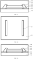
- FIG. 5 representatively shows a top view of the semiconductor structure in forming the at least one hole slot 121
- one hole slot of the at least one hole slot 121 may approximately be an annular closed structure, such that the hole slot of the at least one hole slot 121 corresponds to the whole edge of the first adhesive layer 140.
- the semiconductor structure proposed by the present disclosure can optimize the stress distribution of the whole position of the edge where the die 130 is connected with the substrate 110, such that the whole edge where the die 130 is connected with the substrate 110 is difficult to generate crack.
- the first adhesive layer 140 may be approximately rectangular and the edge of the first adhesive layer 140 has four side edges.
- the hole slot of the at least one hole slot 121 may be approximately arranged in a form of a rectangular ring.
- the hole slot of the at least one hole slot 121 may be arranged in corresponding forms of a circular ring, a triangular ring, a trapezoidal ring and the like, which is not limited to the embodiment.
- an outer side edge of an orthographic projection of the at least one hole slot 121 may be located outside an edge of an orthographic projection of the first adhesive layer 140. Accordingly, the second adhesive layer 122 arranged in the at least one hole slot 121 can extend to an outer side of the edge of the first adhesive layer 140, such that the present disclosure can optimize the stress distribution of a part of a region, located on the outer side of the edge of the first adhesive layer 140, of the substrate 110, thereby further preventing crack of a relevant region.
- FIG. 9 representatively shows a top view of the semiconductor structure in arranging the die 130, and in the embodiment, a notch width d1 of the at least one hole slot 121 may be 5%-10% of a width d2 of the first adhesive layer 140, for example, 5%, 6.5%, 8% and 10%. Accordingly, the present disclosure selects a width proportion of the hole 121 to the first adhesive layer 140 as a reasonable scope, thereby preventing the die 130 from overall viscosity inefficiency due to excessive notch width d1 of the at least one hole slot 121, and preventing the condition that the effects of better stress distribution optimization and crack prevention cannot be realized due to too small notch width d1 when the semiconductor structure deforms.
- the notch width d1 of the at least one hole slot 121 may be smaller than 5% or greater than 10% of the width d2 of the first adhesive layer 140, for example, 4.5%, 11% and the like, which is not limited to the embodiment.
- the elasticity modulus of the second adhesive layer 122 may be smaller than the elasticity modulus of the insulation layer 120. Accordingly, a corresponding position (for example, a position adjoining the at least one hole slot 121, namely, a position corresponding to the edge of the first adhesive layer 140) of the insulation layer 120 may be difficult to generate crack.
- the elasticity modulus of the second adhesive layer 122 may also be equal to or greater than the elasticity modulus of the insulation layer 120, which is not limited to the embodiment.
- the elasticity modulus of the second adhesive layer 122 may be smaller than the elasticity modulus of the die 130. Accordingly, a corresponding position (for example, an edge position) of the die 130 may be difficult to generate crack.
- the elasticity modulus of the second adhesive layer 122 may also be equal to or greater than the elasticity modulus of the die 130, which is not limited to the embodiment.
- a coefficient of thermal expansion of the second adhesive layer 122 may be smaller than a coefficient of thermal expansion of the first adhesive layer 140. Accordingly, when the semiconductor structure is heated to deform, as the second adhesive layer 122 has a lower coefficient of thermal expansion relative to the first adhesive layer 140, the first adhesive layer 140 can be prevented from crack caused by generating, by the second adhesive layer, same or even larger expansive deformation as the first adhesive layer 140.
- the coefficient of thermal expansion of the second adhesive layer 122 may also be greater than or equal to the coefficient of thermal expansion of the first adhesive layer 140, which is not limited to the embodiment.
- the coefficient of thermal expansion of the second adhesive layer 122 may also be smaller than the coefficient of thermal expansion of the insulation layer 120. Accordingly, when the semiconductor structure is heated to deform, as the second adhesive layer 122 has a lower coefficient of thermal expansion relative to the insulation layer 120, the insulation layer 120 may be prevented from crack caused by generating, by the second adhesive layer 122, same or even larger expansive deformation as the insulation layer 120.
- the coefficient of thermal expansion of the second adhesive layer 122 may also be greater than or equal to the coefficient of thermal expansion of the insulation layer 120, which is not limited to the embodiment.
- the coefficient of thermal expansion of the second adhesive layer 122 may also be smaller than the coefficient of thermal expansion of the die 130. Accordingly, when the semiconductor structure is heated to deform, as the second adhesive layer 122 has a lower coefficient of thermal expansion relative to the die 130, the die 130 may be prevented from crack caused by generating, by the second adhesive layer, same or even larger expansive deformation as the die 130.
- the coefficient of thermal expansion of the second adhesive layer 122 may also be greater than or equal to the coefficient of thermal expansion of the die 130, which is not limited to the embodiment.
- a bonding strength between the first adhesive layer 140 and the second adhesive layer 122 may be smaller than a bonding strength between the first adhesive layer 140 and the die 130. Accordingly, when the semiconductor structure deforms, by utilizing the above bonding strength design, the separation of the second adhesive layer 122 from the first adhesive layer 140 may be earlier than the separation of the first adhesive layer 140 from the die 130, therefore, when the deformation is too large to generate thin film structure separation, the separation of the second adhesive layer 122 from the first adhesive layer 140 can be utilized to prevent or slow down the separation of the first adhesive layer 140 from the die 130.
- the bonding strength between the first adhesive layer 140 and the second adhesive layer 122 may also be greater than or equal to the bonding strength between the first adhesive layer 140 and the die 130, which is not limited to the embodiment.
- the bonding strength between the first adhesive layer 140 and the second adhesive layer 122 may be smaller than a bonding strength between the first adhesive layer 140 and the insulation layer 120. Accordingly, when the semiconductor structure deforms, by utilizing the above bonding strength design, the separation of the second adhesive layer 122 from the first adhesive layer 140 may be earlier than the separation of the first adhesive layer 140 from the insulation layer 120, therefore, when the deformation is too large to generate thin film structure separation, the separation of the second adhesive layer 122 from the first adhesive layer 140 can be utilized to prevent or slow down the separation of the first adhesive layer 140 from the insulation layer 120.
- the bonding strength between the first adhesive layer 140 and the second adhesive layer 122 may also be greater than or equal to the bonding strength between the first adhesive layer 140 and the insulation layer 120, which is not limited to the embodiment.
- the material of the second adhesive layer 122 may include silicone gel, epoxy resin adhesive (for example, organosilicon epoxy resin adhesive, Silicon epoxy) and the like.
- FIG. 12 representatively shows a top view of the semiconductor structure in forming the at least one hole slot 121 in the second embodiment.
- the semiconductor structure proposed by the present disclosure adopts a design approximately same as a design of the first embodiment described above, and the design of the second embodiment different from the design of the first embodiment will be described below.
- the position of the at least one hole slot 121 corresponds to a part of the edge of the first adhesive layer 140. Accordingly, the present disclosure can optimize the stress distribution of a part of the position of the edge where the die 130 is connected with the substrate 110, such that a part of the edge where the die 130 is connected with the substrate 110 is difficult to generate crack.
- the position of the at least one hole slot 121 may correspond to at least a part of the edge of the first adhesive layer 140, such that the present disclosure can optimize the stress distribution of at least a part of the position of the edge where the die 130 is connected with the substrate 110.
- the at least one hole slot 121 corresponds to one, two or three side edges of the rectangle.
- the at least one hole slot 121 may also correspond to a part of any side edge, or the at least one hole slot 121 may also correspond to four corner parts of the rectangle, separately, both of which are not limited to the embodiment.
- FIG. 13 representatively shows a schematic structure of the semiconductor structure in the third embodiment.
- the semiconductor structure proposed by the present disclosure adopts a design approximately same as a design of the first embodiment described above, and the design of the third embodiment different from the design of the first embodiment will be described below.
- an orthographic projection of the at least one hole slot 121 is fully covered by an orthographic projection of the first adhesive layer 140, such that the whole surface of the second adhesive layer 122 is connected with the first adhesive layer 140.
- at least a part of the surface of the second adhesive layer 122 is connected with the first adhesive layer 140.
- an outer side edge of the orthographic projection of the at least one hole slot 121 may coincide with an edge of the orthographic projection of the first adhesive layer 140.
- FIG. 14 representatively shows a schematic structure of the semiconductor structure in the fourth embodiment.
- the semiconductor structure proposed by the present disclosure adopts a design approximately same as a design of the first embodiment described above, and the design of the fourth embodiment different from the design of the first embodiment will be described below.
- the die 130 may adopt a multilayer stack structure, namely, the die includes a plurality of bare dies 131 of an alternate stack and a die attach film 132 (DAF for short). On this basis, the die 130 is still arranged on the first adhesive layer 140 as an integral structure, and specifically, the bare die 131 located at the lowest layer is arranged on the first adhesive layer 140.
- DAF die attach film
- the semiconductor structure proposed by the present disclosure may include a packaging layer 160, which is arranged on a surface of the substrate and internally packages the die 130 and the first adhesive layer 140.
- the bare die 131 of the die 130 is bonded with the substrate 110 via a bonding wire 150.
- FIGS. 1-4 and FIGS. 6-11 representatively show schematic structures of the semiconductor structure in a plurality of steps of the method of manufacturing the semiconductor structure proposed by the present disclosure, respectively.
- the method of manufacturing the semiconductor structure proposed by the present disclosure is described by taking the method of manufacturing the packaging structure applied to a memory thin die stack as an example. It is understandable for those skilled in the art that, in order to apply the relevant design of the present disclosure to other types of semiconductor structures, various modifications, additions, substitutions, deletions or other changes may be made to the following specific embodiments, but such changes are still within the scope of the principle of the method of manufacturing the semiconductor structure proposed by the present disclosure.
- the method of manufacturing the semiconductor structure proposed by the present disclosure mainly includes:
- the method of manufacturing the semiconductor structure proposed by the present disclosure can optimize the stress distribution of an edge where the die 130 is connected with the substrate 110 (including the insulation layer 120 arranged on the surface of the substrate 110), such that the semiconductor structure is difficult to generate crack at the edge where the die 130 is connected with the substrate 110 during bending or deformation.
- FIG. 1 representatively shows a schematic structure of the semiconductor structure in the "providing a substrate 110".
- the semiconductor structure includes the substrate 110 and the insulation layer 120.
- the insulation layer 120 is arranged on a surface of the substrate 110. It is understandable that in some of the description of the Description, the insulation layer 120 is overall described as a part of the substrate 110, and in a practical process, a finished substrate having the insulation layer 120 can be directly manufactured without departing from the relevant design concept of the present disclosure.
- the forming the at least one hole slot 121 may specifically include:
- FIG. 2 representatively shows a schematic structure of the semiconductor structure in the "arranging the photoresist 170".
- the semiconductor structure includes the substrate 110, the insulation layer 120 and the photoresist 170.
- the photoresist 170 is coated on the surface of the insulation layer 120.
- FIG. 3 representatively shows a schematic structure of the semiconductor structure in the "patterning the photoresist 170".
- the semiconductor structure includes the substrate 110, the insulation layer 120 and the patterned photoresist 170.
- the part, removed via the patterning process, of the photoresist 170 corresponds to a position, needing to arrange the at least one hole slot 121, on the insulation layer 120.
- FIG. 4 representatively shows a schematic structure of the semiconductor structure in the "performing exposure by using the photoresist 170 to remove a part of the insulation layer 120".
- the semiconductor structure includes the substrate 110 and the remaining insulation layer 120 after the part is removed.
- the part, not shielded by the photoresist 170, of the insulation layer 120 is removed to form the at least one hole slot 121 which runs through the insulation layer 120, and so far, a process of transferring a pattern of the photoresist 170 onto the insulation layer 120 is finished.
- FIG. 5 representatively shows a top view of the semiconductor structure in the "performing exposure by using the photoresist 170 to remove a part of the insulation layer 120".
- the embodiment is described by taking the hole slot of the at least one hole slot 121 approximately being an annular closed structure, namely, the hole slot of the at least one hole slot 121 corresponding to the whole edge of the die 130 (the first adhesive layer 140) as an example, therefore, in order to ensure that the hole slot of the at least one hole slot 121 is approximately arranged in a form of a rectangle as shown in FIG. 5 , a patterned opening of the photoresist 170 may also be approximately rectangular.
- the patterned opening of the photoresist 170 may also be correspondingly adjusted, which is not limited to the embodiment.
- the forming the second adhesive layer 122 may specifically include:
- FIG. 6 representatively shows a schematic structure of the semiconductor structure in the "applying drop coats of a buffer adhesive material into the at least one hole slot 121".
- the semiconductor structure includes the substrate 110, the insulation layer 120 and the buffer adhesive material, the drop coats of the buffer adhesive material are being applied into the at least one hole slot 121 of the insulation layer 120.
- the buffer adhesive material may be filled in the at least one hole slot 121 in a drop coat applying manner via an adhesive coating device 300, so as to ensure that the at least one hole slot 121 may be sufficiently filled and to optimize the material uniformity and compactness of the second adhesive layer 122 formed by a subsequent process, thereby further improving the effect of optimizing the stress distribution.
- the buffer adhesive material may also be filled in the at least one hole slot 121 in other coating manners, which is not limited to the embodiment.
- FIG. 7 representatively shows a schematic structure of the semiconductor structure in the "performing heating for baking, such that the buffer adhesive material is cured to form the second adhesive layer 122".
- the semiconductor structure includes the substrate 110, the insulation layer 120 and the cured second adhesive layer 122.
- the second adhesive layer 122 is formed via heating and curing the buffer adhesive material filled in the at least one hole slot 121 by a heating device 400.
- the heating device 400 may be, for example, an oven and the like.
- the arrangement of the die 130 may specifically include:
- FIG. 8 representatively shows a schematic structure of the semiconductor structure in the "laminating the first adhesive layer 140 and the die 130 on the substrate 110".
- the semiconductor structure includes the substrate 110, the insulation layer 120, the second adhesive layer 122, the first adhesive layer 140 and the die 130.
- the first adhesive layer 140 is located on the surface of the insulation layer 120
- the die 130 is located on the surface of the first adhesive layer 140
- the first adhesive layer 140 and the die 130 may be laminated on the surface of the substrate 110 (actually the insulation layer 120) via a pressing device 200.
- FIG. 9 representatively shows a schematic structure of the semiconductor structure in the "performing heating for baking, such that the first adhesive layer 140 is cemented between the die 130 and the substrate 110".
- the semiconductor structure includes the substrate 110, the insulation layer 120, the second adhesive layer 122, the first adhesive layer 140 and the die 130.
- the first adhesive layer 140 may cement the die 130 on the substrate 110.
- the heating device 400 and the heating device 500 in the above two steps may adopt a same heating device.
- the performing heating for baking so as to cure and form the second adhesive layer 122 may also be understood as "pre-baking". Accordingly, via the "pre-baking", the second adhesive layer 122 can be formed via curing, and a loading device of the semiconductor structure can be pre-heated.
- FIG. 10 representatively shows a schematic structure of the semiconductor structure in the "bonding the die 130 with the substrate 110".
- the semiconductor structure includes the substrate 110, the insulation layer 120, the second adhesive layer 122, the first adhesive layer 140, the die 130 and a bonding wire 150.
- the bonding wire 150 is connected between the die 130 and the substrate 110 to realize the bonding between the die 130 and the substrate 110.
- FIG. 11 representatively shows a schematic structure of the semiconductor structure in the "forming a packaging layer 160 on the surface of the insulation layer 120".
- the semiconductor structure includes the substrate 110, the insulation layer 120, the second adhesive layer 122, the first adhesive layer 140, the die 130, the bonding wire 150 and the packaging layer 160.
- the packaging layer 160 is formed on the surface of the substrate 110, and internally packages each structure on the substrate 110, such as the first adhesive layer 140, the second adhesive layer 122, the die 130, the bonding wire 150 and the like.
- the semiconductor structure and the method of manufacturing the semiconductor structure proposed by the present disclosure can optimize the stress distribution of the edge where the die is connected with the substrate, such that the semiconductor structure is difficult to generate crack at the edge where the die is connected with the substrate during bending or deformation.
Landscapes
- Die Bonding (AREA)
- Engineering & Computer Science (AREA)
- Manufacturing & Machinery (AREA)
Abstract
Description
- The present disclosure claims the priority to
Chinese Patent Application No. 202110212890.2, titled "SEMICONDUCTOR STRUCTURE AND MANUFACTURING METHOD THEREOF", filed on February 25, 2021 - The present disclosure relates to the technical field of semiconductors, and in particular to a semiconductor structure and a manufacturing method thereof.
- In the packaging process of an existing memory thin die stack, a die, an adhesive layer and a solder mask (SR for short, alias "green mask") on a substrate are in direct contact with each other. In the art, the substrate (including the solder mask) and the die are designed thinner and thinner. When the die bends itself, or deforms due to external force, or undergoes temperature cycling reliability (TC reliability) detection, an edge position where the die is connected with the substrate is prone to die crack or substrate crack due to stress concentration.
- One aspect of the embodiments of the present disclosure provides a semiconductor structure, including a substrate, a die and a first adhesive layer, wherein a surface of the substrate is provided with an insulation layer; the die is arranged on a surface of the insulation layer via the first adhesive layer; the insulation layer is provided with at least one hole slot; a position of the at least one hole slot corresponds to at least a part of an edge of the first adhesive layer; a second adhesive layer is arranged in the at least one hole slot; at least a part of a surface of the second adhesive layer is connected with the first adhesive layer; and an elasticity modulus of the second adhesive layer is smaller than an elasticity modulus of the first adhesive layer.
- Another aspect of the embodiments of the present disclosure provides a method of manufacturing a semiconductor structure, including: providing a substrate, wherein a surface of the substrate is provided with an insulation layer; forming at least one hole slot which runs through the insulation layer on the insulation layer; forming a second adhesive layer in the at least one hole slot; arranging a die on a surface of the insulation layer via a first adhesive layer, wherein a position of the at least one hole slot corresponds to at least a part of an edge of the first adhesive layer, at least a part of a surface of the second adhesive layer is connected with the first adhesive layer; and an elasticity modulus of the second adhesive layer is smaller than an elasticity modulus of the first adhesive layer; and forming a packaging layer on the surface of the insulation layer, wherein the die and the first adhesive layer are packaged in the packaging layer.
-
-
FIGS. 1-4 are schematic structures of a semiconductor structure in a plurality of steps of a method of manufacturing a semiconductor structure according to an exemplary embodiment; -
FIG. 5 is a top view of the semiconductor structure in steps as shown inFIG. 4 ; -
FIGS. 6-11 are schematic structures of a semiconductor structure in a plurality of steps of a method of manufacturing a semiconductor structure according to an exemplary embodiment; -
FIG. 12 is a top view of a semiconductor structure in one step of a method of manufacturing a semiconductor structure according to another exemplary embodiment; -
FIG. 13 is a schematic structure of a semiconductor structure according to another exemplary embodiment; and -
FIG. 14 is a schematic structure of a semiconductor structure according to another exemplary embodiment. - Exemplary embodiments will be described below more comprehensively with reference to the accompanying drawings. However, the exemplary embodiments can be implemented in a plurality of forms and should not be construed as being limited to embodiments described herein. On the contrary, these embodiments are provided such that the present disclosure is more comprehensive and complete, and fully conveys the concept of the exemplary embodiments to those skilled in the art. The same reference numerals in the figures indicate the same or similar structures, and thus their detailed descriptions will be omitted.
- Referring to
FIG. 11, FIG. 11 representatively shows a schematic structure of a semiconductor structure proposed by the present disclosure. In the exemplary embodiment, the semiconductor structure proposed by the present disclosure is described by taking its application to a packaging structure of a memory thin die stack as an example. It is understandable for those skilled in the art that, in order to apply the relevant design of the present disclosure to other types of semiconductor structures, various modifications, additions, substitutions, deletions or other changes may be made to the following specific embodiments, but such changes are still within the scope of the principle of the semiconductor structure proposed by the present disclosure. - As shown in
FIG. 11 , in the embodiment, the semiconductor structure proposed by the present disclosure mainly includes asubstrate 110, adie 130 and a firstadhesive layer 140. Specifically, a surface of thesubstrate 110 is provided with aninsulation layer 120. The die 130 is arranged on a surface of theinsulation layer 120 via the firstadhesive layer 140. Theinsulation layer 120 is provided with at least onehole slot 121, and a position of the at least onehole slot 121 corresponds to an edge of the firstadhesive layer 140. And, a secondadhesive layer 122 is arranged in the at least onehole slot 121, and at least a part of a surface of the secondadhesive layer 122 is connected with the firstadhesive layer 140. On this basis, an elasticity modulus of the secondadhesive layer 122 is smaller than an elasticity modulus of the firstadhesive layer 140. Via the above design, the semiconductor structure proposed by the present disclosure can optimize the stress distribution of an edge where thedie 130 is connected with the substrate 110 (including theinsulation layer 120 arranged on the surface of the substrate 110), such that the semiconductor structure is difficult to generate crack at the edge where thedie 130 is connected with thesubstrate 110 during bending or deformation. - Optionally, referring to
FIG. 11 , in the embodiment, the at least onehole slot 121 may run through theinsulation layer 120. In other embodiments, the at least onehole slot 121 may also not run through theinsulation layer 120, for example, the at least onehole slot 121 is only opened on an upper surface of theinsulation layer 120. - Optionally, referring to
FIG. 5, FIG. 5 representatively shows a top view of the semiconductor structure in forming the at least onehole slot 121, and in the embodiment, one hole slot of the at least onehole slot 121 may approximately be an annular closed structure, such that the hole slot of the at least onehole slot 121 corresponds to the whole edge of the firstadhesive layer 140. Via the above design, the semiconductor structure proposed by the present disclosure can optimize the stress distribution of the whole position of the edge where thedie 130 is connected with thesubstrate 110, such that the whole edge where thedie 130 is connected with thesubstrate 110 is difficult to generate crack. - Further, referring to
FIG. 5 , based on the design that the hole slot of the at least onehole slot 121 is an annular closed structure, in the embodiment, the firstadhesive layer 140 may be approximately rectangular and the edge of the firstadhesive layer 140 has four side edges. On this basis, the hole slot of the at least onehole slot 121 may be approximately arranged in a form of a rectangular ring. In other embodiments, based on the design that the hole slot of the at least onehole slot 121 corresponds to the whole edge of the firstadhesive layer 140, when the firstadhesive layer 140 is in a shape of a circle, a triangle, a trapezoid or the like, the hole slot of the at least onehole slot 121 may be arranged in corresponding forms of a circular ring, a triangular ring, a trapezoidal ring and the like, which is not limited to the embodiment. - Optionally, as shown in
FIG. 11 , in the embodiment, on the surface of thesubstrate 110, an outer side edge of an orthographic projection of the at least onehole slot 121 may be located outside an edge of an orthographic projection of the firstadhesive layer 140. Accordingly, the secondadhesive layer 122 arranged in the at least onehole slot 121 can extend to an outer side of the edge of the firstadhesive layer 140, such that the present disclosure can optimize the stress distribution of a part of a region, located on the outer side of the edge of the firstadhesive layer 140, of thesubstrate 110, thereby further preventing crack of a relevant region. - Optionally, referring to
FIG. 9, FIG. 9 representatively shows a top view of the semiconductor structure in arranging thedie 130, and in the embodiment, a notch width d1 of the at least onehole slot 121 may be 5%-10% of a width d2 of the firstadhesive layer 140, for example, 5%, 6.5%, 8% and 10%. Accordingly, the present disclosure selects a width proportion of thehole 121 to the firstadhesive layer 140 as a reasonable scope, thereby preventing the die 130 from overall viscosity inefficiency due to excessive notch width d1 of the at least onehole slot 121, and preventing the condition that the effects of better stress distribution optimization and crack prevention cannot be realized due to too small notch width d1 when the semiconductor structure deforms. In other embodiments, the notch width d1 of the at least onehole slot 121 may be smaller than 5% or greater than 10% of the width d2 of the firstadhesive layer 140, for example, 4.5%, 11% and the like, which is not limited to the embodiment. - Optionally, in the embodiment, the elasticity modulus of the second
adhesive layer 122 may be smaller than the elasticity modulus of theinsulation layer 120. Accordingly, a corresponding position (for example, a position adjoining the at least onehole slot 121, namely, a position corresponding to the edge of the first adhesive layer 140) of theinsulation layer 120 may be difficult to generate crack. In other embodiments, on the basis of ensuring that the elasticity modulus of the secondadhesive layer 122 is smaller than the elasticity modulus of the firstadhesive layer 140, the elasticity modulus of the secondadhesive layer 122 may also be equal to or greater than the elasticity modulus of theinsulation layer 120, which is not limited to the embodiment. - Optionally, in the embodiment, the elasticity modulus of the second
adhesive layer 122 may be smaller than the elasticity modulus of the die 130. Accordingly, a corresponding position (for example, an edge position) of the die 130 may be difficult to generate crack. In other embodiments, on the basis of ensuring that the elasticity modulus of the secondadhesive layer 122 is smaller than the elasticity modulus of the firstadhesive layer 140, the elasticity modulus of the secondadhesive layer 122 may also be equal to or greater than the elasticity modulus of the die 130, which is not limited to the embodiment. - Optionally, in the embodiment, a coefficient of thermal expansion of the second
adhesive layer 122 may be smaller than a coefficient of thermal expansion of the firstadhesive layer 140. Accordingly, when the semiconductor structure is heated to deform, as the secondadhesive layer 122 has a lower coefficient of thermal expansion relative to the firstadhesive layer 140, the firstadhesive layer 140 can be prevented from crack caused by generating, by the second adhesive layer, same or even larger expansive deformation as the firstadhesive layer 140. In other embodiments, under the premise of ensuring that the present disclosure optimizes the stress distribution of a relevant position via the arrangement of the secondadhesive layer 122, the coefficient of thermal expansion of the secondadhesive layer 122 may also be greater than or equal to the coefficient of thermal expansion of the firstadhesive layer 140, which is not limited to the embodiment. - Further, based on the design that the coefficient of thermal expansion of the second
adhesive layer 122 is smaller than the coefficient of thermal expansion of the firstadhesive layer 140, in the embodiment, the coefficient of thermal expansion of the secondadhesive layer 122 may also be smaller than the coefficient of thermal expansion of theinsulation layer 120. Accordingly, when the semiconductor structure is heated to deform, as the secondadhesive layer 122 has a lower coefficient of thermal expansion relative to theinsulation layer 120, theinsulation layer 120 may be prevented from crack caused by generating, by the secondadhesive layer 122, same or even larger expansive deformation as theinsulation layer 120. In other embodiments, on the basis that the coefficient of thermal expansion of the secondadhesive layer 122 is smaller than the coefficient of thermal expansion of the firstadhesive layer 140, the coefficient of thermal expansion of the secondadhesive layer 122 may also be greater than or equal to the coefficient of thermal expansion of theinsulation layer 120, which is not limited to the embodiment. - Further, based on the design that the coefficient of thermal expansion of the second
adhesive layer 122 is smaller than the coefficient of thermal expansion of the firstadhesive layer 140, in the embodiment, the coefficient of thermal expansion of the secondadhesive layer 122 may also be smaller than the coefficient of thermal expansion of the die 130. Accordingly, when the semiconductor structure is heated to deform, as the secondadhesive layer 122 has a lower coefficient of thermal expansion relative to thedie 130, the die 130 may be prevented from crack caused by generating, by the second adhesive layer, same or even larger expansive deformation as the die 130. In other embodiments, on the basis that the coefficient of thermal expansion of the secondadhesive layer 122 is smaller than the coefficient of thermal expansion of the firstadhesive layer 140, the coefficient of thermal expansion of the secondadhesive layer 122 may also be greater than or equal to the coefficient of thermal expansion of thedie 130, which is not limited to the embodiment. - Optionally, in the embodiment, a bonding strength between the first
adhesive layer 140 and the secondadhesive layer 122 may be smaller than a bonding strength between the firstadhesive layer 140 and thedie 130. Accordingly, when the semiconductor structure deforms, by utilizing the above bonding strength design, the separation of the secondadhesive layer 122 from the firstadhesive layer 140 may be earlier than the separation of the firstadhesive layer 140 from thedie 130, therefore, when the deformation is too large to generate thin film structure separation, the separation of the secondadhesive layer 122 from the firstadhesive layer 140 can be utilized to prevent or slow down the separation of the firstadhesive layer 140 from thedie 130. In other embodiments, under the premise of ensuring that the present disclosure optimizes the stress distribution of a relevant position via the arrangement of the secondadhesive layer 122, the bonding strength between the firstadhesive layer 140 and the secondadhesive layer 122 may also be greater than or equal to the bonding strength between the firstadhesive layer 140 and thedie 130, which is not limited to the embodiment. - Optionally, in the embodiment, the bonding strength between the first
adhesive layer 140 and the secondadhesive layer 122 may be smaller than a bonding strength between the firstadhesive layer 140 and theinsulation layer 120. Accordingly, when the semiconductor structure deforms, by utilizing the above bonding strength design, the separation of the secondadhesive layer 122 from the firstadhesive layer 140 may be earlier than the separation of the firstadhesive layer 140 from theinsulation layer 120, therefore, when the deformation is too large to generate thin film structure separation, the separation of the secondadhesive layer 122 from the firstadhesive layer 140 can be utilized to prevent or slow down the separation of the firstadhesive layer 140 from theinsulation layer 120. In other embodiments, under the premise of ensuring that the present disclosure optimizes the stress distribution of the relevant position via the arrangement of the secondadhesive layer 122, the bonding strength between the firstadhesive layer 140 and the secondadhesive layer 122 may also be greater than or equal to the bonding strength between the firstadhesive layer 140 and theinsulation layer 120, which is not limited to the embodiment. - Optionally, in the embodiment, the material of the second
adhesive layer 122 may include silicone gel, epoxy resin adhesive (for example, organosilicon epoxy resin adhesive, Silicon epoxy) and the like. - Based on the above detailed description of the first embodiment of the semiconductor structure proposed by the present disclosure, a second embodiment of the semiconductor structure proposed by the present disclosure will be described below in combination with
FIG. 12 . - Referring to
FIG. 12, FIG. 12 representatively shows a top view of the semiconductor structure in forming the at least onehole slot 121 in the second embodiment. In the second embodiment, the semiconductor structure proposed by the present disclosure adopts a design approximately same as a design of the first embodiment described above, and the design of the second embodiment different from the design of the first embodiment will be described below. - As shown in
FIG. 12 , in the embodiment, the position of the at least onehole slot 121 corresponds to a part of the edge of the firstadhesive layer 140. Accordingly, the present disclosure can optimize the stress distribution of a part of the position of the edge where thedie 130 is connected with thesubstrate 110, such that a part of the edge where thedie 130 is connected with thesubstrate 110 is difficult to generate crack. In other words, in various possible embodiments consistent with the design concept of the semiconductor structure proposed by the present disclosure, the position of the at least onehole slot 121 may correspond to at least a part of the edge of the firstadhesive layer 140, such that the present disclosure can optimize the stress distribution of at least a part of the position of the edge where thedie 130 is connected with thesubstrate 110. - Optionally, as shown in
FIG. 12 , based on the design that the position of the at least onehole slot 121 corresponds to a part of the edge of the firstadhesive layer 140, in the embodiment, when the firstadhesive layer 140 is approximately rectangular, the at least onehole slot 121 corresponds to one, two or three side edges of the rectangle. Certainly, the at least onehole slot 121 may also correspond to a part of any side edge, or the at least onehole slot 121 may also correspond to four corner parts of the rectangle, separately, both of which are not limited to the embodiment. - Based on the above detailed description of the first embodiment of the semiconductor structure proposed by the present disclosure, a third embodiment of the semiconductor structure proposed by the present disclosure will be described below in combination with
FIG. 13 . - Referring to
FIG. 13, FIG. 13 representatively shows a schematic structure of the semiconductor structure in the third embodiment. In the third embodiment, the semiconductor structure proposed by the present disclosure adopts a design approximately same as a design of the first embodiment described above, and the design of the third embodiment different from the design of the first embodiment will be described below. - As shown in
FIG. 13 , in the embodiment, on the surface of thesubstrate 110, an orthographic projection of the at least onehole slot 121 is fully covered by an orthographic projection of the firstadhesive layer 140, such that the whole surface of the secondadhesive layer 122 is connected with the firstadhesive layer 140. In other words, in various possible embodiments consistent with the design concept of the semiconductor structure proposed by the present disclosure, at least a part of the surface of the secondadhesive layer 122 is connected with the firstadhesive layer 140. - Further, as shown in
FIG. 13 , based on the design that the orthographic projection of the at least onehole slot 121 is fully covered by the orthographic projection of the firstadhesive layer 140, on the surface of thesubstrate 110, an outer side edge of the orthographic projection of the at least onehole slot 121 may coincide with an edge of the orthographic projection of the firstadhesive layer 140. - Based on the above detailed description of the first embodiment of the semiconductor structure proposed by the present disclosure, a fourth embodiment of the semiconductor structure proposed by the present disclosure will be described below in combination with
FIG. 14 . - Referring to
FIG. 14, FIG. 14 representatively shows a schematic structure of the semiconductor structure in the fourth embodiment. In the fourth embodiment, the semiconductor structure proposed by the present disclosure adopts a design approximately same as a design of the first embodiment described above, and the design of the fourth embodiment different from the design of the first embodiment will be described below. - As shown in
FIG. 14 , in the embodiment, thedie 130 may adopt a multilayer stack structure, namely, the die includes a plurality of bare dies 131 of an alternate stack and a die attach film 132 (DAF for short). On this basis, thedie 130 is still arranged on the firstadhesive layer 140 as an integral structure, and specifically, thebare die 131 located at the lowest layer is arranged on the firstadhesive layer 140. - For example, the semiconductor structure proposed by the present disclosure may include a
packaging layer 160, which is arranged on a surface of the substrate and internally packages thedie 130 and the firstadhesive layer 140. - For another example, the
bare die 131 of thedie 130 is bonded with thesubstrate 110 via abonding wire 150. - Based on the above detailed description of several exemplary embodiments of the semiconductor structure proposed by the present disclosure, an exemplary embodiment of a method of manufacturing the semiconductor structure proposed by the present disclosure will be described below in combination with
FIGS. 1-11 . - Referring to
FIGS. 1 to 11 ,FIGS. 1-4 andFIGS. 6-11 representatively show schematic structures of the semiconductor structure in a plurality of steps of the method of manufacturing the semiconductor structure proposed by the present disclosure, respectively. In the exemplary embodiment, the method of manufacturing the semiconductor structure proposed by the present disclosure is described by taking the method of manufacturing the packaging structure applied to a memory thin die stack as an example. It is understandable for those skilled in the art that, in order to apply the relevant design of the present disclosure to other types of semiconductor structures, various modifications, additions, substitutions, deletions or other changes may be made to the following specific embodiments, but such changes are still within the scope of the principle of the method of manufacturing the semiconductor structure proposed by the present disclosure. - As shown in
FIGS. 1-11 , in the embodiment, the method of manufacturing the semiconductor structure proposed by the present disclosure mainly includes: - providing a
substrate 110, wherein a surface of thesubstrate 110 is provided with aninsulation layer 120; - forming at least one
hole slot 121 which runs through theinsulation layer 120 on theinsulation layer 120; - forming a second
adhesive layer 122 in the at least onehole slot 121; - arranging a
die 130 on a surface of theinsulation layer 120 via a firstadhesive layer 140, wherein a position of the at least onehole slot 121 corresponds to at least a part of an edge of the firstadhesive layer 140, at least a part of a surface of the secondadhesive layer 122 is connected with the firstadhesive layer 140, and an elasticity modulus of the secondadhesive layer 122 is smaller than an elasticity modulus of the firstadhesive layer 140; and - forming a
packaging layer 160 on the surface of theinsulation layer 120, wherein thedie 130 and the firstadhesive layer 140 are packaged in thepackaging layer 160. - Via the above design, the method of manufacturing the semiconductor structure proposed by the present disclosure can optimize the stress distribution of an edge where the
die 130 is connected with the substrate 110 (including theinsulation layer 120 arranged on the surface of the substrate 110), such that the semiconductor structure is difficult to generate crack at the edge where thedie 130 is connected with thesubstrate 110 during bending or deformation. - As shown in
FIG. 1, FIG. 1 representatively shows a schematic structure of the semiconductor structure in the "providing asubstrate 110". In the above step, the semiconductor structure includes thesubstrate 110 and theinsulation layer 120. Theinsulation layer 120 is arranged on a surface of thesubstrate 110. It is understandable that in some of the description of the Description, theinsulation layer 120 is overall described as a part of thesubstrate 110, and in a practical process, a finished substrate having theinsulation layer 120 can be directly manufactured without departing from the relevant design concept of the present disclosure. - Optionally, as shown in
FIGS. 2-4 , in the embodiment, the forming the at least onehole slot 121 may specifically include: - arranging a
photoresist 170 on the surface of theinsulation layer 120; - patterning the
photoresist 170; and - performing exposure by using the patterned
photoresist 170 and removing a part, not shielded by thephotoresist 170, of theinsulation layer 120, so as to form the at least onehole slot 121. - As shown in
FIG. 2, FIG. 2 representatively shows a schematic structure of the semiconductor structure in the "arranging thephotoresist 170". In the above step, the semiconductor structure includes thesubstrate 110, theinsulation layer 120 and thephotoresist 170. Thephotoresist 170 is coated on the surface of theinsulation layer 120. - As shown in
FIG. 3, FIG. 3 representatively shows a schematic structure of the semiconductor structure in the "patterning thephotoresist 170". In the above step, the semiconductor structure includes thesubstrate 110, theinsulation layer 120 and the patternedphotoresist 170. The part, removed via the patterning process, of thephotoresist 170 corresponds to a position, needing to arrange the at least onehole slot 121, on theinsulation layer 120. - As shown in
FIG. 4, FIG. 4 representatively shows a schematic structure of the semiconductor structure in the "performing exposure by using thephotoresist 170 to remove a part of theinsulation layer 120". In the above step, the semiconductor structure includes thesubstrate 110 and the remaininginsulation layer 120 after the part is removed. The part, not shielded by thephotoresist 170, of theinsulation layer 120 is removed to form the at least onehole slot 121 which runs through theinsulation layer 120, and so far, a process of transferring a pattern of thephotoresist 170 onto theinsulation layer 120 is finished. - As shown in
FIG. 5, FIG. 5 representatively shows a top view of the semiconductor structure in the "performing exposure by using thephotoresist 170 to remove a part of theinsulation layer 120". The embodiment is described by taking the hole slot of the at least onehole slot 121 approximately being an annular closed structure, namely, the hole slot of the at least onehole slot 121 corresponding to the whole edge of the die 130 (the first adhesive layer 140) as an example, therefore, in order to ensure that the hole slot of the at least onehole slot 121 is approximately arranged in a form of a rectangle as shown inFIG. 5 , a patterned opening of thephotoresist 170 may also be approximately rectangular. In other embodiments, when the at least onehole slot 121 in other arrangement forms needs to be formed, for example, the arrangement form of the hole slots of the at least onehole slot 121 as shown inFIG. 12 , the patterned opening of thephotoresist 170 may also be correspondingly adjusted, which is not limited to the embodiment. - Optionally, as shown in
FIGS. 6 and 7 , in the embodiment, the forming the secondadhesive layer 122 may specifically include: - applying drop coats of a buffer adhesive material into the at least one
hole slot 121; and - performing heating for baking, such that the buffer adhesive material is cured to form the second
adhesive layer 122. - As shown in
FIG. 6, FIG. 6 representatively shows a schematic structure of the semiconductor structure in the "applying drop coats of a buffer adhesive material into the at least onehole slot 121". In the above step, the semiconductor structure includes thesubstrate 110, theinsulation layer 120 and the buffer adhesive material, the drop coats of the buffer adhesive material are being applied into the at least onehole slot 121 of theinsulation layer 120. The buffer adhesive material may be filled in the at least onehole slot 121 in a drop coat applying manner via anadhesive coating device 300, so as to ensure that the at least onehole slot 121 may be sufficiently filled and to optimize the material uniformity and compactness of the secondadhesive layer 122 formed by a subsequent process, thereby further improving the effect of optimizing the stress distribution. In other embodiments, the buffer adhesive material may also be filled in the at least onehole slot 121 in other coating manners, which is not limited to the embodiment. - As shown in
FIG. 7, FIG. 7 representatively shows a schematic structure of the semiconductor structure in the "performing heating for baking, such that the buffer adhesive material is cured to form the secondadhesive layer 122". In the above step, the semiconductor structure includes thesubstrate 110, theinsulation layer 120 and the cured secondadhesive layer 122. The secondadhesive layer 122 is formed via heating and curing the buffer adhesive material filled in the at least onehole slot 121 by aheating device 400. Theheating device 400 may be, for example, an oven and the like. - Optionally, as shown in
FIGS. 8 and 9 , in the embodiment, the arrangement of thedie 130 may specifically include: - laminating the first
adhesive layer 140 and thedie 130 on thesubstrate 110; and - performing heating for baking, such that the first
adhesive layer 140 is cemented between the die 130 and thesubstrate 110. - As shown in
FIG. 8, FIG. 8 representatively shows a schematic structure of the semiconductor structure in the "laminating the firstadhesive layer 140 and thedie 130 on thesubstrate 110". In the above step, the semiconductor structure includes thesubstrate 110, theinsulation layer 120, the secondadhesive layer 122, the firstadhesive layer 140 and thedie 130. The firstadhesive layer 140 is located on the surface of theinsulation layer 120, thedie 130 is located on the surface of the firstadhesive layer 140, and the firstadhesive layer 140 and thedie 130 may be laminated on the surface of the substrate 110 (actually the insulation layer 120) via apressing device 200. - As shown in
FIG. 9, FIG. 9 representatively shows a schematic structure of the semiconductor structure in the "performing heating for baking, such that the firstadhesive layer 140 is cemented between the die 130 and thesubstrate 110". In the above step, the semiconductor structure includes thesubstrate 110, theinsulation layer 120, the secondadhesive layer 122, the firstadhesive layer 140 and thedie 130. Via the heating of theheating device 500, the firstadhesive layer 140 may cement thedie 130 on thesubstrate 110. - Further, in the embodiment, for the "performing heating for baking, such that the buffer adhesive material is cured to form the second
adhesive layer 122" and "performing heating for baking, such that the firstadhesive layer 140 is cemented between the die 130 and thesubstrate 110", theheating device 400 and theheating device 500 in the above two steps may adopt a same heating device. On this basis, differed from the heating step of arranging thedie 130 to cure the firstadhesive layer 140, the performing heating for baking so as to cure and form the secondadhesive layer 122 may also be understood as "pre-baking". Accordingly, via the "pre-baking", the secondadhesive layer 122 can be formed via curing, and a loading device of the semiconductor structure can be pre-heated. - As shown in
FIG. 10, FIG. 10 representatively shows a schematic structure of the semiconductor structure in the "bonding thedie 130 with thesubstrate 110". In the above step, the semiconductor structure includes thesubstrate 110, theinsulation layer 120, the secondadhesive layer 122, the firstadhesive layer 140, thedie 130 and abonding wire 150. Thebonding wire 150 is connected between the die 130 and thesubstrate 110 to realize the bonding between the die 130 and thesubstrate 110. - As shown in
FIG. 11, FIG. 11 representatively shows a schematic structure of the semiconductor structure in the "forming apackaging layer 160 on the surface of theinsulation layer 120". In the above step, the semiconductor structure includes thesubstrate 110, theinsulation layer 120, the secondadhesive layer 122, the firstadhesive layer 140, thedie 130, thebonding wire 150 and thepackaging layer 160. Thepackaging layer 160 is formed on the surface of thesubstrate 110, and internally packages each structure on thesubstrate 110, such as the firstadhesive layer 140, the secondadhesive layer 122, thedie 130, thebonding wire 150 and the like. - To sum up, by arranging the at least one hole slot corresponding to the position of at least a part of the edge of the first adhesive layer at the insulation layer and arranging the second adhesive layer having the elasticity modulus smaller than the elasticity modulus of the first adhesive layer in the at least one hole slot, the semiconductor structure and the method of manufacturing the semiconductor structure proposed by the present disclosure can optimize the stress distribution of the edge where the die is connected with the substrate, such that the semiconductor structure is difficult to generate crack at the edge where the die is connected with the substrate during bending or deformation.
- The present disclosure is described above with reference to several typical embodiments. It should be understood that the terms used herein are intended for illustration, rather than limiting. The present disclosure may be specifically implemented in many forms without departing from the spirit or essence of the present disclosure. Therefore, it should be understood that the above embodiments are not limited to any of the above-mentioned details, but should be broadly interpreted according to the spirit and scope defined by the appended claims. Therefore, any changes and modifications falling within the claims or the equivalent scope thereof should be covered by the appended claims.
Claims (19)
- A semiconductor structure, comprising a substrate, a die and a first adhesive layer, wherein a surface of the substrate is provided with an insulation layer; the die is arranged on a surface of the insulation layer via the first adhesive layer;the insulation layer is provided with at least one hole slot; a position of the at least one hole slot corresponds to at least a part of an edge of the first adhesive layer; a second adhesive layer is arranged in the at least one hole slot; at least a part of a surface of the second adhesive layer is connected with the first adhesive layer; andan elasticity modulus of the second adhesive layer is smaller than an elasticity modulus of the first adhesive layer.
- The semiconductor structure according to claim 1, wherein the at least one hole slot runs through the insulation layer.
- The semiconductor structure according to claim 1, wherein one hole slot of the at least one hole slot is an annular closed structure, such that the one hole slot of the at least one hole slot corresponds to a whole edge of the first adhesive layer.
- The semiconductor structure according to claim 3, wherein the first adhesive layer is rectangular; the edge of the first adhesive layer has four side edges; and the one hole slot of the at least one hole slot is arranged in a form of a rectangular ring.
- The semiconductor structure according to claim 1, wherein on the surface of the substrate, an outer side edge of an orthographic projection of the at least one hole slot is located outside an edge of an orthographic projection of the first adhesive layer.
- The semiconductor structure according to claim 1, wherein on the surface of the substrate, an orthographic projection of the at least one hole slot is fully covered by an orthographic projection of the first adhesive layer, such that a whole surface of the second adhesive layer is connected with the first adhesive layer.
- The semiconductor structure according to claim 6, wherein on the surface of the substrate, an outer side edge of the orthographic projection of the at least one hole slot coincides with an edge of the orthographic projection of the first adhesive layer.
- The semiconductor structure according to claim 1, wherein a notch width of the at least one hole slot is 5%-10% of a width of the first adhesive layer.
- The semiconductor structure according to claim 1, wherein the elasticity modulus of the second adhesive layer is smaller than an elasticity modulus of the insulation layer.
- The semiconductor structure according to claim 1, wherein the elasticity modulus of the second adhesive layer is smaller than an elasticity modulus of the die.
- The semiconductor structure according to claim 1, wherein a coefficient of thermal expansion of the second adhesive layer is smaller than a coefficient of thermal expansion of the first adhesive layer.
- The semiconductor structure according to claim 11, wherein the coefficient of thermal expansion of the second adhesive layer is smaller than a coefficient of thermal expansion of the insulation layer.
- The semiconductor structure according to claim 11, wherein the coefficient of thermal expansion of the second adhesive layer is smaller than a coefficient of thermal expansion of the die.
- The semiconductor structure according to claim 1, wherein a bonding strength between the first adhesive layer and the second adhesive layer is smaller than a bonding strength between the first adhesive layer and the die.
- The semiconductor structure according to claim 1, wherein a bonding strength between the first adhesive layer and the second adhesive layer is smaller than a bonding strength between the first adhesive layer and the insulation layer.
- The semiconductor structure according to claim 1, wherein a material of the second adhesive layer comprises silicone gel and epoxy resin adhesive.
- A method of manufacturing a semiconductor structure, comprising:providing a substrate, wherein a surface of the substrate is provided with an insulation layer;forming at least one hole slot which runs through the insulation layer on the insulation layer;forming a second adhesive layer in the at least one hole slot;arranging a die on a surface of the insulation layer via a first adhesive layer, wherein a position of the at least one hole slot corresponds to at least a part of an edge of the first adhesive layer, at least a part of a surface of the second adhesive layer is connected with the first adhesive layer, and an elasticity modulus of the second adhesive layer is smaller than an elasticity modulus of the first adhesive layer; andforming a packaging layer on the surface of the insulation layer, wherein the die and the first adhesive layer are packaged in the packaging layer.
- The method of manufacturing a semiconductor structure according to claim 17, wherein the forming the at least one hole slot comprises:arranging a photoresist on the surface of the insulation layer;patterning the photoresist; andperforming exposure by using the patterned photoresist and removing a part, not shielded by the photoresist, of the insulation layer, so as to form the at least one hole slot.
- The method of manufacturing a semiconductor structure according to claim 17, wherein the forming the second adhesive layer comprises:applying drop coats of a buffer adhesive material into the at least one hole slot; andperforming heating for baking, such that the buffer adhesive material is cured to form the second adhesive layer.
Applications Claiming Priority (2)
| Application Number | Priority Date | Filing Date | Title |
|---|---|---|---|
| CN202110212890.2A CN114975325B (en) | 2021-02-25 | 2021-02-25 | Semiconductor structure and method for preparing semiconductor structure |
| PCT/CN2021/112029 WO2022179061A1 (en) | 2021-02-25 | 2021-08-11 | Semiconductor structure and preparation method therefor |
Publications (3)
| Publication Number | Publication Date |
|---|---|
| EP4181189A1 true EP4181189A1 (en) | 2023-05-17 |
| EP4181189A4 EP4181189A4 (en) | 2024-03-06 |
| EP4181189B1 EP4181189B1 (en) | 2025-05-21 |
Family
ID=82900880
Family Applications (1)
| Application Number | Title | Priority Date | Filing Date |
|---|---|---|---|
| EP21927490.9A Active EP4181189B1 (en) | 2021-02-25 | 2021-08-11 | Semiconductor structure and preparation method therefor |
Country Status (4)
| Country | Link |
|---|---|
| US (1) | US11456270B2 (en) |
| EP (1) | EP4181189B1 (en) |
| JP (1) | JP7554361B2 (en) |
| KR (1) | KR102760431B1 (en) |
Families Citing this family (2)
| Publication number | Priority date | Publication date | Assignee | Title |
|---|---|---|---|---|
| TWI760007B (en) * | 2020-12-14 | 2022-04-01 | 晶呈科技股份有限公司 | Alignment module and alignment method for magnetic light emitting diode die transfer |
| KR102936838B1 (en) * | 2020-12-15 | 2026-03-11 | 삼성전자주식회사 | Semiconductor package including a plurality of semiconductor chips and method for manufacturing the same |
Family Cites Families (21)
| Publication number | Priority date | Publication date | Assignee | Title |
|---|---|---|---|---|
| JPH08181166A (en) * | 1994-12-22 | 1996-07-12 | Ibiden Co Ltd | Printed wiring board |
| US6084299A (en) * | 1995-11-09 | 2000-07-04 | International Business Machines Corporation | Integrated circuit package including a heat sink and an adhesive |
| JP2008024941A (en) | 1999-02-18 | 2008-02-07 | Seiko Epson Corp | Semiconductor device |
| JP2000340612A (en) | 1999-05-31 | 2000-12-08 | Kyocera Corp | Semiconductor element mounting structure |
| JP2001291805A (en) | 2000-04-07 | 2001-10-19 | Toshiba Chem Corp | Semiconductor device |
| US20040262781A1 (en) | 2003-06-27 | 2004-12-30 | Semiconductor Components Industries, Llc | Method for forming an encapsulated device and structure |
| JP4565931B2 (en) | 2004-08-25 | 2010-10-20 | ルネサスエレクトロニクス株式会社 | Manufacturing method of semiconductor device |
| JP2006173416A (en) | 2004-12-17 | 2006-06-29 | Matsushita Electric Ind Co Ltd | Semiconductor device |
| JP2010147153A (en) * | 2008-12-17 | 2010-07-01 | Shinko Electric Ind Co Ltd | Semiconductor apparatus and method of manufacturing the same |
| JP5635748B2 (en) | 2009-08-26 | 2014-12-03 | 積水化学工業株式会社 | Adhesive for semiconductor chip bonding |
| US9040837B2 (en) * | 2011-12-14 | 2015-05-26 | Ibiden Co., Ltd. | Wiring board and method for manufacturing the same |
| JP6478449B2 (en) | 2013-08-21 | 2019-03-06 | キヤノン株式会社 | Device manufacturing method and device manufacturing method |
| US9578744B2 (en) | 2014-12-22 | 2017-02-21 | Stmicroelectronics, Inc. | Leadframe package with pre-applied filler material |
| JP2017102004A (en) | 2015-12-01 | 2017-06-08 | 株式会社デンソー | Acceleration sensor |
| CN206532773U (en) | 2017-02-17 | 2017-09-29 | 成都芯锐科技有限公司 | Chip-packaging structure |
| CN206532771U (en) | 2017-02-23 | 2017-09-29 | 江苏盐芯微电子有限公司 | Cooling type semiconductor device |
| JP2019102568A (en) | 2017-11-30 | 2019-06-24 | ルネサスエレクトロニクス株式会社 | Semiconductor device and manufacturing method of the same |
| TWI645527B (en) * | 2018-03-06 | 2018-12-21 | 矽品精密工業股份有限公司 | Electronic package and its manufacturing method |
| CN208819882U (en) | 2018-09-29 | 2019-05-03 | 长鑫存储技术有限公司 | Array of capacitors and semiconductor devices |
| TWI688057B (en) | 2018-12-11 | 2020-03-11 | 南茂科技股份有限公司 | Semiconductor package structure |
| KR20230056810A (en) * | 2021-10-20 | 2023-04-28 | 삼성전자주식회사 | Semiconductor package |
-
2021
- 2021-08-11 JP JP2023535076A patent/JP7554361B2/en active Active
- 2021-08-11 EP EP21927490.9A patent/EP4181189B1/en active Active
- 2021-08-11 KR KR1020237019260A patent/KR102760431B1/en active Active
-
2022
- 2022-01-18 US US17/648,200 patent/US11456270B2/en active Active
Also Published As
| Publication number | Publication date |
|---|---|
| JP7554361B2 (en) | 2024-09-19 |
| US20220271000A1 (en) | 2022-08-25 |
| KR20230098877A (en) | 2023-07-04 |
| JP2023553126A (en) | 2023-12-20 |
| EP4181189A4 (en) | 2024-03-06 |
| EP4181189B1 (en) | 2025-05-21 |
| US11456270B2 (en) | 2022-09-27 |
| KR102760431B1 (en) | 2025-02-03 |
Similar Documents
| Publication | Publication Date | Title |
|---|---|---|
| US7335533B2 (en) | Methods for assembling semiconductor devices in superimposed relation with adhesive material defining the distance adjacent semiconductor devices are spaced apart from one another | |
| US11081415B2 (en) | Method for manufacturing electronic package | |
| US7037756B1 (en) | Stacked microelectronic devices and methods of fabricating same | |
| US11456270B2 (en) | Semiconductor structure and manufacturing method thereof | |
| TWI331386B (en) | Substrate process for embedded component | |
| TWI585940B (en) | Multi-wafer stacked package structure and manufacturing method thereof | |
| TWI288959B (en) | Chip package and wafer treating method for making adhesive chips | |
| CN106206463B (en) | Manufacturing method of electronic package and structure of electronic package | |
| TWI303870B (en) | Structure and mtehod for packaging a chip | |
| CN109192705A (en) | Integrated circuit package structure and packaging method | |
| CN112242358B (en) | Semiconductor device and manufacturing method thereof | |
| US7892868B2 (en) | LED packaging method using a screen plate | |
| US12300590B2 (en) | Package structure and method for forming same | |
| TWI566343B (en) | Chip package structure with protective sheet attached to the wafer sensing surface | |
| CN211320101U (en) | Semiconductor structure | |
| JP2008270821A (en) | Method for forming a stack structure having a release layer and the same | |
| CN114975325B (en) | Semiconductor structure and method for preparing semiconductor structure | |
| CN1450614A (en) | Method for making ceramic chip package | |
| CN116314101A (en) | A kind of QFN stack package structure and preparation method thereof | |
| CN111146099B (en) | Semiconductor structure and manufacturing method thereof | |
| CN100490103C (en) | Method for manufacturing substrate welding cover layer and structure thereof | |
| CN112687548B (en) | Preparation method and structure of transferable flexible interconnect structure | |
| CN113871309B (en) | Packaging method, packaging structure and packaging module | |
| CN115483114A (en) | Semiconductor packaging method, semiconductor packaging structure and semiconductor product | |
| TW567564B (en) | Semiconductor package having a die carrier to prevent delamination and method for fabricating the package |
Legal Events
| Date | Code | Title | Description |
|---|---|---|---|
| STAA | Information on the status of an ep patent application or granted ep patent |
Free format text: STATUS: THE INTERNATIONAL PUBLICATION HAS BEEN MADE |
|
| PUAI | Public reference made under article 153(3) epc to a published international application that has entered the european phase |
Free format text: ORIGINAL CODE: 0009012 |
|
| STAA | Information on the status of an ep patent application or granted ep patent |
Free format text: STATUS: REQUEST FOR EXAMINATION WAS MADE |
|
| 17P | Request for examination filed |
Effective date: 20230213 |
|
| AK | Designated contracting states |
Kind code of ref document: A1 Designated state(s): AL AT BE BG CH CY CZ DE DK EE ES FI FR GB GR HR HU IE IS IT LI LT LU LV MC MK MT NL NO PL PT RO RS SE SI SK SM TR |
|
| REG | Reference to a national code |
Ref country code: DE Ref legal event code: R079 Free format text: PREVIOUS MAIN CLASS: H01L0023488000 Ipc: H01L0021600000 Ref country code: DE Ref legal event code: R079 Ref document number: 602021031315 Country of ref document: DE Free format text: PREVIOUS MAIN CLASS: H01L0023488000 Ipc: H01L0021600000 |
|
| A4 | Supplementary search report drawn up and despatched |
Effective date: 20240206 |
|
| RIC1 | Information provided on ipc code assigned before grant |
Ipc: H01L 23/488 20060101ALI20240131BHEP Ipc: H01L 21/60 20060101AFI20240131BHEP |
|
| DAV | Request for validation of the european patent (deleted) | ||
| DAX | Request for extension of the european patent (deleted) | ||
| GRAP | Despatch of communication of intention to grant a patent |
Free format text: ORIGINAL CODE: EPIDOSNIGR1 |
|
| STAA | Information on the status of an ep patent application or granted ep patent |
Free format text: STATUS: GRANT OF PATENT IS INTENDED |
|
| INTG | Intention to grant announced |
Effective date: 20250203 |
|
| GRAS | Grant fee paid |
Free format text: ORIGINAL CODE: EPIDOSNIGR3 |
|
| P01 | Opt-out of the competence of the unified patent court (upc) registered |
Free format text: CASE NUMBER: APP_11409/2025 Effective date: 20250308 |
|
| GRAA | (expected) grant |
Free format text: ORIGINAL CODE: 0009210 |
|
| STAA | Information on the status of an ep patent application or granted ep patent |
Free format text: STATUS: THE PATENT HAS BEEN GRANTED |
|
| AK | Designated contracting states |
Kind code of ref document: B1 Designated state(s): AL AT BE BG CH CY CZ DE DK EE ES FI FR GB GR HR HU IE IS IT LI LT LU LV MC MK MT NL NO PL PT RO RS SE SI SK SM TR |
|
| REG | Reference to a national code |
Ref country code: GB Ref legal event code: FG4D |
|
| REG | Reference to a national code |
Ref country code: CH Ref legal event code: EP |
|
| REG | Reference to a national code |
Ref country code: DE Ref legal event code: R096 Ref document number: 602021031315 Country of ref document: DE |
|
| REG | Reference to a national code |
Ref country code: IE Ref legal event code: FG4D |
|
| REG | Reference to a national code |
Ref country code: NL Ref legal event code: MP Effective date: 20250521 |
|
| PG25 | Lapsed in a contracting state [announced via postgrant information from national office to epo] |
Ref country code: PT Free format text: LAPSE BECAUSE OF FAILURE TO SUBMIT A TRANSLATION OF THE DESCRIPTION OR TO PAY THE FEE WITHIN THE PRESCRIBED TIME-LIMIT Effective date: 20250922 Ref country code: ES Free format text: LAPSE BECAUSE OF FAILURE TO SUBMIT A TRANSLATION OF THE DESCRIPTION OR TO PAY THE FEE WITHIN THE PRESCRIBED TIME-LIMIT Effective date: 20250521 Ref country code: FI Free format text: LAPSE BECAUSE OF FAILURE TO SUBMIT A TRANSLATION OF THE DESCRIPTION OR TO PAY THE FEE WITHIN THE PRESCRIBED TIME-LIMIT Effective date: 20250521 |
|
| PGFP | Annual fee paid to national office [announced via postgrant information from national office to epo] |
Ref country code: DE Payment date: 20250820 Year of fee payment: 5 |
|
| REG | Reference to a national code |
Ref country code: LT Ref legal event code: MG9D |
|
| PG25 | Lapsed in a contracting state [announced via postgrant information from national office to epo] |
Ref country code: NO Free format text: LAPSE BECAUSE OF FAILURE TO SUBMIT A TRANSLATION OF THE DESCRIPTION OR TO PAY THE FEE WITHIN THE PRESCRIBED TIME-LIMIT Effective date: 20250821 Ref country code: GR Free format text: LAPSE BECAUSE OF FAILURE TO SUBMIT A TRANSLATION OF THE DESCRIPTION OR TO PAY THE FEE WITHIN THE PRESCRIBED TIME-LIMIT Effective date: 20250822 |
|
| PG25 | Lapsed in a contracting state [announced via postgrant information from national office to epo] |
Ref country code: NL Free format text: LAPSE BECAUSE OF FAILURE TO SUBMIT A TRANSLATION OF THE DESCRIPTION OR TO PAY THE FEE WITHIN THE PRESCRIBED TIME-LIMIT Effective date: 20250521 Ref country code: PL Free format text: LAPSE BECAUSE OF FAILURE TO SUBMIT A TRANSLATION OF THE DESCRIPTION OR TO PAY THE FEE WITHIN THE PRESCRIBED TIME-LIMIT Effective date: 20250521 |
|
| PG25 | Lapsed in a contracting state [announced via postgrant information from national office to epo] |
Ref country code: BG Free format text: LAPSE BECAUSE OF FAILURE TO SUBMIT A TRANSLATION OF THE DESCRIPTION OR TO PAY THE FEE WITHIN THE PRESCRIBED TIME-LIMIT Effective date: 20250521 |
|
| PG25 | Lapsed in a contracting state [announced via postgrant information from national office to epo] |
Ref country code: HR Free format text: LAPSE BECAUSE OF FAILURE TO SUBMIT A TRANSLATION OF THE DESCRIPTION OR TO PAY THE FEE WITHIN THE PRESCRIBED TIME-LIMIT Effective date: 20250521 |
|
| PGFP | Annual fee paid to national office [announced via postgrant information from national office to epo] |
Ref country code: AT Payment date: 20251020 Year of fee payment: 5 |
|
| PG25 | Lapsed in a contracting state [announced via postgrant information from national office to epo] |
Ref country code: RS Free format text: LAPSE BECAUSE OF FAILURE TO SUBMIT A TRANSLATION OF THE DESCRIPTION OR TO PAY THE FEE WITHIN THE PRESCRIBED TIME-LIMIT Effective date: 20250821 |
|
| PG25 | Lapsed in a contracting state [announced via postgrant information from national office to epo] |
Ref country code: IS Free format text: LAPSE BECAUSE OF FAILURE TO SUBMIT A TRANSLATION OF THE DESCRIPTION OR TO PAY THE FEE WITHIN THE PRESCRIBED TIME-LIMIT Effective date: 20250921 |
|
| PG25 | Lapsed in a contracting state [announced via postgrant information from national office to epo] |
Ref country code: LV Free format text: LAPSE BECAUSE OF FAILURE TO SUBMIT A TRANSLATION OF THE DESCRIPTION OR TO PAY THE FEE WITHIN THE PRESCRIBED TIME-LIMIT Effective date: 20250521 |
|
| REG | Reference to a national code |
Ref country code: DE Ref legal event code: R079 Ref document number: 602021031315 Country of ref document: DE Free format text: PREVIOUS MAIN CLASS: H01L0021600000 Ipc: H10W0070010000 |
|
| REG | Reference to a national code |
Ref country code: AT Ref legal event code: MK05 Ref document number: 1797549 Country of ref document: AT Kind code of ref document: T Effective date: 20250521 |
|
| PG25 | Lapsed in a contracting state [announced via postgrant information from national office to epo] |
Ref country code: SM Free format text: LAPSE BECAUSE OF FAILURE TO SUBMIT A TRANSLATION OF THE DESCRIPTION OR TO PAY THE FEE WITHIN THE PRESCRIBED TIME-LIMIT Effective date: 20250521 Ref country code: AT Free format text: LAPSE BECAUSE OF FAILURE TO SUBMIT A TRANSLATION OF THE DESCRIPTION OR TO PAY THE FEE WITHIN THE PRESCRIBED TIME-LIMIT Effective date: 20250521 Ref country code: DK Free format text: LAPSE BECAUSE OF FAILURE TO SUBMIT A TRANSLATION OF THE DESCRIPTION OR TO PAY THE FEE WITHIN THE PRESCRIBED TIME-LIMIT Effective date: 20250521 |
|
| PG25 | Lapsed in a contracting state [announced via postgrant information from national office to epo] |
Ref country code: CZ Free format text: LAPSE BECAUSE OF FAILURE TO SUBMIT A TRANSLATION OF THE DESCRIPTION OR TO PAY THE FEE WITHIN THE PRESCRIBED TIME-LIMIT Effective date: 20250521 |
|
| PG25 | Lapsed in a contracting state [announced via postgrant information from national office to epo] |
Ref country code: EE Free format text: LAPSE BECAUSE OF FAILURE TO SUBMIT A TRANSLATION OF THE DESCRIPTION OR TO PAY THE FEE WITHIN THE PRESCRIBED TIME-LIMIT Effective date: 20250521 |
|
| PG25 | Lapsed in a contracting state [announced via postgrant information from national office to epo] |
Ref country code: SK Free format text: LAPSE BECAUSE OF FAILURE TO SUBMIT A TRANSLATION OF THE DESCRIPTION OR TO PAY THE FEE WITHIN THE PRESCRIBED TIME-LIMIT Effective date: 20250521 |
|
| PG25 | Lapsed in a contracting state [announced via postgrant information from national office to epo] |
Ref country code: IT Free format text: LAPSE BECAUSE OF FAILURE TO SUBMIT A TRANSLATION OF THE DESCRIPTION OR TO PAY THE FEE WITHIN THE PRESCRIBED TIME-LIMIT Effective date: 20250521 |
|
| REG | Reference to a national code |
Ref country code: DE Ref legal event code: R097 Ref document number: 602021031315 Country of ref document: DE |
|
| PG25 | Lapsed in a contracting state [announced via postgrant information from national office to epo] |
Ref country code: RO Free format text: LAPSE BECAUSE OF FAILURE TO SUBMIT A TRANSLATION OF THE DESCRIPTION OR TO PAY THE FEE WITHIN THE PRESCRIBED TIME-LIMIT Effective date: 20250521 |
|
| REG | Reference to a national code |
Ref country code: CH Ref legal event code: H13 Free format text: ST27 STATUS EVENT CODE: U-0-0-H10-H13 (AS PROVIDED BY THE NATIONAL OFFICE) Effective date: 20260324 |
|
| PLBE | No opposition filed within time limit |
Free format text: ORIGINAL CODE: 0009261 |
|
| STAA | Information on the status of an ep patent application or granted ep patent |
Free format text: STATUS: NO OPPOSITION FILED WITHIN TIME LIMIT |
|
| PG25 | Lapsed in a contracting state [announced via postgrant information from national office to epo] |
Ref country code: MC Free format text: LAPSE BECAUSE OF FAILURE TO SUBMIT A TRANSLATION OF THE DESCRIPTION OR TO PAY THE FEE WITHIN THE PRESCRIBED TIME-LIMIT Effective date: 20250521 |
|
| REG | Reference to a national code |
Ref country code: CH Ref legal event code: L10 Free format text: ST27 STATUS EVENT CODE: U-0-0-L10-L00 (AS PROVIDED BY THE NATIONAL OFFICE) Effective date: 20260402 |
|
| PG25 | Lapsed in a contracting state [announced via postgrant information from national office to epo] |
Ref country code: LU Free format text: LAPSE BECAUSE OF NON-PAYMENT OF DUE FEES Effective date: 20250811 |
|
| PG25 | Lapsed in a contracting state [announced via postgrant information from national office to epo] |
Ref country code: CH Free format text: LAPSE BECAUSE OF NON-PAYMENT OF DUE FEES Effective date: 20250831 |
|
| 26N | No opposition filed |
Effective date: 20260224 |
|
| GBPC | Gb: european patent ceased through non-payment of renewal fee |
Effective date: 20250821 |