EP4180934B1 - Datenübertragungsschaltung und -verfahren sowie speichervorrichtung - Google Patents
Datenübertragungsschaltung und -verfahren sowie speichervorrichtung Download PDFInfo
- Publication number
- EP4180934B1 EP4180934B1 EP21932477.9A EP21932477A EP4180934B1 EP 4180934 B1 EP4180934 B1 EP 4180934B1 EP 21932477 A EP21932477 A EP 21932477A EP 4180934 B1 EP4180934 B1 EP 4180934B1
- Authority
- EP
- European Patent Office
- Prior art keywords
- data
- data line
- unit
- global
- electrically connected
- Prior art date
- Legal status (The legal status is an assumption and is not a legal conclusion. Google has not performed a legal analysis and makes no representation as to the accuracy of the status listed.)
- Active
Links
Images




Classifications
-
- G—PHYSICS
- G06—COMPUTING OR CALCULATING; COUNTING
- G06F—ELECTRIC DIGITAL DATA PROCESSING
- G06F3/00—Input arrangements for transferring data to be processed into a form capable of being handled by the computer; Output arrangements for transferring data from processing unit to output unit, e.g. interface arrangements
- G06F3/06—Digital input from, or digital output to, record carriers, e.g. RAID, emulated record carriers or networked record carriers
- G06F3/0601—Interfaces specially adapted for storage systems
- G06F3/0602—Interfaces specially adapted for storage systems specifically adapted to achieve a particular effect
- G06F3/0625—Power saving in storage systems
-
- G—PHYSICS
- G11—INFORMATION STORAGE
- G11C—STATIC STORES
- G11C7/00—Arrangements for writing information into, or reading information out from, a digital store
- G11C7/10—Input/output [I/O] data interface arrangements, e.g. I/O data control circuits, I/O data buffers
- G11C7/1006—Data managing, e.g. manipulating data before writing or reading out, data bus switches or control circuits therefor
-
- G—PHYSICS
- G06—COMPUTING OR CALCULATING; COUNTING
- G06F—ELECTRIC DIGITAL DATA PROCESSING
- G06F3/00—Input arrangements for transferring data to be processed into a form capable of being handled by the computer; Output arrangements for transferring data from processing unit to output unit, e.g. interface arrangements
- G06F3/06—Digital input from, or digital output to, record carriers, e.g. RAID, emulated record carriers or networked record carriers
-
- G—PHYSICS
- G06—COMPUTING OR CALCULATING; COUNTING
- G06F—ELECTRIC DIGITAL DATA PROCESSING
- G06F3/00—Input arrangements for transferring data to be processed into a form capable of being handled by the computer; Output arrangements for transferring data from processing unit to output unit, e.g. interface arrangements
- G06F3/06—Digital input from, or digital output to, record carriers, e.g. RAID, emulated record carriers or networked record carriers
- G06F3/0601—Interfaces specially adapted for storage systems
- G06F3/0628—Interfaces specially adapted for storage systems making use of a particular technique
- G06F3/0655—Vertical data movement, i.e. input-output transfer; data movement between one or more hosts and one or more storage devices
- G06F3/0656—Data buffering arrangements
-
- G—PHYSICS
- G06—COMPUTING OR CALCULATING; COUNTING
- G06F—ELECTRIC DIGITAL DATA PROCESSING
- G06F3/00—Input arrangements for transferring data to be processed into a form capable of being handled by the computer; Output arrangements for transferring data from processing unit to output unit, e.g. interface arrangements
- G06F3/06—Digital input from, or digital output to, record carriers, e.g. RAID, emulated record carriers or networked record carriers
- G06F3/0601—Interfaces specially adapted for storage systems
- G06F3/0668—Interfaces specially adapted for storage systems adopting a particular infrastructure
- G06F3/0671—In-line storage system
- G06F3/0673—Single storage device
- G06F3/0679—Non-volatile semiconductor memory device, e.g. flash memory, one time programmable memory [OTP]
-
- G—PHYSICS
- G11—INFORMATION STORAGE
- G11C—STATIC STORES
- G11C11/00—Digital stores characterised by the use of particular electric or magnetic storage elements; Storage elements therefor
- G11C11/21—Digital stores characterised by the use of particular electric or magnetic storage elements; Storage elements therefor using electric elements
- G11C11/34—Digital stores characterised by the use of particular electric or magnetic storage elements; Storage elements therefor using electric elements using semiconductor devices
- G11C11/40—Digital stores characterised by the use of particular electric or magnetic storage elements; Storage elements therefor using electric elements using semiconductor devices using transistors
- G11C11/41—Digital stores characterised by the use of particular electric or magnetic storage elements; Storage elements therefor using electric elements using semiconductor devices using transistors forming static cells with positive feedback, i.e. cells not needing refreshing or charge regeneration, e.g. bistable multivibrator or Schmitt trigger
- G11C11/413—Auxiliary circuits, e.g. for addressing, decoding, driving, writing, sensing, timing or power reduction
-
- G—PHYSICS
- G11—INFORMATION STORAGE
- G11C—STATIC STORES
- G11C7/00—Arrangements for writing information into, or reading information out from, a digital store
- G11C7/10—Input/output [I/O] data interface arrangements, e.g. I/O data control circuits, I/O data buffers
- G11C7/1051—Data output circuits, e.g. read-out amplifiers, data output buffers, data output registers, data output level conversion circuits
- G11C7/1057—Data output buffers, e.g. comprising level conversion circuits, circuits for adapting load
-
- G—PHYSICS
- G11—INFORMATION STORAGE
- G11C—STATIC STORES
- G11C7/00—Arrangements for writing information into, or reading information out from, a digital store
- G11C7/10—Input/output [I/O] data interface arrangements, e.g. I/O data control circuits, I/O data buffers
- G11C7/1051—Data output circuits, e.g. read-out amplifiers, data output buffers, data output registers, data output level conversion circuits
- G11C7/1069—I/O lines read out arrangements
-
- G—PHYSICS
- G11—INFORMATION STORAGE
- G11C—STATIC STORES
- G11C7/00—Arrangements for writing information into, or reading information out from, a digital store
- G11C7/10—Input/output [I/O] data interface arrangements, e.g. I/O data control circuits, I/O data buffers
- G11C7/1078—Data input circuits, e.g. write amplifiers, data input buffers, data input registers, data input level conversion circuits
- G11C7/1084—Data input buffers, e.g. comprising level conversion circuits, circuits for adapting load
-
- G—PHYSICS
- G11—INFORMATION STORAGE
- G11C—STATIC STORES
- G11C7/00—Arrangements for writing information into, or reading information out from, a digital store
- G11C7/10—Input/output [I/O] data interface arrangements, e.g. I/O data control circuits, I/O data buffers
- G11C7/1078—Data input circuits, e.g. write amplifiers, data input buffers, data input registers, data input level conversion circuits
- G11C7/1096—Write circuits, e.g. I/O line write drivers
-
- G—PHYSICS
- G11—INFORMATION STORAGE
- G11C—STATIC STORES
- G11C7/00—Arrangements for writing information into, or reading information out from, a digital store
- G11C7/10—Input/output [I/O] data interface arrangements, e.g. I/O data control circuits, I/O data buffers
- G11C7/1048—Data bus control circuits, e.g. precharging, presetting, equalising
-
- Y—GENERAL TAGGING OF NEW TECHNOLOGICAL DEVELOPMENTS; GENERAL TAGGING OF CROSS-SECTIONAL TECHNOLOGIES SPANNING OVER SEVERAL SECTIONS OF THE IPC; TECHNICAL SUBJECTS COVERED BY FORMER USPC CROSS-REFERENCE ART COLLECTIONS [XRACs] AND DIGESTS
- Y02—TECHNOLOGIES OR APPLICATIONS FOR MITIGATION OR ADAPTATION AGAINST CLIMATE CHANGE
- Y02D—CLIMATE CHANGE MITIGATION TECHNOLOGIES IN INFORMATION AND COMMUNICATION TECHNOLOGIES [ICT], I.E. INFORMATION AND COMMUNICATION TECHNOLOGIES AIMING AT THE REDUCTION OF THEIR OWN ENERGY USE
- Y02D10/00—Energy efficient computing, e.g. low power processors, power management or thermal management
Definitions
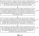
- a data transmission circuit comprising: a global data line; a local data line; a data bus node connectable to a data bus; a comparison module, configured to receive first data on the data bus node and second data on the global data line, and compare the first data with the second data to output a comparison result of whether a number of different bits between the first data and the second data exceeds a preset threshold, wherein the first data and the second data have a same preset bit width; a data conversion module electrically connected to the data bus node, the comparison module and the global data line, and configured to: invert the first data and transmit the inverted first data to the global data line in response to the comparison result indicating that the number of different bits exceeds the preset threshold, and transmit the first data to the global data line in response to the comparison result indicating that the number of different bits does not exceed the preset threshold; and a read-write conversion circuit electrically connected to the global data line and the local data line, and
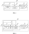
- a data transmission circuit 100 which includes a comparison module 10, a data conversion module 20, and a read-write conversion circuit 70.
- the comparison module 10 is configured to receive first data on a data bus 30 and second data on a global data line 40, and compare the first data with the second data to output a comparison result of whether a number of different bits between the first data and the second data exceeds a preset threshold, where the first data and the second data have a same preset bit width.
- the read-write conversion circuit 70 is electrically connected to the global data line 40, a local data line 81 and a complementary local data line 82, and is configured to: in a case that the comparison result indicates that the number of different bits exceeds the preset threshold, transmit data on the global data line 40 to the complementary local data line 82; and in a case that the comparison result indicates that the number of different bits does not exceed the preset threshold, transmit data on the global data line 40 to the local data line 81.
- the data bus 30 is intended to schematically illustrate a front-stage data line of the global data line 40 in the process of writing data into the semiconductor storage apparatus, and is not used as the limitation to the present disclosure.
- the read-write conversion circuit 70 is configured to: pull down the local data line 81 to the low level when the global data line 40 is at the high level in a case that the comparison result output by the comparison module 10 indicates that the number of different bits exceeds the preset threshold; and pull down the complementary local data line 82 to the low level when the global data line 40 is at the high level in a case that the comparison result indicates that the number of different bits does not exceed the preset threshold.
- the read-write conversion circuit 70 it is convenient for the read-write conversion circuit 70 to transmit the data on the global data line 40 to the complementary local data line 82 in a case that the comparison result indicates that the number of different bits exceeds the preset threshold, and transmit the data on the global data line 40 to the local data line 81 in a case that the comparison result indicates that the number of different bits does not exceed the preset threshold, so that the data on the data bus 30 can be accurately transmitted to the local data line 81 or the complementary local data line 82 and the number of inversions of the data during the data transmission can be reduced, so as to effectively reduce the power consumption during the data transmission through the data bus 30, the global data line 40 and the local data line 81, or through the data bus 30, the global data line 40 and the complementary local data line 82.
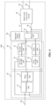
- the preset threshold is half of the preset bit width; and the comparison module 10 includes a comparison unit 11 and a state recognition unit 12.
- the comparison unit 11 is configured to compare the first data with the second data bit by bit and output comparison state data of respective bits.
- the state recognition unit 12 is electrically connected to the comparison unit 11 and is configured to perform statistics on the comparison state data of the respective bits and output the comparison result according to a statistical result.
- the number of inversions of the data is reduced under the premise that the accuracy of the data transmission is ensured, so as to effectively reduce the power consumption during the data transmission.
- the data conversion module 20 includes a first transmission unit 21, a first inverter unit 22, a second transmission unit 23, and a second inverter unit 24.
- the first transmission unit 21 is electrically connected to the data bus 30 and the global data line 40 and is electrically connected to an output terminal of the state recognition unit 12 through the first inverter unit 22, and is configured to transmit the first data to the global data line 40 in a case that the comparison result output by the comparison module 10 indicates that the number of different bits does not exceed the preset threshold.
- the read-write conversion circuit 70 includes a write enable module 71 and a write drive circuit 72.
- the write enable module 71 is configured to generate a write enable signal WrEn and an inverted write enable signal WrEn_ according to the data polarity identification signal pl and an initial write enable signal we.
- the write drive circuit 72 is configured to generate third data according to the write enable signal WrEn, the inverted write enable signal WrEn_ and the second data, and transmit the third data to the local data line 81 or the complementary local data line 82, to ensure the accuracy of the data transmission.
- the write enable module 71 includes a first inverter Inv1, a first NOR gate Nor1, a second inverter Inv2, and a second NOR gate Nor2.
- the first inverter Inv1 has an input terminal configured to be electrically connected to the initial write enable signal we, and an output terminal configured to output a first inverted write enable signal We1_.
- the first NOR gate Nor1 has input terminals configured to be electrically connected to the data polarity identification signal pl and the output terminal of the first inverter Inv1, and an output terminal configured to output the write enable signal WrEn.
- the second inverter Inv2 has an input terminal configured to be electrically connected to the data polarity identification signal pl, and an output terminal configured to output an inverted data polarity identification signal Pl_.
- the second NOR gate Nor2 has input terminals configured to be electrically connected to the output terminal of the second inverter Inv2 and the output terminal of the first inverter Inv1, and an output terminal configured to output the inverted write enable signal WrEn_.
- the write drive circuit 72 includes a first switch unit 721, a second switch unit 722, a third switch unit 723, a fourth switch unit 724, a fifth switch unit 725, and a sixth switch unit 726.
- the first switch unit 721 is configured to be electrically connected to the complementary local data line LIO_ and the global data line YIO according to the inverted write enable signal WrEn_.
- the second switch unit 722 has a control terminal configured to be electrically connected to the global data line YIO, a first terminal configured to be electrically connected to the local data line LIO, and a second terminal configured to be electrically connected to a first node a.
- the third switch unit 723 is configured to be electrically connected to the first node a and a ground according to the inverted write enable signal WrEn_.
- the fourth switch unit 724 is configured to be electrically connected to the local data line LIO and the global data line YIO according to the write enable signal WrEn.
- the fifth switch unit 725 has a control terminal configured to be electrically connected to the global data line YIO, a first terminal configured to be electrically connected to the complementary local data line LIO_, and a second terminal configured to be electrically connected to a second node b.
- the sixth switch unit 726 is configured to be electrically connected to the second node b and the ground according to the write enable signal WrEn.
- the power consumption in the process of writing the data into the local data line LIO or the complementary local data line LIO_ through the data bus Data bus and the global data line YIO is effectively reduced by reducing the number of inversions of the written data in the transmission process, and in particular, the inversions of the data on the global data line YIO are reduced.
- the data conversion module 20 inverts the second data provided by the global data line 40 and transmit the inverted second data to the data bus 30; and in a case that the comparison result output by the comparison module 10 indicates that the number of different bits does not exceed the preset threshold, the data conversion module 20 transmits the second data provided by the global data line 40 to the data bus 30, so as to effectively reduce the power consumption in the process of transmitting the read data to the data bus 30 through the global data line 40.
- the preset threshold e.g., half of the preset bit width
- the data conversion module 20 further includes a third transmission unit 25, a third inverter unit 26, a fourth transmission unit 27, and a fourth inverter unit 28.
- the third transmission unit 25 is electrically connected to the data bus 30 and the global data line 40 and is electrically connected to an output terminal of the comparison module 10 through the third inverter unit 26, and is configured to transmit the second data to the data bus 30 in a case that the comparison result output by the comparison module 10 indicates that the number of different bits does not exceed the preset threshold.
- the transmitted data generally includes a data string consisting of 0 and 1
- the number of inversions of the data is reduce to effectively reduce the power consumption during the transmission of the data through the data bus, the global data line and the local data line, or through the data bus, the global data line and the complementary local data line. Therefore, the energy consumption of the semiconductor storage apparatus is reduced in a case of ensuring that the density and number of the storage cells in the storage cell array are not reduced. Since the data transmitted by the local data line and the complementary local data line can be used as references to each other, the accuracy of data transmission to the rear-stage circuit is improved while ensuring the efficiency of the data transmission.
- An embodiment of the present disclosure provides a computer-readable storage medium, having a computer program stored thereon that, when executed by a processor, cause the processor to perform the data transmission method of any one of the embodiments of the present disclosure.
Landscapes
- Engineering & Computer Science (AREA)
- Theoretical Computer Science (AREA)
- Human Computer Interaction (AREA)
- Physics & Mathematics (AREA)
- General Engineering & Computer Science (AREA)
- General Physics & Mathematics (AREA)
- Microelectronics & Electronic Packaging (AREA)
- Computer Hardware Design (AREA)
- Dc Digital Transmission (AREA)
Claims (10)
- Datenübertragungsschaltung (100), umfassend:eine globale Datenleitung (40), eine lokale Datenleitung (81) und eine komplementäre lokale Datenleitung (82);einen Datenbusknoten, der an einen Datenbus (30) angeschlossen werden kann;
ein Vergleichsmodul (10), das so konfiguriert ist, dass es erste Daten auf dem Datenbusknoten undzweite Daten auf derglobalen Datenleitung (40) empfängt und die ersten Daten mit den zweiten Daten vergleicht, um ein Vergleichsergebnis auszugeben, ob eine Anzahl unterschiedlicher Bits zwischen den ersten Daten und den zweiten Daten einen voreingestellten Schwellenwert überschreitet, wobei die ersten Daten und die zweiten Daten eine gleiche voreingestellte Bitbreite haben;ein Datenbus-Puffermodul (50);
ein Datenumwandlungsmodul (20), das elektrisch mit dem Datenbusknoten, dem Vergleichsmodul (20) und, über das Datenbus-Puffermodul (50),mit der globalen Datenleitung (40) verbunden ist und das so konfiguriert ist, dass es: die ersten Daten invertiert und, über das Datenbus-Puffermodul (50),die invertierten ersten Daten an die globale Datenleitung (40) überträgt, wenn das Vergleichsergebnis anzeigt, dass die Anzahl der unterschiedlichen Bits den voreingestellten Schwellenwert überschreitet, und, über das Datenbus-Puffermodul (50),die ersten Daten an die globale Datenleitung (40) überträgt, wenn das Vergleichsergebnis anzeigt, dass die Anzahl der unterschiedlichen Bits den voreingestellten Schwellenwert nicht überschreitet; und
eine Lese-Schreib-Umwandlungsschaltung (70), die elektrisch mit der globalen Datenleitung (40),der lokalen Datenleitung (81) und derkomplementären lokalen Datenleitung (82) verbunden ist und so konfiguriert ist, dass sie: Daten auf der globalen Datenleitung (40) als Reaktion auf das Vergleichsergebnis, das anzeigt, dass die Anzahl unterschiedlicher Bits den voreingestellten Schwellenwert überschreitet, an die komplementäre lokale Datenleitung (82) überträgt, und Daten auf der globalen Datenleitung (40) als Reaktion auf das Vergleichsergebnis, das anzeigt, dass die Anzahl unterschiedlicher Bits den voreingestellten Schwellenwert nicht überschreitet, an die lokale Datenleitung (81) überträgt;
wobei der voreingestellte Schwellenwert die Hälfte der voreingestellten Bitbreite ist; und das Vergleichsmodul (10) umfasst ferner Folgendes:eine Vergleichseinheit (11), die so konfiguriert ist, dass sie die ersten Daten Bit für Bit mit den zweiten Daten vergleicht und Vergleichszustandsdaten der jeweiligen Bits ausgibt; undeine Zustandserkennungseinheit (12), die elektrisch mit der Vergleichseinheit (11) verbunden und so konfiguriert ist, dass sie eine Statistik über die Vergleichszustandsdaten der jeweiligen Bits durchführt und das Vergleichsergebnis entsprechend einem statistischen Ergebnis ausgibt;wobei das Datenumwandlungsmodul (20) über das Datenbus-Puffermodul (50) elektrisch mit der Lese-Schreib-Umwandlungsschaltung (70) verbunden ist; und das Datenbus-Puffermodul (50) ferner elektrisch mit der Zustandserkennungseinheit (12) verbunden und so konfiguriert ist, dass es ein Datenpolaritäts-Identifikationssignal entsprechend dem Vergleichsergebnis erzeugt;wobei das Datenbus-Puffermodul (50) eine Schreibeinheit (51) umfasst, die so konfiguriert ist, dass sie die ersten Daten an die globale Datenleitung (40) oder die invertierten ersten Daten an die globale Datenleitung (40) überträgt; undwobei die Lese-Schreib-Umwandlungsschaltung (70) Folgendes umfasst:ein Schreibfreigabemodul (71), das so konfiguriert ist, dass es ein Schreibfreigabesignal und ein invertiertes Schreibfreigabesignal entsprechend dem Datenpolaritäts-Identifikationssignal und einem anfänglichen Schreibfreigabesignal erzeugt; undeine Schreibtreiberschaltung (72), die so konfiguriert ist, dass sie dritte Daten gemäß dem Schreibfreigabesignal, dem invertierten Schreibfreigabesignal und den Daten auf der globalen Datenleitung erzeugt und die dritten Datenan die lokale Datenleitung (81) oder die komplementäre lokale Datenleitung (82) überträgt. - Datenübertragungsschaltung nach Anspruch 1, wobei die Lese-Schreib-Umwandlungsschaltung so konfiguriert ist, dass sie:als Reaktion auf das Vergleichsergebnis, das anzeigt, dass die Anzahl der unterschiedlichen Bits den voreingestellten Schwellenwert überschreitet, die lokale Datenleitung (81) auf einen niedrigen Pegel herunterzieht, wenn die globale Datenleitung (40) auf einem hohen Pegel ist; und,als Reaktion auf das Vergleichsergebnis, das anzeigt, dass die Anzahl der unterschiedlichen Bits den voreingestellten Schwellenwert nicht überschreitet, die komplementäre lokale Datenleitung (82) auf den niedrigen Pegel herunterzieht, wenn die globale Datenleitung (40) auf dem hohen Pegel ist.
- Datenübertragungsschaltung nach Anspruch 1, wobei das Datenumwandlungsmodul (20) Folgendes umfasst:eine erste Übertragungseinheit (21) und eine erste Invertereinheit (22), wobei die erste Übertragungseinheit (21) elektrisch mit dem Datenbusknoten und der Schreibeinheit (51) und elektrisch mit einem Ausgangsanschluss der Zustandserkennungseinheit (12) über die erste Invertereinheit (22) verbunden ist und wobei die erste Übertragungseinheit (21) und die Schreibeinheit (51) so konfiguriert sind, dass sie die ersten Daten als Reaktion auf das Vergleichsergebnis, das anzeigt, dass die Anzahl der unterschiedlichen Bits den voreingestellten Schwellenwert nicht überschreitet, an die globale Datenleitung (40) übertragen; undeine zweite Übertragungseinheit (23) und eine zweite Invertereinheit (24), wobei die zweite Übertragungseinheit (23) elektrisch mit der Schreibeinheit (51)und dem Ausgangsanschlussder Zustandserkennungseinheit (12) verbunden ist und elektrisch mit dem Datenbusknoten über die zweite Invertereinheit (24) verbunden ist und der zweite Inverter (24) so konfiguriert ist, dass er die ersten Daten invertiert, wobei die zweite Übertragungseinheit (23) und der Schreibtreiber (51) so konfiguriert sind, dasssie die invertierten ersten Daten in Reaktion auf das Vergleichsergebnis, das anzeigt, dass die Anzahl der unterschiedlichen Bits den voreingestellten Schwellenwert überschreitet, an die globale Datenleitung (40) übertragen.
- Datenübertragungsschaltung nach Anspruch 1, wobei das Schreibfreigabemodul (71) Folgendes umfasst:einen ersten Inverter (Inv1), der so konfiguriert ist, dass er das anfängliche Schreibfreigabesignal (we) empfängt und ein erstes invertiertes Schreibfreigabesignal (we1_) ausgibt;ein erstes NOR-Gate (Nor1), das so konfiguriert ist, dass es das Datenpolaritäts-Identifikationssignal (pl) und das erste invertierte Schreibfreigabesignal (We1_) empfängt, und das einen Ausgangsanschluss aufweist, der so konfiguriert ist, dass er das Schreibfreigabesignal (WrEn) ausgibt;einen zweiten Inverter (Inv2), der so konfiguriert ist, dass er das Datenpolaritäts-Identifikationssignal empfängt, und der einen Ausgangsanschluss aufweist, der so konfiguriert ist, dass er ein invertiertes Datenpolaritäts-Identifikationssignal (PI_) ausgibt; undein zweites NOR-Gate (Nor2), das Eingangsanschlüsse aufweist, die so konfiguriert sind, dass sie mit dem Ausgangsanschluss des zweiten Inverters (Inv2) und dem Ausgangsanschluss des ersten Inverters (Inv1) elektrisch verbunden sind, und einen Ausgangsanschluss aufweist, der so konfiguriert ist, dass er das invertierte Schreibfreigabesignal ausgibt.
- Datenübertragungsschaltung nach Anspruch 4, wobei das Schreibtreibermodul (72) Folgendes umfasst:eine erste Schalteinheit (721), die so konfiguriert ist, dass sie die komplementäre lokale Datenleitung (82, LIO_) entsprechend dem invertierten Schreibfreigabesignal mit der globalen Datenleitung (40, YIO) verbindet;eine zweite Schalteinheit (722), die einen Steueranschluss, der so konfiguriert ist, dass er elektrisch mit der globalen Datenleitung (40, YIO) verbunden ist, einen ersten Anschluss, der so konfiguriert ist, dass er elektrisch mit der lokalen Datenleitung (81, LIO) verbunden ist, und einen zweiten Anschluss aufweist, der mit einem ersten Knoten (a) verbunden ist;eine dritte Schalteinheit (723), die so konfiguriert ist, dass sie den ersten Knoten (a) entsprechend dem invertierten Schreibfreigabesignal mit einer Masse verbindet;eine vierte Schalteinheit (724), die so konfiguriert ist, dass sie die lokale Datenleitung (81 LIO) entsprechend dem Schreibfreigabesignal mit der globalen Datenleitung (40, YIO) verbindet;eine fünfte Schalteinheit (725), die einen Steueranschluss, der so konfiguriert ist, dass er elektrisch mit der globalen Datenleitung (40) verbunden ist, einen ersten Anschluss, der so konfiguriert ist, dass er elektrisch mit der komplementären lokalen Datenleitung (82) verbunden ist, und einen zweiten Anschluss aufweist, der mit einem zweiten Knoten verbunden ist; undeine sechste Schalteinheit (726), die so konfiguriert ist, dass sie den zweiten Knoten entsprechend dem Schreibfreigabesignal mit der Masse verbindet.
- Datenübertragungsschaltung nach einem der Ansprüche 1 bis 5, wobei das Datenumwandlungsmodul (20) ferner so konfiguriert ist, dass es: die zweiten Daten invertiert und die invertierten zweiten Daten an den Datenbus (30) überträgt, wenn das Vergleichsergebnis anzeigt, dass die Anzahl der unterschiedlichen Bits den voreingestellten Schwellenwert überschreitet, und die zweiten Daten an den Datenbus (30) überträgt, wenn das Vergleichsergebnis anzeigt, dass die Anzahl der unterschiedlichen Bits den voreingestellten Schwellenwert nicht überschreitet.
- Datenübertragungsschaltung nach Anspruch 6 und 3, wobei das Datenumwandlungsmodul (20) ferner Folgendes umfasst:eine dritte Übertragungseinheit (25) und eine dritte Invertereinheit (26), wobei die dritte Übertragungseinheit (25) elektrisch mit dem Datenbus-1-Knoten und dem Datenbus-Puffermodul (50) verbunden ist und elektrisch mit einem Ausgangsanschluss des Vergleichsmoduls (10) über die dritte Invertereinheit (26) verbunden ist und so konfiguriert ist, dass sie die zweiten Daten als Reaktion auf das Vergleichsergebnis, das anzeigt, dass die Anzahl der unterschiedlichen Bits den voreingestellten Schwellenwert nicht überschreitet, an den Datenbus-Knoten überträgt; undeine vierte Übertragungseinheit (27) und eine vierte Invertereinheit (28), wobei die vierte Übertragungseinheit (27) elektrisch mit dem Datenbusknoten und dem Ausgangsanschluss des Vergleichsmoduls (10) verbunden ist und elektrisch mit dem Datenbus-Puffermodul (50) über die vierte Invertereinheit (28) verbunden ist und wobei die vierte Invertereinheit (28) so konfiguriert ist, dass sie die zweiten Daten invertiert, und die vierte Übertragungseinheit (27) so konfiguriert ist, dass sie die invertierten zweiten Daten als Reaktion auf das Vergleichsergebnis, das anzeigt, dass die Anzahl der Bits den voreingestellten Schwellenwert überschreitet, an den Datenbusknoten überträgt.
- Datenübertragungsschaltung nach Anspruch 7, wobei das Datenbus-Puffermodul (50) ferner Folgendes umfasst:
eine Leseeinheit (52), die so konfiguriert ist, dass sie die zweiten Daten an die dritte Übertragungseinheit (25) oder an die vierte Invertereinheit (28) überträgt. - Datenübertragungsschaltung nach einem der Ansprüche 1 bis 5, die ferner Folgendes umfasst:
eine Vorladeschaltung, die sowohl mit der lokalen Datenleitung (81) als auch mit der komplementären lokalen Datenleitung (82) elektrisch verbunden und so konfiguriert ist, dass sie sowohl die lokale Datenleitung (81) als auch die komplementäre lokale Datenleitung (82) auf einen hohen Pegel vorlädt, bevor die globale Datenleitung (40) die Daten an die lokale Datenleitung (81) oder die komplementäre lokale Datenleitung (82) überträgt. - Speichervorrichtung (200), umfassend:
Datenübertragungsschaltung (100) nach einem der Ansprüche 1 bis 9, die so konfiguriert ist, dass sie Daten während eines Lesevorgangs oder eines Schreibvorgangs speichert und überträgt.
Applications Claiming Priority (2)
| Application Number | Priority Date | Filing Date | Title |
|---|---|---|---|
| CN202110328177.4A CN115129234B (zh) | 2021-03-26 | 2021-03-26 | 数据传输电路、方法及存储装置 |
| PCT/CN2021/108597 WO2022198865A1 (zh) | 2021-03-26 | 2021-07-27 | 数据传输电路、方法及存储装置 |
Publications (3)
| Publication Number | Publication Date |
|---|---|
| EP4180934A1 EP4180934A1 (de) | 2023-05-17 |
| EP4180934A4 EP4180934A4 (de) | 2024-03-06 |
| EP4180934B1 true EP4180934B1 (de) | 2025-04-09 |
Family
ID=83364962
Family Applications (1)
| Application Number | Title | Priority Date | Filing Date |
|---|---|---|---|
| EP21932477.9A Active EP4180934B1 (de) | 2021-03-26 | 2021-07-27 | Datenübertragungsschaltung und -verfahren sowie speichervorrichtung |
Country Status (2)
| Country | Link |
|---|---|
| US (1) | US11862286B2 (de) |
| EP (1) | EP4180934B1 (de) |
Families Citing this family (5)
| Publication number | Priority date | Publication date | Assignee | Title |
|---|---|---|---|---|
| CN115206360B (zh) * | 2021-04-13 | 2026-03-27 | 长鑫存储技术有限公司 | 数据传输电路、方法及存储装置 |
| US11901028B2 (en) | 2021-04-13 | 2024-02-13 | Changxin Memory Technologies, Inc. | Data transmission circuit, data transmission method, and storage apparatus |
| CN115206362A (zh) | 2021-04-13 | 2022-10-18 | 长鑫存储技术有限公司 | 数据传输电路、方法及存储装置 |
| US11810637B2 (en) * | 2021-04-13 | 2023-11-07 | Changxin Memory Technologies, Inc. | Data transmission circuit, data transmission method, and storage apparatus with read-write conversion circuit |
| CN119446217A (zh) * | 2023-08-03 | 2025-02-14 | 长鑫科技集团股份有限公司 | 读写转换电路、写驱动电路与存储器 |
Family Cites Families (14)
| Publication number | Priority date | Publication date | Assignee | Title |
|---|---|---|---|---|
| KR0172368B1 (ko) * | 1995-09-29 | 1999-03-30 | 김광호 | 저전력 반도체 메모리 장치 |
| US6898648B2 (en) * | 2002-02-21 | 2005-05-24 | Micron Technology, Inc. | Memory bus polarity indicator system and method for reducing the affects of simultaneous switching outputs (SSO) on memory bus timing |
| KR100643498B1 (ko) * | 2005-11-21 | 2006-11-10 | 삼성전자주식회사 | 반도체 메모리에서의 데이터 버스 반전 회로 및 데이터버스 반전 방법 |
| US7501963B1 (en) * | 2007-10-17 | 2009-03-10 | Micron Technology, Inc. | Balanced data bus inversion |
| JP4399015B2 (ja) * | 2008-04-30 | 2010-01-13 | 株式会社東芝 | データ変換装置、情報記録装置、誤り検出装置、データ変換方法および誤り検出方法 |
| JP2010081577A (ja) * | 2008-08-26 | 2010-04-08 | Elpida Memory Inc | 半導体装置およびデータ伝送システム |
| KR20130048394A (ko) * | 2011-11-02 | 2013-05-10 | 삼성전자주식회사 | 반도체 메모리 장치 및 이를 포함하는 메모리 시스템 |
| KR20150038792A (ko) * | 2013-09-30 | 2015-04-09 | 에스케이하이닉스 주식회사 | 반도체 메모리 장치 및 이의 데이터 입출력 방법 |
| KR20150051673A (ko) * | 2013-11-05 | 2015-05-13 | 에스케이하이닉스 주식회사 | 메모리 장치 및 이를 포함하는 시스템 |
| KR20160094154A (ko) * | 2015-01-30 | 2016-08-09 | 에스케이하이닉스 주식회사 | 데이터 전송 회로 |
| JP6765331B2 (ja) * | 2017-03-24 | 2020-10-07 | キオクシア株式会社 | メモリシステム |
| US20210098057A1 (en) * | 2019-09-26 | 2021-04-01 | Qualcomm Incorporated | Sram low-power write driver |
| CN210667806U (zh) * | 2019-10-25 | 2020-06-02 | 长鑫存储技术(上海)有限公司 | 读操作电路和半导体存储器 |
| CN115206360B (zh) * | 2021-04-13 | 2026-03-27 | 长鑫存储技术有限公司 | 数据传输电路、方法及存储装置 |
-
2021
- 2021-07-27 EP EP21932477.9A patent/EP4180934B1/de active Active
-
2022
- 2022-01-27 US US17/649,068 patent/US11862286B2/en active Active
Also Published As
| Publication number | Publication date |
|---|---|
| EP4180934A4 (de) | 2024-03-06 |
| EP4180934A1 (de) | 2023-05-17 |
| US20220310139A1 (en) | 2022-09-29 |
| US11862286B2 (en) | 2024-01-02 |
Similar Documents
| Publication | Publication Date | Title |
|---|---|---|
| US11862286B2 (en) | Data transmission circuit and method, and storage apparatus | |
| US9886378B2 (en) | Nonvolatile memory system using control signals to transmit varied signals via data pins | |
| CN110058794B (zh) | 用于动态执行垃圾回收数据储存装置与操作方法 | |
| US20170337951A1 (en) | Apparatuses and methods for performing intra-module databus inversion operations | |
| US8934298B2 (en) | Nonvolatile memory device and related programming method | |
| US11934325B2 (en) | Memory device interface communicating with set of data bursts corresponding to memory dies via dedicated portions for command processing | |
| EP4198704B1 (de) | Datenübertragungsschaltung sowie speichervorrichtung | |
| US11626147B2 (en) | Transmission circuit, transmission method, storage apparatus, and storage medium | |
| CN115129234B (zh) | 数据传输电路、方法及存储装置 | |
| US11810637B2 (en) | Data transmission circuit, data transmission method, and storage apparatus with read-write conversion circuit | |
| CN115129231B (zh) | 传输电路、方法、存储装置及存储介质 | |
| CN115129235B (zh) | 数据传输电路、方法及存储装置 | |
| US11901028B2 (en) | Data transmission circuit, data transmission method, and storage apparatus | |
| US7437499B2 (en) | Dividing a flash memory operation into phases | |
| US11790960B2 (en) | Data transmission circuit, method and storage device | |
| CN115206361B (zh) | 数据传输电路、方法及存储装置 | |
| US12131797B2 (en) | Data transmission circuit, data transmission method and memory device | |
| CN108052464A (zh) | 用于分散与降低非易失性储存装置峰值电流与功耗的方法 | |
| KR102838329B1 (ko) | 데이터 전송 회로, 데이터 전송 방법 및 메모리 | |
| US20170229162A1 (en) | Nonvolatile ram | |
| WO2022217844A1 (zh) | 数据传输电路、方法及存储装置 | |
| KR100489420B1 (ko) | 터너리 정보를 저장할 수 있는 내용 주소화 메모리 장치 | |
| US20150138899A1 (en) | Data storage device and operating method thereof | |
| CN118113227A (zh) | 固态硬盘进退低功耗模式的优化方法、装置和计算机设备 | |
| CN111930220A (zh) | 用于分散与降低非易失性储存装置峰值电流与功耗的方法 |
Legal Events
| Date | Code | Title | Description |
|---|---|---|---|
| STAA | Information on the status of an ep patent application or granted ep patent |
Free format text: STATUS: THE INTERNATIONAL PUBLICATION HAS BEEN MADE |
|
| PUAI | Public reference made under article 153(3) epc to a published international application that has entered the european phase |
Free format text: ORIGINAL CODE: 0009012 |
|
| STAA | Information on the status of an ep patent application or granted ep patent |
Free format text: STATUS: REQUEST FOR EXAMINATION WAS MADE |
|
| 17P | Request for examination filed |
Effective date: 20230208 |
|
| AK | Designated contracting states |
Kind code of ref document: A1 Designated state(s): AL AT BE BG CH CY CZ DE DK EE ES FI FR GB GR HR HU IE IS IT LI LT LU LV MC MK MT NL NO PL PT RO RS SE SI SK SM TR |
|
| A4 | Supplementary search report drawn up and despatched |
Effective date: 20240207 |
|
| RIC1 | Information provided on ipc code assigned before grant |
Ipc: G11C 7/10 20060101ALI20240201BHEP Ipc: G06F 3/06 20060101AFI20240201BHEP |
|
| DAV | Request for validation of the european patent (deleted) | ||
| DAX | Request for extension of the european patent (deleted) | ||
| GRAP | Despatch of communication of intention to grant a patent |
Free format text: ORIGINAL CODE: EPIDOSNIGR1 |
|
| STAA | Information on the status of an ep patent application or granted ep patent |
Free format text: STATUS: GRANT OF PATENT IS INTENDED |
|
| INTG | Intention to grant announced |
Effective date: 20241104 |
|
| P01 | Opt-out of the competence of the unified patent court (upc) registered |
Free format text: CASE NUMBER: APP_66602/2024 Effective date: 20241217 |
|
| GRAS | Grant fee paid |
Free format text: ORIGINAL CODE: EPIDOSNIGR3 |
|
| GRAA | (expected) grant |
Free format text: ORIGINAL CODE: 0009210 |
|
| STAA | Information on the status of an ep patent application or granted ep patent |
Free format text: STATUS: THE PATENT HAS BEEN GRANTED |
|
| AK | Designated contracting states |
Kind code of ref document: B1 Designated state(s): AL AT BE BG CH CY CZ DE DK EE ES FI FR GB GR HR HU IE IS IT LI LT LU LV MC MK MT NL NO PL PT RO RS SE SI SK SM TR |
|
| REG | Reference to a national code |
Ref country code: GB Ref legal event code: FG4D |
|
| REG | Reference to a national code |
Ref country code: CH Ref legal event code: EP |
|
| REG | Reference to a national code |
Ref country code: DE Ref legal event code: R096 Ref document number: 602021029085 Country of ref document: DE |
|
| REG | Reference to a national code |
Ref country code: IE Ref legal event code: FG4D |
|
| REG | Reference to a national code |
Ref country code: NL Ref legal event code: MP Effective date: 20250409 |
|
| PG25 | Lapsed in a contracting state [announced via postgrant information from national office to epo] |
Ref country code: NL Free format text: LAPSE BECAUSE OF FAILURE TO SUBMIT A TRANSLATION OF THE DESCRIPTION OR TO PAY THE FEE WITHIN THE PRESCRIBED TIME-LIMIT Effective date: 20250409 |
|
| REG | Reference to a national code |
Ref country code: AT Ref legal event code: MK05 Ref document number: 1784126 Country of ref document: AT Kind code of ref document: T Effective date: 20250409 |
|
| PG25 | Lapsed in a contracting state [announced via postgrant information from national office to epo] |
Ref country code: FI Free format text: LAPSE BECAUSE OF FAILURE TO SUBMIT A TRANSLATION OF THE DESCRIPTION OR TO PAY THE FEE WITHIN THE PRESCRIBED TIME-LIMIT Effective date: 20250409 Ref country code: ES Free format text: LAPSE BECAUSE OF FAILURE TO SUBMIT A TRANSLATION OF THE DESCRIPTION OR TO PAY THE FEE WITHIN THE PRESCRIBED TIME-LIMIT Effective date: 20250409 Ref country code: PT Free format text: LAPSE BECAUSE OF FAILURE TO SUBMIT A TRANSLATION OF THE DESCRIPTION OR TO PAY THE FEE WITHIN THE PRESCRIBED TIME-LIMIT Effective date: 20250811 |
|
| PGFP | Annual fee paid to national office [announced via postgrant information from national office to epo] |
Ref country code: DE Payment date: 20250722 Year of fee payment: 5 |
|
| REG | Reference to a national code |
Ref country code: LT Ref legal event code: MG9D |
|
| PG25 | Lapsed in a contracting state [announced via postgrant information from national office to epo] |
Ref country code: GR Free format text: LAPSE BECAUSE OF FAILURE TO SUBMIT A TRANSLATION OF THE DESCRIPTION OR TO PAY THE FEE WITHIN THE PRESCRIBED TIME-LIMIT Effective date: 20250710 Ref country code: NO Free format text: LAPSE BECAUSE OF FAILURE TO SUBMIT A TRANSLATION OF THE DESCRIPTION OR TO PAY THE FEE WITHIN THE PRESCRIBED TIME-LIMIT Effective date: 20250709 |
|
| PG25 | Lapsed in a contracting state [announced via postgrant information from national office to epo] |
Ref country code: PL Free format text: LAPSE BECAUSE OF FAILURE TO SUBMIT A TRANSLATION OF THE DESCRIPTION OR TO PAY THE FEE WITHIN THE PRESCRIBED TIME-LIMIT Effective date: 20250409 |
|
| PG25 | Lapsed in a contracting state [announced via postgrant information from national office to epo] |
Ref country code: BG Free format text: LAPSE BECAUSE OF FAILURE TO SUBMIT A TRANSLATION OF THE DESCRIPTION OR TO PAY THE FEE WITHIN THE PRESCRIBED TIME-LIMIT Effective date: 20250409 |
|
| PGFP | Annual fee paid to national office [announced via postgrant information from national office to epo] |
Ref country code: GB Payment date: 20250724 Year of fee payment: 5 |
|
| PG25 | Lapsed in a contracting state [announced via postgrant information from national office to epo] |
Ref country code: HR Free format text: LAPSE BECAUSE OF FAILURE TO SUBMIT A TRANSLATION OF THE DESCRIPTION OR TO PAY THE FEE WITHIN THE PRESCRIBED TIME-LIMIT Effective date: 20250409 |
|
| PG25 | Lapsed in a contracting state [announced via postgrant information from national office to epo] |
Ref country code: AT Free format text: LAPSE BECAUSE OF FAILURE TO SUBMIT A TRANSLATION OF THE DESCRIPTION OR TO PAY THE FEE WITHIN THE PRESCRIBED TIME-LIMIT Effective date: 20250409 |
|
| PG25 | Lapsed in a contracting state [announced via postgrant information from national office to epo] |
Ref country code: RS Free format text: LAPSE BECAUSE OF FAILURE TO SUBMIT A TRANSLATION OF THE DESCRIPTION OR TO PAY THE FEE WITHIN THE PRESCRIBED TIME-LIMIT Effective date: 20250709 |
|
| PG25 | Lapsed in a contracting state [announced via postgrant information from national office to epo] |
Ref country code: IS Free format text: LAPSE BECAUSE OF FAILURE TO SUBMIT A TRANSLATION OF THE DESCRIPTION OR TO PAY THE FEE WITHIN THE PRESCRIBED TIME-LIMIT Effective date: 20250809 |
|
| PG25 | Lapsed in a contracting state [announced via postgrant information from national office to epo] |
Ref country code: LV Free format text: LAPSE BECAUSE OF FAILURE TO SUBMIT A TRANSLATION OF THE DESCRIPTION OR TO PAY THE FEE WITHIN THE PRESCRIBED TIME-LIMIT Effective date: 20250409 |
|
| REG | Reference to a national code |
Ref country code: DE Ref legal event code: R097 Ref document number: 602021029085 Country of ref document: DE |
|
| PG25 | Lapsed in a contracting state [announced via postgrant information from national office to epo] |
Ref country code: DK Free format text: LAPSE BECAUSE OF FAILURE TO SUBMIT A TRANSLATION OF THE DESCRIPTION OR TO PAY THE FEE WITHIN THE PRESCRIBED TIME-LIMIT Effective date: 20250409 Ref country code: SM Free format text: LAPSE BECAUSE OF FAILURE TO SUBMIT A TRANSLATION OF THE DESCRIPTION OR TO PAY THE FEE WITHIN THE PRESCRIBED TIME-LIMIT Effective date: 20250409 |
|
| PG25 | Lapsed in a contracting state [announced via postgrant information from national office to epo] |
Ref country code: CZ Free format text: LAPSE BECAUSE OF FAILURE TO SUBMIT A TRANSLATION OF THE DESCRIPTION OR TO PAY THE FEE WITHIN THE PRESCRIBED TIME-LIMIT Effective date: 20250409 |
|
| PG25 | Lapsed in a contracting state [announced via postgrant information from national office to epo] |
Ref country code: EE Free format text: LAPSE BECAUSE OF FAILURE TO SUBMIT A TRANSLATION OF THE DESCRIPTION OR TO PAY THE FEE WITHIN THE PRESCRIBED TIME-LIMIT Effective date: 20250409 |
|
| PG25 | Lapsed in a contracting state [announced via postgrant information from national office to epo] |
Ref country code: SK Free format text: LAPSE BECAUSE OF FAILURE TO SUBMIT A TRANSLATION OF THE DESCRIPTION OR TO PAY THE FEE WITHIN THE PRESCRIBED TIME-LIMIT Effective date: 20250409 |
|
| PG25 | Lapsed in a contracting state [announced via postgrant information from national office to epo] |
Ref country code: IT Free format text: LAPSE BECAUSE OF FAILURE TO SUBMIT A TRANSLATION OF THE DESCRIPTION OR TO PAY THE FEE WITHIN THE PRESCRIBED TIME-LIMIT Effective date: 20250409 |
|
| PLBE | No opposition filed within time limit |
Free format text: ORIGINAL CODE: 0009261 |
|
| STAA | Information on the status of an ep patent application or granted ep patent |
Free format text: STATUS: NO OPPOSITION FILED WITHIN TIME LIMIT |
|
| REG | Reference to a national code |
Ref country code: CH Ref legal event code: L10 Free format text: ST27 STATUS EVENT CODE: U-0-0-L10-L00 (AS PROVIDED BY THE NATIONAL OFFICE) Effective date: 20260218 |
|
| REG | Reference to a national code |
Ref country code: CH Ref legal event code: H13 Free format text: ST27 STATUS EVENT CODE: U-0-0-H10-H13 (AS PROVIDED BY THE NATIONAL OFFICE) Effective date: 20260224 |
|
| PG25 | Lapsed in a contracting state [announced via postgrant information from national office to epo] |
Ref country code: RO Free format text: LAPSE BECAUSE OF FAILURE TO SUBMIT A TRANSLATION OF THE DESCRIPTION OR TO PAY THE FEE WITHIN THE PRESCRIBED TIME-LIMIT Effective date: 20250409 |
|
| PG25 | Lapsed in a contracting state [announced via postgrant information from national office to epo] |
Ref country code: LU Free format text: LAPSE BECAUSE OF NON-PAYMENT OF DUE FEES Effective date: 20250727 |
|
| 26N | No opposition filed |
Effective date: 20260112 |
|
| REG | Reference to a national code |
Ref country code: BE Ref legal event code: MM Effective date: 20250731 |
|
| PG25 | Lapsed in a contracting state [announced via postgrant information from national office to epo] |
Ref country code: BE Free format text: LAPSE BECAUSE OF NON-PAYMENT OF DUE FEES Effective date: 20250731 |
|
| PG25 | Lapsed in a contracting state [announced via postgrant information from national office to epo] |
Ref country code: FR Free format text: LAPSE BECAUSE OF NON-PAYMENT OF DUE FEES Effective date: 20250731 |
|
| PG25 | Lapsed in a contracting state [announced via postgrant information from national office to epo] |
Ref country code: CH Free format text: LAPSE BECAUSE OF NON-PAYMENT OF DUE FEES Effective date: 20250731 |