EP4178325A1 - Circuit board assembly and electronic device - Google Patents
Circuit board assembly and electronic device Download PDFInfo
- Publication number
- EP4178325A1 EP4178325A1 EP22826802.5A EP22826802A EP4178325A1 EP 4178325 A1 EP4178325 A1 EP 4178325A1 EP 22826802 A EP22826802 A EP 22826802A EP 4178325 A1 EP4178325 A1 EP 4178325A1
- Authority
- EP
- European Patent Office
- Prior art keywords
- circuit board
- concave surface
- wall
- frame plate
- board assembly
- Prior art date
- Legal status (The legal status is an assumption and is not a legal conclusion. Google has not performed a legal analysis and makes no representation as to the accuracy of the status listed.)
- Granted
Links
Images




Classifications
-
- H—ELECTRICITY
- H05—ELECTRIC TECHNIQUES NOT OTHERWISE PROVIDED FOR
- H05K—PRINTED CIRCUITS; CASINGS OR CONSTRUCTIONAL DETAILS OF ELECTRIC APPARATUS; MANUFACTURE OF ASSEMBLAGES OF ELECTRICAL COMPONENTS
- H05K1/00—Printed circuits
- H05K1/02—Details
- H05K1/14—Structural association of two or more printed circuits
- H05K1/144—Stacked arrangements of planar printed circuit boards
-
- H—ELECTRICITY
- H05—ELECTRIC TECHNIQUES NOT OTHERWISE PROVIDED FOR
- H05K—PRINTED CIRCUITS; CASINGS OR CONSTRUCTIONAL DETAILS OF ELECTRIC APPARATUS; MANUFACTURE OF ASSEMBLAGES OF ELECTRICAL COMPONENTS
- H05K1/00—Printed circuits
- H05K1/02—Details
- H05K1/11—Printed elements for providing electric connections to or between printed circuits
- H05K1/111—Pads for surface mounting, e.g. lay-out
- H05K1/112—Pads for surface mounting, e.g. lay-out directly combined with via connections
- H05K1/113—Via provided in pad; Pad over filled via
-
- H—ELECTRICITY
- H05—ELECTRIC TECHNIQUES NOT OTHERWISE PROVIDED FOR
- H05K—PRINTED CIRCUITS; CASINGS OR CONSTRUCTIONAL DETAILS OF ELECTRIC APPARATUS; MANUFACTURE OF ASSEMBLAGES OF ELECTRICAL COMPONENTS
- H05K1/00—Printed circuits
- H05K1/02—Details
- H05K1/14—Structural association of two or more printed circuits
- H05K1/145—Arrangements wherein electric components are disposed between and simultaneously connected to two planar printed circuit boards, e.g. Cordwood modules
-
- H—ELECTRICITY
- H05—ELECTRIC TECHNIQUES NOT OTHERWISE PROVIDED FOR
- H05K—PRINTED CIRCUITS; CASINGS OR CONSTRUCTIONAL DETAILS OF ELECTRIC APPARATUS; MANUFACTURE OF ASSEMBLAGES OF ELECTRICAL COMPONENTS
- H05K3/00—Apparatus or processes for manufacturing printed circuits
- H05K3/0011—Working of insulating substrates or insulating layers
- H05K3/0044—Mechanical working of the substrate, e.g. drilling or punching
-
- H—ELECTRICITY
- H05—ELECTRIC TECHNIQUES NOT OTHERWISE PROVIDED FOR
- H05K—PRINTED CIRCUITS; CASINGS OR CONSTRUCTIONAL DETAILS OF ELECTRIC APPARATUS; MANUFACTURE OF ASSEMBLAGES OF ELECTRICAL COMPONENTS
- H05K3/00—Apparatus or processes for manufacturing printed circuits
- H05K3/0011—Working of insulating substrates or insulating layers
- H05K3/0044—Mechanical working of the substrate, e.g. drilling or punching
- H05K3/0047—Drilling of holes
-
- H—ELECTRICITY
- H05—ELECTRIC TECHNIQUES NOT OTHERWISE PROVIDED FOR
- H05K—PRINTED CIRCUITS; CASINGS OR CONSTRUCTIONAL DETAILS OF ELECTRIC APPARATUS; MANUFACTURE OF ASSEMBLAGES OF ELECTRICAL COMPONENTS
- H05K3/00—Apparatus or processes for manufacturing printed circuits
- H05K3/0094—Filling or covering plated through-holes or blind plated vias, e.g. for masking or for mechanical reinforcement
-
- H—ELECTRICITY
- H05—ELECTRIC TECHNIQUES NOT OTHERWISE PROVIDED FOR
- H05K—PRINTED CIRCUITS; CASINGS OR CONSTRUCTIONAL DETAILS OF ELECTRIC APPARATUS; MANUFACTURE OF ASSEMBLAGES OF ELECTRICAL COMPONENTS
- H05K3/00—Apparatus or processes for manufacturing printed circuits
- H05K3/36—Assembling printed circuits with other printed circuits
- H05K3/368—Assembling printed circuits with other printed circuits parallel to each other
-
- H—ELECTRICITY
- H05—ELECTRIC TECHNIQUES NOT OTHERWISE PROVIDED FOR
- H05K—PRINTED CIRCUITS; CASINGS OR CONSTRUCTIONAL DETAILS OF ELECTRIC APPARATUS; MANUFACTURE OF ASSEMBLAGES OF ELECTRICAL COMPONENTS
- H05K3/00—Apparatus or processes for manufacturing printed circuits
- H05K3/40—Forming printed elements for providing electric connections to or between printed circuits
- H05K3/42—Plated through-holes or plated via connections
-
- H—ELECTRICITY
- H05—ELECTRIC TECHNIQUES NOT OTHERWISE PROVIDED FOR
- H05K—PRINTED CIRCUITS; CASINGS OR CONSTRUCTIONAL DETAILS OF ELECTRIC APPARATUS; MANUFACTURE OF ASSEMBLAGES OF ELECTRICAL COMPONENTS
- H05K1/00—Printed circuits
- H05K1/02—Details
- H05K1/14—Structural association of two or more printed circuits
- H05K1/141—One or more single auxiliary printed circuits mounted on a main printed circuit, e.g. modules, adapters
-
- H—ELECTRICITY
- H05—ELECTRIC TECHNIQUES NOT OTHERWISE PROVIDED FOR
- H05K—PRINTED CIRCUITS; CASINGS OR CONSTRUCTIONAL DETAILS OF ELECTRIC APPARATUS; MANUFACTURE OF ASSEMBLAGES OF ELECTRICAL COMPONENTS
- H05K2201/00—Indexing scheme relating to printed circuits covered by H05K1/00
- H05K2201/04—Assemblies of printed circuits
- H05K2201/042—Stacked spaced PCBs; Planar parts of folded flexible circuits having mounted components in between or spaced from each other
-
- H—ELECTRICITY
- H05—ELECTRIC TECHNIQUES NOT OTHERWISE PROVIDED FOR
- H05K—PRINTED CIRCUITS; CASINGS OR CONSTRUCTIONAL DETAILS OF ELECTRIC APPARATUS; MANUFACTURE OF ASSEMBLAGES OF ELECTRICAL COMPONENTS
- H05K2201/00—Indexing scheme relating to printed circuits covered by H05K1/00
- H05K2201/09—Shape and layout
- H05K2201/09145—Edge details
- H05K2201/09181—Notches in edge pads
-
- H—ELECTRICITY
- H05—ELECTRIC TECHNIQUES NOT OTHERWISE PROVIDED FOR
- H05K—PRINTED CIRCUITS; CASINGS OR CONSTRUCTIONAL DETAILS OF ELECTRIC APPARATUS; MANUFACTURE OF ASSEMBLAGES OF ELECTRICAL COMPONENTS
- H05K2201/00—Indexing scheme relating to printed circuits covered by H05K1/00
- H05K2201/10—Details of components or other objects attached to or integrated in a printed circuit board
- H05K2201/10227—Other objects, e.g. metallic pieces
- H05K2201/10378—Interposers
-
- H—ELECTRICITY
- H05—ELECTRIC TECHNIQUES NOT OTHERWISE PROVIDED FOR
- H05K—PRINTED CIRCUITS; CASINGS OR CONSTRUCTIONAL DETAILS OF ELECTRIC APPARATUS; MANUFACTURE OF ASSEMBLAGES OF ELECTRICAL COMPONENTS
- H05K2201/00—Indexing scheme relating to printed circuits covered by H05K1/00
- H05K2201/20—Details of printed circuits not provided for in H05K2201/01 - H05K2201/10
- H05K2201/2018—Presence of a frame in a printed circuit or printed circuit assembly
-
- Y—GENERAL TAGGING OF NEW TECHNOLOGICAL DEVELOPMENTS; GENERAL TAGGING OF CROSS-SECTIONAL TECHNOLOGIES SPANNING OVER SEVERAL SECTIONS OF THE IPC; TECHNICAL SUBJECTS COVERED BY FORMER USPC CROSS-REFERENCE ART COLLECTIONS [XRACs] AND DIGESTS
- Y02—TECHNOLOGIES OR APPLICATIONS FOR MITIGATION OR ADAPTATION AGAINST CLIMATE CHANGE
- Y02E—REDUCTION OF GREENHOUSE GAS [GHG] EMISSIONS, RELATED TO ENERGY GENERATION, TRANSMISSION OR DISTRIBUTION
- Y02E60/00—Enabling technologies; Technologies with a potential or indirect contribution to GHG emissions mitigation
- Y02E60/10—Energy storage using batteries
Definitions
- Embodiments of this application relate to the field of terminal technologies, and in particular, to a circuit board assembly and an electronic device.
- a plurality of circuit boards are usually stacked to provide a larger arrangement space for a battery and other functional modules in the electronic devices.
- electronic components may be scattered on the circuit boards. In this way, all the electronic components can be arranged without increasing areas of the circuit boards that bear the electronic components.
- circuit board assembly In the manner of stacking a plurality of circuit boards, two adjacent circuit boards are connected by using a frame plate.
- the frame plate and the circuit boards are assembled by soldering to form a circuit board assembly.
- Different circuit boards may be electrically connected to each other by using a frame plate to implement data information exchange. Because a circuit board and a frame plate are two mechanical parts designed separately, the circuit board and the frame plate are easily separated at a connection joint in a scenario with an uneven force such as a drop or a collision of an electronic device, causing a communication failure or malfunction of a circuit board assembly.
- Embodiments of this application provide a circuit board assembly and an electronic device, which can increase a connection force between a circuit board and a frame plate, and effectively reduce a possibility of separation between the circuit board and the frame plate.
- a first aspect of this application provides a circuit board assembly.
- the circuit board assembly is used in an electronic device.
- the circuit board assembly includes at least a frame plate and circuit boards.
- the frame plate includes a frame body, first soldering portions, and second soldering portions.
- the frame body has a middle accommodating hole, an inner wall facing the middle accommodating hole, and an outer wall facing away from the middle accommodating hole.
- the first soldering portions are provided in an intermediate region located on the frame body between the inner wall and the outer wall. At least one of the inner wall and the outer wall is provided with accommodating grooves.
- the accommodating grooves extend along a thickness direction of the frame plate.
- the second soldering portions are provided in the accommodating grooves and connected to the frame body.
- Two circuit boards are respectively provided on two opposite sides of the frame plate along the thickness direction.
- the circuit board includes pads. The first soldering portions and the second soldering portions are soldered to corresponding pads, respectively.
- the circuit board assembly in this embodiment of this application includes the frame plate and the circuit boards.
- the frame plate includes the frame body, the first soldering portions located in the intermediate region, and the second soldering portions located on at least one of the outer wall and the inner wall.
- density of connection points formed by the first soldering portions and the second soldering portions provided on the frame body is higher.
- the circuit board is connected to the frame plate by using the first soldering portions and the second soldering portions, so that edge regions of the circuit board and the frame plate are in a connected state.
- a connection force between the circuit board and the frame plate is increased due to an increase of the connection points between the circuit board and the frame plate.
- the first soldering portions and the second soldering portions between the circuit board and the frame plate can buffer the force, thereby effectively reducing a possibility of separation between the circuit board and the frame plate.
- the accommodating groove includes a bottom surface and side surfaces.
- the bottom surface intersects the side surfaces.
- a shape of a surface of the second soldering portion that faces the bottom surface matches a shape of the bottom surface.
- a shape of a surface of the second soldering portion that faces the side surface matches a shape of the side surface.
- the surface of the second soldering portion that faces the accommodating groove can fit tightly with the surface of the accommodating groove. This helps increase a bonding force between the surface of the second soldering portion and the surface of the accommodating groove, and reduce a possibility that the circuit board fails to be connected to the frame plate by using the second soldering portion due to separation between the surface of the second soldering portion and the surface of accommodating groove.
- an included angle between the bottom surface and the side surface of the accommodating groove may range from 90° to 110°.
- the accommodating groove runs through two surfaces of the frame body that are opposite to each other along the thickness direction.
- the first soldering portions and the second soldering portions are respectively soldered to the corresponding pads on the circuit board by using solder joints.
- surfaces of the second soldering portion that face away from the middle accommodating hole include a first concave surface, a second concave surface, and a third concave surface.
- the first concave surface, the second concave surface, and the third concave surface are depressed towards the intermediate region.
- the second concave surface and the third concave surface are respectively located on both sides of the first concave surface along a circumferential direction of the frame plate.
- An intersecting region between the first concave surface and the second concave surface and an intersecting region between the first concave surface and the third concave surface both exceed an opening of the accommodating groove.
- a depression depth of the second concave surface and a depression depth of the third concave surface each are less than a depression depth of the first concave surface.
- the first concave surface, the second concave surface, and the third concave surface are all arc surfaces.
- a central angle corresponding to the first concave surface is 60° to 120°.
- the first concave surface, the second concave surface, and the third concave surface have a same radius.
- the first concave surface, the second concave surface, and the third concave surface are processed and manufactured by drilling or milling, it is convenient to use a tool with one diameter for cutting. This reduces a possibility that a processing operation is complex and processing efficiency is low due to a need of replacing tools with different diameters.
- two or more accommodating grooves are evenly distributed, and two or more second soldering portions are evenly distributed.
- a spacing between every two adjacent accommodating grooves is equal.
- a quantity and locations of the second soldering portions one-to-one correspond to a quantity and locations of the accommodating grooves.
- Two or more second soldering portions are also evenly distributed along the circumferential direction of the frame plate. Therefore, soldering all the second soldering portions to the corresponding pads on the circuit board is advantageous to improving a force balance of the circuit board at each location, and reducing a possibility of local warpage of the circuit board due to an unbalanced connection force between the circuit board and the frame plate at different locations.
- the inner wall and the outer wall each are provided with the accommodating grooves, so that the second soldering portion is provided in each accommodating groove. This further helps increase the density of the connection points formed by the first soldering portions and the second soldering portions provided on the frame plate.
- a quantity and locations of the accommodating grooves on the outer wall one-to-one correspond to a quantity and locations of the accommodating grooves on the inner wall.
- two or more rows of through holes are provided in the intermediate region.
- Each of the through holes is correspondingly provided with the first soldering portion.
- the two or more rows of through holes are spaced along a width direction of the frame plate.
- one of the accommodating grooves on the outer wall is provided corresponding to two of the through holes.
- one of the accommodating grooves on the inner wall is provided corresponding to two of the through holes.
- a second aspect of the embodiments of this application provides an electronic device.
- the electronic device includes the circuit board assembly described above.
- the circuit board assembly includes at least a frame plate and circuit boards.
- the frame plate includes a frame body, first soldering portions, and second soldering portions.
- the frame body has a middle accommodating hole, an inner wall facing the middle accommodating hole, and an outer wall facing away from the middle accommodating hole.
- the first soldering portions are provided in an intermediate region located on the frame body between the inner wall and the outer wall. At least one of the inner wall and the outer wall is provided with accommodating grooves.
- the accommodating grooves extend along a thickness direction of the frame plate.
- the second soldering portions are provided in the accommodating grooves and connected to the frame body.
- Two circuit boards are respectively provided on two opposite sides of the frame plate along the thickness direction.
- the circuit board includes pads. The first soldering portions and the second soldering portions are soldered to corresponding pads, respectively.
- the accommodating groove includes a bottom surface and side surfaces.
- the bottom surface intersects the side surfaces.
- a shape of a surface of the second soldering portion that faces the bottom surface matches a shape of the bottom surface.
- a shape of a surface of the second soldering portion that faces the side surface matches a shape of the side surface.
- the surface of the second soldering portion that faces the accommodating groove can fit tightly with the surface of the accommodating groove. This helps increase a bonding force between the surface of the second soldering portion and the surface of the accommodating groove, and reduce a possibility that the circuit board fails to be connected to the frame plate by using the second soldering portion due to separation between the surface of the second soldering portion and the surface of accommodating groove.
- an included angle between the bottom surface and the side surface of the accommodating groove may range from 90° to 110°.
- the accommodating groove runs through two surfaces of the frame body that are opposite to each other along the thickness direction.
- the first soldering portions and the second soldering portions are respectively soldered to the corresponding pads on the circuit board by using solder joints.
- surfaces of the second soldering portion that face away from the middle accommodating hole include a first concave surface, a second concave surface, and a third concave surface.
- the first concave surface, the second concave surface, and the third concave surface are depressed towards the intermediate region.
- the second concave surface and the third concave surface are respectively located on both sides of the first concave surface along a circumferential direction of the frame plate.
- An intersecting region between the first concave surface and the second concave surface and an intersecting region between the first concave surface and the third concave surface both exceed an opening of the accommodating groove.
- a depression depth of the second concave surface and a depression depth of the third concave surface each are less than a depression depth of the first concave surface.
- the first concave surface, the second concave surface, and the third concave surface are all arc surfaces.
- a central angle corresponding to the first concave surface is 60° to 120°.
- the first concave surface, the second concave surface, and the third concave surface have a same radius.
- the first concave surface, the second concave surface, and the third concave surface are processed and manufactured by drilling or milling, it is convenient to use a tool with one diameter for cutting. This reduces a possibility that a processing operation is complex and processing efficiency is low due to a need of replacing tools with different diameters.
- two or more accommodating grooves are evenly distributed, and two or more second soldering portions are evenly distributed.
- a spacing between every two adjacent accommodating grooves is equal.
- a quantity and locations of the second soldering portions one-to-one correspond to a quantity and locations of the accommodating grooves.
- Two or more second soldering portions are also evenly distributed along the circumferential direction of the frame plate. Therefore, soldering all the second soldering portions to the corresponding pads on the circuit board is advantageous to improving a force balance of the circuit board at each location, and reducing a possibility of local warpage of the circuit board due to an unbalanced connection force between the circuit board and the frame plate at different locations.
- the inner wall and the outer wall each are provided with the accommodating grooves, so that the second soldering portion is provided in each accommodating groove. This further helps increase the density of the connection points formed by the first soldering portions and the second soldering portions provided on the frame plate.
- a quantity and locations of the accommodating grooves on the outer wall one-to-one correspond to a quantity and locations of the accommodating grooves on the inner wall.
- two or more rows of through holes are provided in the intermediate region.
- Each of the through holes is correspondingly provided with the first soldering portion.
- the two or more rows of through holes are spaced along a width direction of the frame plate.
- one of the accommodating grooves on the outer wall is provided corresponding to two of the through holes.
- one of the accommodating grooves on the inner wall is provided corresponding to two of the through holes.
- a third aspect of the embodiments of this application provides a manufacturing method for a frame plate.
- the manufacturing method includes the following steps:
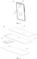
- FIG. 1 schematically shows a structure of an electronic device 10 according to an embodiment.
- an embodiment of this application provides the electronic device 10.
- the electronic device 10 may be a mobile terminal, a fixed terminal, or a foldable device, such as a monitor, a handheld wireless communication device, a desktop computer, a laptop (laptop) computer, a tablet (Tablet) computer, an ultra-mobile personal computer (ultra-mobile personal computer, UMPC), a handheld computer, a walkie-talkie, a netbook, a POS machine, or a personal digital assistant (personal digital assistant, PDA).
- a mobile terminal such as a monitor, a handheld wireless communication device, a desktop computer, a laptop (laptop) computer, a tablet (Tablet) computer, an ultra-mobile personal computer (ultra-mobile personal computer, UMPC), a handheld computer, a walkie-talkie, a netbook, a POS machine, or a personal digital assistant (personal digital assistant, PDA).
- PDA personal digital
- the handheld wireless communication device 10 may be a mobile phone.
- FIG. 2 schematically shows a breakdown structure of the electronic device 10 according to an embodiment.
- the electronic device 10 includes a display assembly 20, a middle frame 30, a circuit board assembly 40, and a rear cover 50.
- the display assembly 20 has a display region for displaying image information.
- the display region faces away from the middle frame 30. In a power-on state, the display region can display corresponding image information.
- the middle frame 30 is provided between the display assembly 20 and the rear cover 50 in a thickness direction of the electronic device 10. It should be noted that, the thickness direction of the electronic device 10 refers to an arrangement direction of the display assembly 20 and the rear cover 50.
- the circuit board assembly 40 is provided in a space formed between the middle frame 30 and the rear cover 50.
- the circuit board assembly 40 may be provided on a surface of the middle frame 30 that faces the rear cover 50.
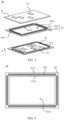
- FIG. 3 schematically shows a breakdown structure of the circuit board assembly 40 in a related technology.
- the circuit board assembly 40 may include circuit boards 41 and a plurality of electronic components 43 electrically connected to the circuit boards 41.
- the circuit board 41 in this application may be a printed circuit board (Printed Circuit Board, PCB), a flexible printed circuit (Flexible Printed Circuit, FPC), or an integrated circuit (or referred to as a chip).
- the circuit board 41 may be a single-sided board or double-sided board.
- Single-sided board means that the electronic components 43 are provided on one side of the circuit board 41.
- Double-sided board means that the electronic components 43 are provided on both sides of the circuit board 41.
- the circuit board 41 may be a radio frequency (radio frequency, RF) board or an application processor (application processor, AP) board.
- the radio frequency board may be configured to bear a radio frequency integrated circuit (radio frequency integrated circuit, RFIC), a radio frequency power amplifier (radio frequency power amplifier, RFPA), a wireless fidelity (wireless fidelity, Wi-Fi) chip, and the like, but is not limited thereto.
- the application processor board may be configured to bear a system on chip (system on chip, SOC) element, a double data rate (double data rate, DDR) memory, a primary power management unit (power management unit, PMU), a secondary power management unit, and the like, but is not limited thereto.
- the circuit board 41 may have a large lateral size, so that one circuit board 41 may be selected for use and a fixed quantity of electronic components 43 may be provided on the circuit board 41.
- the lateral size refers to a size measured in a direction perpendicular to the thickness direction of the electronic device 10. If the quantity and volumes of the electronic components 43 are large, a structure of the circuit board assembly 40 needs to be optimized when not all of the electronic components 43 can be accommodated on one circuit board 41. For example, a plurality of the circuit boards 41 are stacked along the thickness direction of the electronic device 10, and the electronic components 43 are provided on different circuit boards 41. In this way, an internal space of the electronic device 10 can be fully utilized along the thickness direction of the electronic device 10 to accommodate more and larger electronic components 43.
- FIG. 4 schematically shows a top-view structure of a frame plate shown in FIG. 3 .
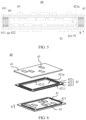
- FIG. 5 schematically shows a partial cross-sectional structure of the circuit board assembly 40 shown in FIG. 3 .
- the circuit board assembly 40 includes the circuit boards 41 and a frame plate 42. Two circuit boards 41 and the frame plate 42 are stacked along a thickness direction X of the frame plate 42.
- the frame plate 42 is provided between the two circuit boards 41.
- the two circuit boards 41 are separately connected to the frame plate 42, so that a predetermined distance is maintained between the two circuit boards 41 and locations of the two circuit boards 41 do not interfere with each other.
- the two circuit boards 41 may also be electrically connected to each other by using the frame plate 42, so that data information can be mutually transmitted between the two circuit boards 41.
- the frame plate 42 has an annular structure as a whole, so that the frame plate 42 includes a middle accommodating hole 421a.
- the frame plate 42 may have a polygonal structure, such as a rectangular structure.
- the frame plate 42 includes a frame body 421 and first soldering portions 422.
- the frame body 421 has the middle accommodating hole 421a and an outer wall 4211 and an inner wall 4212 that are opposite to each other.
- the outer wall 4211 of the frame body 421 refers to a region of the frame body 421 that faces away from the middle accommodating hole 421a.
- the inner wall 4212 of the frame body 421 refers to a region of the frame body 421 that faces the middle accommodating hole 421a.
- the width direction of the frame plate 42 refers to a direction from the outer wall 4211 to the inner wall 4212.
- the frame body 421 further has an intermediate region 4213 between the outer wall 4211 and the inner wall 4212.
- a material of the frame body 421 is an insulating material such as phenolic resin, epoxy resin, or polytetrafluoroethylene.
- the first soldering portions 422 are provided in the intermediate region 4213 of the frame body 421. A predetermined distance is maintained between the outer wall 4211 and the first soldering portions 422. A predetermined distance is also maintained between the inner wall 4212 and the first soldering portions 422. The first soldering portions 422 are exposed on two opposite surfaces of the frame body 421 along the thickness direction X of the frame plate 42.
- the circuit board 41 may be soldered to the first soldering portions 422 by using solder joints.
- a shape of the solder joint may be but is not limited to a spherical shape, an ellipsoidal shape, a cylindrical shape, or a truncated-cone shape.
- the first soldering portions 422 include functional pads and non-functional pads.
- the functional pads can play an electrical connection function and a mechanical fastening function. After the two circuit boards 41 are connected to the frame plate 42, the two circuit boards 41 can transmit electrical signals to each other by using the functional pads.
- the non-functional pads can play a mechanical fastening function, but the two circuit boards 41 cannot transmit electrical signals to each other by using the non-functional pads.
- the frame body 421 is provided with the non-functional pads in a region close to the outer wall 4211 or the inner wall 4212.
- the frame body 421 is an annular structure.
- a circle of non-functional pads close to the outer wall 4211 and a circle of non-functional pads close to the inner wall 4212 may be provided in the intermediate region 4213 of the frame body 421, and a circle of functional pads may be provided between the two circles of non-functional pads.
- Stability of a connection between the frame plate 42 and the circuit board 41 in the circuit board assembly 40 affects performance and a service life of the circuit board assembly 40. For example, when the electronic device 10 encounters an uneven force upon a drop, a collision, or the like, no fracture or separation can occur at a connection joint between the frame plate 42 and the circuit board 41 in the circuit board assembly 40. If a fracture or separation occurs at the connection joint between the frame plate 42 and the circuit board 41, the circuit board assembly 40 fails or malfunctions.
- the circuit board 41 is connected to the frame plate 42 by using the first soldering portions 422 provided in the intermediate region 4213 of the frame plate 42, but outer or inner edges of the circuit board 41 and the frame plate 42 are in a disconnected state.
- the circuit board 41 and the frame plate 42 together apply a shear force or a drawing force to the first soldering portions 422. Consequently, connection joints between the first soldering portions 422 and the solder joints or between the pads and the solder joints need to bear a large external force. As a result, the circuit board 422 is easily separated from the first soldering portions 422 or the frame plate 422 is easily separated from the first soldering portions 422.
- a width of the frame body 421 is properly increased to improve connection strength between the frame plate 42 and the circuit board 41, so that a larger quantity of first soldering portions 422 can be provided on the frame body 421, thereby increasing a connection force between the circuit board 41 and the frame plate 42.
- the connection force refers to a force that needs to be overcome for the circuit board 41 to be separated from the frame plate 42.
- the force required for separating the circuit board 41 from the frame plate 42 refers to a tensile stress, in a direction away from the frame plate 42, that is applied to the circuit board 41 along the thickness direction X of the frame plate 42 and that is required for separating the circuit board 41 from the frame plate 42.
- providing the second soldering portions 423 on the frame body 421 can increase the connection force between the frame plate 42 and the circuit board 41 without increasing the width of the frame body 421, thereby improving the stability and reliability of the connection between the frame plate 42 and the circuit board 41, and reducing a possibility of separation between the frame plate 42 and the circuit board 41 when the electronic device 10 encounters an uneven force upon a drop, a collision, or the like.
- circuit board assembly 40 provided in this embodiment of this application.
- FIG. 6 schematically shows a breakdown structure of the circuit board assembly 40 according to an embodiment of this application.
- FIG. 7 schematically shows a structure of a frame plate 42 in this embodiment of this application.
- the circuit board assembly 40 in this embodiment of this application is used in the electronic device 10.
- the circuit board assembly 40 includes the frame plate 42 and circuit boards 41.
- the frame plate 42 is a plateshaped structure with a predetermined thickness. In a thickness direction X of the frame plate 42, two circuit boards 41 are respectively provided on both sides of the frame plate 42, and the two circuit boards 41 are separately connected to the frame plate 42.
- the frame plate 42 is located between the two circuit boards 41.
- the frame plate 42 includes a frame body 421, first soldering portions 422, and second soldering portions 423.
- the frame body 421 has two surfaces that are opposite to each other along the thickness direction X.
- the frame body 421 includes a middle accommodating hole 421a that runs through both surfaces along the thickness direction X.
- the frame body 421 includes an outer wall 4211 and an inner wall 4212 that are provided opposite to each other along a width direction.
- the inner wall 4212 faces the middle accommodating hole 421a, and the outer wall 4211 faces away from the middle accommodating hole 421a.
- a region between the inner wall 4212 and the outer wall 4211 of the frame body 421 is an intermediate region 4213.
- the first soldering portions 422 are provided in the intermediate region 4213 of the frame body 421.
- FIG. 8 schematically shows a top-view structure of the frame body 421 according to an embodiment of this application. As shown in FIG. 8 and FIG.
- the accommodating grooves 4211a each have an opening facing away from the middle accommodating hole 421a.
- the accommodating grooves 4211a each have an opening facing the middle accommodating hole 421a.
- the accommodating grooves 4211a extend along the thickness direction X.
- the accommodating grooves 4211a may run through the two surfaces of the frame body 421 that are opposite to each other along the thickness direction X.
- the second soldering portions 423 are provided in the accommodating grooves 4211a and connected to the frame body 421. When the second soldering portions 423 are correspondingly provided in the accommodating grooves 4211a on the outer wall 4211, the second soldering portions 423 can be observed from an outer side of the frame plate 42. When the second soldering portions 423 are correspondingly provided in the accommodating grooves 4211a on the inner wall 4212, the second soldering portions 423 can be observed from an inner side of the frame plate 42.
- the circuit board 41 includes pads 411. The first soldering portions 422 and the second soldering portions 423 are respectively soldered to corresponding pads 411 on the circuit board 41.
- the circuit board assembly 40 in this embodiment of this application includes the frame plate 42 and the circuit boards 41.
- the frame plate 42 includes the frame body 421, the first soldering portions 422 located in the intermediate region 4213, and the second soldering portions 423 located on at least one of the outer wall 4211 and the inner wall 4212.
- density of connection points formed by the first soldering portions 422 and the second soldering portions 423 provided on the frame body 421 is higher.
- the circuit board 41 is connected to the frame plate 42 by using the first soldering portions 422 and the second soldering portions 423, so that edge regions of the circuit board 41 and the frame plate 42 are in a connected state.
- a connection force between the circuit board 41 and the frame plate 42 is increased due to an increase of the connection points between the circuit board 41 and the frame plate 42.
- the first soldering portions 422 and the second soldering portions 423 between the circuit board 41 and the frame plate 42 can buffer the force, thereby effectively reducing a possibility of separation between the circuit board 41 and the frame plate 42.
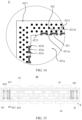
- FIG. 10 schematically shows a partial cross-sectional structure of the circuit board assembly 40 according to an embodiment of this application.
- the first soldering portions 422 and the second soldering portions 423 of the frame plate 42 are respectively soldered to the corresponding pads 411 on the circuit board 41 by using solder joints 60.
- materials of the first soldering portions 422 and the second soldering portions 423 may be copper or a copper alloy.
- a material of the pads 411 of the circuit board 41 may be copper or a copper alloy.
- solder paste is printed on the first soldering portions 422 and the second soldering portions 423 in advance.
- the solder paste may include tin and a solder flux.
- the circuit board 41 is provided on one side of the frame plate 42 and made to reach contact with the solder paste.
- the solder paste is heated and melted, so that the first soldering portions 422, the second soldering portions 423, and the pads 411 are all connected to the molten solder paste.
- the solder joints 60 are formed, so that the circuit board 41 is connected to the frame plate 42 by using the solder joints 60. Since the circuit board 41 is supported by the solder joints 60, a gap is formed between a surface of the circuit board 41 that faces the frame plate 42 and a surface of the frame plate 42 that faces the circuit board 41. For example, along the thickness direction X, the solder joints 60 are provided between the first soldering portions 422 and the pads 411, and between the second soldering portions 423 and the pads 411.
- FIG. 11 schematically shows a top-view structure of the frame body 421 according to an embodiment of this application.
- the frame plate 42 is an annular structure, for example, a rectangular structure.
- two or more accommodating grooves 4211a are provided on the outer wall 4211 of the frame body 421, and the two or more accommodating grooves 4211a are evenly distributed, so that a spacing between every two adjacent accommodating grooves 4211a is equal.
- the accommodating grooves 4211a may be formed on the frame body 421 through processing in a finish machining manner, for example, by using a drilling tool or a milling cutter.
- the circumferential direction of the frame plate 42 refers to a direction around the middle accommodating hole 421a.
- a quantity and locations of the second soldering portions 423 one-to-one correspond to a quantity and locations of the accommodating grooves 4211a.
- Two or more second soldering portions 423 are also evenly distributed along the circumferential direction of the frame plate 42. Therefore, soldering all the second soldering portions 423 to the corresponding pads 411 on the circuit board 41 is advantageous to improving a force balance of the circuit board 41 at each location, and reducing a possibility of local warpage of the circuit board 41 due to an unbalanced connection force between the circuit board 41 and the frame plate 42 at different locations.
- FIG. 13 schematically shows a top-view structure of the frame plate 42 according to an embodiment of this application.
- two or more accommodating grooves 4211a are provided on the inner wall 4212 of the frame body 421, and the two or more accommodating grooves 4211a are evenly distributed, so that a spacing between every two adjacent accommodating grooves 4211a is equal.
- the accommodating grooves 4211a may be formed on the frame body 421 through processing in a finish machining manner, for example, by using a drilling tool or a milling cutter.
- a quantity and locations of the second soldering portions 423 one-to-one correspond to a quantity and locations of the accommodating grooves 4211a.
- Two or more second soldering portions 423 are also evenly distributed along the circumferential direction of the frame plate 42. Therefore, soldering all the second soldering portions 423 to the corresponding pads 411 on the circuit board 41 is advantageous to improving a force balance of the circuit board 41 at each location, and reducing a possibility of local warpage of the circuit board 41 due to an unbalanced connection force between the circuit board 41 and the frame plate 42 at different locations.
- FIG. 15 schematically shows a partial cross-sectional structure of the circuit board assembly 40 according to an embodiment of this application.
- the second soldering portions 423 provided on the inner wall 4212 are connected to the corresponding pads 411 on the circuit board 41 by using the solder joints 60, so that an inner edge of the frame plate 42 is connected to the circuit board 41.
- the first soldering portions 422 provided in the intermediate region 4213 and the second soldering portions 423 provided on the inner wall 4212 are all connected to the circuit board 41. This improves connection strength between the circuit board 41 and the frame plate 42, and helps improve stability and reliability of the connection between the circuit board 41 and the frame plate 42.
- FIG. 16 schematically shows a top-view structure of the frame plate 42 according to an embodiment of this application.
- the inner wall 4212 and the outer wall 4211 of the frame body 421 each are provided with the accommodating grooves 4211a, so that the second soldering portion 423 is provided in each accommodating groove 4211a.
- the second soldering portions 423 in the accommodating grooves 4211a on the inner wall 4212 of the frame body 421 may be soldered to the corresponding pads 411 on the circuit board 41, so that an inner edge of the frame plate 42 is connected to the circuit board 41.
- the second soldering portions 423 in the accommodating grooves 4211a on the outer wall 4211 of the frame body 421 may be soldered to the corresponding pads 411 on the circuit board 41, so that an outer edge of the frame plate 42 is connected to the circuit board 41. Therefore, both the inner edge and the outer edge of the frame plate 42 can be connected to the circuit board 41. This further helps increase the connection force between the circuit board 41 and the frame plate 42, and improve the stability and reliability of the connection between the circuit board 41 and the frame plate 42.
- the quantity and locations of the accommodating grooves 4211a on the outer wall 4211 one-to-one correspond to the quantity and locations of the accommodating grooves 4211a on the inner wall 4212, so that the accommodating grooves 4211a on the outer wall 4211 correspond to the accommodating grooves 4211a on the inner wall 4212 along the width direction of the frame plate 42.
- the accommodating grooves 4211a on the outer wall 4211 may be staggered from the accommodating grooves 4211a on the inner wall 4212, so that one accommodating groove 4211a on the outer wall 4211 corresponds to a region between two accommodating grooves 4211a on the inner wall 4212 along the width direction of the frame plate 42.
- through holes 4211b are provided in the intermediate region 4213 of the frame body 421.
- the through holes 4211b run through the two opposite surfaces of the frame body 421 along the thickness direction X of the frame plate 42.
- the first soldering portions 422 are correspondingly provided in the through holes 4211b.
- the through holes 4211b are circular holes.
- the through holes 4211b may be formed on the frame body 421 through processing in a finish machining manner, for example, by drilling.
- the intermediate region 4213 of the frame body 421 is provided with two or more rows of through holes 4211b.
- Each through hole 4211b is correspondingly provided with the first soldering portion 422, so that two or more rows of first soldering portions 422 are formed correspondingly.
- the two or more rows of through holes 4211b are spaced along the width direction of the frame plate 42.
- the outer wall 4211 of the frame body 421 is provided with accommodating grooves 4211a
- one accommodating groove 4211a on the outer wall 4211 is provided corresponding to two through holes 4211b, so that one second soldering portion 423 is provided corresponding to two first soldering portions 422.
- one accommodating groove 4211a on the inner wall 4212 is provided corresponding to two through holes 4211b, so that one second soldering portion 423 is provided corresponding to two first soldering portions 422.
- a connection point formed by the second soldering portion 423 and the pad 411 and connection points formed by the first soldering portions 422 and the pads 411 form a triangular layout, which helps improve the stability of the connection between the circuit board 41 and the frame plate 42.
- neither of the two first soldering portions 422 respectively exceed edges of the corresponding second soldering portion 423.
- a quantity and locations of the accommodating grooves 4211a on the outer wall 4211 one-to-one correspond to a quantity and locations of the accommodating grooves 4211a on the inner wall 4212.
- Three rows of through holes 4211b are provided in the intermediate region 4213 of the frame plate 42. Along the width direction of the frame plate 42, centers of the one row of through holes 4211b close to the outer wall 4211 are aligned with centers of the one row of through holes 4211b close to the inner wall 4212. The centers of the one row of through holes 4211b close to the outer wall 4211 and centers of one row of through holes 4211b in the middle are staggered from each other.
- the centers of the one row of through holes 4211b close to the inner wall 4212 are also staggered from the centers of the one row of through holes 4211b in the middle.
- the first soldering portions 422 provided in the one row of through holes 4211b close to the outer wall 4211 and the one row of through holes 4211b close to the inner wall 4212 may serve as non-functional pads
- the first soldering portions 422 provided in the one row of through holes 4211b in the middle may serve as functional pads.
- a quantity and locations of the accommodating grooves 4211a on the outer wall 4211 one-to-one correspond to a quantity and locations of the accommodating grooves 4211a on the inner wall 4212.
- Two rows of through holes 4211b are provided in the intermediate region 4213 of the frame plate 42. Along the width direction of the frame plate 42, centers of one row of through holes 4211b are aligned with centers of the other row of through holes 4211b.
- the first soldering portions 422 provided in the one row of through holes 4211b may serve as non-functional pads, and the first soldering portions 422 provided in the other row of through holes 4211b may serve as functional pads.
- the accommodating groove 4211a includes a bottom surface 4211aa and side surfaces 4211ab.
- the bottom surface 4211aa of the accommodating groove 4211a intersects the side surfaces 4211ab thereof.
- an included angle between the bottom surface 4211aa and the side surface 4211ab of the accommodating groove 4211a may range from 90° to 110°.
- a depth of the accommodating groove 4211a may be, but is not limited to, 0.2 mm.
- the depth of the accommodating groove 4211a refers to a vertical distance from the bottom surface 4211aa to an opening of the accommodating groove 4211a.
- a shape of a surface of the second soldering portion 423 that faces the bottom surface 4211aa matches a shape of the bottom surface 4211aa.
- a shape of a surface of the second soldering portion 423 that faces the side surface 4211ab matches a shape of the side surface 4211ab. Therefore, the surface of the second soldering portion 423 that faces the accommodating groove 4211a can fit tightly with the surface of the accommodating groove 4211a.
- surfaces of the second soldering portion 423 that face away from the middle accommodating hole 421a include a first concave surface 423a, a second concave surface 423b, and a third concave surface 423c. Regions corresponding to the first concave surface 423a, the second concave surface 423b, and the third concave surface 423c may be configured to avoid the electronic components 43.
- the first concave surface 423a, the second concave surface 423b, and the third concave surface 423c are depressed towards the intermediate region 4213.
- the second concave surface 423b and the third concave surface 423c are respectively located on both sides of the first concave surface 423a along the circumferential direction of the frame plate 42.
- An intersecting region between the first concave surface 423a and the second concave surface 423b and an intersecting region between the first concave surface 423a and the third concave surface 423c both exceed the opening of the accommodating groove 4211a.
- the region between the first concave surface 423a and the second concave surface 423b and the region between the first concave surface 423a and the third concave surface 423c are thin in size and form relatively sharp structures, and therefore are easily broken when subjected to impact of an external force.
- the depression depth of the second concave surface 423b and the depression depth of the third concave surface 423c each are less than the depression depth of the first concave surface 423a.
- the first concave surface 423a, the second concave surface 423b, and the third concave surface 423c are all arc surfaces.
- a central angle corresponding to the first concave surface 423a is 60° to 120°.
- the first concave surface 423a, the second concave surface 423b, and the third concave surface 423c have a same radius.
- the first concave surface 423a, the second concave surface 423b, and the third concave surface 423c are processed and manufactured by drilling or milling, it is convenient to use a tool with one diameter for cutting. This reduces a possibility that a processing operation is complex and processing efficiency is low due to a need of replacing tools with different diameters.
- FIG. 19 schematically shows a partial cross-sectional structure of the circuit board assembly 40 according to an embodiment of this application.
- the second soldering portions 423 on the outer wall 4211 and the inner wall 4212 are respectively connected to the corresponding pads 411 on the circuit board 41 by using the solder joints 60, so that both the outer edge and the inner edge of the frame plate 42 are connected to the circuit board 41.
- the first soldering portions 422 provided in the intermediate region 4213 and the second soldering portions 423 provided on the outer wall 4211 and the inner wall 4212 are all connected to the circuit board 41. This improves connection strength between the circuit board 41 and the frame plate 42, and helps improve stability and reliability of the connection between the circuit board 41 and the frame plate 42.
- FIG. 20 schematically shows a procedure of a manufacturing method for the frame plate 42 according to an embodiment of this application. As shown in FIG. 20 , an embodiment of this application further provides a manufacturing method for the frame plate 42. The manufacturing method includes the following steps:
- the copper clad layer 101 and the second copper layer 700 on the surface of the copper clad layer 101 are patterned by using an alkaline etching solution in an etching process, to form corresponding routes.
- the finish machining-based contour processing process may be drilling or milling.
- the frame plate 42 with the predetermined shape may be rectangular or square.
- the manufacturing method for the frame plate 42 in this embodiment of this application is used to manufacture the frame plate 42 in the foregoing embodiments.
- connection may be a fixed connection, an indirect connection through an intermediate medium, internal communication between two elements, or an interaction relationship between two elements.
- connection may be a fixed connection, an indirect connection through an intermediate medium, internal communication between two elements, or an interaction relationship between two elements.
- a plurality of in this specification refers to two or more.
- the term “and/or” in this specification describes only an association relationship for describing associated objects and represents that three relationships can exist. For example, “A and/or B” can represent the following three cases: Only A exists, both A and B exist, and only B exists.
- the character “/” in this specification generally indicates an "or” relationship between the associated objects. In a formula, the character “/” indicates that the associated objects are in a "division" relationship.
- sequence number of each of the foregoing processes does not mean a sequence of execution.
- the sequence of execution of the processes should be determined based on functions and internal logic of the processes, and no limitation should be imposed on an implementation process of the embodiments of this application.
Landscapes
- Engineering & Computer Science (AREA)
- Microelectronics & Electronic Packaging (AREA)
- Manufacturing & Machinery (AREA)
- Combinations Of Printed Boards (AREA)
- Mounting Of Printed Circuit Boards And The Like (AREA)
Abstract
Description
- This application claims priority to
Chinese Patent Application No. 202111117615.9, filed with the China National Intellectual Property Administration on September 23, 2021 - Embodiments of this application relate to the field of terminal technologies, and in particular, to a circuit board assembly and an electronic device.
- As electronic products develop towards the direction of high-density packaging, at present, a plurality of circuit boards are usually stacked to provide a larger arrangement space for a battery and other functional modules in the electronic devices. In the manner of stacking a plurality of circuit boards, electronic components may be scattered on the circuit boards. In this way, all the electronic components can be arranged without increasing areas of the circuit boards that bear the electronic components.
- In the manner of stacking a plurality of circuit boards, two adjacent circuit boards are connected by using a frame plate. The frame plate and the circuit boards are assembled by soldering to form a circuit board assembly. Different circuit boards may be electrically connected to each other by using a frame plate to implement data information exchange. Because a circuit board and a frame plate are two mechanical parts designed separately, the circuit board and the frame plate are easily separated at a connection joint in a scenario with an uneven force such as a drop or a collision of an electronic device, causing a communication failure or malfunction of a circuit board assembly.
- Embodiments of this application provide a circuit board assembly and an electronic device, which can increase a connection force between a circuit board and a frame plate, and effectively reduce a possibility of separation between the circuit board and the frame plate.
- A first aspect of this application provides a circuit board assembly. The circuit board assembly is used in an electronic device. The circuit board assembly includes at least a frame plate and circuit boards. The frame plate includes a frame body, first soldering portions, and second soldering portions. The frame body has a middle accommodating hole, an inner wall facing the middle accommodating hole, and an outer wall facing away from the middle accommodating hole. The first soldering portions are provided in an intermediate region located on the frame body between the inner wall and the outer wall. At least one of the inner wall and the outer wall is provided with accommodating grooves. The accommodating grooves extend along a thickness direction of the frame plate. The second soldering portions are provided in the accommodating grooves and connected to the frame body. Two circuit boards are respectively provided on two opposite sides of the frame plate along the thickness direction. The circuit board includes pads. The first soldering portions and the second soldering portions are soldered to corresponding pads, respectively.
- The circuit board assembly in this embodiment of this application includes the frame plate and the circuit boards. The frame plate includes the frame body, the first soldering portions located in the intermediate region, and the second soldering portions located on at least one of the outer wall and the inner wall. When a width of the frame body can be kept unchanged, density of connection points formed by the first soldering portions and the second soldering portions provided on the frame body is higher. The circuit board is connected to the frame plate by using the first soldering portions and the second soldering portions, so that edge regions of the circuit board and the frame plate are in a connected state. In addition, a connection force between the circuit board and the frame plate is increased due to an increase of the connection points between the circuit board and the frame plate. When the circuit board assembly encounters an uneven force upon a drop, a collision, or the like, the first soldering portions and the second soldering portions between the circuit board and the frame plate can buffer the force, thereby effectively reducing a possibility of separation between the circuit board and the frame plate.
- In a possible implementation, the accommodating groove includes a bottom surface and side surfaces. The bottom surface intersects the side surfaces. A shape of a surface of the second soldering portion that faces the bottom surface matches a shape of the bottom surface. A shape of a surface of the second soldering portion that faces the side surface matches a shape of the side surface. The surface of the second soldering portion that faces the accommodating groove can fit tightly with the surface of the accommodating groove. This helps increase a bonding force between the surface of the second soldering portion and the surface of the accommodating groove, and reduce a possibility that the circuit board fails to be connected to the frame plate by using the second soldering portion due to separation between the surface of the second soldering portion and the surface of accommodating groove.
- In a possible implementation, an included angle between the bottom surface and the side surface of the accommodating groove may range from 90° to 110°.
- In a possible implementation, the accommodating groove runs through two surfaces of the frame body that are opposite to each other along the thickness direction.
- In a possible implementation, the first soldering portions and the second soldering portions are respectively soldered to the corresponding pads on the circuit board by using solder joints.
- In a possible implementation, surfaces of the second soldering portion that face away from the middle accommodating hole include a first concave surface, a second concave surface, and a third concave surface. The first concave surface, the second concave surface, and the third concave surface are depressed towards the intermediate region. The second concave surface and the third concave surface are respectively located on both sides of the first concave surface along a circumferential direction of the frame plate. An intersecting region between the first concave surface and the second concave surface and an intersecting region between the first concave surface and the third concave surface both exceed an opening of the accommodating groove.
- In a possible implementation, a depression depth of the second concave surface and a depression depth of the third concave surface each are less than a depression depth of the first concave surface.
- In a possible implementation, the first concave surface, the second concave surface, and the third concave surface are all arc surfaces.
- In a possible implementation, a central angle corresponding to the first concave surface is 60° to 120°.
- In a possible implementation, the first concave surface, the second concave surface, and the third concave surface have a same radius. When the first concave surface, the second concave surface, and the third concave surface are processed and manufactured by drilling or milling, it is convenient to use a tool with one diameter for cutting. This reduces a possibility that a processing operation is complex and processing efficiency is low due to a need of replacing tools with different diameters.
- In a possible implementation, along the circumferential direction of the frame plate, two or more accommodating grooves are evenly distributed, and two or more second soldering portions are evenly distributed. A spacing between every two adjacent accommodating grooves is equal. A quantity and locations of the second soldering portions one-to-one correspond to a quantity and locations of the accommodating grooves. Two or more second soldering portions are also evenly distributed along the circumferential direction of the frame plate. Therefore, soldering all the second soldering portions to the corresponding pads on the circuit board is advantageous to improving a force balance of the circuit board at each location, and reducing a possibility of local warpage of the circuit board due to an unbalanced connection force between the circuit board and the frame plate at different locations.
- In a possible implementation, the inner wall and the outer wall each are provided with the accommodating grooves, so that the second soldering portion is provided in each accommodating groove. This further helps increase the density of the connection points formed by the first soldering portions and the second soldering portions provided on the frame plate.
- In a possible implementation, a quantity and locations of the accommodating grooves on the outer wall one-to-one correspond to a quantity and locations of the accommodating grooves on the inner wall.
- In a possible implementation, two or more rows of through holes are provided in the intermediate region. Each of the through holes is correspondingly provided with the first soldering portion. The two or more rows of through holes are spaced along a width direction of the frame plate. In one row of the through holes close to the outer wall, one of the accommodating grooves on the outer wall is provided corresponding to two of the through holes. In one row of the through holes close to the inner wall, one of the accommodating grooves on the inner wall is provided corresponding to two of the through holes.
- A second aspect of the embodiments of this application provides an electronic device. The electronic device includes the circuit board assembly described above.
- The circuit board assembly includes at least a frame plate and circuit boards. The frame plate includes a frame body, first soldering portions, and second soldering portions. The frame body has a middle accommodating hole, an inner wall facing the middle accommodating hole, and an outer wall facing away from the middle accommodating hole. The first soldering portions are provided in an intermediate region located on the frame body between the inner wall and the outer wall. At least one of the inner wall and the outer wall is provided with accommodating grooves. The accommodating grooves extend along a thickness direction of the frame plate. The second soldering portions are provided in the accommodating grooves and connected to the frame body. Two circuit boards are respectively provided on two opposite sides of the frame plate along the thickness direction. The circuit board includes pads. The first soldering portions and the second soldering portions are soldered to corresponding pads, respectively.
- In a possible implementation, the accommodating groove includes a bottom surface and side surfaces. The bottom surface intersects the side surfaces. A shape of a surface of the second soldering portion that faces the bottom surface matches a shape of the bottom surface. A shape of a surface of the second soldering portion that faces the side surface matches a shape of the side surface. The surface of the second soldering portion that faces the accommodating groove can fit tightly with the surface of the accommodating groove. This helps increase a bonding force between the surface of the second soldering portion and the surface of the accommodating groove, and reduce a possibility that the circuit board fails to be connected to the frame plate by using the second soldering portion due to separation between the surface of the second soldering portion and the surface of accommodating groove.
- In a possible implementation, an included angle between the bottom surface and the side surface of the accommodating groove may range from 90° to 110°.
- In a possible implementation, the accommodating groove runs through two surfaces of the frame body that are opposite to each other along the thickness direction.
- In a possible implementation, the first soldering portions and the second soldering portions are respectively soldered to the corresponding pads on the circuit board by using solder joints.
- In a possible implementation, surfaces of the second soldering portion that face away from the middle accommodating hole include a first concave surface, a second concave surface, and a third concave surface. The first concave surface, the second concave surface, and the third concave surface are depressed towards the intermediate region. The second concave surface and the third concave surface are respectively located on both sides of the first concave surface along a circumferential direction of the frame plate. An intersecting region between the first concave surface and the second concave surface and an intersecting region between the first concave surface and the third concave surface both exceed an opening of the accommodating groove.
- In a possible implementation, a depression depth of the second concave surface and a depression depth of the third concave surface each are less than a depression depth of the first concave surface.
- In a possible implementation, the first concave surface, the second concave surface, and the third concave surface are all arc surfaces.
- In a possible implementation, a central angle corresponding to the first concave surface is 60° to 120°.
- In a possible implementation, the first concave surface, the second concave surface, and the third concave surface have a same radius. When the first concave surface, the second concave surface, and the third concave surface are processed and manufactured by drilling or milling, it is convenient to use a tool with one diameter for cutting. This reduces a possibility that a processing operation is complex and processing efficiency is low due to a need of replacing tools with different diameters.
- In a possible implementation, along the circumferential direction of the frame plate, two or more accommodating grooves are evenly distributed, and two or more second soldering portions are evenly distributed. A spacing between every two adjacent accommodating grooves is equal. A quantity and locations of the second soldering portions one-to-one correspond to a quantity and locations of the accommodating grooves. Two or more second soldering portions are also evenly distributed along the circumferential direction of the frame plate. Therefore, soldering all the second soldering portions to the corresponding pads on the circuit board is advantageous to improving a force balance of the circuit board at each location, and reducing a possibility of local warpage of the circuit board due to an unbalanced connection force between the circuit board and the frame plate at different locations.
- In a possible implementation, the inner wall and the outer wall each are provided with the accommodating grooves, so that the second soldering portion is provided in each accommodating groove. This further helps increase the density of the connection points formed by the first soldering portions and the second soldering portions provided on the frame plate.
- In a possible implementation, a quantity and locations of the accommodating grooves on the outer wall one-to-one correspond to a quantity and locations of the accommodating grooves on the inner wall.
- In a possible implementation, two or more rows of through holes are provided in the intermediate region. Each of the through holes is correspondingly provided with the first soldering portion. The two or more rows of through holes are spaced along a width direction of the frame plate. In one row of the through holes close to the outer wall, one of the accommodating grooves on the outer wall is provided corresponding to two of the through holes. In one row of the through holes close to the inner wall, one of the accommodating grooves on the inner wall is provided corresponding to two of the through holes.
- A third aspect of the embodiments of this application provides a manufacturing method for a frame plate. The manufacturing method includes the following steps:
- A copper clad substrate is provided, where the copper clad substrate includes a dielectric layer and copper clad layers on both sides.
- A hole is drilled in the copper clad substrate to form a first via.
- A first copper layer is formed on an inner wall of the first via, and the first copper layer is electrically connected to the copper clad layers on both sides.
- A central hole of the first copper layer is filled with a resin block.
- A hole is drilled in the copper clad substrate to form a second via, where the first via and the second via are spaced apart.
- An anti-electroplating film is provided on a surface of the copper clad layer.
- A second copper layer is formed on an inner wall of the second via and on the surface of the copper clad layer by successively using a chemical plating process and an electroplating process.
- The anti-electroplating film is removed.
- The copper clad layer and the second copper layer on the surface of the copper clad layer are patterned by using an etching process.
- A solder-resist material layer is provided in an etched region.
- The copper-clad substrate is cut into a frame plate with a predetermined shape by using a finish machining-based contour processing process. After the processing is completed, portions of the second via and the second copper layer are cut off. The first via forms a through hole, and the copper clad layer, the first copper layer, and the second copper layer that correspond to the first via form a first soldering portion. A remaining portion of the second via forms an accommodating groove, and the copper clad layer and the second copper layer that correspond to the remaining portion of the second via form a second soldering portion.
-
-
FIG. 1 is a schematic diagram of a structure of an electronic device according to an embodiment of this application; -
FIG. 2 is a schematic diagram of a breakdown structure of an electronic device according to an embodiment of this application; -
FIG. 3 is a schematic diagram of a breakdown structure of a circuit board assembly according to a related technology; -
FIG. 4 is a schematic diagram of a top-view structure of a frame plate in the embodiment shown inFIG. 3 ; -
FIG. 5 is a schematic diagram of a cross-sectional structure of the circuit board assembly in the embodiment shown inFIG. 3 ; -
FIG. 6 is a schematic diagram of a breakdown structure of a circuit board assembly according to an embodiment of this application; -
FIG. 7 is a schematic diagram of a structure of a frame plate according to an embodiment of this application; -
FIG. 8 is a schematic diagram of a top-view structure of a frame body according to an embodiment of this application; -
FIG. 9 is an enlarged view of a location A inFIG. 8 ; -
FIG. 10 is a schematic diagram of a cross-sectional structure of a circuit board assembly according to an embodiment of this application; -
FIG. 11 is a schematic diagram of a top-view structure of a frame plate according to an embodiment of this application; -
FIG. 12 is an enlarged view of a location B inFIG. 11 ; -
FIG. 13 is a schematic diagram of a top-view structure of a frame plate according to another embodiment of this application; -
FIG. 14 is an enlarged view of a location C inFIG. 13 ; -
FIG. 15 is a schematic diagram of a cross-sectional structure of a circuit board assembly according to another embodiment of this application; -
FIG. 16 is a schematic diagram of a top-view structure of a frame plate according to still another embodiment of this application; -
FIG. 17 is an enlarged view of a location D inFIG. 16 ; -
FIG. 18 is a schematic diagram of a local structure of a frame plate according to another embodiment of this application; -
FIG. 19 is a schematic diagram of a cross-sectional structure of a circuit board assembly according to still another embodiment of this application; and -
FIG. 20 is a schematic diagram of a manufacturing method for a frame plate according to an embodiment of this application. - Description of reference numerals:
- 10: electronic device;
- 20: display assembly;
- 30: middle frame;
- 40: circuit board assembly;
- 41: circuit board; and 411: pad;
- 42: frame plate;
421: frame body; 421a: middle accommodating hole; 4211: outer wall; - 4211a: accommodating groove; 4211aa: bottom surface; 4211ab: side surface; 4211b: through hole; 4212: inner wall; and 4213: intermediate region;
- 422: first soldering portion;
- 423: second soldering portion; 423a: first concave surface; 423b: second concave surface; and 423c: third concave surface;
- 43: electronic component;
- 50: rear cover;
- 60: solder joint;
- 100: copper clad substrate; 101: copper clad layer; and 102: dielectric layer;
- 200: first via;
- 300: first copper layer;
- 400: resin block;
- 500: second via;
- 600: anti-electroplating film;
- 700: second copper layer;
- 800: solder-resist material layer; and
- X: thickness direction.
-
FIG. 1 schematically shows a structure of anelectronic device 10 according to an embodiment. As shown inFIG. 1 , an embodiment of this application provides theelectronic device 10. Theelectronic device 10 may be a mobile terminal, a fixed terminal, or a foldable device, such as a monitor, a handheld wireless communication device, a desktop computer, a laptop (laptop) computer, a tablet (Tablet) computer, an ultra-mobile personal computer (ultra-mobile personal computer, UMPC), a handheld computer, a walkie-talkie, a netbook, a POS machine, or a personal digital assistant (personal digital assistant, PDA). - For ease of description, an example in which the
electronic device 10 is a handheld wireless communication device is used for description in all of the following embodiments. The handheld wireless communication device may be a mobile phone. -
FIG. 2 schematically shows a breakdown structure of theelectronic device 10 according to an embodiment. As shown inFIG. 2 , theelectronic device 10 includes adisplay assembly 20, amiddle frame 30, acircuit board assembly 40, and arear cover 50. Thedisplay assembly 20 has a display region for displaying image information. The display region faces away from themiddle frame 30. In a power-on state, the display region can display corresponding image information. Themiddle frame 30 is provided between thedisplay assembly 20 and therear cover 50 in a thickness direction of theelectronic device 10. It should be noted that, the thickness direction of theelectronic device 10 refers to an arrangement direction of thedisplay assembly 20 and therear cover 50. Thecircuit board assembly 40 is provided in a space formed between themiddle frame 30 and therear cover 50. Thecircuit board assembly 40 may be provided on a surface of themiddle frame 30 that faces therear cover 50. -
FIG. 3 schematically shows a breakdown structure of thecircuit board assembly 40 in a related technology. As shown inFIG. 3 , thecircuit board assembly 40 may includecircuit boards 41 and a plurality ofelectronic components 43 electrically connected to thecircuit boards 41. - The
circuit board 41 in this application may be a printed circuit board (Printed Circuit Board, PCB), a flexible printed circuit (Flexible Printed Circuit, FPC), or an integrated circuit (or referred to as a chip). Thecircuit board 41 may be a single-sided board or double-sided board. "Single-sided board" means that theelectronic components 43 are provided on one side of thecircuit board 41. "Double-sided board" means that theelectronic components 43 are provided on both sides of thecircuit board 41. Thecircuit board 41 may be a radio frequency (radio frequency, RF) board or an application processor (application processor, AP) board. The radio frequency board may be configured to bear a radio frequency integrated circuit (radio frequency integrated circuit, RFIC), a radio frequency power amplifier (radio frequency power amplifier, RFPA), a wireless fidelity (wireless fidelity, Wi-Fi) chip, and the like, but is not limited thereto. For example, the application processor board may be configured to bear a system on chip (system on chip, SOC) element, a double data rate (double data rate, DDR) memory, a primary power management unit (power management unit, PMU), a secondary power management unit, and the like, but is not limited thereto. - For example, when a thickness of the
electronic device 10 is small but thedisplay assembly 20 is large, thecircuit board 41 may have a large lateral size, so that onecircuit board 41 may be selected for use and a fixed quantity ofelectronic components 43 may be provided on thecircuit board 41. The lateral size refers to a size measured in a direction perpendicular to the thickness direction of theelectronic device 10. If the quantity and volumes of theelectronic components 43 are large, a structure of thecircuit board assembly 40 needs to be optimized when not all of theelectronic components 43 can be accommodated on onecircuit board 41. For example, a plurality of thecircuit boards 41 are stacked along the thickness direction of theelectronic device 10, and theelectronic components 43 are provided ondifferent circuit boards 41. In this way, an internal space of theelectronic device 10 can be fully utilized along the thickness direction of theelectronic device 10 to accommodate more and largerelectronic components 43. -
FIG. 4 schematically shows a top-view structure of a frame plate shown inFIG. 3 .FIG. 5 schematically shows a partial cross-sectional structure of thecircuit board assembly 40 shown inFIG. 3 . As shown inFIG. 4 andFIG. 5 , in the related technology, thecircuit board assembly 40 includes thecircuit boards 41 and aframe plate 42. Twocircuit boards 41 and theframe plate 42 are stacked along a thickness direction X of theframe plate 42. Theframe plate 42 is provided between the twocircuit boards 41. The twocircuit boards 41 are separately connected to theframe plate 42, so that a predetermined distance is maintained between the twocircuit boards 41 and locations of the twocircuit boards 41 do not interfere with each other. The twocircuit boards 41 may also be electrically connected to each other by using theframe plate 42, so that data information can be mutually transmitted between the twocircuit boards 41. Theframe plate 42 has an annular structure as a whole, so that theframe plate 42 includes a middleaccommodating hole 421a. For example, theframe plate 42 may have a polygonal structure, such as a rectangular structure. After the twocircuit boards 41 are connected to theframe plate 42, theelectronic components 43 on the twocircuit boards 41 may be located in the middleaccommodating hole 421a, to avoid locations of theframe plate 42 and theelectronic components 43 interfere with each other. A thickness of theframe plate 42 needs to ensure that theelectronic components 43 that are located in the middleaccommodating hole 421a and that are located on the twocircuit boards 41 do not reach contact with each other. - In some implementations, the
frame plate 42 includes aframe body 421 andfirst soldering portions 422. Along a width direction of theframe plate 42, theframe body 421 has the middleaccommodating hole 421a and anouter wall 4211 and aninner wall 4212 that are opposite to each other. It should be noted that, theouter wall 4211 of theframe body 421 refers to a region of theframe body 421 that faces away from the middleaccommodating hole 421a. Theinner wall 4212 of theframe body 421 refers to a region of theframe body 421 that faces the middleaccommodating hole 421a. The width direction of theframe plate 42 refers to a direction from theouter wall 4211 to theinner wall 4212. Theframe body 421 further has anintermediate region 4213 between theouter wall 4211 and theinner wall 4212. A material of theframe body 421 is an insulating material such as phenolic resin, epoxy resin, or polytetrafluoroethylene. Thefirst soldering portions 422 are provided in theintermediate region 4213 of theframe body 421. A predetermined distance is maintained between theouter wall 4211 and thefirst soldering portions 422. A predetermined distance is also maintained between theinner wall 4212 and thefirst soldering portions 422. Thefirst soldering portions 422 are exposed on two opposite surfaces of theframe body 421 along the thickness direction X of theframe plate 42. - The
circuit board 41 may be soldered to thefirst soldering portions 422 by using solder joints. A shape of the solder joint may be but is not limited to a spherical shape, an ellipsoidal shape, a cylindrical shape, or a truncated-cone shape. Thefirst soldering portions 422 include functional pads and non-functional pads. The functional pads can play an electrical connection function and a mechanical fastening function. After the twocircuit boards 41 are connected to theframe plate 42, the twocircuit boards 41 can transmit electrical signals to each other by using the functional pads. The non-functional pads can play a mechanical fastening function, but the twocircuit boards 41 cannot transmit electrical signals to each other by using the non-functional pads. - In some implementations, the
frame body 421 is provided with the non-functional pads in a region close to theouter wall 4211 or theinner wall 4212. For example, theframe body 421 is an annular structure. A circle of non-functional pads close to theouter wall 4211 and a circle of non-functional pads close to theinner wall 4212 may be provided in theintermediate region 4213 of theframe body 421, and a circle of functional pads may be provided between the two circles of non-functional pads. - Stability of a connection between the
frame plate 42 and thecircuit board 41 in thecircuit board assembly 40 affects performance and a service life of thecircuit board assembly 40. For example, when theelectronic device 10 encounters an uneven force upon a drop, a collision, or the like, no fracture or separation can occur at a connection joint between theframe plate 42 and thecircuit board 41 in thecircuit board assembly 40. If a fracture or separation occurs at the connection joint between theframe plate 42 and thecircuit board 41, thecircuit board assembly 40 fails or malfunctions. However, in the related technology, thecircuit board 41 is connected to theframe plate 42 by using thefirst soldering portions 422 provided in theintermediate region 4213 of theframe plate 42, but outer or inner edges of thecircuit board 41 and theframe plate 42 are in a disconnected state. Therefore, when theelectronic device 10 encounters a drop or a collision, thecircuit board 41 and theframe plate 42 together apply a shear force or a drawing force to thefirst soldering portions 422. Consequently, connection joints between thefirst soldering portions 422 and the solder joints or between the pads and the solder joints need to bear a large external force. As a result, thecircuit board 422 is easily separated from thefirst soldering portions 422 or theframe plate 422 is easily separated from thefirst soldering portions 422. In some related technologies, a width of theframe body 421 is properly increased to improve connection strength between theframe plate 42 and thecircuit board 41, so that a larger quantity offirst soldering portions 422 can be provided on theframe body 421, thereby increasing a connection force between thecircuit board 41 and theframe plate 42. It should be noted that, the connection force refers to a force that needs to be overcome for thecircuit board 41 to be separated from theframe plate 42. The force required for separating thecircuit board 41 from theframe plate 42 refers to a tensile stress, in a direction away from theframe plate 42, that is applied to thecircuit board 41 along the thickness direction X of theframe plate 42 and that is required for separating thecircuit board 41 from theframe plate 42. However, when the width of theframe body 421 is designed to be large, an area of a region available for mounting theelectronic components 43 on thecircuit board 41 of a same size becomes smaller because theelectronic components 43 cannot be provided in a region in which thecircuit board 41 is connected to theframe plate 42, causing a decrease in overall utilization of thecircuit board 41. - According to the
circuit board assembly 40 in this embodiment of this application, providing thesecond soldering portions 423 on theframe body 421 can increase the connection force between theframe plate 42 and thecircuit board 41 without increasing the width of theframe body 421, thereby improving the stability and reliability of the connection between theframe plate 42 and thecircuit board 41, and reducing a possibility of separation between theframe plate 42 and thecircuit board 41 when theelectronic device 10 encounters an uneven force upon a drop, a collision, or the like. - The following further describes an implementation of the
circuit board assembly 40 provided in this embodiment of this application. -
FIG. 6 schematically shows a breakdown structure of thecircuit board assembly 40 according to an embodiment of this application.FIG. 7 schematically shows a structure of aframe plate 42 in this embodiment of this application. As shown inFIG. 6 andFIG. 7 , thecircuit board assembly 40 in this embodiment of this application is used in theelectronic device 10. Thecircuit board assembly 40 includes theframe plate 42 andcircuit boards 41. Theframe plate 42 is a plateshaped structure with a predetermined thickness. In a thickness direction X of theframe plate 42, twocircuit boards 41 are respectively provided on both sides of theframe plate 42, and the twocircuit boards 41 are separately connected to theframe plate 42. Theframe plate 42 is located between the twocircuit boards 41. Theframe plate 42 includes aframe body 421,first soldering portions 422, andsecond soldering portions 423. Theframe body 421 has two surfaces that are opposite to each other along the thickness direction X. Theframe body 421 includes a middleaccommodating hole 421a that runs through both surfaces along the thickness direction X. Theframe body 421 includes anouter wall 4211 and aninner wall 4212 that are provided opposite to each other along a width direction. On theframe body 421, theinner wall 4212 faces the middleaccommodating hole 421a, and theouter wall 4211 faces away from the middleaccommodating hole 421a. A region between theinner wall 4212 and theouter wall 4211 of theframe body 421 is anintermediate region 4213. Thefirst soldering portions 422 are provided in theintermediate region 4213 of theframe body 421. At least one of theinner wall 4212 and theouter wall 4211 of theframe body 421 is provided withaccommodating grooves 4211a. It should be noted that, that at least one of theinner wall 4212 and theouter wall 4211 of theframe body 421 is provided withaccommodating grooves 4211a includes an implementation in which only theinner wall 4212 is provided withaccommodating grooves 4211a, only theouter wall 4211 is provided withaccommodating grooves 4211a, or both theinner wall 4212 and theouter wall 4211 are provided withaccommodating grooves 4211a.FIG. 8 schematically shows a top-view structure of theframe body 421 according to an embodiment of this application. As shown inFIG. 8 andFIG. 9 , when theouter wall 4211 of theframe body 421 is provided withaccommodating grooves 4211a, theaccommodating grooves 4211a each have an opening facing away from the middleaccommodating hole 421a. When theinner wall 4212 of theframe body 421 is provided withaccommodating grooves 4211a, theaccommodating grooves 4211a each have an opening facing the middleaccommodating hole 421a. Theaccommodating grooves 4211a extend along the thickness direction X. For example, theaccommodating grooves 4211a may run through the two surfaces of theframe body 421 that are opposite to each other along the thickness direction X. - The
second soldering portions 423 are provided in theaccommodating grooves 4211a and connected to theframe body 421. When thesecond soldering portions 423 are correspondingly provided in theaccommodating grooves 4211a on theouter wall 4211, thesecond soldering portions 423 can be observed from an outer side of theframe plate 42. When thesecond soldering portions 423 are correspondingly provided in theaccommodating grooves 4211a on theinner wall 4212, thesecond soldering portions 423 can be observed from an inner side of theframe plate 42. Thecircuit board 41 includespads 411. Thefirst soldering portions 422 and thesecond soldering portions 423 are respectively soldered tocorresponding pads 411 on thecircuit board 41. - The
circuit board assembly 40 in this embodiment of this application includes theframe plate 42 and thecircuit boards 41. Theframe plate 42 includes theframe body 421, thefirst soldering portions 422 located in theintermediate region 4213, and thesecond soldering portions 423 located on at least one of theouter wall 4211 and theinner wall 4212. When a width of theframe body 421 can be kept unchanged, density of connection points formed by thefirst soldering portions 422 and thesecond soldering portions 423 provided on theframe body 421 is higher. Thecircuit board 41 is connected to theframe plate 42 by using thefirst soldering portions 422 and thesecond soldering portions 423, so that edge regions of thecircuit board 41 and theframe plate 42 are in a connected state. In addition, a connection force between thecircuit board 41 and theframe plate 42 is increased due to an increase of the connection points between thecircuit board 41 and theframe plate 42. When thecircuit board assembly 40 encounters an uneven force upon a drop, a collision, or the like, thefirst soldering portions 422 and thesecond soldering portions 423 between thecircuit board 41 and theframe plate 42 can buffer the force, thereby effectively reducing a possibility of separation between thecircuit board 41 and theframe plate 42. -
FIG. 10 schematically shows a partial cross-sectional structure of thecircuit board assembly 40 according to an embodiment of this application. As shown inFIG. 10 , thefirst soldering portions 422 and thesecond soldering portions 423 of theframe plate 42 are respectively soldered to thecorresponding pads 411 on thecircuit board 41 by using solder joints 60. For example, materials of thefirst soldering portions 422 and thesecond soldering portions 423 may be copper or a copper alloy. A material of thepads 411 of thecircuit board 41 may be copper or a copper alloy. When thecircuit board 41 needs to be connected to theframe plate 42, solder paste is printed on thefirst soldering portions 422 and thesecond soldering portions 423 in advance. The solder paste may include tin and a solder flux. Then, thecircuit board 41 is provided on one side of theframe plate 42 and made to reach contact with the solder paste. The solder paste is heated and melted, so that thefirst soldering portions 422, thesecond soldering portions 423, and thepads 411 are all connected to the molten solder paste. After the molten solder paste is cured, the solder joints 60 are formed, so that thecircuit board 41 is connected to theframe plate 42 by using the solder joints 60. Since thecircuit board 41 is supported by the solder joints 60, a gap is formed between a surface of thecircuit board 41 that faces theframe plate 42 and a surface of theframe plate 42 that faces thecircuit board 41. For example, along the thickness direction X, the solder joints 60 are provided between thefirst soldering portions 422 and thepads 411, and between thesecond soldering portions 423 and thepads 411. -
FIG. 11 schematically shows a top-view structure of theframe body 421 according to an embodiment of this application. As shown inFIG. 11 andFIG. 12 , theframe plate 42 is an annular structure, for example, a rectangular structure. Along a circumferential direction of theframe plate 42, two or moreaccommodating grooves 4211a are provided on theouter wall 4211 of theframe body 421, and the two or moreaccommodating grooves 4211a are evenly distributed, so that a spacing between every two adjacentaccommodating grooves 4211a is equal. For example, theaccommodating grooves 4211a may be formed on theframe body 421 through processing in a finish machining manner, for example, by using a drilling tool or a milling cutter. It should be noted that, the circumferential direction of theframe plate 42 refers to a direction around the middleaccommodating hole 421a. A quantity and locations of thesecond soldering portions 423 one-to-one correspond to a quantity and locations of theaccommodating grooves 4211a. Two or moresecond soldering portions 423 are also evenly distributed along the circumferential direction of theframe plate 42. Therefore, soldering all thesecond soldering portions 423 to thecorresponding pads 411 on thecircuit board 41 is advantageous to improving a force balance of thecircuit board 41 at each location, and reducing a possibility of local warpage of thecircuit board 41 due to an unbalanced connection force between thecircuit board 41 and theframe plate 42 at different locations. -
FIG. 13 schematically shows a top-view structure of theframe plate 42 according to an embodiment of this application. As shown inFIG. 13 andFIG. 14 , along a circumferential direction of theframe plate 42, two or moreaccommodating grooves 4211a are provided on theinner wall 4212 of theframe body 421, and the two or moreaccommodating grooves 4211a are evenly distributed, so that a spacing between every two adjacentaccommodating grooves 4211a is equal. For example, theaccommodating grooves 4211a may be formed on theframe body 421 through processing in a finish machining manner, for example, by using a drilling tool or a milling cutter. A quantity and locations of thesecond soldering portions 423 one-to-one correspond to a quantity and locations of theaccommodating grooves 4211a. Two or moresecond soldering portions 423 are also evenly distributed along the circumferential direction of theframe plate 42. Therefore, soldering all thesecond soldering portions 423 to thecorresponding pads 411 on thecircuit board 41 is advantageous to improving a force balance of thecircuit board 41 at each location, and reducing a possibility of local warpage of thecircuit board 41 due to an unbalanced connection force between thecircuit board 41 and theframe plate 42 at different locations. -
FIG. 15 schematically shows a partial cross-sectional structure of thecircuit board assembly 40 according to an embodiment of this application. As shown inFIG. 15 , thesecond soldering portions 423 provided on theinner wall 4212 are connected to thecorresponding pads 411 on thecircuit board 41 by using the solder joints 60, so that an inner edge of theframe plate 42 is connected to thecircuit board 41. Thefirst soldering portions 422 provided in theintermediate region 4213 and thesecond soldering portions 423 provided on theinner wall 4212 are all connected to thecircuit board 41. This improves connection strength between thecircuit board 41 and theframe plate 42, and helps improve stability and reliability of the connection between thecircuit board 41 and theframe plate 42. -
FIG. 16 schematically shows a top-view structure of theframe plate 42 according to an embodiment of this application. As shown inFIG. 16 and FIG. 17 , theinner wall 4212 and theouter wall 4211 of theframe body 421 each are provided with theaccommodating grooves 4211a, so that thesecond soldering portion 423 is provided in eachaccommodating groove 4211a. This further helps increase the density of the connection points formed by thefirst soldering portions 422 and thesecond soldering portions 423 on theframe plate 421. Thesecond soldering portions 423 in theaccommodating grooves 4211a on theinner wall 4212 of theframe body 421 may be soldered to thecorresponding pads 411 on thecircuit board 41, so that an inner edge of theframe plate 42 is connected to thecircuit board 41. Thesecond soldering portions 423 in theaccommodating grooves 4211a on theouter wall 4211 of theframe body 421 may be soldered to thecorresponding pads 411 on thecircuit board 41, so that an outer edge of theframe plate 42 is connected to thecircuit board 41. Therefore, both the inner edge and the outer edge of theframe plate 42 can be connected to thecircuit board 41. This further helps increase the connection force between thecircuit board 41 and theframe plate 42, and improve the stability and reliability of the connection between thecircuit board 41 and theframe plate 42. - In some examples, the quantity and locations of the
accommodating grooves 4211a on theouter wall 4211 one-to-one correspond to the quantity and locations of theaccommodating grooves 4211a on theinner wall 4212, so that theaccommodating grooves 4211a on theouter wall 4211 correspond to theaccommodating grooves 4211a on theinner wall 4212 along the width direction of theframe plate 42. In some other examples, theaccommodating grooves 4211a on theouter wall 4211 may be staggered from theaccommodating grooves 4211a on theinner wall 4212, so that one accommodatinggroove 4211a on theouter wall 4211 corresponds to a region between twoaccommodating grooves 4211a on theinner wall 4212 along the width direction of theframe plate 42. - As shown in
FIG. 17 , throughholes 4211b are provided in theintermediate region 4213 of theframe body 421. The throughholes 4211b run through the two opposite surfaces of theframe body 421 along the thickness direction X of theframe plate 42. Thefirst soldering portions 422 are correspondingly provided in the throughholes 4211b. For example, the throughholes 4211b are circular holes. For example, the throughholes 4211b may be formed on theframe body 421 through processing in a finish machining manner, for example, by drilling. - In some examples, the
intermediate region 4213 of theframe body 421 is provided with two or more rows of throughholes 4211b. Each throughhole 4211b is correspondingly provided with thefirst soldering portion 422, so that two or more rows offirst soldering portions 422 are formed correspondingly. The two or more rows of throughholes 4211b are spaced along the width direction of theframe plate 42. For example, in the embodiment in which theouter wall 4211 of theframe body 421 is provided withaccommodating grooves 4211a, in one row of throughholes 4211b close to theouter wall 4211, one accommodatinggroove 4211a on theouter wall 4211 is provided corresponding to two throughholes 4211b, so that onesecond soldering portion 423 is provided corresponding to twofirst soldering portions 422. In the embodiment in which theinner wall 4212 of theframe body 421 is provided withaccommodating grooves 4211a, in one row of throughholes 4211b close to theinner wall 4212, one accommodatinggroove 4211a on theinner wall 4212 is provided corresponding to two throughholes 4211b, so that onesecond soldering portion 423 is provided corresponding to twofirst soldering portions 422. After onesecond soldering portion 423 and the two correspondingfirst soldering portions 422 are respectively connected to correspondingpads 411 of thecircuit board 41, a connection point formed by thesecond soldering portion 423 and thepad 411 and connection points formed by thefirst soldering portions 422 and thepads 411 form a triangular layout, which helps improve the stability of the connection between thecircuit board 41 and theframe plate 42. In the circumferential direction of theframe plate 42, neither of the twofirst soldering portions 422 respectively exceed edges of the correspondingsecond soldering portion 423. - In some examples, as shown in
FIG. 17 , a quantity and locations of theaccommodating grooves 4211a on theouter wall 4211 one-to-one correspond to a quantity and locations of theaccommodating grooves 4211a on theinner wall 4212. Three rows of throughholes 4211b are provided in theintermediate region 4213 of theframe plate 42. Along the width direction of theframe plate 42, centers of the one row of throughholes 4211b close to theouter wall 4211 are aligned with centers of the one row of throughholes 4211b close to theinner wall 4212. The centers of the one row of throughholes 4211b close to theouter wall 4211 and centers of one row of throughholes 4211b in the middle are staggered from each other. Similarly, the centers of the one row of throughholes 4211b close to theinner wall 4212 are also staggered from the centers of the one row of throughholes 4211b in the middle. For example, thefirst soldering portions 422 provided in the one row of throughholes 4211b close to theouter wall 4211 and the one row of throughholes 4211b close to theinner wall 4212 may serve as non-functional pads, and thefirst soldering portions 422 provided in the one row of throughholes 4211b in the middle may serve as functional pads. - In some other examples, as shown in
FIG. 18 , a quantity and locations of theaccommodating grooves 4211a on theouter wall 4211 one-to-one correspond to a quantity and locations of theaccommodating grooves 4211a on theinner wall 4212. Two rows of throughholes 4211b are provided in theintermediate region 4213 of theframe plate 42. Along the width direction of theframe plate 42, centers of one row of throughholes 4211b are aligned with centers of the other row of throughholes 4211b. For example, thefirst soldering portions 422 provided in the one row of throughholes 4211b may serve as non-functional pads, and thefirst soldering portions 422 provided in the other row of throughholes 4211b may serve as functional pads. - As shown in
FIG. 9 andFIG. 17 , theaccommodating groove 4211a includes a bottom surface 4211aa and side surfaces 4211ab. The bottom surface 4211aa of theaccommodating groove 4211a intersects the side surfaces 4211ab thereof. For example, an included angle between the bottom surface 4211aa and the side surface 4211ab of theaccommodating groove 4211a may range from 90° to 110°. A depth of theaccommodating groove 4211a may be, but is not limited to, 0.2 mm. The depth of theaccommodating groove 4211a refers to a vertical distance from the bottom surface 4211aa to an opening of theaccommodating groove 4211a. A shape of a surface of thesecond soldering portion 423 that faces the bottom surface 4211aa matches a shape of the bottom surface 4211aa. A shape of a surface of thesecond soldering portion 423 that faces the side surface 4211ab matches a shape of the side surface 4211ab. Therefore, the surface of thesecond soldering portion 423 that faces theaccommodating groove 4211a can fit tightly with the surface of theaccommodating groove 4211a. This helps increase a bonding force between the surface of thesecond soldering portion 423 and the surface of theaccommodating groove 4211a, and reduce a possibility that thecircuit board 41 fails to be connected to theframe plate 42 by using thesecond soldering portion 423 due to separation between the surface of thesecond soldering portion 423 and the surface ofaccommodating groove 4211a. - As shown in
FIG. 17 , surfaces of thesecond soldering portion 423 that face away from the middleaccommodating hole 421a include a firstconcave surface 423a, a secondconcave surface 423b, and a thirdconcave surface 423c. Regions corresponding to the firstconcave surface 423a, the secondconcave surface 423b, and the thirdconcave surface 423c may be configured to avoid theelectronic components 43. The firstconcave surface 423a, the secondconcave surface 423b, and the thirdconcave surface 423c are depressed towards theintermediate region 4213. The secondconcave surface 423b and the thirdconcave surface 423c are respectively located on both sides of the firstconcave surface 423a along the circumferential direction of theframe plate 42. An intersecting region between the firstconcave surface 423a and the secondconcave surface 423b and an intersecting region between the firstconcave surface 423a and the thirdconcave surface 423c both exceed the opening of theaccommodating groove 4211a. In some examples, when depression depths of the firstconcave surface 423a, the secondconcave surface 423b, and the thirdconcave surface 423c are the same, the region between the firstconcave surface 423a and the secondconcave surface 423b and the region between the firstconcave surface 423a and the thirdconcave surface 423c are thin in size and form relatively sharp structures, and therefore are easily broken when subjected to impact of an external force. The depression depth of the secondconcave surface 423b and the depression depth of the thirdconcave surface 423c each are less than the depression depth of the firstconcave surface 423a. This helps increase sizes of the region between the firstconcave surface 423a and the secondconcave surface 423b and the region between the firstconcave surface 423a and the thirdconcave surface 423c, and reduce a possibility of facture occurring upon impact of an external force. In some examples, the firstconcave surface 423a, the secondconcave surface 423b, and the thirdconcave surface 423c are all arc surfaces. For example, a central angle corresponding to the firstconcave surface 423a is 60° to 120°. The firstconcave surface 423a, the secondconcave surface 423b, and the thirdconcave surface 423c have a same radius. Therefore, for example, when the firstconcave surface 423a, the secondconcave surface 423b, and the thirdconcave surface 423c are processed and manufactured by drilling or milling, it is convenient to use a tool with one diameter for cutting. This reduces a possibility that a processing operation is complex and processing efficiency is low due to a need of replacing tools with different diameters. -
FIG. 19 schematically shows a partial cross-sectional structure of thecircuit board assembly 40 according to an embodiment of this application. As shown inFIG. 19 , thesecond soldering portions 423 on theouter wall 4211 and theinner wall 4212 are respectively connected to thecorresponding pads 411 on thecircuit board 41 by using the solder joints 60, so that both the outer edge and the inner edge of theframe plate 42 are connected to thecircuit board 41. Thefirst soldering portions 422 provided in theintermediate region 4213 and thesecond soldering portions 423 provided on theouter wall 4211 and theinner wall 4212 are all connected to thecircuit board 41. This improves connection strength between thecircuit board 41 and theframe plate 42, and helps improve stability and reliability of the connection between thecircuit board 41 and theframe plate 42. -
FIG. 20 schematically shows a procedure of a manufacturing method for theframe plate 42 according to an embodiment of this application. As shown inFIG. 20 , an embodiment of this application further provides a manufacturing method for theframe plate 42. The manufacturing method includes the following steps: - A copper clad
substrate 100 is provided, where the copper cladsubstrate 100 includes copper cladlayers 101 and adielectric layer 102, and the copper cladlayers 101 are respectively provided on both sides of thedielectric layer 102. - A hole is drilled in the copper clad
substrate 100 to form a first via 200. - A
first copper layer 300 is formed on an inner wall of the first via 200, and thefirst copper layer 300 is electrically connected to the copper cladlayers 101 on both sides. - A central hole of the
first copper layer 300 is filled with aresin block 400. - A hole is drilled in the copper clad
substrate 100 to form a second via 500, where the first via 200 and the second via 500 are spaced apart. - An
anti-electroplating film 600 is provided on a surface of the copper cladlayer 101. - A second copper layer is formed on an inner wall of the second via 500 and on the surface of the copper clad
layer 101 by successively using a chemical plating process and an electroplating process. - The
anti-electroplating film 600 is removed. - The copper clad
layer 101 and thesecond copper layer 700 on the surface of the copper cladlayer 101 are patterned by using an etching process. - A solder-resist
material layer 800 is provided in an etched region. - The copper-clad
substrate 100 is cut into aframe plate 42 with a predetermined shape by using a finish machining-based contour processing process. After the processing is completed, portions of the second via 500 and thesecond copper layer 700 are cut off. The first via 200 forms a throughhole 4211b, and the copper cladlayer 101, thefirst copper layer 300, and thesecond copper layer 700 that correspond to the first via 200 form afirst soldering portion 422. A remaining portion of the second via 500 forms anaccommodating groove 4211a, and the copper cladlayer 101 and thesecond copper layer 700 that correspond to the remaining portion of the second via 500 form asecond soldering portion 423. - In some implementations, the copper clad
layer 101 and thesecond copper layer 700 on the surface of the copper cladlayer 101 are patterned by using an alkaline etching solution in an etching process, to form corresponding routes. The finish machining-based contour processing process may be drilling or milling. Theframe plate 42 with the predetermined shape may be rectangular or square. - In some implementations, the manufacturing method for the
frame plate 42 in this embodiment of this application is used to manufacture theframe plate 42 in the foregoing embodiments. - In the description of the embodiments of this application, it should be noted that, the terms "mounting", "connection", and "connect" should be understood in a broad sense unless otherwise expressly stipulated and limited. For example, "connection" may be a fixed connection, an indirect connection through an intermediate medium, internal communication between two elements, or an interaction relationship between two elements. For a person of ordinary skill in the art, specific meanings of the foregoing terms in the embodiments of this application can be understood based on specific situations.
- In the description of the embodiments of this application, it should be understood that directions or positional relationships indicated by direction-related descriptions such as "up", "down", "left", and "right" are based on directions or positional relationships shown by the accompanying drawings, which are used only for describing the embodiments of this application and for description brevity, but do not indicate or imply that an indicated apparatus or element must have a specific direction or must be constructed and operated in a specific direction. Therefore, this cannot be understood as a limitation on the embodiments of this application. In the description of the embodiments of this application, "a plurality of" means two or more, unless otherwise explicitly and specifically specified.
- The terms "first", "second", "third", "fourth", and the like (if any) in this specification, claims, and accompanying drawings of the embodiments of this application are used to distinguish between similar objects without having to describe a specific order or sequence. It should be understood that, data used in this way may be interchanged under appropriate circumstances, so that the embodiments of this application described herein can be implemented in an order other than that illustrated or described herein. In addition, the terms "including" and "having" and any of their variants are intended to cover non-exclusive inclusions. For example, a process, method, system, product, or device that includes a series of steps or units is not necessarily limited to those steps or units clearly listed, and may include other steps or units that are not clearly listed or are inherent to the process, method, product, or device.
- The term "a plurality of" in this specification refers to two or more. The term "and/or" in this specification describes only an association relationship for describing associated objects and represents that three relationships can exist. For example, "A and/or B" can represent the following three cases: Only A exists, both A and B exist, and only B exists. In addition, the character "/" in this specification generally indicates an "or" relationship between the associated objects. In a formula, the character "/" indicates that the associated objects are in a "division" relationship.
- It can be understood that, in the embodiments of this application, various numeric numbers are distinguished merely for ease of description and are not used to limit the scope of the embodiments of this application,
- It can be understood that, in the embodiments of this application, a sequence number of each of the foregoing processes does not mean a sequence of execution. The sequence of execution of the processes should be determined based on functions and internal logic of the processes, and no limitation should be imposed on an implementation process of the embodiments of this application.
Claims (15)
- A circuit board assembly, used in an electronic device, comprising at least the following:a frame plate, comprising a frame body, first soldering portions, and second soldering portions, wherein the frame body has a middle accommodating hole, an inner wall facing the middle accommodating hole, and an outer wall facing away from the middle accommodating hole, the first soldering portions are provided in an intermediate region located on the frame body between the inner wall and the outer wall, and at least one of the inner wall and the outer wall is provided with accommodating grooves, the accommodating grooves extend along a thickness direction of the frame plate, and the second soldering portions are provided in the accommodating grooves and connected to the frame body; andcircuit boards, wherein two of the circuit boards are respectively provided on two opposite sides of the frame plate along the thickness direction, the circuit board comprises pads, and the first soldering portions and the second soldering portions are soldered to corresponding pads, respectively.
- The circuit board assembly according to claim 1, wherein the accommodating groove comprises a bottom surface and side surfaces, the bottom surface intersects the side surfaces, a shape of a surface of the second soldering portion that faces the bottom surface matches a shape of the bottom surface, and a shape of a surface of the second soldering portion that faces the side surface matches a shape of the side surface.
- The circuit board assembly according to claim 2, wherein an included angle between the bottom surface and the side surface of the accommodating groove ranges from 90° to 110°.
- The circuit board assembly according to any one claims 1 to 3, wherein the accommodating groove runs through two surfaces of the frame body that are opposite to each other along the thickness direction.
- The circuit board assembly according to any one claims 1 to 4, wherein the first soldering portions and the second soldering portions are respectively soldered to the corresponding pads on the circuit board by using solder joints.
- The circuit board assembly according to any one claims 1 to 5, wherein surfaces of the second soldering portion that face away from the middle accommodating hole comprise a first concave surface, a second concave surface, and a third concave surface; the first concave surface, the second concave surface, and the third concave surface are depressed towards the intermediate region; the second concave surface and the third concave surface are respectively located on both sides of the first concave surface along a circumferential direction of the frame plate; and an intersecting region between the first concave surface and the second concave surface and an intersecting region between the first concave surface and the third concave surface both exceed an opening of the accommodating groove.
- The circuit board assembly according to claim 6, wherein a depression depth of the second concave surface and a depression depth of the third concave surface each are less than a depression depth of the first concave surface.
- The circuit board assembly according to claim 6 or 7, wherein the first concave surface, the second concave surface, and the third concave surface are all arc surfaces.
- The circuit board assembly according to claim 8, wherein a central angle corresponding to the first concave surface is 60° to 120°.
- The circuit board assembly according to claim 8 or 9, wherein the first concave surface, the second concave surface, and the third concave surface have a same radius.
- The circuit board assembly according to any one of claims 1 to 10, wherein along the circumferential direction of the frame plate, two or more accommodating grooves are evenly distributed, and two or more second soldering portions are evenly distributed.
- The circuit board assembly according to any one of claims 1 to 11, wherein the inner wall and the outer wall each are provided with the accommodating grooves.
- The circuit board assembly according to claim 12, wherein a quantity and locations of the accommodating grooves on the outer wall one-to-one correspond to a quantity and locations of the accommodating grooves on the inner wall.
- The circuit board assembly according to claim 12 or 13, wherein two or more rows of through holes are provided in the intermediate region; each of the through holes is correspondingly provided with the first soldering portion; the two or more rows of through holes are spaced along a width direction of the frame plate; in one row of the through holes close to the outer wall, one of the accommodating grooves on the outer wall is provided corresponding to two of the through holes; and in one row of the through holes close to the inner wall, one of the accommodating grooves on the inner wall is provided corresponding to two of the through holes.
- An electronic device, comprising the circuit board assembly according to any one of claims 1 to 14.
Applications Claiming Priority (2)
| Application Number | Priority Date | Filing Date | Title |
|---|---|---|---|
| CN202111117615.9A CN115023035B (en) | 2021-09-23 | 2021-09-23 | Circuit board assembly and electronic equipment |
| PCT/CN2022/113353 WO2023045642A1 (en) | 2021-09-23 | 2022-08-18 | Circuit board assembly and electronic device |
Publications (3)
| Publication Number | Publication Date |
|---|---|
| EP4178325A1 true EP4178325A1 (en) | 2023-05-10 |
| EP4178325A4 EP4178325A4 (en) | 2024-02-14 |
| EP4178325B1 EP4178325B1 (en) | 2025-10-08 |
Family
ID=83064302
Family Applications (1)
| Application Number | Title | Priority Date | Filing Date |
|---|---|---|---|
| EP22826802.5A Active EP4178325B1 (en) | 2021-09-23 | 2022-08-18 | Circuit board assembly and electronic device |
Country Status (4)
| Country | Link |
|---|---|
| US (1) | US12538426B2 (en) |
| EP (1) | EP4178325B1 (en) |
| CN (2) | CN116471742A (en) |
| WO (1) | WO2023045642A1 (en) |
Cited By (1)
| Publication number | Priority date | Publication date | Assignee | Title |
|---|---|---|---|---|
| EP4669035A1 (en) * | 2024-06-21 | 2025-12-24 | Delta Electronics, Inc. | Stacked circuit board assembly and motor driver |
Families Citing this family (4)
| Publication number | Priority date | Publication date | Assignee | Title |
|---|---|---|---|---|
| CN116709642B (en) * | 2023-08-07 | 2024-08-13 | 荣耀终端有限公司 | Circuit board assembly, electronic device, frame board and component integration method |
| CN117199857B (en) * | 2023-11-07 | 2024-04-19 | 荣耀终端有限公司 | Frame plate, circuit board assembly, electronic device, and method for manufacturing frame plate |
| CN117500155B (en) * | 2023-12-26 | 2024-05-24 | 荣耀终端有限公司 | Frame board, circuit board assembly, terminal device and method for manufacturing frame board |
| CN119057196B (en) * | 2024-10-31 | 2025-05-02 | 上海治臻新能源股份有限公司 | Welding tool, welding method of unipolar plates and unipolar plates |
Family Cites Families (17)
| Publication number | Priority date | Publication date | Assignee | Title |
|---|---|---|---|---|
| JPH06275774A (en) * | 1993-03-19 | 1994-09-30 | Fujitsu Ltd | Circuit unit connecting device and circuit module using the connecting device |
| JP2541487B2 (en) * | 1993-11-29 | 1996-10-09 | 日本電気株式会社 | Semiconductor device package |
| WO2000019532A1 (en) * | 1998-09-30 | 2000-04-06 | Conexant Systems, Inc. | Package for providing improved electrical contact and methods for forming the same |
| JP2004241645A (en) | 2003-02-06 | 2004-08-26 | Murata Mfg Co Ltd | Circuit board device |
| TW595290B (en) * | 2003-10-27 | 2004-06-21 | Benq Corp | Electronic device having connection structure and connection method thereof |
| US7258549B2 (en) * | 2004-02-20 | 2007-08-21 | Matsushita Electric Industrial Co., Ltd. | Connection member and mount assembly and production method of the same |
| JP4676855B2 (en) * | 2005-10-03 | 2011-04-27 | ローム株式会社 | Hybrid integrated circuit device and manufacturing method thereof |
| JP4918373B2 (en) | 2006-04-28 | 2012-04-18 | オリンパス株式会社 | Stacked mounting structure |
| CN102356701A (en) * | 2009-03-19 | 2012-02-15 | 松下电器产业株式会社 | Connection structure, circuit device, and electronic apparatus |
| CN104604342B (en) | 2014-06-26 | 2018-02-02 | 华为技术有限公司 | Circuit board assembly and terminal with circuit board assembly |
| CN106604539A (en) | 2015-10-19 | 2017-04-26 | 南昌欧菲光电技术有限公司 | Circuit board |
| KR102823716B1 (en) | 2019-02-19 | 2025-06-23 | 삼성전자 주식회사 | Mounting structure for printed circuit board using interposer and electronic device including the same |
| KR102659556B1 (en) | 2019-07-17 | 2024-04-23 | 삼성전자 주식회사 | Electronic device including interposer |
| KR102661196B1 (en) * | 2019-11-08 | 2024-04-29 | 삼성전자 주식회사 | Electronic device including stacked printed circuit board |
| CN212344142U (en) | 2020-01-20 | 2021-01-12 | 华为技术有限公司 | Electronic component and electronic equipment |
| CN212677451U (en) | 2020-04-20 | 2021-03-09 | 华为技术有限公司 | Assembly printed circuit board and electronic equipment |
| CN111830747B (en) * | 2020-06-29 | 2023-08-15 | 佛山市国星光电股份有限公司 | Patch type backlight module and backlight device |
-
2021
- 2021-09-23 CN CN202310392035.3A patent/CN116471742A/en active Pending
- 2021-09-23 CN CN202111117615.9A patent/CN115023035B/en active Active
-
2022
- 2022-08-18 WO PCT/CN2022/113353 patent/WO2023045642A1/en not_active Ceased
- 2022-08-18 EP EP22826802.5A patent/EP4178325B1/en active Active
- 2022-08-18 US US18/005,461 patent/US12538426B2/en active Active
Cited By (1)
| Publication number | Priority date | Publication date | Assignee | Title |
|---|---|---|---|---|
| EP4669035A1 (en) * | 2024-06-21 | 2025-12-24 | Delta Electronics, Inc. | Stacked circuit board assembly and motor driver |
Also Published As
| Publication number | Publication date |
|---|---|
| CN115023035A (en) | 2022-09-06 |
| EP4178325A4 (en) | 2024-02-14 |
| US12538426B2 (en) | 2026-01-27 |
| CN115023035B (en) | 2023-05-09 |
| EP4178325B1 (en) | 2025-10-08 |
| WO2023045642A1 (en) | 2023-03-30 |
| CN116471742A (en) | 2023-07-21 |
| US20240276651A1 (en) | 2024-08-15 |
Similar Documents
| Publication | Publication Date | Title |
|---|---|---|
| EP4178325B1 (en) | Circuit board assembly and electronic device | |
| US12219727B2 (en) | Circuit board assembly and electronic device | |
| US7362586B2 (en) | Electronic component with shielding case and method of manufacturing the same | |
| CN115023037B (en) | Circuit board assembly and electronic equipment | |
| CN205912325U (en) | High -density interconnection board | |
| US20110005071A1 (en) | Printed Circuit Board and Manufacturing Method Thereof | |
| HK40077917A (en) | Circuit board component and electronic device | |
| HK40077917B (en) | Circuit board component and electronic device | |
| CN115038284B (en) | Circuit board assembly and electronic equipment | |
| EP1802187A2 (en) | Printed circuit board and manufacturing method thereof | |
| JP6032070B2 (en) | Semiconductor device and method for manufacturing semiconductor device | |
| CN115884509B (en) | Flexible circuit board, circuit board assembly and electronic device | |
| US12028976B2 (en) | Board-to-board connection structure and method for manufacturing the same | |
| JP2013115110A (en) | Printed wiring board of step structure | |
| US7587816B2 (en) | Method of improving the stability of a circuit board | |
| CN217088249U (en) | Adapter board, stack structure and electronic equipment | |
| CN112469191B (en) | Multilayer prefabricated substrate and laminating process thereof | |
| HK40077640B (en) | Circuit board assembly and electronic device | |
| JP2003338672A (en) | Printed wiring board | |
| TWI749672B (en) | Embedded circuit board and manufacturing method thereof | |
| JP2016157721A (en) | Wiring board manufacturing method | |
| HK40077640A (en) | Circuit board assembly and electronic device | |
| CN116963393A (en) | Substrate structure and manufacturing method | |
| WO2022088413A1 (en) | Battery protection board, machining method therefor, and electronic device | |
| CN116963394A (en) | Circuit board with embedded connector and manufacturing method thereof |
Legal Events
| Date | Code | Title | Description |
|---|---|---|---|
| STAA | Information on the status of an ep patent application or granted ep patent |
Free format text: STATUS: UNKNOWN |
|
| STAA | Information on the status of an ep patent application or granted ep patent |
Free format text: STATUS: THE INTERNATIONAL PUBLICATION HAS BEEN MADE |
|
| PUAI | Public reference made under article 153(3) epc to a published international application that has entered the european phase |
Free format text: ORIGINAL CODE: 0009012 |
|
| STAA | Information on the status of an ep patent application or granted ep patent |
Free format text: STATUS: REQUEST FOR EXAMINATION WAS MADE |
|
| 17P | Request for examination filed |
Effective date: 20221230 |
|
| AK | Designated contracting states |
Kind code of ref document: A1 Designated state(s): AL AT BE BG CH CY CZ DE DK EE ES FI FR GB GR HR HU IE IS IT LI LT LU LV MC MK MT NL NO PL PT RO RS SE SI SK SM TR |
|
| A4 | Supplementary search report drawn up and despatched |
Effective date: 20240117 |
|
| RIC1 | Information provided on ipc code assigned before grant |
Ipc: H05K 1/14 20060101ALN20240111BHEP Ipc: H05K 3/36 20060101ALI20240111BHEP Ipc: H05K 1/11 20060101AFI20240111BHEP |
|
| STAA | Information on the status of an ep patent application or granted ep patent |
Free format text: STATUS: EXAMINATION IS IN PROGRESS |
|
| 17Q | First examination report despatched |
Effective date: 20241016 |
|
| DAV | Request for validation of the european patent (deleted) | ||
| DAX | Request for extension of the european patent (deleted) | ||
| REG | Reference to a national code |
Ref country code: DE Ref legal event code: R079 Free format text: PREVIOUS MAIN CLASS: H05K0001110000 Ipc: H05K0001140000 Ref country code: DE Ref legal event code: R079 Ref document number: 602022022815 Country of ref document: DE Free format text: PREVIOUS MAIN CLASS: H05K0001110000 Ipc: H05K0001140000 |
|
| GRAP | Despatch of communication of intention to grant a patent |
Free format text: ORIGINAL CODE: EPIDOSNIGR1 |
|
| STAA | Information on the status of an ep patent application or granted ep patent |
Free format text: STATUS: GRANT OF PATENT IS INTENDED |
|
| RIC1 | Information provided on ipc code assigned before grant |
Ipc: H05K 1/11 20060101ALN20250317BHEP Ipc: H05K 3/36 20060101ALI20250317BHEP Ipc: H05K 1/14 20060101AFI20250317BHEP |
|
| INTG | Intention to grant announced |
Effective date: 20250401 |
|
| RIC1 | Information provided on ipc code assigned before grant |
Ipc: H05K 1/11 20060101ALN20250324BHEP Ipc: H05K 3/36 20060101ALI20250324BHEP Ipc: H05K 1/14 20060101AFI20250324BHEP |
|
| GRAS | Grant fee paid |
Free format text: ORIGINAL CODE: EPIDOSNIGR3 |
|
| GRAA | (expected) grant |
Free format text: ORIGINAL CODE: 0009210 |
|
| STAA | Information on the status of an ep patent application or granted ep patent |
Free format text: STATUS: THE PATENT HAS BEEN GRANTED |
|
| AK | Designated contracting states |
Kind code of ref document: B1 Designated state(s): AL AT BE BG CH CY CZ DE DK EE ES FI FR GB GR HR HU IE IS IT LI LT LU LV MC MK MT NL NO PL PT RO RS SE SI SK SM TR |
|
| REG | Reference to a national code |
Ref country code: GB Ref legal event code: FG4D Ref country code: CH Ref legal event code: F10 Free format text: ST27 STATUS EVENT CODE: U-0-0-F10-F00 (AS PROVIDED BY THE NATIONAL OFFICE) Effective date: 20251008 |
|
| REG | Reference to a national code |
Ref country code: DE Ref legal event code: R096 Ref document number: 602022022815 Country of ref document: DE |
|
| REG | Reference to a national code |
Ref country code: IE Ref legal event code: FG4D |
|
| REG | Reference to a national code |
Ref country code: NL Ref legal event code: FP |
|
| REG | Reference to a national code |
Ref country code: AT Ref legal event code: MK05 Ref document number: 1846019 Country of ref document: AT Kind code of ref document: T Effective date: 20251008 |
|
| PG25 | Lapsed in a contracting state [announced via postgrant information from national office to epo] |
Ref country code: ES Free format text: LAPSE BECAUSE OF FAILURE TO SUBMIT A TRANSLATION OF THE DESCRIPTION OR TO PAY THE FEE WITHIN THE PRESCRIBED TIME-LIMIT Effective date: 20251008 |
|
| REG | Reference to a national code |
Ref country code: LT Ref legal event code: MG9D |
|
| PG25 | Lapsed in a contracting state [announced via postgrant information from national office to epo] |
Ref country code: NO Free format text: LAPSE BECAUSE OF FAILURE TO SUBMIT A TRANSLATION OF THE DESCRIPTION OR TO PAY THE FEE WITHIN THE PRESCRIBED TIME-LIMIT Effective date: 20260108 |
|
| PG25 | Lapsed in a contracting state [announced via postgrant information from national office to epo] |
Ref country code: HR Free format text: LAPSE BECAUSE OF FAILURE TO SUBMIT A TRANSLATION OF THE DESCRIPTION OR TO PAY THE FEE WITHIN THE PRESCRIBED TIME-LIMIT Effective date: 20251008 Ref country code: FI Free format text: LAPSE BECAUSE OF FAILURE TO SUBMIT A TRANSLATION OF THE DESCRIPTION OR TO PAY THE FEE WITHIN THE PRESCRIBED TIME-LIMIT Effective date: 20251008 Ref country code: AT Free format text: LAPSE BECAUSE OF FAILURE TO SUBMIT A TRANSLATION OF THE DESCRIPTION OR TO PAY THE FEE WITHIN THE PRESCRIBED TIME-LIMIT Effective date: 20251008 |
|
| PG25 | Lapsed in a contracting state [announced via postgrant information from national office to epo] |
Ref country code: RS Free format text: LAPSE BECAUSE OF FAILURE TO SUBMIT A TRANSLATION OF THE DESCRIPTION OR TO PAY THE FEE WITHIN THE PRESCRIBED TIME-LIMIT Effective date: 20260108 |
|
| PG25 | Lapsed in a contracting state [announced via postgrant information from national office to epo] |
Ref country code: IS Free format text: LAPSE BECAUSE OF FAILURE TO SUBMIT A TRANSLATION OF THE DESCRIPTION OR TO PAY THE FEE WITHIN THE PRESCRIBED TIME-LIMIT Effective date: 20260208 |
|
| PG25 | Lapsed in a contracting state [announced via postgrant information from national office to epo] |
Ref country code: PT Free format text: LAPSE BECAUSE OF FAILURE TO SUBMIT A TRANSLATION OF THE DESCRIPTION OR TO PAY THE FEE WITHIN THE PRESCRIBED TIME-LIMIT Effective date: 20260209 |
|
| PG25 | Lapsed in a contracting state [announced via postgrant information from national office to epo] |
Ref country code: PL Free format text: LAPSE BECAUSE OF FAILURE TO SUBMIT A TRANSLATION OF THE DESCRIPTION OR TO PAY THE FEE WITHIN THE PRESCRIBED TIME-LIMIT Effective date: 20251008 |
|
| PG25 | Lapsed in a contracting state [announced via postgrant information from national office to epo] |
Ref country code: LV Free format text: LAPSE BECAUSE OF FAILURE TO SUBMIT A TRANSLATION OF THE DESCRIPTION OR TO PAY THE FEE WITHIN THE PRESCRIBED TIME-LIMIT Effective date: 20251008 |
|
| PG25 | Lapsed in a contracting state [announced via postgrant information from national office to epo] |
Ref country code: BG Free format text: LAPSE BECAUSE OF FAILURE TO SUBMIT A TRANSLATION OF THE DESCRIPTION OR TO PAY THE FEE WITHIN THE PRESCRIBED TIME-LIMIT Effective date: 20251008 |