EP4177948A1 - Mini-led-chip vom hintergrundbeleuchtungstyp und herstellungsverfahren dafür - Google Patents
Mini-led-chip vom hintergrundbeleuchtungstyp und herstellungsverfahren dafür Download PDFInfo
- Publication number
- EP4177948A1 EP4177948A1 EP21952106.9A EP21952106A EP4177948A1 EP 4177948 A1 EP4177948 A1 EP 4177948A1 EP 21952106 A EP21952106 A EP 21952106A EP 4177948 A1 EP4177948 A1 EP 4177948A1
- Authority
- EP
- European Patent Office
- Prior art keywords
- chip
- grating
- mini led
- backlight
- chips
- Prior art date
- Legal status (The legal status is an assumption and is not a legal conclusion. Google has not performed a legal analysis and makes no representation as to the accuracy of the status listed.)
- Pending
Links
Images


Classifications
-
- H—ELECTRICITY
- H10—SEMICONDUCTOR DEVICES; ELECTRIC SOLID-STATE DEVICES NOT OTHERWISE PROVIDED FOR
- H10W—GENERIC PACKAGES, INTERCONNECTIONS, CONNECTORS OR OTHER CONSTRUCTIONAL DETAILS OF DEVICES COVERED BY CLASS H10
- H10W90/00—Package configurations
-
- G—PHYSICS
- G02—OPTICS
- G02F—OPTICAL DEVICES OR ARRANGEMENTS FOR THE CONTROL OF LIGHT BY MODIFICATION OF THE OPTICAL PROPERTIES OF THE MEDIA OF THE ELEMENTS INVOLVED THEREIN; NON-LINEAR OPTICS; FREQUENCY-CHANGING OF LIGHT; OPTICAL LOGIC ELEMENTS; OPTICAL ANALOGUE/DIGITAL CONVERTERS
- G02F1/00—Devices or arrangements for the control of the intensity, colour, phase, polarisation or direction of light arriving from an independent light source, e.g. switching, gating or modulating; Non-linear optics
- G02F1/01—Devices or arrangements for the control of the intensity, colour, phase, polarisation or direction of light arriving from an independent light source, e.g. switching, gating or modulating; Non-linear optics for the control of the intensity, phase, polarisation or colour
- G02F1/13—Devices or arrangements for the control of the intensity, colour, phase, polarisation or direction of light arriving from an independent light source, e.g. switching, gating or modulating; Non-linear optics for the control of the intensity, phase, polarisation or colour based on liquid crystals, e.g. single liquid crystal display cells
- G02F1/133—Constructional arrangements; Operation of liquid crystal cells; Circuit arrangements
- G02F1/1333—Constructional arrangements; Manufacturing methods
- G02F1/1335—Structural association of cells with optical devices, e.g. polarisers or reflectors
- G02F1/1336—Illuminating devices
- G02F1/133602—Direct backlight
- G02F1/133603—Direct backlight with LEDs
-
- H—ELECTRICITY
- H10—SEMICONDUCTOR DEVICES; ELECTRIC SOLID-STATE DEVICES NOT OTHERWISE PROVIDED FOR
- H10H—INORGANIC LIGHT-EMITTING SEMICONDUCTOR DEVICES HAVING POTENTIAL BARRIERS
- H10H20/00—Individual inorganic light-emitting semiconductor devices having potential barriers, e.g. light-emitting diodes [LED]
- H10H20/01—Manufacture or treatment
- H10H20/011—Manufacture or treatment of bodies, e.g. forming semiconductor layers
- H10H20/013—Manufacture or treatment of bodies, e.g. forming semiconductor layers having light-emitting regions comprising only Group III-V materials
- H10H20/0137—Manufacture or treatment of bodies, e.g. forming semiconductor layers having light-emitting regions comprising only Group III-V materials the light-emitting regions comprising nitride materials
-
- H—ELECTRICITY
- H10—SEMICONDUCTOR DEVICES; ELECTRIC SOLID-STATE DEVICES NOT OTHERWISE PROVIDED FOR
- H10H—INORGANIC LIGHT-EMITTING SEMICONDUCTOR DEVICES HAVING POTENTIAL BARRIERS
- H10H20/00—Individual inorganic light-emitting semiconductor devices having potential barriers, e.g. light-emitting diodes [LED]
- H10H20/80—Constructional details
- H10H20/84—Coatings, e.g. passivation layers or antireflective coatings
- H10H20/841—Reflective coatings, e.g. dielectric Bragg reflectors
-
- H—ELECTRICITY
- H10—SEMICONDUCTOR DEVICES; ELECTRIC SOLID-STATE DEVICES NOT OTHERWISE PROVIDED FOR
- H10H—INORGANIC LIGHT-EMITTING SEMICONDUCTOR DEVICES HAVING POTENTIAL BARRIERS
- H10H20/00—Individual inorganic light-emitting semiconductor devices having potential barriers, e.g. light-emitting diodes [LED]
- H10H20/80—Constructional details
- H10H20/85—Packages
- H10H20/855—Optical field-shaping means, e.g. lenses
- H10H20/856—Reflecting means
-
- H—ELECTRICITY
- H10—SEMICONDUCTOR DEVICES; ELECTRIC SOLID-STATE DEVICES NOT OTHERWISE PROVIDED FOR
- H10H—INORGANIC LIGHT-EMITTING SEMICONDUCTOR DEVICES HAVING POTENTIAL BARRIERS
- H10H29/00—Integrated devices, or assemblies of multiple devices, comprising at least one light-emitting semiconductor element covered by group H10H20/00
- H10H29/20—Assemblies of multiple devices comprising at least one light-emitting semiconductor device covered by group H10H20/00
- H10H29/24—Assemblies of multiple devices comprising at least one light-emitting semiconductor device covered by group H10H20/00 comprising multiple light-emitting semiconductor devices
-
- H—ELECTRICITY
- H10—SEMICONDUCTOR DEVICES; ELECTRIC SOLID-STATE DEVICES NOT OTHERWISE PROVIDED FOR
- H10H—INORGANIC LIGHT-EMITTING SEMICONDUCTOR DEVICES HAVING POTENTIAL BARRIERS
- H10H20/00—Individual inorganic light-emitting semiconductor devices having potential barriers, e.g. light-emitting diodes [LED]
- H10H20/01—Manufacture or treatment
- H10H20/034—Manufacture or treatment of coatings
Definitions
- the invention relates to the field of LED fabrication, in particular to a backlight-type Mini LED chip and a fabrication method therefor.
- direct-type Mini LED backlight can effectively improve the color performance and contrast performance of LCDs, and has become the main form of LED backlight in the future.
- the direct-type LED backlight form has different requirements for LED chips.
- Existing backlight-type Mini LEDs emit light completely from the back or the side, so when they are used for direct-type Mini LED backlight, the problems of difficult light shape control, complex module matching and debugging and unsatisfying display effect will be caused.
- the technical issue to be settled by the invention is to provide a backlight-type Mini LED chip and a fabrication method therefor, which can improve the control effect and display effect of backlight-type Mini LED chips.
- a fabrication method for a backlight-type Mini LED chip comprises the following steps:
- a backlight-type Mini LED chip comprises a back light-shield reflective layer, a substrate layer and a flip chip, wherein:
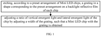
- the invention has the following beneficial effects: according to a preset arrangement of Mini LED chips, a grating in a shape corresponding to the preset arrangement is etched on a backlight reflective layer of each chip, such that the light shape of the Mini LED chips can be controlled; the shape of the grating corresponds to the preset arrangement of the chips, such that the chips can be divided into more regions, which is equivalent to increasing the arrangement density of the chips, the visual resolution experience is improved, and the resolution perceived by human eyes is increased, thus improving the display effect of the chips; and the width of the grating can be adjusted to change the ratio of vertical emergent light and lateral emergent light of the chip, so as to adjust the angle and intensity of emergent light of the chip, such that the control effect and display effect of the Mini LED chips are further improved.
- this embodiment of the invention provides a fabrication method for a backlight-type Mini LED chip, comprising the following steps:
- the invention has the following beneficial effects: according to a preset arrangement of Mini LED chips, a grating in a shape corresponding to the preset arrangement is etched on a backlight reflective layer of each chip, such that the light shape of the Mini LED chips can be controlled; the shape of the grating corresponds to the preset arrangement of the chips, such that the chips can be divided into more regions, which is equivalent to increasing the arrangement density of the chips, the visual resolution experience is improved, and the resolution perceived by human eyes is increased, thus improving the display effect of the chips; and the width of the grating can be adjusted to change the ratio of vertical emergent light and lateral emergent light of the chip, so as to adjust the angle and intensity of emergent light of the chip, such that the control effect and display effect of the Mini LED chips are further improved.
- the grating in the shape corresponding to the preset arrangement comprises:
- the grating is a cross line which is perpendicular to four edges of the chip and has an intersection point being the central point of the chip; or, the grating is a square grating with the central point of the chip as a center; if the preset arrangement is a rhombic matrix, the grating is two diagonal lines of the chip. In this way, the partition in the chips is kept horizontally consistent with the arrangement of the chips, and after the grating is etched, the visual resolution experience is improved, which is equivalent to improving the arrangement density of the chip, thus increasing the resolution visually perceived by human eyes.
- adjusting the ratio of vertical emergent light and lateral emergent light of the chip by adjusting the width of the grating comprises: Determining whether the lateral emergent light of the chip is more than the vertical emergent light of the chip; if so, increasing the width of the grating; otherwise, decreasing the width of the grating.
- the width of the grating when lateral emergent light of the chip is more than vertical emergent light of the chip, that is, when the brightness above the chip is relatively low, the width of the grating can be increased, which is especially suitable for high-density and high-resolution backlight; when lateral emergent light of the chip is less than vertical emergent light of the chip, the width of the grating of the chip can be decreased, such that the ratio of lateral light to vertical light is adjusted to make the overall emergent light uniform.
- etching according to a preset arrangement of Mini LED chips, a grating in a shape corresponding to the preset arrangement on a backlight reflective film of each chip comprises:
- the flip chip is machined at the end, away from the substrate layer, of the epitaxial wafer to improve the luminous efficiency of the chip; and accurate alignment of the wafer can be realized through the lithographic back alignment method, and grating lithography on the backlight reflective film can be realized through exposure, development, transfer of the gating pattern, metal evaporation of the backlight reflective film and stripping of metal at the position corresponding to the grating, and thus, the display efficiency is improved.
- the preset material sequence is sequentially nickel, silver, nickel, titanium-tungsten, nickel, and titanium-tungsten.
- metal evaporation is performed according to the sequence of nickel, silver, nickel, titanium-tungsten, nickel, and titanium-tungsten, and the grating is reflective, such that light attenuation of the chip will not be caused, thus improving the display efficiency.
- performing alignment on a photomask and an existing pattern of the fine polished wafer through a back alignment method comprises: Reserving a metal alignment pattern, which is seen from a back side of the wafer by reflection, on a front side of the wafer, and performing alignment on the photomask and the existing pattern of the wafer.
- the fabrication method comprises: Cutting the chip according to a preset interval, and arranging chips obtained after cutting according to the preset arrangement.
- the chip is cut according to a preset interval, chips obtained after cutting are arranged according to the preset arrangement, and gaps between the chips form lateral emergent regions, which can improve the display efficiency in conjunction with vertical emergent light of the chips.
- FIG. 2 another embodiment of the invention provides a backlight-type Mini LED chip, comprising a back light-shield reflective layer, a substrate layer, and a flip chip, wherein:
- a grating in a shape corresponding to the preset arrangement is etched on a backlight reflective layer of each chip, such that the light shape of the Mini LED chips can be controlled;
- the shape of the grating corresponds to the preset arrangement of the chips, such that the chips can be divided into more regions, which is equivalent to increasing the arrangement density of the chips, the visual resolution experience is improved, and the resolution perceived by human eyes is increased, thus improving the display effect of the chips;
- the width of the grating can be adjusted to change the ratio of vertical emergent light and lateral emergent light of the chip, so as to adjust the angle and intensity of emergent light of the chip, such that the control effect and display effect of the Mini LED chips are further improved.
- the preset arrangement of the Mini LED chips is a rectangular matrix or a rhombic matrix, and an interval between the Mini LED chips is 100 ⁇ m-15000 ⁇ m.
- the chip is cut according to a preset interval, chips obtained after cutting are arranged according to the preset arrangement, and gaps between the chips form lateral emergent regions, which can improve the display efficiency in conjunction with vertical emergent light of the chips.
- the grating is a cross line which is perpendicular to four edges of the chip and has an intersection point being the central point of the chip; or, the grating is a square grating with the central point of the chip as a center;
- the grating is a cross line which is perpendicular to four edges of the chip and has an intersection point being the central point of the chip; or, the grating is a square grating with the central point of the chip as a center; if the preset arrangement is a rhombic matrix, the grating is two diagonal lines of the chip. In this way, the partition in the chips is kept horizontally consistent with the arrangement of the chips, and after the grating is etched, the visual resolution experience is improved, which is equivalent to improving the arrangement density of the chip, thus increasing the resolution visually perceived by human eyes.
- a fabrication method for a backlight-type Mini LED chip comprises the following steps:
- the grating when the preset arrangement is a matrix, the grating is cross-shaped or square, so the partition in the chips is kept horizontally consistent with the arrangement of the chips, thus improving the visual resolution experience after partition; and with the increase of regions, the arrangement density of rectangular pixels is increased. Light can be emitted from gaps of the grating and two sides of the chip, so compared with chips without gratings, light can be emitted from more portions.
- the preset arrangement is rhombic
- the grating is X-shaped, which is consistent with the arrangement direction of the chips, so light can also be emitted from more portions; and original light-emitting regions are further divided, such that the arrangement density of rhombic pixels is increased.
- Such density increase effect is realized in one backlight chip;
- the size of an opening of the grating can be adjusted by controlling the design size of the photomask, so as to adjust the ratio of front emergent light and lateral emergent light of the chip, and thus, the shape, scope and intensity distribution of emergent light are adjusted, the chip arrangement on a substrate can be optimized, and the demand for optical elements such as a light guide plate and a diffuser plate on the substrate can be reduced.
- the light-emitting scope of the Mini LED array processed by the grating is further partitioned, so the resolution visually perceived by human eyes is better than that of chips without gratings.
- this embodiment provides a chip fabrication method in a case where the preset arrangement of Mini LED chips is a rectangular matrix, which comprises:
- this embodiment provides a chip fabrication method in a case where the preset arrangement of Mini LED chips is a rhombic matrix, which comprises:
- a backlight-type Mini LED chip comprises a back light-shield reflective layer, a substrate layer and a flip chip, wherein:
- the preset arrangement of the Mini LED chips is a rectangular matrix or a rhombic matrix, and an interval between the Mini LED chips is 100 ⁇ m-15000 ⁇ m.
- the grating is a cross line which is perpendicular to four edges of the chip and has an intersection point being the central point of the chip; or, the grating is a square grating with the central point of the chip as a center;
- a grating in a shape corresponding to the preset arrangement is etched on a backlight reflective layer of each chip, such that the light shape of the Mini LED chips can be controlled;
- the shape of the grating corresponds to the preset arrangement of the chips, such that the chips can be divided into more regions, which is equivalent to increasing the arrangement density of the chips, the visual resolution experience is improved, and the resolution perceived by human eyes is increased, thus improving the display effect of the chips;
- the width of the grating can be adjusted to change the ratio of vertical emergent light and lateral emergent light of the chip, so as to adjust the angle and intensity of emergent light of the chip, such that the control effect and display effect of the Mini LED chips are further improved.
- the size of an opening of the grating of the Mini LED chip can be adjusted by controlling the design size of the photomask, so as to adjust the ratio of front emergent light and lateral emergent light of the chip, and thus, the shape, scope and intensity distribution of emergent light are adjusted.
Landscapes
- Physics & Mathematics (AREA)
- Nonlinear Science (AREA)
- Mathematical Physics (AREA)
- Chemical & Material Sciences (AREA)
- Crystallography & Structural Chemistry (AREA)
- General Physics & Mathematics (AREA)
- Optics & Photonics (AREA)
- Led Devices (AREA)
Applications Claiming Priority (2)
| Application Number | Priority Date | Filing Date | Title |
|---|---|---|---|
| CN202110919850.1A CN113644058B (zh) | 2021-08-11 | 2021-08-11 | 一种背光型Mini LED芯片及其制造方法 |
| PCT/CN2021/114878 WO2023015617A1 (zh) | 2021-08-11 | 2021-08-27 | 一种背光型Mini LED芯片及其制造方法 |
Publications (2)
| Publication Number | Publication Date |
|---|---|
| EP4177948A1 true EP4177948A1 (de) | 2023-05-10 |
| EP4177948A4 EP4177948A4 (de) | 2024-07-10 |
Family
ID=78420923
Family Applications (1)
| Application Number | Title | Priority Date | Filing Date |
|---|---|---|---|
| EP21952106.9A Pending EP4177948A4 (de) | 2021-08-11 | 2021-08-27 | Mini-led-chip vom hintergrundbeleuchtungstyp und herstellungsverfahren dafür |
Country Status (4)
| Country | Link |
|---|---|
| US (1) | US20230136566A1 (de) |
| EP (1) | EP4177948A4 (de) |
| CN (1) | CN113644058B (de) |
| WO (1) | WO2023015617A1 (de) |
Families Citing this family (2)
| Publication number | Priority date | Publication date | Assignee | Title |
|---|---|---|---|---|
| EP4293734B1 (de) * | 2022-04-29 | 2026-02-18 | Fujian Prima Optoelectronics Co., Ltd | Mikro-led-lichtprojektionschip und verfahren zur herstellung davon |
| US12538620B2 (en) * | 2022-05-27 | 2026-01-27 | BOE MLED Technology Co., Ltd. | Light emitting substrate, method for manufacturing thereof, and display apparatus |
Family Cites Families (15)
| Publication number | Priority date | Publication date | Assignee | Title |
|---|---|---|---|---|
| AU2002217845A1 (en) * | 2000-11-16 | 2002-05-27 | Emcore Corporation | Microelectronic package having improved light extraction |
| US7808011B2 (en) * | 2004-03-19 | 2010-10-05 | Koninklijke Philips Electronics N.V. | Semiconductor light emitting devices including in-plane light emitting layers |
| KR101301445B1 (ko) * | 2008-12-30 | 2013-08-28 | 엘지디스플레이 주식회사 | 발광 다이오드 모듈 및 이를 구비한 백라이트 어셈블리 |
| CN101572286B (zh) * | 2009-05-27 | 2011-12-21 | 苏州大学 | 偏振出光发光二极管 |
| US20120112218A1 (en) * | 2010-11-04 | 2012-05-10 | Agency For Science, Technology And Research | Light Emitting Diode with Polarized Light Emission |
| WO2014108782A1 (en) * | 2013-01-09 | 2014-07-17 | Koninklijke Philips N.V. | Shaped cavity in substrate of a chip scale package led |
| CN103094427A (zh) * | 2013-01-28 | 2013-05-08 | 华中科技大学 | 一种利用双面图形化衬底提高AlGaN基UV-LED发光效率方法 |
| CN103337576A (zh) * | 2013-06-09 | 2013-10-02 | 武汉迪源光电科技有限公司 | 图形化衬底及其制造方法、led芯片及其制造方法 |
| CN104269480B (zh) * | 2014-10-22 | 2017-06-16 | 湘能华磊光电股份有限公司 | 一种led倒装芯片及其制作方法 |
| TWI614887B (zh) * | 2016-02-26 | 2018-02-11 | 趨勢照明股份有限公司 | 具有點陣式發光二極體光源的晶圓級微型顯示器及其製造方法 |
| WO2017171812A1 (en) * | 2016-03-31 | 2017-10-05 | Intel Corporation | Micro light emitting diode |
| KR102560709B1 (ko) * | 2016-08-30 | 2023-07-27 | 삼성전자주식회사 | 지향성 백라이트 유닛, 이를 포함한 입체 영상 표시 장치 |
| CN110676358B (zh) * | 2019-11-04 | 2025-01-14 | 佛山市国星半导体技术有限公司 | 一种高亮度正装led芯片及其制作方法 |
| CN111624817B (zh) * | 2020-06-30 | 2023-01-13 | 京东方科技集团股份有限公司 | 背光模组及其制造方法、显示装置 |
| CN112882287A (zh) * | 2021-01-15 | 2021-06-01 | 北海惠科光电技术有限公司 | 一种背光模组和显示设备 |
-
2021
- 2021-08-11 CN CN202110919850.1A patent/CN113644058B/zh active Active
- 2021-08-27 WO PCT/CN2021/114878 patent/WO2023015617A1/zh not_active Ceased
- 2021-08-27 EP EP21952106.9A patent/EP4177948A4/de active Pending
-
2022
- 2022-12-30 US US18/091,487 patent/US20230136566A1/en not_active Abandoned
Also Published As
| Publication number | Publication date |
|---|---|
| US20230136566A1 (en) | 2023-05-04 |
| EP4177948A4 (de) | 2024-07-10 |
| WO2023015617A1 (zh) | 2023-02-16 |
| CN113644058A (zh) | 2021-11-12 |
| CN113644058B (zh) | 2022-06-28 |
Similar Documents
| Publication | Publication Date | Title |
|---|---|---|
| US6984927B2 (en) | Display unit | |
| US20230136566A1 (en) | Backlight-type mini led chip and fabrication method therefor | |
| JP7604471B2 (ja) | 照射装置を製造する方法 | |
| US11994766B2 (en) | Backlight module, method of manufacturing the same, display device | |
| US12295193B2 (en) | Display substrate and display device | |
| EP2980638B1 (de) | Farbige flüssigkristallanzeige mit zusätzlichen weissen pixeln | |
| US11766744B2 (en) | Method of forming a plurality of gratings | |
| US10310321B2 (en) | Optical element, manufacturing method of optical element, and optical device | |
| KR20200096529A (ko) | 발광 적층 구조체를 갖는 디스플레이 장치 | |
| JP2008191668A (ja) | フォトレジストの形成方法及び表示パネルの製造方法 | |
| TW202327141A (zh) | 含超材料光準直特徵之發光二極體陣列及形成彼之方法 | |
| JP2020532823A (ja) | 格子を含む光導波路 | |
| WO2019000987A1 (zh) | 背光源及其制造方法、显示装置 | |
| US10840418B1 (en) | Fabricating parabolic-shaped LEDs | |
| US20220100078A1 (en) | Devices and methods for variable etch depths | |
| CN112698526A (zh) | 一种液晶显示面板和液晶显示器 | |
| US20240282896A1 (en) | Light-emitting unit | |
| KR20250116747A (ko) | 비균일 두께의 박막 층들을 갖는 회절 광학 요소를 생성하는 방법, 및 회절 광학 요소 박막 층들을 갖는 조명 광 가이드 | |
| CN211264026U (zh) | 一种液晶显示模组和液晶显示装置 | |
| TWI912747B (zh) | 彩色濾光片基板及顯示裝置 | |
| TWI847938B (zh) | 發光單元 | |
| US20250366276A1 (en) | Light-emitting unit and light-emitting device including the same | |
| CN121620041A (zh) | 发光芯片及其制作方法 | |
| WO2026021192A1 (zh) | 导光板、背光模组、显示面板、导光板模具及其制作方法 | |
| CN116799127A (zh) | 量子点光转换板及其制作方法、显示装置 |
Legal Events
| Date | Code | Title | Description |
|---|---|---|---|
| STAA | Information on the status of an ep patent application or granted ep patent |
Free format text: STATUS: UNKNOWN |
|
| STAA | Information on the status of an ep patent application or granted ep patent |
Free format text: STATUS: THE INTERNATIONAL PUBLICATION HAS BEEN MADE |
|
| PUAI | Public reference made under article 153(3) epc to a published international application that has entered the european phase |
Free format text: ORIGINAL CODE: 0009012 |
|
| STAA | Information on the status of an ep patent application or granted ep patent |
Free format text: STATUS: REQUEST FOR EXAMINATION WAS MADE |
|
| 17P | Request for examination filed |
Effective date: 20230206 |
|
| AK | Designated contracting states |
Kind code of ref document: A1 Designated state(s): AL AT BE BG CH CY CZ DE DK EE ES FI FR GB GR HR HU IE IS IT LI LT LU LV MC MK MT NL NO PL PT RO RS SE SI SK SM TR |
|
| REG | Reference to a national code |
Ref country code: DE Ref legal event code: R079 Free format text: PREVIOUS MAIN CLASS: H01L0025075000 Ipc: H01L0033000000 |
|
| A4 | Supplementary search report drawn up and despatched |
Effective date: 20240611 |
|
| RIC1 | Information provided on ipc code assigned before grant |
Ipc: H01L 33/46 20100101ALI20240605BHEP Ipc: H01L 33/00 20100101AFI20240605BHEP |
|
| DAV | Request for validation of the european patent (deleted) | ||
| DAX | Request for extension of the european patent (deleted) | ||
| REG | Reference to a national code |
Ref country code: DE Ref legal event code: R079 Free format text: PREVIOUS MAIN CLASS: H01L0033000000 Ipc: H10H0029240000 |