EP4174927A1 - Wiring substrate and electronic device - Google Patents
Wiring substrate and electronic device Download PDFInfo
- Publication number
- EP4174927A1 EP4174927A1 EP21834285.5A EP21834285A EP4174927A1 EP 4174927 A1 EP4174927 A1 EP 4174927A1 EP 21834285 A EP21834285 A EP 21834285A EP 4174927 A1 EP4174927 A1 EP 4174927A1
- Authority
- EP
- European Patent Office
- Prior art keywords
- lead terminal
- lead
- wiring substrate
- plan
- view
- Prior art date
- Legal status (The legal status is an assumption and is not a legal conclusion. Google has not performed a legal analysis and makes no representation as to the accuracy of the status listed.)
- Withdrawn
Links
Images






Classifications
-
- H—ELECTRICITY
- H10—SEMICONDUCTOR DEVICES; ELECTRIC SOLID-STATE DEVICES NOT OTHERWISE PROVIDED FOR
- H10W—GENERIC PACKAGES, INTERCONNECTIONS, CONNECTORS OR OTHER CONSTRUCTIONAL DETAILS OF DEVICES COVERED BY CLASS H10
- H10W76/00—Containers; Fillings or auxiliary members therefor; Seals
- H10W76/10—Containers or parts thereof
- H10W76/12—Containers or parts thereof characterised by their shape
- H10W76/15—Containers comprising an insulating or insulated base
- H10W76/157—Containers comprising an insulating or insulated base having interconnections parallel to the insulating or insulated base
-
- H—ELECTRICITY
- H01—ELECTRIC ELEMENTS
- H01S—DEVICES USING THE PROCESS OF LIGHT AMPLIFICATION BY STIMULATED EMISSION OF RADIATION [LASER] TO AMPLIFY OR GENERATE LIGHT; DEVICES USING STIMULATED EMISSION OF ELECTROMAGNETIC RADIATION IN WAVE RANGES OTHER THAN OPTICAL
- H01S5/00—Semiconductor lasers
- H01S5/02—Structural details or components not essential to laser action
- H01S5/022—Mountings; Housings
- H01S5/023—Mount members, e.g. sub-mount members
-
- H—ELECTRICITY
- H05—ELECTRIC TECHNIQUES NOT OTHERWISE PROVIDED FOR
- H05K—PRINTED CIRCUITS; CASINGS OR CONSTRUCTIONAL DETAILS OF ELECTRIC APPARATUS; MANUFACTURE OF ASSEMBLAGES OF ELECTRICAL COMPONENTS
- H05K1/00—Printed circuits
- H05K1/02—Details
- H05K1/0213—Electrical arrangements not otherwise provided for
- H05K1/0216—Reduction of cross-talk, noise or electromagnetic interference
- H05K1/0218—Reduction of cross-talk, noise or electromagnetic interference by printed shielding conductors, ground planes or power plane
- H05K1/0219—Printed shielding conductors for shielding around or between signal conductors, e.g. coplanar or coaxial printed shielding conductors
-
- H—ELECTRICITY
- H05—ELECTRIC TECHNIQUES NOT OTHERWISE PROVIDED FOR
- H05K—PRINTED CIRCUITS; CASINGS OR CONSTRUCTIONAL DETAILS OF ELECTRIC APPARATUS; MANUFACTURE OF ASSEMBLAGES OF ELECTRICAL COMPONENTS
- H05K1/00—Printed circuits
- H05K1/02—Details
- H05K1/0213—Electrical arrangements not otherwise provided for
- H05K1/0237—High frequency adaptations
- H05K1/0245—Lay-out of balanced signal pairs, e.g. differential lines or twisted lines
-
- H—ELECTRICITY
- H10—SEMICONDUCTOR DEVICES; ELECTRIC SOLID-STATE DEVICES NOT OTHERWISE PROVIDED FOR
- H10F—INORGANIC SEMICONDUCTOR DEVICES SENSITIVE TO INFRARED RADIATION, LIGHT, ELECTROMAGNETIC RADIATION OF SHORTER WAVELENGTH OR CORPUSCULAR RADIATION
- H10F77/00—Constructional details of devices covered by this subclass
- H10F77/93—Interconnections
- H10F77/933—Interconnections for devices having potential barriers
-
- H—ELECTRICITY
- H10—SEMICONDUCTOR DEVICES; ELECTRIC SOLID-STATE DEVICES NOT OTHERWISE PROVIDED FOR
- H10W—GENERIC PACKAGES, INTERCONNECTIONS, CONNECTORS OR OTHER CONSTRUCTIONAL DETAILS OF DEVICES COVERED BY CLASS H10
- H10W76/00—Containers; Fillings or auxiliary members therefor; Seals
- H10W76/60—Seals
-
- H—ELECTRICITY
- H05—ELECTRIC TECHNIQUES NOT OTHERWISE PROVIDED FOR
- H05K—PRINTED CIRCUITS; CASINGS OR CONSTRUCTIONAL DETAILS OF ELECTRIC APPARATUS; MANUFACTURE OF ASSEMBLAGES OF ELECTRICAL COMPONENTS
- H05K1/00—Printed circuits
- H05K1/02—Details
- H05K1/03—Use of materials for the substrate
- H05K1/0306—Inorganic insulating substrates, e.g. ceramic, glass
-
- H—ELECTRICITY
- H05—ELECTRIC TECHNIQUES NOT OTHERWISE PROVIDED FOR
- H05K—PRINTED CIRCUITS; CASINGS OR CONSTRUCTIONAL DETAILS OF ELECTRIC APPARATUS; MANUFACTURE OF ASSEMBLAGES OF ELECTRICAL COMPONENTS
- H05K2201/00—Indexing scheme relating to printed circuits covered by H05K1/00
- H05K2201/10—Details of components or other objects attached to or integrated in a printed circuit board
- H05K2201/10227—Other objects, e.g. metallic pieces
- H05K2201/1034—Edge terminals, i.e. separate pieces of metal attached to the edge of the printed circuit board [PCB]
-
- H—ELECTRICITY
- H05—ELECTRIC TECHNIQUES NOT OTHERWISE PROVIDED FOR
- H05K—PRINTED CIRCUITS; CASINGS OR CONSTRUCTIONAL DETAILS OF ELECTRIC APPARATUS; MANUFACTURE OF ASSEMBLAGES OF ELECTRICAL COMPONENTS
- H05K3/00—Apparatus or processes for manufacturing printed circuits
- H05K3/30—Assembling printed circuits with electric components, e.g. with resistors
- H05K3/32—Assembling printed circuits with electric components, e.g. with resistors electrically connecting electric components or wires to printed circuits
- H05K3/34—Assembling printed circuits with electric components, e.g. with resistors electrically connecting electric components or wires to printed circuits by soldering
- H05K3/3405—Edge mounted components, e.g. terminals
-
- H—ELECTRICITY
- H10—SEMICONDUCTOR DEVICES; ELECTRIC SOLID-STATE DEVICES NOT OTHERWISE PROVIDED FOR
- H10F—INORGANIC SEMICONDUCTOR DEVICES SENSITIVE TO INFRARED RADIATION, LIGHT, ELECTROMAGNETIC RADIATION OF SHORTER WAVELENGTH OR CORPUSCULAR RADIATION
- H10F77/00—Constructional details of devices covered by this subclass
- H10F77/50—Encapsulations or containers
-
- H—ELECTRICITY
- H10—SEMICONDUCTOR DEVICES; ELECTRIC SOLID-STATE DEVICES NOT OTHERWISE PROVIDED FOR
- H10W—GENERIC PACKAGES, INTERCONNECTIONS, CONNECTORS OR OTHER CONSTRUCTIONAL DETAILS OF DEVICES COVERED BY CLASS H10
- H10W44/00—Electrical arrangements for controlling or matching impedance
- H10W44/20—Electrical arrangements for controlling or matching impedance at high-frequency [HF] or radio frequency [RF]
-
- H—ELECTRICITY
- H10—SEMICONDUCTOR DEVICES; ELECTRIC SOLID-STATE DEVICES NOT OTHERWISE PROVIDED FOR
- H10W—GENERIC PACKAGES, INTERCONNECTIONS, CONNECTORS OR OTHER CONSTRUCTIONAL DETAILS OF DEVICES COVERED BY CLASS H10
- H10W90/00—Package configurations
- H10W90/701—Package configurations characterised by the relative positions of pads or connectors relative to package parts
Definitions
- the present disclosure relates to a wiring substrate and an electronic device.
- Patent Literature 1 there is described a package for housing a high-frequency semiconductor device employing differential signaling as a transmission method.
- This package includes: a ceramic substrate; ground line conductors extending at right angles from the edge end of at least one side of the outer peripheral part of the lower surface of the ceramic substrate; and differential signal line conductors each composed of a pair of line conductors extending parallel to the ground line conductors and sandwiched between the ground line conductors on both sides.
- Patent Literature 1 JP 2016-146439 A
- the present disclosure relates to a wiring substrate and an electronic device having improved high-frequency properties.
- a wiring substrate according to the present disclosure includes:
- An electronic device includes:
- a wiring substrate having improved high-frequency properties can be provided. Further, according to the present disclosure, an electronic device having excellent high-frequency properties can be provided.
- a wiring substrate 10A of a first embodiment is a wiring substrate where an electronic component is to be mounted.
- the electronic component may be an electronic component that is driven at high frequency or an electronic component to and from which high-frequency signals are input and output.
- the wiring substrate 10A includes a substrate 1 having a first surface S1, ground conductors 2 located on the first surface S1, and signal conductors 3 located on the first surface S1.
- the substrate 1 has a rectangular plate-like bottom 1a, and the lower surface of the bottom 1a constitutes the first surface S1.
- the substrate 1 also has a frame 1b located on the upper surface of the bottom 1a along the outer periphery of the bottom 1a.
- the upper surface of the bottom 1a and the inner surface of the frame 1b form a cavity.
- the upper surface of the bottom 1a is a mounting surface having a mounting part 5 where an electronic component is to be mounted.
- the substrate 1 further has a through hole 6 in a part of the frame 1b.
- the wiring substrate 10A has a seal ring 4 on the upper surface of the frame 1b of the substrate 1.
- the substrate 1 is composed of a plurality of insulating substrates stacked on top of one another in the thickness direction, for example.
- a ceramic material such as an aluminum oxide sintered body, a mullite sintered body, a silicon carbide sintered body, an aluminum nitride sintered body or a silicon nitride sintered body, or a glass ceramic material can be used.
- the seal ring 4 is used as a seal material for airtight sealing with a lid after an electronic component is mounted on the mounting part 5.
- the seal ring 4 is configured, for example, such that a frame-shaped conductor made of conducive paste containing a high-melting-point metal, such as tungsten or molybdenum, is brazed and joined (bonded) to a frame-shaped metal plate made of an Fe-Ni-based alloy or an Fe-Ni-Co-based alloy with a brazing material or the like.
- a frame-shaped conductor made of conducive paste containing a high-melting-point metal such as tungsten or molybdenum
- the first surface S1 of the substrate 1 is, for example, rectangular, and has two long sides parallel to X direction and two short sides parallel to Y direction.
- the ground conductors 2 and the signal conductors 3 are arranged along one short side of the first surface S1 such that one ground conductor 2 alternates with two signal conductors 3, and at each end, a ground conductor 2 is present.
- a ground conductor 2 and a signal conductor 3 adjacent to one another and signal conductors 3 adjacent to one another are arranged so as to be insulated from one another.
- the ground conductors 2 and the signal conductors 3 on the first surface S1 is, for example, rectangular and may have a predetermined width and a predetermined length inward from the edge of the short side of the first surface S1.
- the ground conductors 2 may be U-shaped so as to surround the signal conductors 3.
- the "U-shaped" is, in other words, a shape formed by ends of two ground conductors 2 connected by a metallic object. Areas of the ground conductors 2 and the signal conductors 3 on the first surface S1 and spaces between the adjacent ground conductor 2 and signal conductor 3 and between the adjacent signal conductors 3 thereon are appropriately determined on the basis of design of an electronic device to which the wiring substrate 10A is applied.
- the ground conductors 2 and the signal conductors 3 contain a metal material, such as gold, silver, copper, nickel, tungsten, molybdenum or manganese.
- the ground conductors 2 and the signal conductors 3 may be formed on the first surface S1 by co-firing with the substrate 1 in the form of a metallized layer(s), a plating layer(s) or the like or by metal plating.
- the ground conductors 2 and the signal conductors 3 may have a substantially uniform thickness throughout, which may be about 5 to 30 ⁇ m.
- the ground conductors 2 and the signal conductors 3 may be surrounded by a coating member 7.
- the joining material is stemmed at boundaries between (i) the ground conductors 2 and the signal conductors 3 and (ii) the coating member 7. This can reduce spread of the joining material on the first surface S1, and this reduction of spread of the joining material reduces change in inductance due to spread of the joining material, so that the wiring substrate 10A is impedance-matched.
- the reduction of spread of the joining material also results in forming a moderate fillet of the joining material, so that joining strength (bonding) of the ground conductors 2 and the first lead terminals and joining (bonding) strength of the signal conductors 3 and the second lead terminals increase.
- the shape of the coating member 7 is not limited to the above.
- the coating member 7 may be arranged so as to surround each ground conductor 2 and also surround two adjacent signal conductors 3 collectively.
- reduction of spread of the joining material results in forming a moderate fillet of the joining material, so that joining strength of the ground conductors 2 and the first lead terminals and joining strength of the signal conductors 3 and the second lead terminals increase.
- the shape of the coating member so as to surround two adjacent signal conductors 3 collectively can also achieve miniaturization of the wiring substrate 10A in addition to increase in the joining strength.
- a ceramic material such as an aluminum oxide sintered body, a chromium sintered body, a mullite sintered body, a silicon carbide sintered body, an aluminum nitride sintered body or a silicon nitride sintered body, or a glass ceramic material can be used.
- the wiring substrate 10A has first lead terminals 20A that are in contact with the respective ground conductors 2 and second lead terminals 30 that are aligned with the first lead terminals 20A and in contact with the respective signal conductors 3.
- the first lead terminals 20A and the second lead terminals 30 extend at right angles to, of the first surface S1, the short side(s) that is parallel to the Y direction, namely extend parallel to the X direction.
- the first lead terminals 20A and the second lead terminals 30 are, for example, connected to outside, so that an electronic component mounted on the mounting part 5 of the substrate 1 outputs and receives electric signals to and from the outside.
- the bottom 1a of the substrate 1 is, for example, mainly composed of an insulating substrate(s), and has a wiring conductor(s), a through conductor(s) and/or the like therein so that an electronic component or its peripheral components on the mounting part 5 of the upper surface are electrically connected to the ground conductors 2 and the signal conductors 3 on the lower surface.
- This allows an electronic component mounted on the mounting part 5 to output and receive electric signals to and from the outside via the first lead terminals 20A and the second lead terminals 30 that are respectively in contact with the ground conductors 2 and the signal conductors 3.
- the first lead terminals 20A and the second lead terminals 30 are made of a metal material, and for example, after molded into the shapes described below, respectively joined to the ground conductors 2 and the signal conductors 3 with a joining material, such as a brazing material.
- the material of the first lead terminals 20A and the second lead terminals 30 may be a metal, such as copper, iron, nickel, cobalt or chromium, or a metallic alloy containing such a metal, for example.
- Each first lead terminal 20A has a first end 21 at a position on the substrate 1 in plan perspective view toward the first surface S1 and a second end 22 not on the substrate 1 but at a position on an extension from the first end 21 in parallel to the X direction.
- the first lead terminal 20A has a contacting part 23, a connecting part 26 and a lead part 27 in this order from the first end 21 to the second end 22.
- the first lead terminal 20A has a second surface S2 facing the first surface S1 and a third surface S3 opposite the second surface S2.
- the first lead terminal 20A may be a long, narrow plate having predetermined width, length and thickness, for example. In this embodiment, the first lead terminal 20A has a substantially uniform thickness along the length direction.
- the width direction, length direction and thickness direction of the first lead terminal 20A are a direction parallel to the Y direction, a direction parallel to the X direction and a direction parallel to the Z direction, respectively.
- the contacting part 23 is a part that includes the first end 21 and at which the second surface S2 contacts the ground conductor 2.
- the connecting part 26 is a part that includes a first bend 24 at a positon away from the first end 21 across the contacting part 23 and a second bend 25 at a position closer to the second end 22 than the first bend 24.
- the first bend 24 is where the second surface S2 separates from the ground conductor 2. More specifically, the contacting part 23 is a part from the first end 21 to the first bend 24, and the connecting part 26 is a part from the first bend 24 to the second bend 25.
- the lead part 27 is a part connected to the second bend 25 and extending to the second end 22.
- the first bend 24 is where the first lead terminal 20A is bent in the -Z direction, namely downward, so as to separate from the ground conductor 2.
- the second bend 25 is where the first lead terminal 20A is bent in the +Z direction, namely upward, with respect to the bending direction at the first bend 24.
- the entire first lead terminal 20A is bent at the first bend 24 and the second bend 25, but like a first lead terminal (s) 20F described below, only the second surface S2 may be bent at the first bend 24 and the second bend 25. That is, in a wiring substrate of an embodiment, at least the second surface of each first lead terminal has a first bend and a second bend.
- the first lead terminal 20A having the first bend 24, the second bend 25 or both can absorb, with the first bend 24 or the second bend 25, pressure applied to the first lead terminal 20A when an external board is connected to the wiring substrate 10A. This can reduce occurrence of damage to the first lead terminal 20A.
- the second surface S2 of the first lead terminal 20A is, for example, a surface parallel to the first surface S1 at the contacting part 23, a surface having a predetermined angle to the first surface S1 at the connecting part 26, and a surface parallel to the first surface S1 at the lead part 27.
- an angle formed by the second surface S2 at the connecting part 26 and a plane obtained by extending the second surface S2 at the contacting part 23 is represented by " ⁇ 1".
- the angle ⁇ 1 may range from 20 to 60 degrees, for example.
- an angle formed by the second surface S2 at the connecting part 26 and the second surface S2 at the lead part 27 is represented by " ⁇ 1".
- the angle ⁇ 1 is expressed by "180 - ⁇ 1".
- the third surface S3 may have the same shape as the second surface S2, for example.
- an angle formed by the third surface S3 at the contacting part 23 and the third surface S3 at the connecting part 26 is represented by " ⁇ 2”
- an angle formed by the third surface S3 at the connecting part 26 and a plane obtained by extending the third surface S3 at the lead part 27 is represented by " ⁇ 2”
- “Angle ⁇ 2 ⁇ Angle ⁇ 1” and "Angle ⁇ 2 ⁇ Angle ⁇ 1” may hold.
- the lead part 27 is, for example, a part that is connected to an external board, such as a flexible board, such that the third surface S3 at the lead part 27 contacts the upper surface of the external board.
- the connecting part 26 is a part that is not in contact with either the ground conductor 2 or an external board and is located in a region in mid-air.
- Distance H between the plane obtained by extending the second surface S2 of the first lead terminal 20A at the contacting part 23 and the second surface S2 thereof at the lead part 27 may be about 0.1 to 0.5 mm.
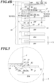
- the connecting part 26 When the first lead terminal 20A is viewed in the XY plane, which is parallel to the first surface S1, the connecting part 26 has a part having a shorter distance D1 to the second lead terminal(s) 30 than the contacting part 23 ( FIG. 4A ). More specifically, the connecting part 26 is composed of a first tapered part 26a, a second tapered part 26c and an interconnecting part 26b.
- the first tapered part 26a is a part where a width W1 increases toward the second end 22.
- the second tapered part 26b is a part that is located closer to the second end 22 than the first tapered part 26a and where the width W1 decreases toward (to) the lead part 27.
- the interconnecting part 26c is a part that is located between the first tapered part 26a and the second tapered part 26c.
- the first tapered part 26a is a region from the first bend 24 to its boundary with the interconnecting part 26b
- the second tapered part 26c is a region from its boundary with the interconnecting part 26b to the second bend 25.
- each first lead terminal 20A is interposed between two second lead terminals 30.
- the first lead terminal 20A has the width W1 that gradually increases at the first tapered part 26a such that the sides extending in the length direction (X direction) are spread in the width direction (Y direction) until they reach the interconnecting part 26b.
- the first lead terminal 20A has the width W1 that is kept unchanged at the interconnecting part 26b from the first end 21 toward the second end 22. That is, the width W1 at the interconnecting part 26b is uniform. This makes it possible to stably adjust impedance.
- the first lead terminal 20A has the width W1 that gradually decreases at the second tapered part 26c such that the sides extending in the length direction (X direction) get closer in the width direction (Y direction).
- the sides of the first lead terminal 20A extending in the length direction are substantially symmetrical about a center line that connects the center of the first end 21 and the center of the second end 22.
- the width W1 at the first tapered part 26a may gradually increase from the first end 21 toward the second end 22 at a predetermined rate
- the width W1 at the second tapered part 26c may gradually decrease from the first end 21 toward the second end 22 at a predetermined rate. This can gradually change impedance at the signal conductor 3 and the second lead terminal 30 that are adjacent to the first lead terminal 20A and hence makes impedance adjustment easy.
- the dimension in the length direction of the second lead terminals 30 may be the same as that of the first lead terminals 20A. That is, the second lead terminals 30 and the first lead terminals 20A may have the same length.
- the second lead terminals 30 are parallel to the first lead terminals 20A.
- Each second lead terminal 30 has a predetermined narrow width W2 that is set, for example, in conformity with desired high-frequency properties and strength. In order to transmit high-frequency signals, the second lead terminal 30 is formed such that the width W2 does not greatly change.
- a first lead terminal 20A and two second lead terminals 30 between which the first lead terminal 20A is interposed having their respective configurations described above allow the first lead terminal 20A to have, at the interconnecting part 26b of the connecting part 26, the shortest distance D1 to each of the second lead terminals 30 located on both sides.
- the distance D1 between a first lead terminal 20A and a second lead terminal 30 located on one side of the first lead terminal 20A is the same as the distance D1 between the first lead terminal 20A and a second lead terminal 30 located on the other side thereof.
- the distance D1 may be about 0.2 to 1.0 mm, for example.
- the first lead terminal 20A having, in the connecting part 26 located in mid-air, a part having a short distance D1 to each of the second lead terminals 30 makes impedance matching easy.
- the wiring substrate 10A is excellent in high-frequency properties.
- the first lead terminal 20A having a wide width W1 at the connecting part 26 can have a large volume. This reduces occurrence of crosstalk.
- the wiring substrate 10A is excellent in high-frequency properties.
- the first lead terminal 20A including the connecting part 26 having the first tapered part 26a, the interconnecting part 26b and the second tapered part 26c has the following advantages.
- the first lead terminal 20A having the first tapered part 26a and the second tapered part 26c is easy to process. That is, the first lead terminal 20A has higher workability than that having a corner(s) of an exterior angle of less than 90 degrees at a point(s) at/from which the width W1 changes.
- the first lead terminal 20A having the first tapered part 26a and the second tapered part 26c has less stress concentration at a point(s) at/from which the width W1 changes than that having a corner(s) of an exterior angle of, for example, 90 degrees at a point(s) at/from which the width W1 changes. This can reduce, in the first lead terminal 20A, appearance of cracks or the like due to pressure or the like from the outside.
- the width W1 of the first lead terminal 20A at the lead part 27 is determined by design of an external board, for example. If the set width W1 at the lead part 27 is narrow, it is, for the reasons described above, advantageous to the first lead terminal 20A to have the second tapered part 26c.
- the interconnecting part 26b is the part where the width W1 becomes the largest. In order to increase the volume of the first lead terminal 20A and increase the area of the part where the distance D1 between the first lead terminal 20A and the second lead terminal 30 becomes the shortest, it is advantageous to the interconnecting part 26b to have a longer length.
- the ratio of the lengths of the first tapered part 26a, the interconnecting part 26b and the second tapered part 26c of the first lead terminal 20A can be appropriately selected with a balance between workability and volume increase taken into account.
- the first tapered part 26a and the interconnecting part 26b lie on the substrate 1 in plan perspective view toward the first surface S1.
- the first tapered part 26a that is located inside of the outer periphery of the substrate 1 and bent can increase, in mid-air, the area of the part having a short distance D1 between the first lead terminal 20A and the second lead terminal 30. In mid-air, what surrounds the first lead terminal 20A is air having a lower dielectric constant than the substrate 1.
- the distance D1 between the first lead terminal 20A and the second lead terminal 30 being short makes impedance adjustment of the first lead terminal 20A and the second lead terminal 30 easy.
- Each second lead terminal 30 has a first end 31 and a second end 32.
- the first end 31 is at a position on the substrate 1 in plan perspective view toward the first surface S1.
- the second end 32 is not on the substrate 1 but at a position on an extension from the first end 31 in parallel to the X direction.
- the second lead terminal 30 has a contacting part 33, a connecting part 36 and a lead part 37 in this order from the first end 31 to the second end 32.
- the second lead terminal 30 has a fourth surface facing the first surface S1 and a fifth surface opposite the fourth surface.
- the second lead terminal 30 may be a long, narrow plate having predetermined width, length and thickness, for example. In this embodiment, the second lead terminal 30 has a substantially uniform thickness along the length direction, like the first lead terminal 20A.
- the width direction, length direction and thickness direction of the second lead terminal 30 may coincide with the width direction, length direction and thickness direction of the first lead terminal 20A, respectively. More specifically, the width direction, length direction and thickness direction of the second lead terminal 30 are a direction parallel to the Y direction, a direction parallel to the X direction and a direction parallel to the Z direction, respectively.
- Width 126b > Width W121 > Width W122 may hold. That is, “Difference between Width W126b and Width W121 > Difference between Width W126b and Width W122" may hold. In this case, stable impedance adjustment and package miniaturization can be achieved appropriately.
- the length (dimension in the length direction) L1 of the first lead terminal 20A may have the following relationship at the connecting part 26.
- L126a length at the first tapered part 26a
- L126c length at the second tapered part 26c
- L126a ⁇ L126c length at the second tapered part 26c
- the contacting part 33 of the second lead terminal 30 is a part that includes the first end 31 and at which the fourth surface contacts the signal conductor 3.
- the connecting part 36 of the second lead terminal 30 is a part that includes a first bend 34 at a position away from the first end 31 across the contacting part 33 and a second bend 35 at a position closer to the second end 32 than the first bend 34.
- the first bend 34 is where the fourth surface separates from the signal conductor 3. More specifically, the contacting part 33 of the second lead terminal 30 is a part from the first end 31 to the first bend 34, and the connecting part 36 of the second lead terminal 30 is a part from the first bend 34 to the second bend 35.
- the lead part 37 of the second lead terminal 30 is a part connected to the second bend 35 and extending to the second end 32.
- the second lead terminal 30 may have the same lateral shape as the first lead terminal 20A, for example.
- the first bend 34 is where the second lead terminal 30 is bent in the -Z direction, namely downward, so as to separate from the signal conductor 3
- the second bend 35 is where the second lead terminal 30 is bent in the +Z direction, namely upward, with respect to the bending direction at the first bend 34.
- the second lead terminal 30 having the first bend 34, the second bend 35 or both can reduce, with the first bend 34 or the second bend 35, pressure applied to the second lead terminal 30 when an external board is connected to the wiring substrate 10A. This can reduce occurrence of damage to the second lead terminal 30.
- the fourth surface of the second lead terminal 30 is, for example, a surface parallel to the first surface S1 at the contacting part 33, a surface having a predetermined angle to the first surface S1 at the connecting part 36, and a surface parallel to the first surface S1 at the lead part 37.
- An angle formed by the fourth surface at the connecting part 36 and a plane obtained by extending the fourth surface at the contacting part 33 may be in the same range as the angle ⁇ 1.
- an angle formed by the fourth surface at the connecting part 36 and the fourth surface at the lead part 37 may be in the same range as the angle ⁇ 1.
- the entire second lead terminal 30 is bent at the first bend 34 and the second bend 35.
- the fifth surface may have the same shape as the fourth surface.
- the lead part 37 of the second lead terminal 30 is, for example, a part that is connected to an external board, such as a flexible board, such that the fifth surface at the lead part 37 contacts the upper surface of the external board.
- the fifth surface of the second lead terminal 30 at the lead part 37 is usually on the same plane as the third surface S3 of the first lead terminal 20A at the lead part 27.
- the connecting part 36 is a part that is not in contact with either the signal conductor 3 or an external board and is located in a region in mid-air.
- the width W2 of the second lead terminal 30 may be uniform at the contacting part 33, the connecting part 36 and the lead part 37 ( FIG. 4A ).
- distance D2 between two second lead terminals 30 adjacent to one another is kept uniform from the first end(s) 31 to the second end(s) 32 of the second lead terminal(s) 30.
- the distance D1 between a second lead terminal 30 and a first lead terminal 20A adjacent to one another becomes the shortest at the interconnecting part 26b of the connecting part 26 of the first lead terminal 20A.
- FIG. 4B is an enlarged view of first lead terminals, second lead terminals and their surroundings in a wiring substrate 10A' as a modification of the wiring substrate 10A of the first embodiment.
- the wiring substrate 10A' is configured in the same manner as the wiring substrate 10A of the first embodiment except that the second lead terminals 30 in the wiring substrate 10A of the first embodiment are replaced by second lead terminals 30V.
- the second lead terminals 30V which are different from the second lead terminals 30, are mainly described.
- the second lead terminals 30V and the first lead terminals 20A are arranged so as to be adjacent to one another in plan view as in the wiring substrate 10A. More specifically, a configuration in which one first lead terminal 20A is interposed between second lead terminals 30V as a pair is repeated in the Y direction, so that the second lead terminals 30V and the first lead terminals 20A are adjacent to and aligned with one another in plan view.
- This arrangement constitutes GSSG (Ground/Signal/Signal/Ground) differential signal wirings.
- G (Ground) in GSSG may be shared by differential signal wirings adjacent to one another.
- Each second lead terminal 30V has the first end 31 and the second end 32, like each second lead terminal 30.
- the second lead terminal 30V has the contacting part 33, the connecting part 36 and the lead part 37 in this order from the first end 31 to the second end 32.
- the second lead terminal 30V has the fourth surface facing the first surface S1 and the fifth surface opposite the fourth surface.
- the second lead terminal 30V has a third tapered part 36b at which, in plan view, the side of the second lead terminal 30V facing the first lead terminal 20A adjacent to the second lead terminal 30V has a shorter distance to the first lead terminal 20A as the side further separates from the signal conductor 3.
- the side facing the first lead terminal 20A adjacent to the second lead terminal 30V is, of the two sides of the second lead terminal 30V extending in the length direction, the side close to the adjacent first lead terminal 20A.
- the second lead terminal 30V provided with this third tapered part 36 can secure the width of the second lead terminal 30V on the second end 32 side so as to conform to standards and gradually change impedance of the second lead terminal 30V, and also can make the width of the second lead terminal 30V on the first end 31 side small and make the width of the signal conductor 3 small accordingly. As a result, both easy impedance adjustment and wiring substrate miniaturization can be achieved.
- the third tapered part 36b can be provided, for example, in the connecting part 36 of the second lead terminal 30V.
- the contacting part 33, the connecting part 36 and the lead part 37 of the second lead terminal 30V are the same as those of the second lead terminal 30 except that the connecting part 36 has the third tapered part 36b at which the width W2 gradually increases.
- the connecting part 36 has, for example, a first interconnecting part 36a, the third tapered part 36b and a second interconnecting part 36c in this order from the first end 31 side toward the second end 32.
- the width W2 of the second lead terminal 30V is uniform.
- the width W2 of the second lead terminal 30V increases from the first end 31 side toward the second end 32.
- the second interconnecting part 36c the increased width W2 is kept as it is.
- the width W1 of the first lead terminal 20A at the interconnecting part 26b is uniform, and, in plan view, the third tapered part 36b of the second lead terminal 30V is adjacent to the interconnecting part 26b of the first lead terminal 20A.
- the third tapered part 36b is, over its entire length in the length direction, adjacent to the interconnecting part 26b of the first lead terminal 20A.
- arrangement of the third tapered part 36b is not limited thereto.
- the third tapered part 36b is at least partly adjacent to the interconnecting part 26b of the first lead terminal 20A.
- the second lead terminal 30V having this third tapered part 36b makes it easy to stably adjust impedance.
- an end of the interconnecting part 26b (short-distance part to the second lead terminal 30V) of the first lead terminal 20A close to the ground conductor 2 is represented by E1
- an end of the interconnecting part 26b (short-distance part to the second lead terminal 30V) of the first lead terminal 20A far from the ground conductor 2 is represented by E2.
- an end of the third tapered part 36b close to the signal conductor 3 is represented by E3
- an end of the third tapered part 36b far from the signal conductor 3 is represented by E4.
- the end E3 of the third tapered part 36b is, in plan view, closer to the second end 22 than the end E1 of the interconnecting part 26b of the first lead terminal 20A.
- the end E4 of the third tapered part 36b is, in plan view, closer to the first end 21 than the end E2 of the interconnecting part 26b of the first lead terminal 20A.
- the width of the second lead terminal 30V on the second end 32 side may be the same as the width of the first lead terminal 20A on the second end 22 side.
- the width W1 (W122) of the first lead terminal 20A on the second end 22 side is smaller than the width W1 (W121) of the first lead terminal 20A on the first end 21 side.
- the width W2 (W232) of the second lead terminal 30V on the second end 32 side is larger than the width W2 (W231) of the second lead terminal 30V on the first end 31 side.
- Wiring substrates of second to sixth embodiments are configured in the same manner as the wiring substrate 10A of the first embodiment except that the first lead terminals 20A in the wiring substrate 10A of the first embodiment are replaced by first lead terminals 20B to 20F.
- the same components as those of the wiring substrate 10A of the first embodiment are denoted by the same reference signs as those used in the wiring substrate 10A to avoid duplicate descriptions, and different points from the wiring substrate 10A are mainly described.
- the wiring substrate of the second embodiment with the first lead terminals 20A replaced by the first lead terminals 20B is referred to as a wiring substrate 10B
- the wiring substrate of the third embodiment with the first lead terminals 20A replaced by the first lead terminals 20C is referred to as a wiring substrate 10C
- the wiring substrate of the fourth embodiment with the first lead terminals 20A replaced by the first lead terminals 20D is referred to as a wiring substrate 10D
- the wiring substrate of the fifth embodiment with the first lead terminals 20A replaced by the first lead terminals 20E is referred to as a wiring substrate 10E
- the wiring substrate of the sixth embodiment with the first lead terminals 20A replaced by the first lead terminals 20F is referred to as a wiring substrate 10F.
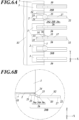
- FIG. 6A is a plan view showing the first lead terminals 20B, the second lead terminals 30 and their surroundings when the wiring substrate 10B of the second embodiment according to the present disclosure is viewed toward the first surface S1 of the substrate 1.
- FIG. 6B shows the first lead terminal(s) 20B and its surroundings when the wiring substrate 10B of the second embodiment according to the present disclosure is viewed from the side.
- the first lead terminals 20B are different from the first lead terminals 20A in that whereas in each first lead terminal 20A, the first tapered part 26a and the interconnecting part 26b lie on the substrate 1 in plan perspective view toward the first surface S1, in each first lead terminal 20B, only the first tapered part 26a lies on the substrate 1 in plan perspective view toward the first surface S1.
- Each of the first lead terminal 20A and the first lead terminal 20B has the first tapered part 26a located inside of the outer periphery of the substrate 1, and hence can increase, in mid-air, the region area of the part having a short distance D1 between the first lead terminal 20A/20B and the second lead terminal 30.
- the shape of the first lead terminal 20A in the wiring substrate 10A of the first embodiment 1 is advantageous in high-frequency properties because the shape can gain the region area of the part having a short distance D1 to the adjacent second lead terminal(s) 30, in particular in the case where dimensions of the lead part 27 are determined on the basis of an external board.
- FIG. 7A is a plan view showing the first lead terminals 20C, the second lead terminals 30 and their surroundings when the wiring substrate 10C of the third embodiment according to the present disclosure is viewed toward the first surface S1 of the substrate 1.
- FIG. 7B shows the first lead terminal(s) 20C and its surroundings when the wiring substrate 10C of the third embodiment according to the present disclosure is viewed from the side.
- the first lead terminals 20C are different from the first lead terminals 20A in that whereas in each first lead terminal 20A, the connecting part 26 has the first tapered part 26a, the interconnecting part 26b and the second tapered part 26c, in each first lead terminal 20C, the connecting part 26 is formed as a single rectangle when viewed in the XY plane, which is parallel to the first surface S1.
- the width at the contacting part 23 increases at once at the first bend 24, the increased width is kept unchanged from the first bend 24 to the second bend 25 and decreases at once at the second bend 25, and the decreased width is kept unchanged at the lead part 27.
- the first lead terminal 20C is more likely to reduce crosstalk due to increase in the volume and increase in the area of the part where the distance D1 to the second lead terminal 30 becomes the shortest.
- the wiring substrate 10C having such a first lead terminal (s) 20C is excellent in high-frequency properties. Since the first lead terminal 20C has the connecting part 26 that is rectangular when viewed in the XY plane, stress may concentrate on the corners. Hence, in the case where strength is required, the first lead terminal 20A is adopted over the first lead terminal 20C.
- FIG. 8A is a plan view showing the first lead terminals 20D, the second lead terminals 30 and their surroundings when the wiring substrate 10D of the fourth embodiment according to the present disclosure is viewed toward the first surface S1 of the substrate 1.
- FIG. 8B shows the first lead terminal(s) 20D and its surroundings when the wiring substrate 10D of the fourth embodiment according to the present disclosure is viewed from the side.
- the first lead terminals 20D are different from the first lead terminals 20A in that whereas in each first lead terminal 20A, the connecting part 26 has the first tapered part 26a, the interconnecting part 26b and the second tapered part 26c, in each first lead terminal 20D, the width at the contacting part 23 increases at once at the first bend 24, and the increased width is kept unchanged from the first bend 24 to the second end 22.
- the first lead terminal 20D is more likely to reduce crosstalk due to increase in the volume and increase in the area of the part where the distance D1 to the second lead terminal 30 becomes the shortest.
- the wiring substrate 10D having such a first lead terminal(s) 20D is excellent in high-frequency properties.
- FIG. 9A is a plan view showing the first lead terminals 20E, the second lead terminals 30 and their surroundings when the wiring substrate 10E of the fifth embodiment according to the present disclosure is viewed toward the first surface S1 of the substrate 1.
- FIG. 9B shows the first lead terminal(s) 20E and its surroundings when the wiring substrate 10E of the fifth embodiment according to the present disclosure is viewed from the side.
- the first lead terminals 20E are different from the first lead terminals 20A in that whereas in each first lead terminal 20A, the connecting part 26 has the first tapered part 26a, the interconnecting part 26b and the second tapered part 26c, in each first lead terminal 20E, the connecting part 26 has the first tapered part 26a and the second tapered part 26c, but does not have the interconnecting part 26b.
- the first lead terminal 20E configured without the interconnecting part 26b may be adopted.
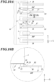
- FIG. 10A is a plan view showing the first lead terminals 20F, the second lead terminals 30 and their surroundings when the wiring substrate 10F of the sixth embodiment according to the present disclosure is viewed toward the first surface S1 of the substrate 1.
- FIG. 10B shows the first lead terminal (s) 20F and its surroundings when the wiring substrate 10F of the sixth embodiment according to the present disclosure is viewed from the side.
- the first lead terminals 20F are different from the first lead terminals 20A in the following two points. First, whereas in each first lead terminal 20A, the first tapered part 26a and the interconnecting part 26b lie on the substrate 1 in plan perspective view toward the first surface S1, in each first lead terminal 20F, only the first tapered part 26a lies on the substrate 1 in plan perspective view toward the first surface S1. Second, whereas in each first lead terminal 20A, both the second surface S2 and the third surface S3 are bent at the first bend 24 and the second bend 25, in each first lead terminal 20F, only the second surface S2 is bent at the first bend 24 and the second bend 25, and the third surface S3 is one flat surface from the first end 21 to the second end 22.
- the first lead terminal 20F has a changing thickness from the first end 21 to the second end 22. More specifically, in the first lead terminal 20F, the contacting part 23 is substantially uniformly thick, the lead part 27 is substantially uniformly thin, and the connecting part 26 becomes thinner from the connecting part 23 to the lead part 27.
- the first lead terminal 20F has an advantage over the first lead terminal 20A in increasing the volume of a lead terminal itself. Further, the lateral shape of the first lead terminal 20A reduces, when it is joined to an external board, flow of a joining material for connecting the upper surface of the external board to the third surface S3 of the first lead terminal 20F, such as a brazing material, to underneath the contacting part 23. This reduces change in impedance of the first lead terminal 20F and the second lead terminal 30. Hence, the wiring substrate 10A is stable in high-frequency properties.
- FIG. 11 is a plan view of a wiring substrate of a seventh embodiment according to the present disclosure when viewed toward a first surface of a substrate.
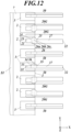
- FIG. 12 is an enlarged view of first lead terminals, second lead terminals and their surroundings shown in FIG. 11 .
- FIG. 13 shows the first lead terminal(s) and its surroundings when the wiring substrate of the seventh embodiment according to the present disclosure is viewed from the side.
- a wiring substrate 10G of the seventh embodiment is configured in the same manner as the wiring substrate 10A of the first embodiment except that arrangement of the first lead terminals and the second lead terminals in the wiring substrate 10A of the first embodiment is changed, and the first lead terminals 20A are replaced by first lead terminals 20G.
- the same components as those of the wiring substrate 10A of the first embodiment are denoted by the same reference signs as those used in the wiring substrate 10A to avoid duplicate descriptions, and different points from the wiring substrate 10A are mainly described.
- the ground conductors 2 and the signal conductors 3 are arranged along one short side of the first surface S1 such that two ground conductors 2 alternate with two signal conductors 3, and at each end, a ground conductor 2 is present.
- a ground conductor 2 and a signal conductor 3 adjacent to one another and signal conductors 3 adjacent to one another are arranged so as to be insulated from one another.
- a first lead terminal 20A is interposed between two second lead terminals 30.
- two second lead terminals 30 are interposed between first lead terminals 20G, which constitutes a GSSG (Ground/Signal/Signal/Ground) differential signal wiring.
- GSSG Ground/Signal/Signal/Ground
- a configuration in which a pair of first lead terminals 20G is interposed between second lead terminals 30 as a pair is repeated in the Y direction, so that the second lead terminals 30V and the first lead terminals 20A are adjacent to and aligned with one another in plan view.
- the connecting part 26 is composed of the first tapered part 26a, the interconnecting part 26b and the second tapered part 26c, and the sides along the length direction are substantially symmetrical about the center line that connects the center of the first end 21 and the center of the second end 22.
- the connecting part 26 is composed of the first tapered part 26a, the interconnecting part 26b and the second tapered part 26c, and the first tapered part 26a and the interconnecting part 26b are configured in the same manner as those of the first lead terminal 20A, but the second tapered part 26c of the connecting part 26 of the first lead terminal 20G is different from that of the first lead terminal 20A in that only the side opposite the adjacent second lead terminal 30, namely the side facing the adjacent first lead terminal 20G, is tapered.
- the sides along the length direction are not symmetrical about the center line that connects the center of the first end 21 and the center of the second end 22.
- the side close to the adjacent first lead terminal 20G namely the side facing the adjacent first lead terminal 20G, is configured in the same manner as that of the first lead terminal 20A.
- the side facing the adjacent first lead terminal 20G is inclined with respect to the direction from the first end 21 to the second end 22, so that the width W1 of the first lead terminal 20G thereat gradually decreases.
- the side of the first lead terminal 20G close to the adjacent second lead terminal 30, namely the side facing the adjacent second lead terminal 30, is configured differently from that of the first lead terminal 20A.
- the side facing the adjacent second lead terminal 30 gradually gets closer to the second lead terminal 30 at the first tapered part 26a and is parallel to the side(s) along the length direction of the second lead terminal 30 at the interconnecting part 26b, the second tapered part 26c and the lead part 27.
- the side facing the adjacent second lead terminal 30 is a straight line along the direction from the first end 21 to the second end 22, namely is parallel to the direction from the first end 21 to the second end 22.
- the first lead terminal 20G has an advantage over the first lead terminal 20A in further reducing crosstalk due to increase in the volume and increase in the area of the part where the distance D1 to the second lead terminal 30 becomes the shortest.
- FIG. 14 is a plan view showing first lead terminals, second lead terminals and their surroundings when a wiring substrate of an eighth embodiment according to the present disclosure is viewed toward a first surface of a substrate.
- the wiring substrate of the eighth embodiment is configured in the same manner as the wiring substrate 10A' as the modification of the first embodiment except that the first lead terminals 20A in the wiring substrate 10A' as the modification of the first embodiment are replaced by first lead terminals 20H.
- the same components as those of the wiring substrate 10A' as the modification of the first embodiment are denoted by the same reference signs as those used in the wiring substrate 10A' to avoid duplicate descriptions, and different points from the wiring substrate 10A' are mainly described.
- the wiring substrate of the eighth embodiment with the first lead terminals 20A replaced by the first lead terminals 20H is referred to as a wiring substrate 10H.
- Each first lead terminal 20H that the wiring substrate 10H has is configured by connecting, through a connecting part 28, the first ends 21 of first lead terminals 20A as a pair between which a pair of second lead terminals 30V in the wiring substrate 10A' is interposed.
- the first lead terminal 20H is configured by having two first lead terminals 20A detailed above as a set.
- the connecting part 28 is made of a metal material, and the metal material same as that of the first lead terminals 20A can be used, for example.
- the connecting part 28 is formed so as not to contact the signal conductors 3 with which the second lead terminals 30V as a pair located inside the first lead terminal 20H are in contact.
- the wiring substrate 10H having the above first lead terminals 20H can further reduce occurrence of crosstalk.
- the lower surfaces of the connecting parts 28 may be electrically connected to the ground conductors 2 by the ground conductors 2 being arranged so as to extend to underneath the connecting parts 28. This can further stabilize the ground of the wiring substrate 10A' and further reduce occurrence of crosstalk.
- FIG. 15 is an exploded perspective view of an electronic device of an embodiment according to the present disclosure.
- An electronic device 100 has the wiring substrate 10A of the first embodiment, an electronic component 11 mounted on the mounting part 5 of the wiring substrate 10A, and a lid 12.
- the electronic component 11 is, for example, a high-frequency semiconductor device.
- the semiconductor device include optical semiconductor devices, such as a light emitter and a light receiver.
- the semiconductor device may be another type of high-frequency semiconductor device, such as a sensor or an imager, as far as it can be housed in the wiring substrate.
- an optical fiber is connected and fixed to the through hole 6 provided in the frame 1b of the substrate 1.
- the electronic component 11 is, for example, a light emitter, such as an LD (laser diode)
- LD laser diode
- the electronic component 11 is, for example, a light receiver, such as a PD (photodiode), light output from the optical fiber is received by the light receiver, and an electric signal(s) corresponding to the amount of the received light is output to the outside via the first lead terminals 20A and the second lead terminals 30 that are respectively in contact with the ground conductors 2 and the signal conductors 3.
- a light receiver such as a PD (photodiode
- the lid 12 may be any type of lid as far as it prevents moisture, fine particles and so forth from entering the interior of the electronic device 100.
- the lid 12 usable may be formed, for example, by processing or molding the same metal material as that of the seal ring 4 or the same ceramic material as that of the substrate 1 into the shape of a plate.
- the electronic component 11 is an optical semiconductor device, such as an LD or a PD
- an opaque lid that hardly transmits light is used as the lid 12.
- the lid 12 is fixed to the upper surface of the seal ring 4 by seam welding or with a joining material. Examples of the joining material include a brazing material.
- the electronic device 100 of the embodiment uses the wiring substrate 10A of the first embodiment, thereby being an electronic device having improved impedance matching, reduced crosstalk, and excellent high-frequency properties.
- the wiring substrate has the coating member, but the coating member is not an essential component.
- the ground conductors 2 and the signal conductors 3 are spaced at regular intervals in the width direction, but arrangement of the ground conductors 2 and the signal conductors 3 is not limited thereto.
- a wiring substrate having improved high-frequency properties. Further, according to the present disclosure, there can be provided an electronic device having excellent high-frequency properties.
Landscapes
- Physics & Mathematics (AREA)
- Electromagnetism (AREA)
- Engineering & Computer Science (AREA)
- Microelectronics & Electronic Packaging (AREA)
- Condensed Matter Physics & Semiconductors (AREA)
- General Physics & Mathematics (AREA)
- Optics & Photonics (AREA)
- Structure Of Printed Boards (AREA)
- Printing Elements For Providing Electric Connections Between Printed Circuits (AREA)
- Lead Frames For Integrated Circuits (AREA)
Abstract
Description
- The present disclosure relates to a wiring substrate and an electronic device.
- In
Patent Literature 1, there is described a package for housing a high-frequency semiconductor device employing differential signaling as a transmission method. This package includes: a ceramic substrate; ground line conductors extending at right angles from the edge end of at least one side of the outer peripheral part of the lower surface of the ceramic substrate; and differential signal line conductors each composed of a pair of line conductors extending parallel to the ground line conductors and sandwiched between the ground line conductors on both sides. - Patent Literature 1:
JP 2016-146439 A - In a wiring substrate for mounting a high-frequency semiconductor device employing differential signaling as a transmission method, further improvement of high-frequency properties is desired.
- The present disclosure relates to a wiring substrate and an electronic device having improved high-frequency properties.
- A wiring substrate according to the present disclosure includes:
- a substrate having a first surface;
- a ground conductor on the first surface;
- a signal conductor on the first surface;
- a first lead terminal in contact with the ground conductor; and
- a second lead terminal in contact with the signal conductor and aligned with the first lead terminal,
- wherein the first lead terminal includes:
- a first end on the substrate in plan perspective view toward the first surface;
- a second end not on the substrate in the plan perspective view but at a position on an extension from the first end;
- a contacting part including the first end and in contact with the ground conductor;
- a connecting part including:
- a first bend away from the first end across the contacting part; and
- a second bend closer to the second end than the first bend; and
- a lead part connected to the second bend and extending to the second end, and
- wherein the connecting part includes a short-distance part having a shorter distance to the second lead terminal than the contacting part in plan view toward the first surface.
- An electronic device according to the present disclosure includes:
- the above wiring substrate; and
- an electronic component connected to the wiring substrate.
- According to the present disclosure, a wiring substrate having improved high-frequency properties can be provided. Further, according to the present disclosure, an electronic device having excellent high-frequency properties can be provided.
-
-
FIG. 1 is a perspective view showing a configuration of a wiring substrate of a first embodiment according to the present disclosure. -
FIG. 2 is a plan view of the wiring substrate shown inFIG. 1 when viewed toward a first surface of a substrate. -
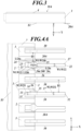
FIG. 3 is a side view of the wiring substrate shown inFIG. 1 . -
FIG. 4A is an enlarged view of first lead terminals, second lead terminals and their surroundings shown inFIG. 2 . -
FIG. 4B shows first lead terminals, second lead terminals and their surroundings in a modification of the wiring substrate of the first embodiment according to the present disclosure. -
FIG. 5 is an enlarged view of a first lead terminal and its surroundings shown inFIG. 3 . -
FIG. 6A is a plan view showing first lead terminals, second lead terminals and their surroundings when a wiring substrate of a second embodiment according to the present disclosure is viewed toward a first surface of a substrate. -
FIG. 6B shows the first lead terminal(s) and its surroundings when the wiring substrate of the second embodiment according to the present disclosure is viewed from the side. -
FIG. 7A is a plan view showing first lead terminals, second lead terminals and their surroundings when a wiring substrate of a third embodiment according to the present disclosure is viewed toward a first surface of a substrate. -
FIG. 7B shows the first lead terminal(s) and its surroundings when the wiring substrate of the third embodiment according to the present disclosure is viewed from the side. -
FIG. 8A is a plan view showing first lead terminals, second lead terminals and their surroundings when a wiring substrate of a fourth embodiment according to the present disclosure is viewed toward a first surface of a substrate. -
FIG. 8B shows the first lead terminal(s) and its surroundings when the wiring substrate of the fourth embodiment according to the present disclosure is viewed from the side. -
FIG. 9A is a plan view showing first lead terminals, second lead terminals and their surroundings when a wiring substrate of a fifth embodiment according to the present disclosure is viewed toward a first surface of a substrate. -
FIG. 9B shows the first lead terminal(s) and its surroundings when the wiring substrate of the fifth embodiment according to the present disclosure is viewed from the side. -
FIG. 10A is a plan view showing first lead terminals, second lead terminals and their surroundings when a wiring substrate of a sixth embodiment according to the present disclosure is viewed toward a first surface of a substrate. -
FIG. 10B shows the first lead terminal (s) and its surroundings when the wiring substrate of the sixth embodiment according to the present disclosure is viewed from the side. -
FIG. 11 is a plan view of a wiring substrate of a seventh embodiment according to the present disclosure when viewed toward a first surface of a substrate. -
FIG. 12 is an enlarged view of first lead terminals, second lead terminals and their surroundings shown inFIG. 11 . -
FIG. 13 shows the first lead terminal(s) and its surroundings when the wiring substrate of the seventh embodiment according to the present disclosure is viewed from the side. -
FIG. 14 is a plan view showing first lead terminals, second lead terminals and their surroundings when a wiring substrate of an eighth embodiment according to the present disclosure is viewed toward a first surface of a substrate. -
FIG. 15 is an exploded perspective view of an electronic device of an embodiment according to the present disclosure. - Hereinafter, embodiments of the present disclosure will be described with reference to the drawings. However, dimensions of components shown in the drawings do not faithfully represent the actual dimensions, dimensional ratios or the like of the components.
- As shown in
FIG. 1 to FIG. 5 , awiring substrate 10A of a first embodiment is a wiring substrate where an electronic component is to be mounted. The electronic component may be an electronic component that is driven at high frequency or an electronic component to and from which high-frequency signals are input and output. Thewiring substrate 10A includes asubstrate 1 having a first surface S1,ground conductors 2 located on the first surface S1, andsignal conductors 3 located on the first surface S1. - Hereinafter, directions of components of the
wiring substrate 10A will be described with an XYZ orthogonal coordinate system in which the thickness direction of thewiring substrate 10A is Z direction. The first surface S1 of thesubstrate 1 of thewiring substrate 10A is parallel to XY plane. Hereinafter, surfaces of each layer of thewiring substrate 10A facing +Z direction and -Z direction may be referred to as "upper surface" and "lower surface", respectively. - The
substrate 1 has a rectangular plate-like bottom 1a, and the lower surface of the bottom 1a constitutes the first surface S1. Thesubstrate 1 also has a frame 1b located on the upper surface of the bottom 1a along the outer periphery of the bottom 1a. The upper surface of the bottom 1a and the inner surface of the frame 1b form a cavity. The upper surface of the bottom 1a is a mounting surface having a mountingpart 5 where an electronic component is to be mounted. Thesubstrate 1 further has a throughhole 6 in a part of the frame 1b. Thewiring substrate 10A has aseal ring 4 on the upper surface of the frame 1b of thesubstrate 1. - The
substrate 1 is composed of a plurality of insulating substrates stacked on top of one another in the thickness direction, for example. As the insulating substrates, for example, a ceramic material, such as an aluminum oxide sintered body, a mullite sintered body, a silicon carbide sintered body, an aluminum nitride sintered body or a silicon nitride sintered body, or a glass ceramic material can be used. Theseal ring 4 is used as a seal material for airtight sealing with a lid after an electronic component is mounted on the mountingpart 5. Theseal ring 4 is configured, for example, such that a frame-shaped conductor made of conducive paste containing a high-melting-point metal, such as tungsten or molybdenum, is brazed and joined (bonded) to a frame-shaped metal plate made of an Fe-Ni-based alloy or an Fe-Ni-Co-based alloy with a brazing material or the like. - In the
wiring substrate 10A, the first surface S1 of thesubstrate 1 is, for example, rectangular, and has two long sides parallel to X direction and two short sides parallel to Y direction. As shown inFIG. 2 , in the case of the rectangular first surface S1, theground conductors 2 and thesignal conductors 3 are arranged along one short side of the first surface S1 such that oneground conductor 2 alternates with twosignal conductors 3, and at each end, aground conductor 2 is present. Aground conductor 2 and asignal conductor 3 adjacent to one another andsignal conductors 3 adjacent to one another are arranged so as to be insulated from one another. - The
ground conductors 2 and thesignal conductors 3 on the first surface S1 is, for example, rectangular and may have a predetermined width and a predetermined length inward from the edge of the short side of the first surface S1. Theground conductors 2 may be U-shaped so as to surround thesignal conductors 3. The "U-shaped" is, in other words, a shape formed by ends of twoground conductors 2 connected by a metallic object. Areas of theground conductors 2 and thesignal conductors 3 on the first surface S1 and spaces between theadjacent ground conductor 2 andsignal conductor 3 and between theadjacent signal conductors 3 thereon are appropriately determined on the basis of design of an electronic device to which thewiring substrate 10A is applied. Theground conductors 2 and thesignal conductors 3 contain a metal material, such as gold, silver, copper, nickel, tungsten, molybdenum or manganese. Theground conductors 2 and thesignal conductors 3 may be formed on the first surface S1 by co-firing with thesubstrate 1 in the form of a metallized layer(s), a plating layer(s) or the like or by metal plating. Theground conductors 2 and thesignal conductors 3 may have a substantially uniform thickness throughout, which may be about 5 to 30 µm. - The
ground conductors 2 and thesignal conductors 3 may be surrounded by acoating member 7. By theground conductors 2 and thesignal conductors 3 being surrounded by thecoating member 7, when theground conductors 2 and thesignal conductors 3 are respectively connected to first lead terminals and second lead terminals with a joining (bonding) material, the joining material is stemmed at boundaries between (i) theground conductors 2 and thesignal conductors 3 and (ii) thecoating member 7. This can reduce spread of the joining material on the first surface S1, and this reduction of spread of the joining material reduces change in inductance due to spread of the joining material, so that thewiring substrate 10A is impedance-matched. The reduction of spread of the joining material also results in forming a moderate fillet of the joining material, so that joining strength (bonding) of theground conductors 2 and the first lead terminals and joining (bonding) strength of thesignal conductors 3 and the second lead terminals increase. - The shape of the
coating member 7 is not limited to the above. For example, only either theground conductors 2 or thesignal conductors 3 may be surrounded by thecoating member 7. Alternatively, thecoating member 7 may be arranged so as to surround eachground conductor 2 and also surround twoadjacent signal conductors 3 collectively. In any case, reduction of spread of the joining material results in forming a moderate fillet of the joining material, so that joining strength of theground conductors 2 and the first lead terminals and joining strength of thesignal conductors 3 and the second lead terminals increase. The shape of the coating member so as to surround twoadjacent signal conductors 3 collectively can also achieve miniaturization of thewiring substrate 10A in addition to increase in the joining strength. - As the
coating member 7, for example, a ceramic material, such as an aluminum oxide sintered body, a chromium sintered body, a mullite sintered body, a silicon carbide sintered body, an aluminum nitride sintered body or a silicon nitride sintered body, or a glass ceramic material can be used. - The
wiring substrate 10A hasfirst lead terminals 20A that are in contact with therespective ground conductors 2 andsecond lead terminals 30 that are aligned with thefirst lead terminals 20A and in contact with therespective signal conductors 3. Thefirst lead terminals 20A and thesecond lead terminals 30 extend at right angles to, of the first surface S1, the short side(s) that is parallel to the Y direction, namely extend parallel to the X direction. Thefirst lead terminals 20A and thesecond lead terminals 30 are, for example, connected to outside, so that an electronic component mounted on the mountingpart 5 of thesubstrate 1 outputs and receives electric signals to and from the outside. - The bottom 1a of the
substrate 1 is, for example, mainly composed of an insulating substrate(s), and has a wiring conductor(s), a through conductor(s) and/or the like therein so that an electronic component or its peripheral components on the mountingpart 5 of the upper surface are electrically connected to theground conductors 2 and thesignal conductors 3 on the lower surface. This allows an electronic component mounted on the mountingpart 5 to output and receive electric signals to and from the outside via thefirst lead terminals 20A and thesecond lead terminals 30 that are respectively in contact with theground conductors 2 and thesignal conductors 3. - The
first lead terminals 20A and thesecond lead terminals 30 are made of a metal material, and for example, after molded into the shapes described below, respectively joined to theground conductors 2 and thesignal conductors 3 with a joining material, such as a brazing material. The material of thefirst lead terminals 20A and thesecond lead terminals 30 may be a metal, such as copper, iron, nickel, cobalt or chromium, or a metallic alloy containing such a metal, for example. - Each first
lead terminal 20A has afirst end 21 at a position on thesubstrate 1 in plan perspective view toward the first surface S1 and asecond end 22 not on thesubstrate 1 but at a position on an extension from thefirst end 21 in parallel to the X direction. Thefirst lead terminal 20A has a contactingpart 23, a connectingpart 26 and alead part 27 in this order from thefirst end 21 to thesecond end 22. Thefirst lead terminal 20A has a second surface S2 facing the first surface S1 and a third surface S3 opposite the second surface S2. Thefirst lead terminal 20A may be a long, narrow plate having predetermined width, length and thickness, for example. In this embodiment, thefirst lead terminal 20A has a substantially uniform thickness along the length direction. The width direction, length direction and thickness direction of thefirst lead terminal 20A are a direction parallel to the Y direction, a direction parallel to the X direction and a direction parallel to the Z direction, respectively. - The contacting
part 23 is a part that includes thefirst end 21 and at which the second surface S2 contacts theground conductor 2. The connectingpart 26 is a part that includes afirst bend 24 at a positon away from thefirst end 21 across the contactingpart 23 and asecond bend 25 at a position closer to thesecond end 22 than thefirst bend 24. Thefirst bend 24 is where the second surface S2 separates from theground conductor 2. More specifically, the contactingpart 23 is a part from thefirst end 21 to thefirst bend 24, and the connectingpart 26 is a part from thefirst bend 24 to thesecond bend 25. Thelead part 27 is a part connected to thesecond bend 25 and extending to thesecond end 22. - The
first bend 24 is where thefirst lead terminal 20A is bent in the -Z direction, namely downward, so as to separate from theground conductor 2. Thesecond bend 25 is where thefirst lead terminal 20A is bent in the +Z direction, namely upward, with respect to the bending direction at thefirst bend 24. In the case of thefirst lead terminal 20A, the entirefirst lead terminal 20A is bent at thefirst bend 24 and thesecond bend 25, but like a first lead terminal (s) 20F described below, only the second surface S2 may be bent at thefirst bend 24 and thesecond bend 25. That is, in a wiring substrate of an embodiment, at least the second surface of each first lead terminal has a first bend and a second bend. - The
first lead terminal 20A having thefirst bend 24, thesecond bend 25 or both can absorb, with thefirst bend 24 or thesecond bend 25, pressure applied to thefirst lead terminal 20A when an external board is connected to thewiring substrate 10A. This can reduce occurrence of damage to thefirst lead terminal 20A. - The second surface S2 of the
first lead terminal 20A is, for example, a surface parallel to the first surface S1 at the contactingpart 23, a surface having a predetermined angle to the first surface S1 at the connectingpart 26, and a surface parallel to the first surface S1 at thelead part 27. InFIG. 5 , an angle formed by the second surface S2 at the connectingpart 26 and a plane obtained by extending the second surface S2 at the contactingpart 23 is represented by "α1". The angle α1 may range from 20 to 60 degrees, for example. Further, inFIG. 5 , an angle formed by the second surface S2 at the connectingpart 26 and the second surface S2 at thelead part 27 is represented by "β1". In the case where the second surface S2 of thefirst lead terminal 20A is a surface parallel to the first surface S1 at thelead part 27, the angle β1 is expressed by "180 - α1". - As shown in
FIG. 5 , the entirefirst lead terminal 20A is bent at thefirst bend 24 and thesecond bend 25. The third surface S3 may have the same shape as the second surface S2, for example. For example, in the case where an angle formed by the third surface S3 at the contactingpart 23 and the third surface S3 at the connectingpart 26 is represented by "β2", and an angle formed by the third surface S3 at the connectingpart 26 and a plane obtained by extending the third surface S3 at thelead part 27 is represented by "α2", "Angle β2 ≈ Angle β1" and "Angle α2 ≈ Angle α1" may hold. Thelead part 27 is, for example, a part that is connected to an external board, such as a flexible board, such that the third surface S3 at thelead part 27 contacts the upper surface of the external board. - In the
first lead terminal 20A, the connectingpart 26 is a part that is not in contact with either theground conductor 2 or an external board and is located in a region in mid-air. Distance H between the plane obtained by extending the second surface S2 of thefirst lead terminal 20A at the contactingpart 23 and the second surface S2 thereof at thelead part 27 may be about 0.1 to 0.5 mm. - When the
first lead terminal 20A is viewed in the XY plane, which is parallel to the first surface S1, the connectingpart 26 has a part having a shorter distance D1 to the second lead terminal(s) 30 than the contacting part 23 (FIG. 4A ). More specifically, the connectingpart 26 is composed of a firsttapered part 26a, a secondtapered part 26c and an interconnectingpart 26b. The firsttapered part 26a is a part where a width W1 increases toward thesecond end 22. The secondtapered part 26b is a part that is located closer to thesecond end 22 than the firsttapered part 26a and where the width W1 decreases toward (to) thelead part 27. The interconnectingpart 26c is a part that is located between the firsttapered part 26a and the secondtapered part 26c. The firsttapered part 26a is a region from thefirst bend 24 to its boundary with the interconnectingpart 26b, and the secondtapered part 26c is a region from its boundary with the interconnectingpart 26b to thesecond bend 25. - In the
wiring substrate 10A, except for thefirst lead terminals 20A located at both ends of the first surface S1 of thesubstrate 1 in the Y direction, eachfirst lead terminal 20A is interposed between twosecond lead terminals 30. Thefirst lead terminal 20A has the width W1 that gradually increases at the firsttapered part 26a such that the sides extending in the length direction (X direction) are spread in the width direction (Y direction) until they reach the interconnectingpart 26b. Thefirst lead terminal 20A has the width W1 that is kept unchanged at the interconnectingpart 26b from thefirst end 21 toward thesecond end 22. That is, the width W1 at the interconnectingpart 26b is uniform. This makes it possible to stably adjust impedance. Thefirst lead terminal 20A has the width W1 that gradually decreases at the secondtapered part 26c such that the sides extending in the length direction (X direction) get closer in the width direction (Y direction). The sides of thefirst lead terminal 20A extending in the length direction are substantially symmetrical about a center line that connects the center of thefirst end 21 and the center of thesecond end 22. In the above, the width W1 at the firsttapered part 26a may gradually increase from thefirst end 21 toward thesecond end 22 at a predetermined rate, and/or the width W1 at the secondtapered part 26c may gradually decrease from thefirst end 21 toward thesecond end 22 at a predetermined rate. This can gradually change impedance at thesignal conductor 3 and thesecond lead terminal 30 that are adjacent to thefirst lead terminal 20A and hence makes impedance adjustment easy. - As described below, the dimension in the length direction of the
second lead terminals 30 may be the same as that of thefirst lead terminals 20A. That is, thesecond lead terminals 30 and thefirst lead terminals 20A may have the same length. Thesecond lead terminals 30 are parallel to thefirst lead terminals 20A. Eachsecond lead terminal 30 has a predetermined narrow width W2 that is set, for example, in conformity with desired high-frequency properties and strength. In order to transmit high-frequency signals, thesecond lead terminal 30 is formed such that the width W2 does not greatly change. Afirst lead terminal 20A and twosecond lead terminals 30 between which thefirst lead terminal 20A is interposed having their respective configurations described above allow thefirst lead terminal 20A to have, at the interconnectingpart 26b of the connectingpart 26, the shortest distance D1 to each of thesecond lead terminals 30 located on both sides. In this embodiment, the distance D1 between afirst lead terminal 20A and asecond lead terminal 30 located on one side of thefirst lead terminal 20A is the same as the distance D1 between thefirst lead terminal 20A and asecond lead terminal 30 located on the other side thereof. - At the part at which the distance D1 between the
first lead terminal 20A and each of thesecond lead terminals 30 becomes the shortest, the distance D1 may be about 0.2 to 1.0 mm, for example. Thefirst lead terminal 20A having, in the connectingpart 26 located in mid-air, a part having a short distance D1 to each of thesecond lead terminals 30 makes impedance matching easy. Hence, thewiring substrate 10A is excellent in high-frequency properties. Further, thefirst lead terminal 20A having a wide width W1 at the connectingpart 26 can have a large volume. This reduces occurrence of crosstalk. Hence, thewiring substrate 10A is excellent in high-frequency properties. - The
first lead terminal 20A including the connectingpart 26 having the firsttapered part 26a, the interconnectingpart 26b and the secondtapered part 26c has the following advantages. Thefirst lead terminal 20A having the firsttapered part 26a and the secondtapered part 26c is easy to process. That is, thefirst lead terminal 20A has higher workability than that having a corner(s) of an exterior angle of less than 90 degrees at a point(s) at/from which the width W1 changes. Further, thefirst lead terminal 20A having the firsttapered part 26a and the secondtapered part 26c has less stress concentration at a point(s) at/from which the width W1 changes than that having a corner(s) of an exterior angle of, for example, 90 degrees at a point(s) at/from which the width W1 changes. This can reduce, in thefirst lead terminal 20A, appearance of cracks or the like due to pressure or the like from the outside. - The width W1 of the
first lead terminal 20A at thelead part 27 is determined by design of an external board, for example. If the set width W1 at thelead part 27 is narrow, it is, for the reasons described above, advantageous to thefirst lead terminal 20A to have the secondtapered part 26c. In thefirst lead terminal 20A, the interconnectingpart 26b is the part where the width W1 becomes the largest. In order to increase the volume of thefirst lead terminal 20A and increase the area of the part where the distance D1 between thefirst lead terminal 20A and thesecond lead terminal 30 becomes the shortest, it is advantageous to the interconnectingpart 26b to have a longer length. However, if the length of the interconnectingpart 26b is increased, the sides along the length direction are bent at approximately 90 degrees at points of the firsttapered part 26a, the points where the width W1 starts and finishes increasing, and at points of the secondtapered part 26c, the points where the width W1 starts and finishes decreasing. As a result, stress concentrates on the firsttapered part 26a and the secondtapered part 26c. This could be disadvantageous in terms of strength. - Hence, the ratio of the lengths of the first
tapered part 26a, the interconnectingpart 26b and the secondtapered part 26c of thefirst lead terminal 20A can be appropriately selected with a balance between workability and volume increase taken into account. In thefirst lead terminal 20A, the firsttapered part 26a and the interconnectingpart 26b lie on thesubstrate 1 in plan perspective view toward the first surface S1. The firsttapered part 26a that is located inside of the outer periphery of thesubstrate 1 and bent can increase, in mid-air, the area of the part having a short distance D1 between thefirst lead terminal 20A and thesecond lead terminal 30. In mid-air, what surrounds thefirst lead terminal 20A is air having a lower dielectric constant than thesubstrate 1. Hence, the distance D1 between thefirst lead terminal 20A and thesecond lead terminal 30 being short makes impedance adjustment of thefirst lead terminal 20A and thesecond lead terminal 30 easy. - Each
second lead terminal 30 has afirst end 31 and asecond end 32. Thefirst end 31 is at a position on thesubstrate 1 in plan perspective view toward the first surface S1. Thesecond end 32 is not on thesubstrate 1 but at a position on an extension from thefirst end 31 in parallel to the X direction. Thesecond lead terminal 30 has a contactingpart 33, a connectingpart 36 and alead part 37 in this order from thefirst end 31 to thesecond end 32. Thesecond lead terminal 30 has a fourth surface facing the first surface S1 and a fifth surface opposite the fourth surface. Thesecond lead terminal 30 may be a long, narrow plate having predetermined width, length and thickness, for example. In this embodiment, thesecond lead terminal 30 has a substantially uniform thickness along the length direction, like thefirst lead terminal 20A. - The width direction, length direction and thickness direction of the
second lead terminal 30 may coincide with the width direction, length direction and thickness direction of thefirst lead terminal 20A, respectively. More specifically, the width direction, length direction and thickness direction of thesecond lead terminal 30 are a direction parallel to the Y direction, a direction parallel to the X direction and a direction parallel to the Z direction, respectively. - As shown in
FIG. 4A , the width of thesecond lead terminal 30 on thesecond end 32 side may be the same as the width of thefirst lead terminal 20A on thesecond end 22 side. Since thefirst lead terminal 20A has the above-described configuration, the width W1 (W122) of thefirst lead terminal 20A on thesecond end 22 side is smaller than the width W1 (W121) of thefirst lead terminal 20A on thefirst end 21 side. Meanwhile, the width W2 (W232) of thesecond lead terminal 30 on thesecond end 32 side is the same as the width W2 (W231) of thesecond lead terminal 30 on thefirst end 31 side. Hence, in this embodiment, "Width W121 > Width W122 = Width W231 = Width W232" holds. - In the case where the width at the interconnecting
part 26b is represented by W126b, "Width 126b > Width W121 > Width W122" may hold. That is, "Difference between Width W126b and Width W121 > Difference between Width W126b and Width W122" may hold. In this case, stable impedance adjustment and package miniaturization can be achieved appropriately. - Further, as shown in
FIG. 4A , the length (dimension in the length direction) L1 of thefirst lead terminal 20A may have the following relationship at the connectingpart 26. In the case where the length at the firsttapered part 26a is represented by L126a, and the length at the secondtapered part 26c is represented by L126c, "L126a < L126c" may hold. In this case, stable impedance adjustment and package miniaturization can be achieved appropriately. Further, in the case where the length at the interconnectingpart 26b is represented by L126b, "L126a < L126c < L126b" may hold. - The contacting
part 33 of thesecond lead terminal 30 is a part that includes thefirst end 31 and at which the fourth surface contacts thesignal conductor 3. The connectingpart 36 of thesecond lead terminal 30 is a part that includes afirst bend 34 at a position away from thefirst end 31 across the contactingpart 33 and asecond bend 35 at a position closer to thesecond end 32 than thefirst bend 34. Thefirst bend 34 is where the fourth surface separates from thesignal conductor 3. More specifically, the contactingpart 33 of thesecond lead terminal 30 is a part from thefirst end 31 to thefirst bend 34, and the connectingpart 36 of thesecond lead terminal 30 is a part from thefirst bend 34 to thesecond bend 35. Thelead part 37 of thesecond lead terminal 30 is a part connected to thesecond bend 35 and extending to thesecond end 32. - The
second lead terminal 30 may have the same lateral shape as thefirst lead terminal 20A, for example. In thesecond lead terminal 30, thefirst bend 34 is where thesecond lead terminal 30 is bent in the -Z direction, namely downward, so as to separate from thesignal conductor 3, and thesecond bend 35 is where thesecond lead terminal 30 is bent in the +Z direction, namely upward, with respect to the bending direction at thefirst bend 34. Thesecond lead terminal 30 having thefirst bend 34, thesecond bend 35 or both can reduce, with thefirst bend 34 or thesecond bend 35, pressure applied to thesecond lead terminal 30 when an external board is connected to thewiring substrate 10A. This can reduce occurrence of damage to thesecond lead terminal 30. - The fourth surface of the
second lead terminal 30 is, for example, a surface parallel to the first surface S1 at the contactingpart 33, a surface having a predetermined angle to the first surface S1 at the connectingpart 36, and a surface parallel to the first surface S1 at thelead part 37. An angle formed by the fourth surface at the connectingpart 36 and a plane obtained by extending the fourth surface at the contactingpart 33 may be in the same range as the angle α1. Further, an angle formed by the fourth surface at the connectingpart 36 and the fourth surface at thelead part 37 may be in the same range as the angle β1. - The entire
second lead terminal 30 is bent at thefirst bend 34 and thesecond bend 35. The fifth surface may have the same shape as the fourth surface. Thelead part 37 of thesecond lead terminal 30 is, for example, a part that is connected to an external board, such as a flexible board, such that the fifth surface at thelead part 37 contacts the upper surface of the external board. The fifth surface of thesecond lead terminal 30 at thelead part 37 is usually on the same plane as the third surface S3 of thefirst lead terminal 20A at thelead part 27. In thesecond lead terminal 30, the connectingpart 36 is a part that is not in contact with either thesignal conductor 3 or an external board and is located in a region in mid-air. - When the
second lead terminal 30 is viewed in the XY plane, which is parallel to the first surface S1, the width W2 of thesecond lead terminal 30 may be uniform at the contactingpart 33, the connectingpart 36 and the lead part 37 (FIG. 4A ). Hence, distance D2 between twosecond lead terminals 30 adjacent to one another is kept uniform from the first end(s) 31 to the second end(s) 32 of the second lead terminal(s) 30. In contrast, the distance D1 between asecond lead terminal 30 and afirst lead terminal 20A adjacent to one another becomes the shortest at the interconnectingpart 26b of the connectingpart 26 of thefirst lead terminal 20A. -
FIG. 4B is an enlarged view of first lead terminals, second lead terminals and their surroundings in awiring substrate 10A' as a modification of thewiring substrate 10A of the first embodiment. Thewiring substrate 10A' is configured in the same manner as thewiring substrate 10A of the first embodiment except that thesecond lead terminals 30 in thewiring substrate 10A of the first embodiment are replaced bysecond lead terminals 30V. Hereinafter, regarding thewiring substrate 10A', thesecond lead terminals 30V, which are different from thesecond lead terminals 30, are mainly described. - In the
wiring substrate 10A', thesecond lead terminals 30V and thefirst lead terminals 20A are arranged so as to be adjacent to one another in plan view as in thewiring substrate 10A. More specifically, a configuration in which onefirst lead terminal 20A is interposed betweensecond lead terminals 30V as a pair is repeated in the Y direction, so that thesecond lead terminals 30V and thefirst lead terminals 20A are adjacent to and aligned with one another in plan view. This arrangement constitutes GSSG (Ground/Signal/Signal/Ground) differential signal wirings. As in the embodiment, G (Ground) in GSSG may be shared by differential signal wirings adjacent to one another. - Each
second lead terminal 30V has thefirst end 31 and thesecond end 32, like eachsecond lead terminal 30. Thesecond lead terminal 30V has the contactingpart 33, the connectingpart 36 and thelead part 37 in this order from thefirst end 31 to thesecond end 32. Thesecond lead terminal 30V has the fourth surface facing the first surface S1 and the fifth surface opposite the fourth surface. - The
second lead terminal 30V has a thirdtapered part 36b at which, in plan view, the side of thesecond lead terminal 30V facing thefirst lead terminal 20A adjacent to thesecond lead terminal 30V has a shorter distance to thefirst lead terminal 20A as the side further separates from thesignal conductor 3. The side facing thefirst lead terminal 20A adjacent to thesecond lead terminal 30V is, of the two sides of thesecond lead terminal 30V extending in the length direction, the side close to the adjacentfirst lead terminal 20A. Thesecond lead terminal 30V provided with this thirdtapered part 36 can secure the width of thesecond lead terminal 30V on thesecond end 32 side so as to conform to standards and gradually change impedance of thesecond lead terminal 30V, and also can make the width of thesecond lead terminal 30V on thefirst end 31 side small and make the width of thesignal conductor 3 small accordingly. As a result, both easy impedance adjustment and wiring substrate miniaturization can be achieved. - The third
tapered part 36b can be provided, for example, in the connectingpart 36 of thesecond lead terminal 30V. In this case, the contactingpart 33, the connectingpart 36 and thelead part 37 of thesecond lead terminal 30V are the same as those of thesecond lead terminal 30 except that the connectingpart 36 has the thirdtapered part 36b at which the width W2 gradually increases. The connectingpart 36 has, for example, a first interconnectingpart 36a, the thirdtapered part 36b and asecond interconnecting part 36c in this order from thefirst end 31 side toward thesecond end 32. At the first interconnectingpart 36a, the width W2 of thesecond lead terminal 30V is uniform. At the thirdtapered part 36b, the width W2 of thesecond lead terminal 30V increases from thefirst end 31 side toward thesecond end 32. At the second interconnectingpart 36c, the increased width W2 is kept as it is. - In the
wiring substrate 10A', the width W1 of thefirst lead terminal 20A at the interconnectingpart 26b, namely the width W1 at the part having a short distance (short-distance part) to thesecond lead terminal 30V, is uniform, and, in plan view, the thirdtapered part 36b of thesecond lead terminal 30V is adjacent to the interconnectingpart 26b of thefirst lead terminal 20A. In thesecond lead terminal 30V shown inFIG. 4B , the thirdtapered part 36b is, over its entire length in the length direction, adjacent to the interconnectingpart 26b of thefirst lead terminal 20A. However, arrangement of the thirdtapered part 36b is not limited thereto. The thirdtapered part 36b is at least partly adjacent to the interconnectingpart 26b of thefirst lead terminal 20A. Thesecond lead terminal 30V having this thirdtapered part 36b makes it easy to stably adjust impedance. - Regarding the
second lead terminal 30V shown inFIG. 4B , the position of the thirdtapered part 36b is described in detail. In plan view, in a direction from thefirst end 21 to thesecond end 22 of thefirst lead terminal 20A, namely the X direction, an end of the interconnectingpart 26b (short-distance part to thesecond lead terminal 30V) of thefirst lead terminal 20A close to theground conductor 2 is represented by E1, and an end of the interconnectingpart 26b (short-distance part to thesecond lead terminal 30V) of thefirst lead terminal 20A far from theground conductor 2 is represented by E2. Further, in plan view, in the X direction, an end of the thirdtapered part 36b close to thesignal conductor 3 is represented by E3, and an end of the thirdtapered part 36b far from thesignal conductor 3 is represented by E4. In this case, the end E3 of the thirdtapered part 36b is, in plan view, closer to thesecond end 22 than the end E1 of the interconnectingpart 26b of thefirst lead terminal 20A. Further, the end E4 of the thirdtapered part 36b is, in plan view, closer to thefirst end 21 than the end E2 of the interconnectingpart 26b of thefirst lead terminal 20A. This arrangement of the thirdtapered part 36b of thesecond lead terminal 30V can achieve both easy impedance adjustment and wiring substrate miniaturization. - In this embodiment too, as shown in
FIG. 4B , the width of thesecond lead terminal 30V on thesecond end 32 side may be the same as the width of thefirst lead terminal 20A on thesecond end 22 side. As in the case shown inFIG. 4A , the width W1 (W122) of thefirst lead terminal 20A on thesecond end 22 side is smaller than the width W1 (W121) of thefirst lead terminal 20A on thefirst end 21 side. Meanwhile, unlike the case shown inFIG. 4A , the width W2 (W232) of thesecond lead terminal 30V on thesecond end 32 side is larger than the width W2 (W231) of thesecond lead terminal 30V on thefirst end 31 side. Hence, in this embodiment, "Width W121 > Width W122 = Width W232 > Width W231" holds. - Wiring substrates of second to sixth embodiments are configured in the same manner as the
wiring substrate 10A of the first embodiment except that thefirst lead terminals 20A in thewiring substrate 10A of the first embodiment are replaced byfirst lead terminals 20B to 20F. In the following descriptions of the wiring substrates of the second to sixth embodiments, the same components as those of thewiring substrate 10A of the first embodiment are denoted by the same reference signs as those used in thewiring substrate 10A to avoid duplicate descriptions, and different points from thewiring substrate 10A are mainly described. - Hereinafter, the wiring substrate of the second embodiment with the
first lead terminals 20A replaced by thefirst lead terminals 20B is referred to as a wiring substrate 10B, the wiring substrate of the third embodiment with thefirst lead terminals 20A replaced by thefirst lead terminals 20C is referred to as a wiring substrate 10C, the wiring substrate of the fourth embodiment with thefirst lead terminals 20A replaced by thefirst lead terminals 20D is referred to as a wiring substrate 10D, the wiring substrate of the fifth embodiment with thefirst lead terminals 20A replaced by thefirst lead terminals 20E is referred to as a wiring substrate 10E, and the wiring substrate of the sixth embodiment with thefirst lead terminals 20A replaced by thefirst lead terminals 20F is referred to as a wiring substrate 10F. -
FIG. 6A is a plan view showing thefirst lead terminals 20B, thesecond lead terminals 30 and their surroundings when the wiring substrate 10B of the second embodiment according to the present disclosure is viewed toward the first surface S1 of thesubstrate 1.FIG. 6B shows the first lead terminal(s) 20B and its surroundings when the wiring substrate 10B of the second embodiment according to the present disclosure is viewed from the side. - The
first lead terminals 20B are different from thefirst lead terminals 20A in that whereas in eachfirst lead terminal 20A, the firsttapered part 26a and the interconnectingpart 26b lie on thesubstrate 1 in plan perspective view toward the first surface S1, in eachfirst lead terminal 20B, only the firsttapered part 26a lies on thesubstrate 1 in plan perspective view toward the first surface S1. - Each of the
first lead terminal 20A and thefirst lead terminal 20B has the firsttapered part 26a located inside of the outer periphery of thesubstrate 1, and hence can increase, in mid-air, the region area of the part having a short distance D1 between thefirst lead terminal 20A/20B and thesecond lead terminal 30. This makes impedance adjustment easy, and hence thewiring substrate 10A/10B of the first/second embodiment can be easily impedance-matched to a desired value. It is noted that the shape of thefirst lead terminal 20A in thewiring substrate 10A of thefirst embodiment 1 is advantageous in high-frequency properties because the shape can gain the region area of the part having a short distance D1 to the adjacent second lead terminal(s) 30, in particular in the case where dimensions of thelead part 27 are determined on the basis of an external board. -
FIG. 7A is a plan view showing thefirst lead terminals 20C, thesecond lead terminals 30 and their surroundings when the wiring substrate 10C of the third embodiment according to the present disclosure is viewed toward the first surface S1 of thesubstrate 1.FIG. 7B shows the first lead terminal(s) 20C and its surroundings when the wiring substrate 10C of the third embodiment according to the present disclosure is viewed from the side. - The
first lead terminals 20C are different from thefirst lead terminals 20A in that whereas in eachfirst lead terminal 20A, the connectingpart 26 has the firsttapered part 26a, the interconnectingpart 26b and the secondtapered part 26c, in eachfirst lead terminal 20C, the connectingpart 26 is formed as a single rectangle when viewed in the XY plane, which is parallel to the first surface S1. In thefirst lead terminal 20C, the width at the contactingpart 23 increases at once at thefirst bend 24, the increased width is kept unchanged from thefirst bend 24 to thesecond bend 25 and decreases at once at thesecond bend 25, and the decreased width is kept unchanged at thelead part 27. - In the
first lead terminal 20C, an area (region) where the distance D1 between thefirst lead terminal 20C and thesecond lead terminal 30 becomes the shortest, namely an area (region) where the width W1 of thefirst lead terminal 20C becomes the largest, is the entire connectingpart 26. As compared with thefirst lead terminal 20A, thefirst lead terminal 20C is more likely to reduce crosstalk due to increase in the volume and increase in the area of the part where the distance D1 to thesecond lead terminal 30 becomes the shortest. The wiring substrate 10C having such a first lead terminal (s) 20C is excellent in high-frequency properties. Since thefirst lead terminal 20C has the connectingpart 26 that is rectangular when viewed in the XY plane, stress may concentrate on the corners. Hence, in the case where strength is required, thefirst lead terminal 20A is adopted over thefirst lead terminal 20C. -
FIG. 8A is a plan view showing thefirst lead terminals 20D, thesecond lead terminals 30 and their surroundings when the wiring substrate 10D of the fourth embodiment according to the present disclosure is viewed toward the first surface S1 of thesubstrate 1.FIG. 8B shows the first lead terminal(s) 20D and its surroundings when the wiring substrate 10D of the fourth embodiment according to the present disclosure is viewed from the side. - The
first lead terminals 20D are different from thefirst lead terminals 20A in that whereas in eachfirst lead terminal 20A, the connectingpart 26 has the firsttapered part 26a, the interconnectingpart 26b and the secondtapered part 26c, in eachfirst lead terminal 20D, the width at the contactingpart 23 increases at once at thefirst bend 24, and the increased width is kept unchanged from thefirst bend 24 to thesecond end 22. - As compared with the
first lead terminal 20A and even compared with thefirst lead terminal 20C, thefirst lead terminal 20D is more likely to reduce crosstalk due to increase in the volume and increase in the area of the part where the distance D1 to thesecond lead terminal 30 becomes the shortest. The wiring substrate 10D having such a first lead terminal(s) 20D is excellent in high-frequency properties. -
FIG. 9A is a plan view showing thefirst lead terminals 20E, thesecond lead terminals 30 and their surroundings when the wiring substrate 10E of the fifth embodiment according to the present disclosure is viewed toward the first surface S1 of thesubstrate 1.FIG. 9B shows the first lead terminal(s) 20E and its surroundings when the wiring substrate 10E of the fifth embodiment according to the present disclosure is viewed from the side. - The
first lead terminals 20E are different from thefirst lead terminals 20A in that whereas in eachfirst lead terminal 20A, the connectingpart 26 has the firsttapered part 26a, the interconnectingpart 26b and the secondtapered part 26c, in eachfirst lead terminal 20E, the connectingpart 26 has the firsttapered part 26a and the secondtapered part 26c, but does not have the interconnectingpart 26b. In terms of impedance adjustment according to the connecting condition with thesignal conductor 3 or an external board, thefirst lead terminal 20E configured without the interconnectingpart 26b may be adopted. -
FIG. 10A is a plan view showing thefirst lead terminals 20F, thesecond lead terminals 30 and their surroundings when the wiring substrate 10F of the sixth embodiment according to the present disclosure is viewed toward the first surface S1 of thesubstrate 1.FIG. 10B shows the first lead terminal (s) 20F and its surroundings when the wiring substrate 10F of the sixth embodiment according to the present disclosure is viewed from the side. - The
first lead terminals 20F are different from thefirst lead terminals 20A in the following two points. First, whereas in eachfirst lead terminal 20A, the firsttapered part 26a and the interconnectingpart 26b lie on thesubstrate 1 in plan perspective view toward the first surface S1, in eachfirst lead terminal 20F, only the firsttapered part 26a lies on thesubstrate 1 in plan perspective view toward the first surface S1. Second, whereas in eachfirst lead terminal 20A, both the second surface S2 and the third surface S3 are bent at thefirst bend 24 and thesecond bend 25, in eachfirst lead terminal 20F, only the second surface S2 is bent at thefirst bend 24 and thesecond bend 25, and the third surface S3 is one flat surface from thefirst end 21 to thesecond end 22. That is, whereas thefirst lead terminal 20A has a substantially uniform thickness from thefirst end 21 to thesecond end 22, thefirst lead terminal 20F has a changing thickness from thefirst end 21 to thesecond end 22. More specifically, in thefirst lead terminal 20F, the contactingpart 23 is substantially uniformly thick, thelead part 27 is substantially uniformly thin, and the connectingpart 26 becomes thinner from the connectingpart 23 to thelead part 27. - The
first lead terminal 20F has an advantage over thefirst lead terminal 20A in increasing the volume of a lead terminal itself. Further, the lateral shape of thefirst lead terminal 20A reduces, when it is joined to an external board, flow of a joining material for connecting the upper surface of the external board to the third surface S3 of thefirst lead terminal 20F, such as a brazing material, to underneath the contactingpart 23. This reduces change in impedance of thefirst lead terminal 20F and thesecond lead terminal 30. Hence, thewiring substrate 10A is stable in high-frequency properties. -
FIG. 11 is a plan view of a wiring substrate of a seventh embodiment according to the present disclosure when viewed toward a first surface of a substrate.FIG. 12 is an enlarged view of first lead terminals, second lead terminals and their surroundings shown inFIG. 11 .FIG. 13 shows the first lead terminal(s) and its surroundings when the wiring substrate of the seventh embodiment according to the present disclosure is viewed from the side. - A
wiring substrate 10G of the seventh embodiment is configured in the same manner as thewiring substrate 10A of the first embodiment except that arrangement of the first lead terminals and the second lead terminals in thewiring substrate 10A of the first embodiment is changed, and thefirst lead terminals 20A are replaced byfirst lead terminals 20G. In the following description of thewiring substrate 10G of the seventh embodiment, the same components as those of thewiring substrate 10A of the first embodiment are denoted by the same reference signs as those used in thewiring substrate 10A to avoid duplicate descriptions, and different points from thewiring substrate 10A are mainly described. - In the
wiring substrate 10G, theground conductors 2 and thesignal conductors 3 are arranged along one short side of the first surface S1 such that twoground conductors 2 alternate with twosignal conductors 3, and at each end, aground conductor 2 is present. Aground conductor 2 and asignal conductor 3 adjacent to one another andsignal conductors 3 adjacent to one another are arranged so as to be insulated from one another. - In the
wiring substrate 10A, except for thefirst lead terminals 20A at the both ends, afirst lead terminal 20A is interposed between twosecond lead terminals 30. In contrast, in thewiring substrate 10G, twosecond lead terminals 30 are interposed between firstlead terminals 20G, which constitutes a GSSG (Ground/Signal/Signal/Ground) differential signal wiring. In other words, in thewiring substrate 10G,second lead terminals 30 as a pair are located so as to be aligned with one another with a pair offirst lead terminals 20G interposed therebetween in plan view. More specifically, a configuration in which a pair offirst lead terminals 20G is interposed between secondlead terminals 30 as a pair is repeated in the Y direction, so that thesecond lead terminals 30V and thefirst lead terminals 20A are adjacent to and aligned with one another in plan view. - In the
first lead terminal 20A, the connectingpart 26 is composed of the firsttapered part 26a, the interconnectingpart 26b and the secondtapered part 26c, and the sides along the length direction are substantially symmetrical about the center line that connects the center of thefirst end 21 and the center of thesecond end 22. In thefirst lead terminal 20G, the connectingpart 26 is composed of the firsttapered part 26a, the interconnectingpart 26b and the secondtapered part 26c, and the firsttapered part 26a and the interconnectingpart 26b are configured in the same manner as those of thefirst lead terminal 20A, but the secondtapered part 26c of the connectingpart 26 of thefirst lead terminal 20G is different from that of thefirst lead terminal 20A in that only the side opposite the adjacentsecond lead terminal 30, namely the side facing the adjacentfirst lead terminal 20G, is tapered. - That is, in the
first lead terminal 20G, the sides along the length direction are not symmetrical about the center line that connects the center of thefirst end 21 and the center of thesecond end 22. In thefirst lead terminal 20G, the side close to the adjacentfirst lead terminal 20G, namely the side facing the adjacentfirst lead terminal 20G, is configured in the same manner as that of thefirst lead terminal 20A. Specifically, at the secondtapered part 26c, the side facing the adjacentfirst lead terminal 20G is inclined with respect to the direction from thefirst end 21 to thesecond end 22, so that the width W1 of thefirst lead terminal 20G thereat gradually decreases. - Meanwhile, the side of the
first lead terminal 20G close to the adjacentsecond lead terminal 30, namely the side facing the adjacentsecond lead terminal 30, is configured differently from that of thefirst lead terminal 20A. Specifically, the side facing the adjacentsecond lead terminal 30 gradually gets closer to thesecond lead terminal 30 at the firsttapered part 26a and is parallel to the side(s) along the length direction of thesecond lead terminal 30 at the interconnectingpart 26b, the secondtapered part 26c and thelead part 27. More specifically, at the secondtapered part 26c, the side facing the adjacentsecond lead terminal 30 is a straight line along the direction from thefirst end 21 to thesecond end 22, namely is parallel to the direction from thefirst end 21 to thesecond end 22. - As compared with the
first lead terminal 20A, thefirst lead terminal 20G has an advantage over thefirst lead terminal 20A in further reducing crosstalk due to increase in the volume and increase in the area of the part where the distance D1 to thesecond lead terminal 30 becomes the shortest. -
FIG. 14 is a plan view showing first lead terminals, second lead terminals and their surroundings when a wiring substrate of an eighth embodiment according to the present disclosure is viewed toward a first surface of a substrate. - The wiring substrate of the eighth embodiment is configured in the same manner as the
wiring substrate 10A' as the modification of the first embodiment except that thefirst lead terminals 20A in thewiring substrate 10A' as the modification of the first embodiment are replaced byfirst lead terminals 20H. In the following description of the wiring substrate of the eighth embodiment, the same components as those of thewiring substrate 10A' as the modification of the first embodiment are denoted by the same reference signs as those used in thewiring substrate 10A' to avoid duplicate descriptions, and different points from thewiring substrate 10A' are mainly described. - Hereinafter, the wiring substrate of the eighth embodiment with the
first lead terminals 20A replaced by thefirst lead terminals 20H is referred to as a wiring substrate 10H. Each firstlead terminal 20H that the wiring substrate 10H has is configured by connecting, through a connectingpart 28, the first ends 21 offirst lead terminals 20A as a pair between which a pair ofsecond lead terminals 30V in thewiring substrate 10A' is interposed. In other words, thefirst lead terminal 20H is configured by having twofirst lead terminals 20A detailed above as a set. - The connecting
part 28 is made of a metal material, and the metal material same as that of thefirst lead terminals 20A can be used, for example. The connectingpart 28 is formed so as not to contact thesignal conductors 3 with which thesecond lead terminals 30V as a pair located inside thefirst lead terminal 20H are in contact. - The wiring substrate 10H having the above
first lead terminals 20H can further reduce occurrence of crosstalk. The lower surfaces of the connectingparts 28 may be electrically connected to theground conductors 2 by theground conductors 2 being arranged so as to extend to underneath the connectingparts 28. This can further stabilize the ground of thewiring substrate 10A' and further reduce occurrence of crosstalk. -
FIG. 15 is an exploded perspective view of an electronic device of an embodiment according to the present disclosure. Anelectronic device 100 has thewiring substrate 10A of the first embodiment, anelectronic component 11 mounted on the mountingpart 5 of thewiring substrate 10A, and alid 12. - The
electronic component 11 is, for example, a high-frequency semiconductor device. Examples of the semiconductor device include optical semiconductor devices, such as a light emitter and a light receiver. The semiconductor device may be another type of high-frequency semiconductor device, such as a sensor or an imager, as far as it can be housed in the wiring substrate. - In the case where the
electronic device 100 of the embodiment is used, for example, an optical fiber is connected and fixed to the throughhole 6 provided in the frame 1b of thesubstrate 1. If theelectronic component 11 is, for example, a light emitter, such as an LD (laser diode), light is emitted from the light emitter in response to an electric signal(s) input from the outside via thefirst lead terminals 20A and thesecond lead terminals 30 that are respectively in contact with theground conductors 2 and thesignal conductors 3, and the emitted light enters the optical fiber. If theelectronic component 11 is, for example, a light receiver, such as a PD (photodiode), light output from the optical fiber is received by the light receiver, and an electric signal(s) corresponding to the amount of the received light is output to the outside via thefirst lead terminals 20A and thesecond lead terminals 30 that are respectively in contact with theground conductors 2 and thesignal conductors 3. - The
lid 12 may be any type of lid as far as it prevents moisture, fine particles and so forth from entering the interior of theelectronic device 100. Thelid 12 usable may be formed, for example, by processing or molding the same metal material as that of theseal ring 4 or the same ceramic material as that of thesubstrate 1 into the shape of a plate. In the case where theelectronic component 11 is an optical semiconductor device, such as an LD or a PD, in order to reduce the amount of external light entering theelectronic device 100, an opaque lid that hardly transmits light is used as thelid 12. Thelid 12 is fixed to the upper surface of theseal ring 4 by seam welding or with a joining material. Examples of the joining material include a brazing material. - The
electronic device 100 of the embodiment uses thewiring substrate 10A of the first embodiment, thereby being an electronic device having improved impedance matching, reduced crosstalk, and excellent high-frequency properties. - In the above, several embodiments of the present disclosure have been described. However, the present disclosure is not limited to the above embodiments, and the details described in the embodiments can be appropriately modified within a range not departing from the scope of the present invention.
- For example, in each of the above embodiments, the wiring substrate has the coating member, but the coating member is not an essential component. Further, in each of the above embodiments, the
ground conductors 2 and thesignal conductors 3 are spaced at regular intervals in the width direction, but arrangement of theground conductors 2 and thesignal conductors 3 is not limited thereto. - According to the present disclosure, there can be provided a wiring substrate having improved high-frequency properties. Further, according to the present disclosure, there can be provided an electronic device having excellent high-frequency properties.
-
- 10A
- Wiring Substrate
- 1
- Substrate
- 2
- Ground Conductor
- 3
- Signal Conductor
- 4
- Seal Ring
- 5
- Mounting Part
- 6
- Through Hole
- 7
- Coating Member
- 20A to 20H
- First Lead Terminal
- 21
- First End
- 22
- Second End
- 23
- Contacting Part
- 24
- First Bend
- 25
- Second Bend
- 26
- Connecting Part
- 26a
- First Tapered Part
- 26b
- Interconnecting Part
- 26c
- Second Tapered Part
- 27
- Lead Part
- 30
- Second Lead Terminal
- 31
- First End (of Second Lead Terminal)
- 32
- Second End (of Second Lead Terminal)
- 33
- Contacting Part (of Second Lead Terminal)
- 34
- First Bend (of Second Lead Terminal)
- 35
- Second Bend (of Second Lead Terminal)
- 36
- Connecting Part (of Second Lead Terminal)
- 36a
- First Interconnecting Part (of Second Lead Terminal)
- 36b
- Third Tapered Part (of Second Lead Terminal)
- 36c
- Second Interconnecting Part (of Second Lead Terminal)
- 37
- Lead Part (of Second Lead Terminal)
- 51
- First Surface
- S2
- Second Surface
- S3
- Third Surface
- 100
- Electronic Device
- 11
- Electronic Component
- 12
- Lid
Claims (14)
- A wiring substrate comprising:a substrate having a first surface;a ground conductor on the first surface;a signal conductor on the first surface;a first lead terminal in contact with the ground conductor; anda second lead terminal in contact with the signal conductor and aligned with the first lead terminal,wherein the first lead terminal includes:a first end on the substrate in plan perspective view toward the first surface;a second end not on the substrate in the plan perspective view but at a position on an extension from the first end;a contacting part including the first end and in contact with the ground conductor;a connecting part including:a first bend away from the first end across the contacting part; anda second bend closer to the second end than the first bend; anda lead part connected to the second bend and extending to the second end, andwherein the connecting part includes a short-distance part having a shorter distance to the second lead terminal than the contacting part in plan view toward the first surface.
- The wiring substrate according to claim 1, wherein the connecting part includes a first tapered part between the contacting part and the short-distance part, the first tapered part widening toward the second end.
- The wiring substrate according to claim 2, wherein the first tapered part lies on the substrate in the plan perspective view.
- The wiring substrate according to claim 2 or 3, wherein the connecting part includes a second tapered part closer to the second end than the first tapered part, the second tapered part narrowing toward the second end.
- The wiring substrate according to claim 4, whereinthe first tapered part gradually widens toward the second end at a predetermined rate, and/orthe second tapered part gradually narrows toward the second end at a predetermined rate.
- The wiring substrate according to claim 4 or 5, wherein the connecting part includes an interconnecting part between the first tapered part and the second tapered part.
- The wiring substrate according to claim 6, wherein a width of the interconnecting part is uniform toward the second end.
- The wiring substrate according to any one of claims 4 to 7, comprising:a plurality of first lead terminals each being the first lead terminal; anda plurality of second lead terminals each being the second lead terminal,wherein in the plan view, the second lead terminals as a pair are arranged so as to be aligned with one another with the first lead terminals as a pair interposed therebetween,wherein a side of the first lead terminal facing the second lead terminal adjacent to the first lead terminal is, at the second tapered part, a straight line along a direction from the first end to the second end, andwherein a side of the first lead terminal facing another first lead terminal adjacent to the first lead terminal is, at the second tapered part, inclined with respect to the direction from the first end to the second end.
- The wiring substrate according to any one of claims 1 to 8,wherein the second lead terminal is, in the plan view, adjacent to the first lead terminal,wherein the second lead terminal includes a third tapered part at which, in the plan view, a side of the second lead terminal facing the first lead terminal adjacent to the second lead terminal has a shorter distance to the first lead terminal as the side further separates from the signal conductor.
- The wiring substrate according to claim 9,wherein in the plan view, a width of the short-distance part is uniform, andwherein the third tapered part is, in the plan view, at least partly adjacent to the short-distance part.
- The wiring substrate according to claim 9 or 10, wherein, in a direction from the first end to the second end,an end of the third tapered part close to the signal conductor is, in the plan view, closer to the second end than an end of the short-distance part close to the ground conductor, andan end of the third tapered part far from the signal conductor is, in the plan view, closer to the first end than an end of the short-distance part far from the ground conductor.
- The wiring substrate according to any one of claims 1 to 11,wherein the first lead terminal has a second surface facing the first surface and a third surface opposite the second surface, andwherein the third surface is one flat surface from the first end to the second end.
- The wiring substrate according to any one of claims 1 to 12,wherein the first lead terminal includes first lead terminals as a pair that are aligned with one another with the second lead terminal interposed therebetween in the plan view, andwherein first ends of the first lead terminals as the pair are connected to one another.
- An electronic device comprising:the wiring substrate according to any one of claims 1 to 13; andan electronic component connected to the wiring substrate.
Applications Claiming Priority (2)
| Application Number | Priority Date | Filing Date | Title |
|---|---|---|---|
| JP2020111235 | 2020-06-29 | ||
| PCT/JP2021/024325 WO2022004644A1 (en) | 2020-06-29 | 2021-06-28 | Wiring substrate and electronic device |
Publications (2)
| Publication Number | Publication Date |
|---|---|
| EP4174927A1 true EP4174927A1 (en) | 2023-05-03 |
| EP4174927A4 EP4174927A4 (en) | 2024-07-31 |
Family
ID=79315303
Family Applications (1)
| Application Number | Title | Priority Date | Filing Date |
|---|---|---|---|
| EP21834285.5A Withdrawn EP4174927A4 (en) | 2020-06-29 | 2021-06-28 | WIRING SUBSTRATE AND ELECTRONIC DEVICE |
Country Status (5)
| Country | Link |
|---|---|
| US (1) | US12293963B2 (en) |
| EP (1) | EP4174927A4 (en) |
| JP (1) | JP7534407B2 (en) |
| CN (1) | CN115735274A (en) |
| WO (1) | WO2022004644A1 (en) |
Family Cites Families (16)
| Publication number | Priority date | Publication date | Assignee | Title |
|---|---|---|---|---|
| JP3034672B2 (en) * | 1991-12-27 | 2000-04-17 | 新光電気工業株式会社 | Semiconductor device package |
| US5541565A (en) * | 1995-05-22 | 1996-07-30 | Trw Inc. | High frequency microelectronic circuit enclosure |
| US5736784A (en) | 1996-10-31 | 1998-04-07 | Hewlett-Packard Co. | Variable-width lead interconnection structure and method |
| JP2004063703A (en) * | 2002-07-26 | 2004-02-26 | Kyocera Corp | Ceramic multilayer circuit board and method of manufacturing the same |
| JP4921498B2 (en) * | 2009-01-28 | 2012-04-25 | 日本電信電話株式会社 | Semiconductor package and mounting method thereof |
| JP5383621B2 (en) * | 2010-10-20 | 2014-01-08 | 三菱電機株式会社 | Power semiconductor device |
| JP2012151365A (en) * | 2011-01-20 | 2012-08-09 | Three M Innovative Properties Co | Circuit board and electronic component including circuit board |
| JP2013074048A (en) * | 2011-09-27 | 2013-04-22 | Kyocera Corp | Semiconductor element housing package and semiconductor device |
| JP6034236B2 (en) * | 2013-04-26 | 2016-11-30 | 京セラ株式会社 | Optical semiconductor element storage package and mounting structure including the same |
| US10153748B2 (en) * | 2013-10-31 | 2018-12-11 | Kyocera Corporation | Acoustic wave element, filter element, and communication device |
| WO2015088028A1 (en) * | 2013-12-13 | 2015-06-18 | 京セラ株式会社 | Element housing package and mounting structure |
| JP6385234B2 (en) * | 2014-10-16 | 2018-09-05 | 三菱電機株式会社 | Semiconductor device |
| JP2016146439A (en) | 2015-02-09 | 2016-08-12 | Ngkエレクトロデバイス株式会社 | Package for housing high frequency semiconductor element |
| EP3477693A4 (en) * | 2016-06-27 | 2019-06-12 | NGK Electronics Devices, Inc. | HIGH FREQUENCY CERAMIC SUBSTRATE AND HIGH FREQUENCY SEMICONDUCTOR ELEMENT HOUSING HOUSING |
| JP6923431B2 (en) * | 2017-12-25 | 2021-08-18 | 京セラ株式会社 | High frequency substrates, high frequency packages and high frequency modules |
| JP7362380B2 (en) * | 2019-09-12 | 2023-10-17 | キヤノン株式会社 | Wiring boards and semiconductor devices |
-
2021
- 2021-06-28 US US18/013,131 patent/US12293963B2/en active Active
- 2021-06-28 JP JP2022533986A patent/JP7534407B2/en active Active
- 2021-06-28 WO PCT/JP2021/024325 patent/WO2022004644A1/en not_active Ceased
- 2021-06-28 EP EP21834285.5A patent/EP4174927A4/en not_active Withdrawn
- 2021-06-28 CN CN202180045963.1A patent/CN115735274A/en not_active Withdrawn
Also Published As
| Publication number | Publication date |
|---|---|
| JPWO2022004644A1 (en) | 2022-01-06 |
| US20230307331A1 (en) | 2023-09-28 |
| JP7534407B2 (en) | 2024-08-14 |
| EP4174927A4 (en) | 2024-07-31 |
| WO2022004644A1 (en) | 2022-01-06 |
| US12293963B2 (en) | 2025-05-06 |
| CN115735274A (en) | 2023-03-03 |
Similar Documents
| Publication | Publication Date | Title |
|---|---|---|
| US8952518B2 (en) | Semiconductor device housing package, and semiconductor apparatus and electronic apparatus including the same | |
| EP2428989B1 (en) | High-frequency circuit package and high-frequency circuit device | |
| US9935025B2 (en) | Electronic component housing package and electronic device | |
| JP6243510B2 (en) | Electronic component storage package and electronic device | |
| CN108352363B (en) | Wiring substrate, optical semiconductor element package, and optical semiconductor device | |
| EP2600396B1 (en) | Electronic component housing unit, electronic module and electronic device | |
| US10777493B2 (en) | Semiconductor device mounting board and semiconductor package | |
| JP6274358B1 (en) | Semiconductor device | |
| JP6971921B2 (en) | Differential transmission lines, wiring boards and semiconductor packages | |
| EP4174927A1 (en) | Wiring substrate and electronic device | |
| US20240006839A1 (en) | Semiconductor device | |
| US12532589B2 (en) | Header for semiconductor package, and semiconductor package | |
| US20260059654A1 (en) | Wiring board, electronic component mounting package including wiring board, and electronic module | |
| JP7196249B2 (en) | Packages for semiconductor devices and semiconductor devices | |
| EP4600998A1 (en) | Wiring board, electronic component mounting package using wiring board, and electronic module | |
| JP2024104570A (en) | Wiring structure, package for mounting electronic components using the wiring structure, and electronic module | |
| WO2026048792A1 (en) | Wiring board, electronic component housing package, and electronic module | |
| WO2024014433A1 (en) | Wiring structure and electronic module | |
| JP2002198712A (en) | Waveguide conversion board and high frequency module | |
| JP2002305262A (en) | Package for mounting semiconductor elements | |
| JP2001068595A (en) | Package for high frequency semiconductor device and high frequency semiconductor device | |
| JPH11307666A (en) | High frequency semiconductor element storage package | |
| JP2004031820A (en) | Semiconductor element storage package and semiconductor device |
Legal Events
| Date | Code | Title | Description |
|---|---|---|---|
| STAA | Information on the status of an ep patent application or granted ep patent |
Free format text: STATUS: THE INTERNATIONAL PUBLICATION HAS BEEN MADE |
|
| PUAI | Public reference made under article 153(3) epc to a published international application that has entered the european phase |
Free format text: ORIGINAL CODE: 0009012 |
|
| STAA | Information on the status of an ep patent application or granted ep patent |
Free format text: STATUS: REQUEST FOR EXAMINATION WAS MADE |
|
| 17P | Request for examination filed |
Effective date: 20221227 |
|
| AK | Designated contracting states |
Kind code of ref document: A1 Designated state(s): AL AT BE BG CH CY CZ DE DK EE ES FI FR GB GR HR HU IE IS IT LI LT LU LV MC MK MT NL NO PL PT RO RS SE SI SK SM TR |
|
| DAV | Request for validation of the european patent (deleted) | ||
| DAX | Request for extension of the european patent (deleted) | ||
| A4 | Supplementary search report drawn up and despatched |
Effective date: 20240628 |
|
| RIC1 | Information provided on ipc code assigned before grant |
Ipc: H05K 3/34 20060101ALN20240624BHEP Ipc: H05K 1/03 20060101ALN20240624BHEP Ipc: H01L 23/498 20060101ALN20240624BHEP Ipc: H01L 23/66 20060101ALN20240624BHEP Ipc: H01L 23/10 20060101ALI20240624BHEP Ipc: H05K 1/02 20060101ALI20240624BHEP Ipc: H01L 23/057 20060101ALI20240624BHEP Ipc: H01L 23/04 20060101AFI20240624BHEP |
|
| STAA | Information on the status of an ep patent application or granted ep patent |
Free format text: STATUS: THE APPLICATION HAS BEEN WITHDRAWN |
|
| 18W | Application withdrawn |
Effective date: 20251002 |