EP4173827A1 - Nozzle plate, inkjet head, nozzle plate manufacturing method, and inkjet head manufacturing method - Google Patents
Nozzle plate, inkjet head, nozzle plate manufacturing method, and inkjet head manufacturing method Download PDFInfo
- Publication number
- EP4173827A1 EP4173827A1 EP21834473.7A EP21834473A EP4173827A1 EP 4173827 A1 EP4173827 A1 EP 4173827A1 EP 21834473 A EP21834473 A EP 21834473A EP 4173827 A1 EP4173827 A1 EP 4173827A1
- Authority
- EP
- European Patent Office
- Prior art keywords
- nozzle plate
- nozzle
- manufacturing
- substrate
- inkjet head
- Prior art date
- Legal status (The legal status is an assumption and is not a legal conclusion. Google has not performed a legal analysis and makes no representation as to the accuracy of the status listed.)
- Granted
Links
Images


Classifications
-
- B—PERFORMING OPERATIONS; TRANSPORTING
- B41—PRINTING; LINING MACHINES; TYPEWRITERS; STAMPS
- B41J—TYPEWRITERS; SELECTIVE PRINTING MECHANISMS, i.e. MECHANISMS PRINTING OTHERWISE THAN FROM A FORME; CORRECTION OF TYPOGRAPHICAL ERRORS
- B41J2/00—Typewriters or selective printing mechanisms characterised by the printing or marking process for which they are designed
- B41J2/005—Typewriters or selective printing mechanisms characterised by the printing or marking process for which they are designed characterised by bringing liquid or particles selectively into contact with a printing material
- B41J2/01—Ink jet
- B41J2/135—Nozzles
- B41J2/16—Production of nozzles
- B41J2/162—Manufacturing of the nozzle plates
-
- B—PERFORMING OPERATIONS; TRANSPORTING
- B41—PRINTING; LINING MACHINES; TYPEWRITERS; STAMPS
- B41J—TYPEWRITERS; SELECTIVE PRINTING MECHANISMS, i.e. MECHANISMS PRINTING OTHERWISE THAN FROM A FORME; CORRECTION OF TYPOGRAPHICAL ERRORS
- B41J2/00—Typewriters or selective printing mechanisms characterised by the printing or marking process for which they are designed
- B41J2/005—Typewriters or selective printing mechanisms characterised by the printing or marking process for which they are designed characterised by bringing liquid or particles selectively into contact with a printing material
- B41J2/01—Ink jet
- B41J2/135—Nozzles
- B41J2/14—Structure thereof only for on-demand ink jet heads
- B41J2/1433—Structure of nozzle plates
-
- B—PERFORMING OPERATIONS; TRANSPORTING
- B41—PRINTING; LINING MACHINES; TYPEWRITERS; STAMPS
- B41J—TYPEWRITERS; SELECTIVE PRINTING MECHANISMS, i.e. MECHANISMS PRINTING OTHERWISE THAN FROM A FORME; CORRECTION OF TYPOGRAPHICAL ERRORS
- B41J2/00—Typewriters or selective printing mechanisms characterised by the printing or marking process for which they are designed
- B41J2/005—Typewriters or selective printing mechanisms characterised by the printing or marking process for which they are designed characterised by bringing liquid or particles selectively into contact with a printing material
- B41J2/01—Ink jet
- B41J2/135—Nozzles
- B41J2/14—Structure thereof only for on-demand ink jet heads
- B41J2/14201—Structure of print heads with piezoelectric elements
- B41J2/14233—Structure of print heads with piezoelectric elements of film type, deformed by bending and disposed on a diaphragm
-
- B—PERFORMING OPERATIONS; TRANSPORTING
- B41—PRINTING; LINING MACHINES; TYPEWRITERS; STAMPS
- B41J—TYPEWRITERS; SELECTIVE PRINTING MECHANISMS, i.e. MECHANISMS PRINTING OTHERWISE THAN FROM A FORME; CORRECTION OF TYPOGRAPHICAL ERRORS
- B41J2/00—Typewriters or selective printing mechanisms characterised by the printing or marking process for which they are designed
- B41J2/005—Typewriters or selective printing mechanisms characterised by the printing or marking process for which they are designed characterised by bringing liquid or particles selectively into contact with a printing material
- B41J2/01—Ink jet
- B41J2/135—Nozzles
- B41J2/16—Production of nozzles
- B41J2/1606—Coating the nozzle area or the ink chamber
-
- B—PERFORMING OPERATIONS; TRANSPORTING
- B41—PRINTING; LINING MACHINES; TYPEWRITERS; STAMPS
- B41J—TYPEWRITERS; SELECTIVE PRINTING MECHANISMS, i.e. MECHANISMS PRINTING OTHERWISE THAN FROM A FORME; CORRECTION OF TYPOGRAPHICAL ERRORS
- B41J2/00—Typewriters or selective printing mechanisms characterised by the printing or marking process for which they are designed
- B41J2/005—Typewriters or selective printing mechanisms characterised by the printing or marking process for which they are designed characterised by bringing liquid or particles selectively into contact with a printing material
- B41J2/01—Ink jet
- B41J2/135—Nozzles
- B41J2/16—Production of nozzles
- B41J2/1607—Production of print heads with piezoelectric elements
-
- B—PERFORMING OPERATIONS; TRANSPORTING
- B41—PRINTING; LINING MACHINES; TYPEWRITERS; STAMPS
- B41J—TYPEWRITERS; SELECTIVE PRINTING MECHANISMS, i.e. MECHANISMS PRINTING OTHERWISE THAN FROM A FORME; CORRECTION OF TYPOGRAPHICAL ERRORS
- B41J2/00—Typewriters or selective printing mechanisms characterised by the printing or marking process for which they are designed
- B41J2/005—Typewriters or selective printing mechanisms characterised by the printing or marking process for which they are designed characterised by bringing liquid or particles selectively into contact with a printing material
- B41J2/01—Ink jet
- B41J2/135—Nozzles
- B41J2/16—Production of nozzles
- B41J2/1621—Manufacturing processes
- B41J2/1623—Manufacturing processes bonding and adhesion
-
- B—PERFORMING OPERATIONS; TRANSPORTING
- B41—PRINTING; LINING MACHINES; TYPEWRITERS; STAMPS
- B41J—TYPEWRITERS; SELECTIVE PRINTING MECHANISMS, i.e. MECHANISMS PRINTING OTHERWISE THAN FROM A FORME; CORRECTION OF TYPOGRAPHICAL ERRORS
- B41J2/00—Typewriters or selective printing mechanisms characterised by the printing or marking process for which they are designed
- B41J2/005—Typewriters or selective printing mechanisms characterised by the printing or marking process for which they are designed characterised by bringing liquid or particles selectively into contact with a printing material
- B41J2/01—Ink jet
- B41J2/135—Nozzles
- B41J2/16—Production of nozzles
- B41J2/1621—Manufacturing processes
- B41J2/1626—Manufacturing processes etching
- B41J2/1629—Manufacturing processes etching wet etching
-
- B—PERFORMING OPERATIONS; TRANSPORTING
- B41—PRINTING; LINING MACHINES; TYPEWRITERS; STAMPS
- B41J—TYPEWRITERS; SELECTIVE PRINTING MECHANISMS, i.e. MECHANISMS PRINTING OTHERWISE THAN FROM A FORME; CORRECTION OF TYPOGRAPHICAL ERRORS
- B41J2/00—Typewriters or selective printing mechanisms characterised by the printing or marking process for which they are designed
- B41J2/005—Typewriters or selective printing mechanisms characterised by the printing or marking process for which they are designed characterised by bringing liquid or particles selectively into contact with a printing material
- B41J2/01—Ink jet
- B41J2/135—Nozzles
- B41J2/16—Production of nozzles
- B41J2/1621—Manufacturing processes
- B41J2/1632—Manufacturing processes machining
-
- B—PERFORMING OPERATIONS; TRANSPORTING
- B41—PRINTING; LINING MACHINES; TYPEWRITERS; STAMPS
- B41J—TYPEWRITERS; SELECTIVE PRINTING MECHANISMS, i.e. MECHANISMS PRINTING OTHERWISE THAN FROM A FORME; CORRECTION OF TYPOGRAPHICAL ERRORS
- B41J2/00—Typewriters or selective printing mechanisms characterised by the printing or marking process for which they are designed
- B41J2/005—Typewriters or selective printing mechanisms characterised by the printing or marking process for which they are designed characterised by bringing liquid or particles selectively into contact with a printing material
- B41J2/01—Ink jet
- B41J2/135—Nozzles
- B41J2/16—Production of nozzles
- B41J2/1621—Manufacturing processes
- B41J2/1632—Manufacturing processes machining
- B41J2/1634—Manufacturing processes machining laser machining
-
- B—PERFORMING OPERATIONS; TRANSPORTING
- B41—PRINTING; LINING MACHINES; TYPEWRITERS; STAMPS
- B41J—TYPEWRITERS; SELECTIVE PRINTING MECHANISMS, i.e. MECHANISMS PRINTING OTHERWISE THAN FROM A FORME; CORRECTION OF TYPOGRAPHICAL ERRORS
- B41J2/00—Typewriters or selective printing mechanisms characterised by the printing or marking process for which they are designed
- B41J2/005—Typewriters or selective printing mechanisms characterised by the printing or marking process for which they are designed characterised by bringing liquid or particles selectively into contact with a printing material
- B41J2/01—Ink jet
- B41J2/135—Nozzles
- B41J2/16—Production of nozzles
- B41J2/1621—Manufacturing processes
- B41J2/164—Manufacturing processes thin film formation
- B41J2/1642—Manufacturing processes thin film formation thin film formation by CVD [chemical vapor deposition]
-
- B—PERFORMING OPERATIONS; TRANSPORTING
- B41—PRINTING; LINING MACHINES; TYPEWRITERS; STAMPS
- B41J—TYPEWRITERS; SELECTIVE PRINTING MECHANISMS, i.e. MECHANISMS PRINTING OTHERWISE THAN FROM A FORME; CORRECTION OF TYPOGRAPHICAL ERRORS
- B41J2/00—Typewriters or selective printing mechanisms characterised by the printing or marking process for which they are designed
- B41J2/005—Typewriters or selective printing mechanisms characterised by the printing or marking process for which they are designed characterised by bringing liquid or particles selectively into contact with a printing material
- B41J2/01—Ink jet
- B41J2/135—Nozzles
- B41J2/14—Structure thereof only for on-demand ink jet heads
- B41J2002/14411—Groove in the nozzle plate
-
- B—PERFORMING OPERATIONS; TRANSPORTING
- B41—PRINTING; LINING MACHINES; TYPEWRITERS; STAMPS
- B41J—TYPEWRITERS; SELECTIVE PRINTING MECHANISMS, i.e. MECHANISMS PRINTING OTHERWISE THAN FROM A FORME; CORRECTION OF TYPOGRAPHICAL ERRORS
- B41J2/00—Typewriters or selective printing mechanisms characterised by the printing or marking process for which they are designed
- B41J2/005—Typewriters or selective printing mechanisms characterised by the printing or marking process for which they are designed characterised by bringing liquid or particles selectively into contact with a printing material
- B41J2/01—Ink jet
- B41J2/135—Nozzles
- B41J2/14—Structure thereof only for on-demand ink jet heads
- B41J2002/14491—Electrical connection
-
- B—PERFORMING OPERATIONS; TRANSPORTING
- B41—PRINTING; LINING MACHINES; TYPEWRITERS; STAMPS
- B41J—TYPEWRITERS; SELECTIVE PRINTING MECHANISMS, i.e. MECHANISMS PRINTING OTHERWISE THAN FROM A FORME; CORRECTION OF TYPOGRAPHICAL ERRORS
- B41J2202/00—Embodiments of or processes related to ink-jet or thermal heads
- B41J2202/01—Embodiments of or processes related to ink-jet heads
- B41J2202/12—Embodiments of or processes related to ink-jet heads with ink circulating through the whole print head
Definitions
- the present invention relates to a nozzle plate, an inkjet head, a nozzle plate manufacturing method, and an inkjet head manufacturing method.
- the inkjet head which ejects ink, consists of the nozzle plate, which is a base material with a nozzle formed on it, to which a channel base material is bonded with an adhesive, and ink is ejected from the nozzle.
- a tool is pressed into the base material and squeezed so that the concave portion reaches the back surface of the base material, and then the convex portion on the back surface of the base material is polished to transfer the shape of the tool so that it penetrates the base material (see, for example, Patent Document 1).
- SUS Step Use Stainless, stainless steel
- other metals are used as the base material of the nozzle plate from the viewpoints of chemical stability against ink and durability against mechanical friction.
- Wet etching with an etching solution see Patent Document 2
- laser etching with a laser device see Patent Document 3 are known as methods for processing the nozzle plate external shape from the metal plate on which the nozzle is formed.
- the resist mask may penetrate into the nozzle, and resist residue may remain in the nozzle even after the resist is peeled off after the external shaping.
- the present invention was made in view of these circumstances, and its purpose is to provide a nozzle plate, an inkjet head, a nozzle plate manufacturing method, and an inkjet head manufacturing method that can suppress bonding defects or voids during bonding.
- the invention as recited in claim 1 is a nozzle plate of an inkjet head, the nozzle plate including: a first surface that is bonded to an upper layer substrate by an adhesive; and a second surface in which an opening of a nozzle that ejects an ink is provided, wherein a step is formed at an edge of the first surface.
- the invention as recited in claim 2 is the nozzle plate according to claim 1, wherein a dross is attached to the step.
- the invention as recited in claim 3 is the nozzle plate according to claim 1 or 2, wherein a base material that forms the nozzle plate is silicon or metal.
- the invention as recited in claim 4 is the nozzle plate according to any one of claims 1 to 3, wherein the step has a depth of 5 ⁇ m to 10 ⁇ m inclusive, in a center direction of the nozzle plate.
- the invention as recited in claim 5 is an inkjet head including the nozzle plate according to any one of claims 1 to 4.
- the invention as recited in claim 6 is a nozzle plate manufacturing method for the nozzle plate according to any one of claims 1 to 4, the nozzle plate manufacturing method including: a grooving process that is forming a recess in the first surface so as to form external shapes of multiple nozzle plates for a single base material; a nozzle forming process that is forming the nozzle such that the opening is formed in the second surface of the base material; and an external shaping process that is cutting the recess by laser processing and cutting out the nozzle plates from the base material.
- the invention as recited in claim 7 is the nozzle plate manufacturing method according to claim 6, wherein the recess is formed by wet etching.
- the invention as recited in claim 8 is the nozzle plate manufacturing method according to claim 6 or 7, further including a water repellent film forming process that is forming a water repellent film in the second surface.
- the invention as recited in claim 9 is an inkjet head manufacturing method including: a nozzle plate manufacturing process that is manufacturing the nozzle plate according to any one of claims 1 to 4; and a bonding process that is bonding the first surface of the nozzle plate to the upper layer substrate by the adhesive.
- the inkjet head including the nozzle plate, the nozzle plate manufacturing method, and the inkjet head manufacturing method of the present invention, it is possible to suppress the occurrence of bonding defects or voids during bonding.
- FIG. 1A is an overall view of the inkjet head 1 according to the embodiment
- FIG. 1B is a cross-sectional view of the inkjet head 1 of FIG. 1A viewed from the side (-X direction side) along the IB-IB line.
- FIG. 1B shows a cross-section of the inkjet head 1 in the surface containing the four nozzles 14 included in four nozzle rows.
- the inkjet head 1 includes a head chip 2, a common ink chamber 70, a support substrate 80, a wiring member 3, a drive section 4, and the like.
- the head chip 2 is configured to eject ink from the nozzles 14, and is made up of multiple (in this case, four) board-like substrates that are stacked and formed.
- the lowest substrate in the head chip 2 is the nozzle plate 10.
- the nozzle plate 10 has multiple nozzles 14, and ink can be ejected nearly perpendicularly to the ink ejection surface (the exposed surface of the nozzle plate 10) where the openings of the nozzles 14 are provided.
- the pressure chamber substrate 20 (chamber plate), spacer substrate 40, and wiring substrate 50 are bonded and stacked by adhesive or the like in order toward the upper direction (+Z direction).
- the nozzle plate 10, pressure chamber substrate 20, spacer substrate 40, and wiring substrate 50 are also individually or collectively referred to as channel substrates 10, 20, 40, 50, and the like.
- These channel substrates 10, 20, 40, and 50 are provided with ink channels that are connected to the nozzles 14, and are open on the surface on the exposed side (+Z direction side) of the wiring substrate 50.
- a common ink chamber 70 is provided to cover all openings.
- the common ink chamber 70 has, at the upper section, an ink supply portion 70a that supplies ink to the ink chamber forming member 70c and an ink discharge portion 70b that discharges ink from the ink chamber forming member 70c.
- the ink stored in the ink chamber forming member 70c of the common ink chamber 70 is supplied to each nozzle 14 from the opening of the wiring substrate 50.
- a pressure chamber 21 is provided in the middle of the ink channel.
- the pressure chamber 21 is provided through the pressure chamber substrate 20 in the vertical direction (Z direction), and the top surface of the pressure chamber 21 is composed of a diaphragm 30 provided between the pressure chamber substrate 20 and the spacer substrate 40.
- the pressure change is imparted to the ink in the pressure chamber 21 by the deformation of the diaphragm 30 (pressure chamber 21) due to the displacement (deformation) of the piezoelectric element 60 in the storage section 41 which is provided adjacent to the pressure chamber 21 via the diaphragm 30.
- the ink in the ink channel is ejected as a droplet from the nozzle 14 that is connected to the pressure chamber 21.
- the support substrate 80 is bonded to the top surface of the head chip 2 and holds the ink chamber forming member 70c of the common ink chamber 70.
- the support substrate 80 is provided with the opening of approximately the same size and shape as the opening on the bottom surface of the ink chamber forming member 70c.
- the ink in the common ink chamber 70 is supplied to the top surface of the head chip 2 through the opening in the bottom surface of the ink chamber forming member 70c and the opening in the support substrate 80.
- the wiring member 3 is, for example, an FPC (Flexible Printed Circuits), or the like, and is connected to the wiring of the wiring substrate 50.
- the piezoelectric element 60 is displaced by the drive signal transmitted to the wiring 51 and the connection 52 (conductive member) in the storage section 41 via this wiring.
- the wiring member 3 is drawn through the support substrate 80 and connected to the drive section 4.
- the drive section 4 receives control signals from the control section of the inkjet recording device and power supply from the power supply section.
- the drive section 4 outputs appropriate drive signals of the piezoelectric element 60 to the wiring member 3 according to the ink ejection or non-ejection operation from each nozzle 14.
- the drive section 4 is composed of an IC (Integrated Circuit) or the like.
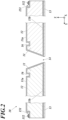
- FIG. 2 is a cross-sectional view showing the configuration of the nozzle plate 10.
- FIG. 2 shows an enlarged cross-sectional view of the nozzle plate 10.
- the nozzle plate 10 consists of a substrate 11 cut from a base material and provided with nozzles 14, a protective film 12 provided on the plate surface of the substrate 11 and the inner wall surfaces of the nozzles 14, a water repellent film 13 formed on the underside of substrate 11 to be overlaid on the protective film 12, a step 151 that is a cut provided at the edge, and glue guards 16 provided on both sides of each nozzle 14.
- the upper side surface of the substrate 11 is referred to as the first surface 11a
- the lower side surface of the substrate 11 is referred to as the second surface 11b.
- the substrate 11 is a plate-shaped member cut from a base material such as SUS (Steel Use Stainless, stainless steel) with a thickness of approximately 25 ⁇ m to 300 ⁇ m.
- a base material such as SUS (Steel Use Stainless, stainless steel) with a thickness of approximately 25 ⁇ m to 300 ⁇ m.
- SUS Steel Use Stainless, stainless steel
- the nozzle plate 10 can be formed with excellent chemical stability against ink and mechanical friction durability.
- a thermal oxide film may be formed on the outer layer of the substrate 11.
- the nozzle 14 is a cylindrical hole with a circular opening on the second surface 11b of the substrate 11.
- the diameter of opening of the nozzle 14 can be approximately 15 ⁇ m to 30 ⁇ m.
- a material that does not dissolve upon contact with the ink such as silicon carbide (SiC), silicon oxi carbide (SiOC), and silicon oxide ( SiO 2 ), , as well as metal oxide films such as aluminum oxide (Al 2 O 3 ), zirconium oxide (ZrO 2 ), titanium oxide (TiO 2 ), hafnium oxide (HfO 2 ) and tantalum oxide (Ta 2 O 3 ), and metal silicate films containing silicon in metal oxide films (tantalum silicate (TaSiO), etc.) can be used.
- SiC silicon carbide
- SiOC silicon oxi carbide
- SiO 2 silicon oxide
- metal oxide films such as aluminum oxide (Al 2 O 3 ), zirconium oxide (ZrO 2 ), titanium oxide (TiO 2 ), hafnium oxide (HfO 2 ) and tantalum oxide (Ta 2 O 3 ), and metal silicate films containing silicon in metal oxide films (tantalum silicate (TaSiO), etc.
- the thickness of the protective film 12 is not limited, but is desirably, for example, 50 nm to 500 nm.
- the protective film 12 made of such ink-resistant material inhibits the substrate 11 from being eroded by ink (especially, alkaline or acidic ink).
- the protective film 12 may also be used as a base film for the water repellent film 13 described below. Since the ink-resistant protective film 12 is not easily peeled off when it comes into contact with ink, by using the protective film 12 as the base film, it is possible to suppress the peeling of the water repellent film 13 together with the protective film 12 as the base film.
- the water repellent film 13 is formed on top of the protective film 12, and its surface forms the ink ejection surface.
- the water repellent film 13 is a layer provided to have water repellency against ink and to inhibit adhering of ink and foreign matter.
- the water repellent film 13 is formed by vapor deposition of a silane coupling agent having perfluoroxyl groups, using the protective film 12 made of the aforementioned material as the base film.
- the water repellent film 13 has openings through the water repellent film 13 at the positions where the nozzles 14 are formed, and ink ejected from the nozzles 14 is ejected through the openings.
- the step 151 is a cut provided along the periphery of the first surface 11a, and dross 152 generated by laser processing, which will be described later, is attached to the edge.
- the step 151 is a space that prevents the dross 152 from interfering with the bonding of the nozzle plate 10 and the channel substrate 20, the dross 152 being generated when external shaping is performed to the recess 15 of the nozzle plate 10. 152.
- the step 151 is also a space to contain the adhesive that protrudes from the edge surface of the nozzle plate 10 during the bonding of the nozzle plate 10 and the channel substrate 20.
- the depth of the step 151 is not limited, but is preferably 5 ⁇ m to 10 ⁇ m.
- the glue guard 16 is a recessed groove section provided so that it is nearly parallel to the row of nozzles 14.
- one glue guard 16 is provided on each side of the nozzle 14, but the position and number of glue guards are not limited to this.
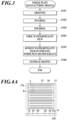
- FIG. 3 is a flowchart showing the procedure of the process for manufacturing the nozzle plate 10 (nozzle plate manufacturing process).
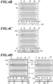
- FIGS. 4A to 4D are top views and cross-sectional views along the A-B line illustrating the nozzle plate manufacturing process.
- multiple nozzle plates 10 can be manufactured simultaneously from a single base material.
- step S106 the portion of the first surface 11a of the substrate 11 that is to be subjected to external shaping in step S106 which is a later process is subjected to grooving (half etching) by a wet etching process to form the recess 15 (Step S101).
- the wet etching process can be performed by forming a resist mask on the substrate 11, excluding the grooving area, and immersing it in the etchant. It is sufficient that the resist mask is able to protect the substrate 11 against the etchant, and the resist mask can be made of inorganic material such as silicon, for example.
- a neutral salt etchant which is an aqueous solution containing ferric chloride (FeCl 2 ), copper chloride (CuCl 2 ) or the like is generally used.
- a neutral salt etchant which is an aqueous solution containing ferric chloride (FeCl 2 ), copper chloride (CuCl 2 ) or the like is generally used.
- a mixture of nitric acid (HNO 3 ) and hydrofluoric acid (HF) is generally used. However, it is not limited to this, and any of the known etchants can be selected.
- the resist mask is removed from the surface of the substrate 11.
- the glue guard 16 which is the concave groove section parallel to the row of nozzles 14 to be formed is formed at the same time.
- Step S102 punching is performed on the substrate 11 to form the nozzles 14 (Step S102).
- the tool is used to press the substrate 11. Specifically, one side of the nozzle forming portion of the tool and the first surface 11a of the substrate 11 are made to face each other, and the nozzle forming portion is pressed against the first surface 11a. As a result, nozzle recesses which are concave toward the second surface 11b are formed on the first surface 11a, and nozzle convex portions are formed on the second surface 11b.
- Step S103 the nozzle convex portions protruding from the second surface 11b are polished and removed. Then, the nozzles 14 are opened on the second surface 11b.
- the substrate 11 has nozzles 14 that penetrate from the first surface 11a to the second surface 11b.
- the protective film 12 is formed on the nozzle plate 10, and the water repellent film 13 is formed on the second surface 11b, which is the ink ejection surface side (Step S104).
- the surface of the substrate 11 is cleaned to remove foreign matter adhering to the substrate 11.
- the method of cleaning the substrate 11 can be, for example, US cleaning.
- Ion bombardment treatment is a treatment in which physical effects are exerted on the material to be treated by bombarding the material to be treated with ions in a reduced pressure environment.
- This ion bombardment treatment removes impurities and thin oxide films from the surface of the substrate 11 to clean it and improve the adhesion property of the protective film 12. In addition, oxidation of the surface of the substrate 11 is suppressed.
- the protective film 12 is formed on the surface of the substrate 11 by the plasma CVD method, and the substrate 11 having the protective film 12 is cleaned to remove foreign matter adhering to the protective film 12.
- the method of cleaning the protective film 12 can be US cleaning as described above.
- the water repellent film 13 is formed on the protective film 12.
- the water repellent film 13 is formed by a dry process, such as vacuum evaporation, using a silane coupling agent having perfluoroxyl groups, for example.
- amino silane coupling agents such as ⁇ -aminopropyltriethoxysilane, N- ⁇ -aminoethyl- ⁇ -aminopropyltriethoxysilane, N- ⁇ -aminoethyl- ⁇ -aminopropyltrimethoxysilane, N- ⁇ -aminoethyl- ⁇ -aminopropylmethyldimethoxysilane, N-phenyl- ⁇ -aminopropyltrimethoxysilane, and ⁇ -ureidopropyltriethoxysilane, and epoxysilane coupling agents such as ⁇ -glycidoxypropyltrimethoxysilane, ⁇ -(3,4-epoxycyclohexyl)ethyl trimethoxysilane, and ⁇ -glycidoxypropyl methyl diethoxysilane are applicable.
- the method of forming the water repellent film 13 is not limited to this.
- the water repellent film 13 may be formed on the basis of conventionally known components and methods, for example, by immersing the substrate 11 in a solution of a fluorine-containing organosilicon compound diluted with a fluorinated solvent and then thermally drying it.
- Step S105 the water repellent film 13 formed on surfaces other than the second surface 1 1b is removed. Specifically, first, the second surface 11b is masked with polyimide tape and the substrate 11 is installed in an ashing machine. Exposure to O 2 plasma is made for several tens of seconds to remove the water repellent film 13 formed on the surfaces other than the second surface 11b. The polyimide tape is then removed and cleaned.
- the protective film 12 is formed on the entire surface of the substrate 11, and the water repellent film 13 is formed only on the second surface 11b.
- external shaping is performed on the substrate 11 by laser processing (external shaping process, step S106).
- the nozzle plate 10 is cut out from the base material by performing the laser processing with the laser equipment along the recess 15 of the substrate 11 on which the grooving was performed in step S101 which is a previous process, and by cutting the recess 15.
- excimer laser light can be preferably used as the laser light generated by the laser equipment. This is because excimer laser light has a short wavelength and is capable of desirable microprocessing. The wavelength of excimer laser light ranges from 190 nm to 355 nm.
- ArF wavelength of 193 nm
- XeCl wavelength of 308 nm
- XeF wavelength of 351 nm
- Conventional known laser beams such as YAG laser, CO 2 laser, and the like may be used as laser beams.
- the step 151 as shown in FIG. 2 is formed at the edge of the nozzle plate 10 after the external shaping process.
- the dross 152 is formed near the processed portion.
- laser processing is performed along the recess 15, and thus the dross 152 is formed at the edge of the step 151 as shown in FIG. 2 .
- the nozzle plate 10 having the step 151 with the dross 152 formed on the edge of the substrate 11 is obtained.
- the head chip 2 is manufactured by stacking the nozzle plate 10 and the channel substrates 20, 40, and 50, and is combined with the common ink chamber 70, the support substrate 80, the wiring member 3, and the drive section 4 to be incorporated into a predetermined exterior member. Thereby, the inkjet head 1 is completed.
- SUS304HTA material with a thickness of 50 ⁇ m was used as the base material, and a solid-state laser system using YVO4 crystals, MD-U1000C (manufactured by Keyence Corporation, wavelength: 355 nm, pulse width: 14 nsec, switch: 40 kHz, scan speed: 200 mm/sec) was used to perform laser processing by 20 scans at a time for each level of laser output (2.4 W / 1.8 W / 1.2 W / 0.6W) with or without assist gas. Next, 20 minutes of US cleaning was performed in pure water using 40 kHz ultrasonic waves. After the US cleaning, a laser microscope, VK-X250 (manufactured by Keyence Corporation) was used to measure the height of the dross 152 generated near the processed portion, and the average value was calculated.
- a laser microscope, VK-X250 manufactured by Keyence Corporation
- Table I is a table showing the results of this experiment.
- the height of the dross 152 can be reduced.
- levels 4 and 8 if the output is reduced to 0.6 W or lower, it is not preferable because it is no longer possible to perform the external shaping.
- the use of an assist gas can reduce the change in the height of the dross 152 due to changes in laser output, and the height can be stabilized at 5 ⁇ m or less.
- the height of dross 152 generated during laser processing is approximately 5 ⁇ m, especially 10 ⁇ m or less. Therefore, if the depth of the step 151 is approximately 5 ⁇ m, the dross 152 is less likely to cause bonding defects or void generation when bonding to the pressure chamber substrate 20. If the depth of the step 151 is approximately 10 ⁇ m, the dross 152 can be prevented from becoming an obstacle to bonding after external shaping, regardless of the conditions at the time of laser processing.
- the method for manufacturing the nozzle plate 10 at least includes a grooving process that is forming multiple recesses 15 in a single substrate by grooving in the wet etching on the portion to be subjected to the external shaping, a nozzle forming process that is forming multiple nozzles 14 by punching and polishing, and an external shaping process that is performing external shaping of the multiple nozzle plates 10 along the recesses 15 by laser processing.
- the dross 152 generated by the external shaping process is generated in the step 151 formed by the grooving process. Therefore, when the nozzle plate 10 is bonded to the pressure chamber substrate 20, the occurrence of defects such as bonding defects and void generation can be suppressed.
- the nozzle plate 10 in the method for manufacturing the nozzle plate 10 according to the embodiment, it is not necessary to remove the dross 152 generated at the edge of the nozzle plate 10 by polishing in order to suppress the occurrence of the aforementioned defects. Therefore, the nozzle plate 10 can be manufactured efficiently and the productivity is excellent.
- each process can be performed to produce multiple nozzle plates 10 from a single substrate 11. Therefore, multiple nozzle plates 10 can be efficiently manufactured, and the productivity is excellent.
- the nozzle plate 10 can be manufactured efficiently and the productivity is excellent.
- the nozzle plate 10 can be provided at a low cost without the need to use a short pulse laser device with a pulse width of picoseconds or femtosecond order.
- the nozzle plate 10 manufactured by the manufacturing method according to the embodiment has the dross 152 at the step 151. Therefore, in bonding with the pressure chamber substrate 20, which is the upper layer substrate, with the adhesive, even if the amount of adhesive is large, it is possible to prevent the dross 152 from becoming a wall to make it protrude to the sides.
- the inkjet head 1 can be manufactured inexpensively and efficiently, and the productivity is excellent.
- the present invention is not limited to the embodiment, but can be modified in various ways.
- the base material of the nozzle plate 10 is made of SUS, but the base material of the nozzle plate 10 is not limited to this.
- other conventionally known materials such as a silicon substrate or electroformed metal such as Ni may be used.
- the protective film 12 may be provided on at least a portion of the first surface 11a and the inner wall surface of nozzle 14 in the surface of the substrate 11 (that is, any range which ink may come into contact with and requires the ink resistance).
- the protective film 12 is a monolayer structure, the composition of the protective film 12 is not limited to this, and a multilayer structure is also acceptable. If the protective film 12 is unnecessary, the nozzle plate 10 does not need to be provided with the protective film 12.
- the inner wall surface of the nozzle 14 may be tapered so that the closer it is to the opening of the nozzle 14, the smaller the cross-sectional area parallel to the first surface 11a is.
- the nozzle 14 in the nozzle plate 10 may include a connecting passageway having an opening wider than the nozzle 14, an ink channel leading ink that is discharged without being ejected from the nozzle 14, or the like.
- the shape of the nozzle 14 is not limited to the abbreviated conical shape as shown in FIG. 2 .
- the nozzle plate 10 does not necessarily need to be provided with the water repellent film 13.
- the embodiment illustrates, as an example, the inkjet head 1 in the vent mode that fluctuates the pressure of ink in the pressure chamber 21 by deforming the piezoelectric element 60 and causes ink to be ejected.
- the present invention may be applied to the inkjet head in the shear mode, in which a pressure chamber is provided inside the piezoelectric body and the pressure of ink in the pressure chamber is fluctuated by generating the shear mode type displacement in the piezoelectric body on the wall of the pressure chamber.
- the present invention is not limited to the method of deforming the pressure chamber.
- the present invention may also be applied to the inkjet head of the thermal method which ejects ink by generating bubbles in the ink by heating.
- the recess 15 is formed by wet etching.
- the processing to form the recess 15 is not limited to this, and the recess 15 may be formed by laser processing.
- the present invention is applicable to the nozzle plate to prevent bonding defects or voids during bonding.
Landscapes
- Engineering & Computer Science (AREA)
- Manufacturing & Machinery (AREA)
- Physics & Mathematics (AREA)
- Optics & Photonics (AREA)
- Particle Formation And Scattering Control In Inkjet Printers (AREA)
Abstract
Description
- The present invention relates to a nozzle plate, an inkjet head, a nozzle plate manufacturing method, and an inkjet head manufacturing method.
- The inkjet head, which ejects ink, consists of the nozzle plate, which is a base material with a nozzle formed on it, to which a channel base material is bonded with an adhesive, and ink is ejected from the nozzle. As a method of forming the nozzle on the base material, a tool is pressed into the base material and squeezed so that the concave portion reaches the back surface of the base material, and then the convex portion on the back surface of the base material is polished to transfer the shape of the tool so that it penetrates the base material (see, for example, Patent Document 1).
- SUS (Steel Use Stainless, stainless steel) and other metals are used as the base material of the nozzle plate from the viewpoints of chemical stability against ink and durability against mechanical friction. Wet etching with an etching solution (see Patent Document 2) and laser etching with a laser device (see Patent Document 3) are known as methods for processing the nozzle plate external shape from the metal plate on which the nozzle is formed.
-
- Patent Document 1:
JP 3755332 B2 - Patent Document 2:
JP 2019-217706 A - Patent Document 3:
JP 2007-307842 A - However, when wet etching is used to perform external shaping, the resist mask may penetrate into the nozzle, and resist residue may remain in the nozzle even after the resist is peeled off after the external shaping.
- Furthermore, when external shaping is performed by laser etching, bonding defects or voids may occur near the laser processing position due to convexity caused by dross. Although the generation of dross can be suppressed by using a short-pulse laser such as picosecond or fetom-second lasers as the laser equipment, the cost of the equipment is higher than that of the nanosecond pulse laser equipment commonly used, making it less economical.
- In addition, when bonding the channel base material to the nozzle plate, there is a risk of adhesive defects where the adhesive protrudes to the sides.
- The present invention was made in view of these circumstances, and its purpose is to provide a nozzle plate, an inkjet head, a nozzle plate manufacturing method, and an inkjet head manufacturing method that can suppress bonding defects or voids during bonding.
- In order to solve the above problem, the invention as recited in
claim 1 is a nozzle plate of an inkjet head, the nozzle plate including: a first surface that is bonded to an upper layer substrate by an adhesive; and a second surface in which an opening of a nozzle that ejects an ink is provided, wherein a step is formed at an edge of the first surface. - The invention as recited in
claim 2 is the nozzle plate according toclaim 1, wherein a dross is attached to the step. - The invention as recited in
claim 3 is the nozzle plate according toclaim - The invention as recited in
claim 4 is the nozzle plate according to any one ofclaims 1 to 3, wherein the step has a depth of 5 µm to 10 µm inclusive, in a center direction of the nozzle plate. - The invention as recited in claim 5 is an inkjet head including the nozzle plate according to any one of
claims 1 to 4. - The invention as recited in claim 6 is a nozzle plate manufacturing method for the nozzle plate according to any one of
claims 1 to 4, the nozzle plate manufacturing method including: a grooving process that is forming a recess in the first surface so as to form external shapes of multiple nozzle plates for a single base material; a nozzle forming process that is forming the nozzle such that the opening is formed in the second surface of the base material; and an external shaping process that is cutting the recess by laser processing and cutting out the nozzle plates from the base material. - The invention as recited in claim 7 is the nozzle plate manufacturing method according to claim 6, wherein the recess is formed by wet etching.
- The invention as recited in claim 8 is the nozzle plate manufacturing method according to claim 6 or 7, further including a water repellent film forming process that is forming a water repellent film in the second surface.
- The invention as recited in claim 9 is an inkjet head manufacturing method including: a nozzle plate manufacturing process that is manufacturing the nozzle plate according to any one of
claims 1 to 4; and a bonding process that is bonding the first surface of the nozzle plate to the upper layer substrate by the adhesive. - According to the nozzle plate, the inkjet head including the nozzle plate, the nozzle plate manufacturing method, and the inkjet head manufacturing method of the present invention, it is possible to suppress the occurrence of bonding defects or voids during bonding.
-
-
FIG. 1A is an overall view of the inkjet head according to the embodiment. -
FIG. 1B is a cross-sectional view along the IB-IB line ofFIG. 1A . -
FIG. 2 is an enlarged cross-sectional view of the nozzle plate according to the embodiment. -
FIG. 3 is a flowchart showing the nozzle plate manufacturing method according to the embodiment. -
FIG. 4A is a top view and a cross-sectional view along the A-B line showing the nozzle plate manufacturing method according to the embodiment. -
FIG. 4B is a top view and a cross-sectional view along the A-B line showing the nozzle plate manufacturing method according to the embodiment. -
FIG. 4C is a top view and a cross-sectional view along the A-B line showing the nozzle plate manufacturing method according to the embodiment. -
FIG. 4D is a top view and a cross-sectional view along the A-B line showing the nozzle plate manufacturing method according to the embodiment. - Hereinafter, embodiments of the nozzle plate, the inkjet head including the nozzle plate, the nozzle plate manufacturing method, and the inkjet head manufacturing method will be described based on the drawings.
-
FIG. 1A is an overall view of theinkjet head 1 according to the embodiment, andFIG. 1B is a cross-sectional view of theinkjet head 1 ofFIG. 1A viewed from the side (-X direction side) along the IB-IB line.FIG. 1B shows a cross-section of theinkjet head 1 in the surface containing the fournozzles 14 included in four nozzle rows. - The
inkjet head 1 includes ahead chip 2, acommon ink chamber 70, asupport substrate 80, awiring member 3, adrive section 4, and the like. - The
head chip 2 is configured to eject ink from thenozzles 14, and is made up of multiple (in this case, four) board-like substrates that are stacked and formed. The lowest substrate in thehead chip 2 is thenozzle plate 10. Thenozzle plate 10 hasmultiple nozzles 14, and ink can be ejected nearly perpendicularly to the ink ejection surface (the exposed surface of the nozzle plate 10) where the openings of thenozzles 14 are provided. On the opposite side of thenozzle plate 10 from the ink ejection surface, the pressure chamber substrate 20 (chamber plate),spacer substrate 40, andwiring substrate 50 are bonded and stacked by adhesive or the like in order toward the upper direction (+Z direction). In the following, thenozzle plate 10,pressure chamber substrate 20,spacer substrate 40, andwiring substrate 50 are also individually or collectively referred to aschannel substrates - These
channel substrates nozzles 14, and are open on the surface on the exposed side (+Z direction side) of thewiring substrate 50. On the exposed surface of thewiring substrate 50, acommon ink chamber 70 is provided to cover all openings. Thecommon ink chamber 70 has, at the upper section, anink supply portion 70a that supplies ink to the inkchamber forming member 70c and anink discharge portion 70b that discharges ink from the inkchamber forming member 70c. The ink stored in the inkchamber forming member 70c of thecommon ink chamber 70 is supplied to eachnozzle 14 from the opening of thewiring substrate 50. - In the middle of the ink channel, a
pressure chamber 21 is provided. Thepressure chamber 21 is provided through thepressure chamber substrate 20 in the vertical direction (Z direction), and the top surface of thepressure chamber 21 is composed of adiaphragm 30 provided between thepressure chamber substrate 20 and thespacer substrate 40. The pressure change is imparted to the ink in thepressure chamber 21 by the deformation of the diaphragm 30 (pressure chamber 21) due to the displacement (deformation) of thepiezoelectric element 60 in thestorage section 41 which is provided adjacent to thepressure chamber 21 via thediaphragm 30. By an appropriate pressure change being applied to the ink in thepressure chamber 21, the ink in the ink channel is ejected as a droplet from thenozzle 14 that is connected to thepressure chamber 21. - The
support substrate 80 is bonded to the top surface of thehead chip 2 and holds the inkchamber forming member 70c of thecommon ink chamber 70. Thesupport substrate 80 is provided with the opening of approximately the same size and shape as the opening on the bottom surface of the inkchamber forming member 70c. The ink in thecommon ink chamber 70 is supplied to the top surface of thehead chip 2 through the opening in the bottom surface of the inkchamber forming member 70c and the opening in thesupport substrate 80. - The
wiring member 3 is, for example, an FPC (Flexible Printed Circuits), or the like, and is connected to the wiring of thewiring substrate 50. Thepiezoelectric element 60 is displaced by the drive signal transmitted to thewiring 51 and the connection 52 (conductive member) in thestorage section 41 via this wiring. Thewiring member 3 is drawn through thesupport substrate 80 and connected to thedrive section 4. - The
drive section 4 receives control signals from the control section of the inkjet recording device and power supply from the power supply section. Thedrive section 4 outputs appropriate drive signals of thepiezoelectric element 60 to thewiring member 3 according to the ink ejection or non-ejection operation from eachnozzle 14. Thedrive section 4 is composed of an IC (Integrated Circuit) or the like. -
FIG. 2 is a cross-sectional view showing the configuration of thenozzle plate 10.FIG. 2 shows an enlarged cross-sectional view of thenozzle plate 10. - The
nozzle plate 10 consists of asubstrate 11 cut from a base material and provided withnozzles 14, aprotective film 12 provided on the plate surface of thesubstrate 11 and the inner wall surfaces of thenozzles 14, awater repellent film 13 formed on the underside ofsubstrate 11 to be overlaid on theprotective film 12, astep 151 that is a cut provided at the edge, andglue guards 16 provided on both sides of eachnozzle 14. - In the following, the upper side surface of the
substrate 11 is referred to as thefirst surface 11a, the lower side surface of thesubstrate 11 is referred to as thesecond surface 11b. - The
substrate 11 is a plate-shaped member cut from a base material such as SUS (Steel Use Stainless, stainless steel) with a thickness of approximately 25 µm to 300 µm. By using SUS as the base material, thenozzle plate 10 can be formed with excellent chemical stability against ink and mechanical friction durability. As described below, when a silicon substrate is used as thesubstrate 11, a thermal oxide film may be formed on the outer layer of thesubstrate 11. - The
nozzle 14 is a cylindrical hole with a circular opening on thesecond surface 11b of thesubstrate 11. - The diameter of opening of the
nozzle 14 can be approximately 15 µm to 30 µm. - For the
protective film 12, a material that does not dissolve upon contact with the ink, such as silicon carbide (SiC), silicon oxi carbide (SiOC), and silicon oxide ( SiO2), , as well as metal oxide films such as aluminum oxide (Al2O3), zirconium oxide (ZrO2), titanium oxide (TiO2), hafnium oxide (HfO2) and tantalum oxide (Ta2O3), and metal silicate films containing silicon in metal oxide films (tantalum silicate (TaSiO), etc.) can be used. - The thickness of the
protective film 12 is not limited, but is desirably, for example, 50 nm to 500 nm. - The
protective film 12 made of such ink-resistant material inhibits thesubstrate 11 from being eroded by ink (especially, alkaline or acidic ink). Theprotective film 12 may also be used as a base film for thewater repellent film 13 described below. Since the ink-resistantprotective film 12 is not easily peeled off when it comes into contact with ink, by using theprotective film 12 as the base film, it is possible to suppress the peeling of thewater repellent film 13 together with theprotective film 12 as the base film. - The
water repellent film 13 is formed on top of theprotective film 12, and its surface forms the ink ejection surface. Thewater repellent film 13 is a layer provided to have water repellency against ink and to inhibit adhering of ink and foreign matter. As thewater repellent film 13, thewater repellent film 13 is formed by vapor deposition of a silane coupling agent having perfluoroxyl groups, using theprotective film 12 made of the aforementioned material as the base film. - The
water repellent film 13 has openings through thewater repellent film 13 at the positions where thenozzles 14 are formed, and ink ejected from thenozzles 14 is ejected through the openings. - The
step 151 is a cut provided along the periphery of thefirst surface 11a, anddross 152 generated by laser processing, which will be described later, is attached to the edge. Thestep 151 is a space that prevents thedross 152 from interfering with the bonding of thenozzle plate 10 and thechannel substrate 20, thedross 152 being generated when external shaping is performed to therecess 15 of thenozzle plate 10. 152. Thestep 151 is also a space to contain the adhesive that protrudes from the edge surface of thenozzle plate 10 during the bonding of thenozzle plate 10 and thechannel substrate 20. - The depth of the
step 151 is not limited, but is preferably 5 µm to 10 µm. - The
glue guard 16 is a recessed groove section provided so that it is nearly parallel to the row ofnozzles 14. By providing theglue guard 16, when thenozzle plate 10 is bonded to thepressure chamber substrate 20, which is the upper layer substrate, with adhesive, there is less risk of excess adhesive getting into thenozzle 14. - In
FIG. 2 , oneglue guard 16 is provided on each side of thenozzle 14, but the position and number of glue guards are not limited to this. - Next, the manufacturing method of the
inkjet head 1 of the embodiment is described, focusing on the manufacturing method of thenozzle plate 10. -
FIG. 3 is a flowchart showing the procedure of the process for manufacturing the nozzle plate 10 (nozzle plate manufacturing process).FIGS. 4A to 4D are top views and cross-sectional views along the A-B line illustrating the nozzle plate manufacturing process. - As shown in
FIG. 4A to FIG. 4D , according to the nozzle plate manufacturing process for the embodiment,multiple nozzle plates 10 can be manufactured simultaneously from a single base material. - In the nozzle plate manufacturing process, first, as shown in
FIG. 4A , the portion of thefirst surface 11a of thesubstrate 11 that is to be subjected to external shaping in step S106 which is a later process is subjected to grooving (half etching) by a wet etching process to form the recess 15 (Step S101). - The wet etching process can be performed by forming a resist mask on the
substrate 11, excluding the grooving area, and immersing it in the etchant. It is sufficient that the resist mask is able to protect thesubstrate 11 against the etchant, and the resist mask can be made of inorganic material such as silicon, for example. As an etchant, for example, if thesubstrate 11 is a SUS base material, a neutral salt etchant, which is an aqueous solution containing ferric chloride (FeCl2), copper chloride (CuCl2) or the like is generally used. When thesubstrate 11 is a silicon substrate, a mixture of nitric acid (HNO3) and hydrofluoric acid (HF) is generally used. However, it is not limited to this, and any of the known etchants can be selected. - After the wet etching process, the resist mask is removed from the surface of the
substrate 11. - In the grooving process, the
glue guard 16 which is the concave groove section parallel to the row ofnozzles 14 to be formed is formed at the same time. - Next, as shown in
FIG. 4B , punching is performed on thesubstrate 11 to form the nozzles 14 (Step S102). - As the punching, the tool is used to press the
substrate 11. Specifically, one side of the nozzle forming portion of the tool and thefirst surface 11a of thesubstrate 11 are made to face each other, and the nozzle forming portion is pressed against thefirst surface 11a. As a result, nozzle recesses which are concave toward thesecond surface 11b are formed on thefirst surface 11a, and nozzle convex portions are formed on thesecond surface 11b. - Next, the nozzle convex portions protruding from the
second surface 11b are polished and removed (Step S103). Then, thenozzles 14 are opened on thesecond surface 11b. - As a result, the
substrate 11 hasnozzles 14 that penetrate from thefirst surface 11a to thesecond surface 11b. - Next, the
protective film 12 is formed on thenozzle plate 10, and thewater repellent film 13 is formed on thesecond surface 11b, which is the ink ejection surface side (Step S104). - First, the surface of the
substrate 11 is cleaned to remove foreign matter adhering to thesubstrate 11. The method of cleaning thesubstrate 11 can be, for example, US cleaning. - After cleaning the
substrate 11, an ion bombardment treatment is performed on the surface of thesubstrate 11. Ion bombardment treatment is a treatment in which physical effects are exerted on the material to be treated by bombarding the material to be treated with ions in a reduced pressure environment. - This ion bombardment treatment removes impurities and thin oxide films from the surface of the
substrate 11 to clean it and improve the adhesion property of theprotective film 12. In addition, oxidation of the surface of thesubstrate 11 is suppressed. - After ion bombardment treatment, the
protective film 12 is formed on the surface of thesubstrate 11 by the plasma CVD method, and thesubstrate 11 having theprotective film 12 is cleaned to remove foreign matter adhering to theprotective film 12. The method of cleaning theprotective film 12 can be US cleaning as described above. - After cleaning the
protective film 12, as shown inFIG. 4C , thewater repellent film 13 is formed on theprotective film 12. Thewater repellent film 13 is formed by a dry process, such as vacuum evaporation, using a silane coupling agent having perfluoroxyl groups, for example. As the silane coupling agents, amino silane coupling agents such as γ-aminopropyltriethoxysilane, N-β-aminoethyl-γ-aminopropyltriethoxysilane, N-β-aminoethyl-γ-aminopropyltrimethoxysilane, N-β-aminoethyl-γ-aminopropylmethyldimethoxysilane, N-phenyl-γ-aminopropyltrimethoxysilane, and γ-ureidopropyltriethoxysilane, and epoxysilane coupling agents such as γ-glycidoxypropyltrimethoxysilane, β-(3,4-epoxycyclohexyl)ethyl trimethoxysilane, and γ-glycidoxypropyl methyl diethoxysilane are applicable. - The method of forming the
water repellent film 13 is not limited to this. Thewater repellent film 13 may be formed on the basis of conventionally known components and methods, for example, by immersing thesubstrate 11 in a solution of a fluorine-containing organosilicon compound diluted with a fluorinated solvent and then thermally drying it. - Next, the
water repellent film 13 formed on surfaces other than thesecond surface 1 1b is removed (Step S105). Specifically, first, thesecond surface 11b is masked with polyimide tape and thesubstrate 11 is installed in an ashing machine. Exposure to O2 plasma is made for several tens of seconds to remove thewater repellent film 13 formed on the surfaces other than thesecond surface 11b. The polyimide tape is then removed and cleaned. - By the method described above, the
protective film 12 is formed on the entire surface of thesubstrate 11, and thewater repellent film 13 is formed only on thesecond surface 11b. - Next, as shown in
FIG. 4D , external shaping is performed on thesubstrate 11 by laser processing (external shaping process, step S106). - In the external shaping process, the
nozzle plate 10 is cut out from the base material by performing the laser processing with the laser equipment along therecess 15 of thesubstrate 11 on which the grooving was performed in step S101 which is a previous process, and by cutting therecess 15. For example, excimer laser light can be preferably used as the laser light generated by the laser equipment. This is because excimer laser light has a short wavelength and is capable of desirable microprocessing. The wavelength of excimer laser light ranges from 190 nm to 355 nm. Specifically, for example, ArF (wavelength of 193 nm), KrF (248 nm), XeCl (wavelength of 308 nm), XeF (wavelength of 351 nm), and the like are preferably cited. Conventional known laser beams such as YAG laser, CO2 laser, and the like may be used as laser beams. - Since the laser processing in this process is performed by cutting the
recess 15 of thenozzle plate 10 as described above, thestep 151 as shown inFIG. 2 is formed at the edge of thenozzle plate 10 after the external shaping process. - In addition, when the external shaping is performed on the
substrate 11 which is SUS by laser processing, in general, thedross 152 is formed near the processed portion. However, in the present invention, laser processing is performed along therecess 15, and thus thedross 152 is formed at the edge of thestep 151 as shown inFIG. 2 . - By the method described above, the
nozzle plate 10 having thestep 151 with thedross 152 formed on the edge of thesubstrate 11 is obtained. Thehead chip 2 is manufactured by stacking thenozzle plate 10 and thechannel substrates common ink chamber 70, thesupport substrate 80, thewiring member 3, and thedrive section 4 to be incorporated into a predetermined exterior member. Thereby, theinkjet head 1 is completed. - Next, the experiment conducted to confirm the height of the dross formed by the external shaping in the embodiment will be explained.
- In this experiment, the height of the
dross 152 formed when SUS is laser processed was evaluated. - Specifically, SUS304HTA material with a thickness of 50 µm was used as the base material, and a solid-state laser system using YVO4 crystals, MD-U1000C (manufactured by Keyence Corporation, wavelength: 355 nm, pulse width: 14 nsec, switch: 40 kHz, scan speed: 200 mm/sec) was used to perform laser processing by 20 scans at a time for each level of laser output (2.4 W / 1.8 W / 1.2 W / 0.6W) with or without assist gas. Next, 20 minutes of US cleaning was performed in pure water using 40 kHz ultrasonic waves. After the US cleaning, a laser microscope, VK-X250 (manufactured by Keyence Corporation) was used to measure the height of the
dross 152 generated near the processed portion, and the average value was calculated. - Table I is a table showing the results of this experiment.
-
Table I LEVEL 1 2 3 4 5 6 7 8 ASSIST GAS NOT USE NOT USE NOT USE NOT USE USE USE USE USE OUTPUT (W) 2.4 1.8 1.2 0.6 2.4 1.8 1.2 0.6 DROSS HEIGHT (µm) 7.6 5.7 3.9 - (PROCESSING NOT POSSIBLE) 3.9 4.2 4.3 - (PROCESSING NOT POSSIBLE) - As shown in
levels 1 to 3 of Table 1, as the laser output is reduced, the height of thedross 152 can be reduced. However, as shown inlevels 4 and 8, if the output is reduced to 0.6 W or lower, it is not preferable because it is no longer possible to perform the external shaping. - In addition, as shown in levels 5 to 7, the use of an assist gas can reduce the change in the height of the
dross 152 due to changes in laser output, and the height can be stabilized at 5 µm or less. - As shown in
Experiment 1, the height ofdross 152 generated during laser processing is approximately 5 µm, especially 10 µm or less. Therefore, if the depth of thestep 151 is approximately 5 µm, thedross 152 is less likely to cause bonding defects or void generation when bonding to thepressure chamber substrate 20. If the depth of thestep 151 is approximately 10 µm, thedross 152 can be prevented from becoming an obstacle to bonding after external shaping, regardless of the conditions at the time of laser processing. - As described above, the method for manufacturing the
nozzle plate 10 according to the embodiment at least includes a grooving process that is formingmultiple recesses 15 in a single substrate by grooving in the wet etching on the portion to be subjected to the external shaping, a nozzle forming process that is formingmultiple nozzles 14 by punching and polishing, and an external shaping process that is performing external shaping of themultiple nozzle plates 10 along therecesses 15 by laser processing. - According to such a method, the
dross 152 generated by the external shaping process is generated in thestep 151 formed by the grooving process. Therefore, when thenozzle plate 10 is bonded to thepressure chamber substrate 20, the occurrence of defects such as bonding defects and void generation can be suppressed. - In addition, in the method for manufacturing the
nozzle plate 10 according to the embodiment, it is not necessary to remove thedross 152 generated at the edge of thenozzle plate 10 by polishing in order to suppress the occurrence of the aforementioned defects. Therefore, thenozzle plate 10 can be manufactured efficiently and the productivity is excellent. - In addition, in the method for manufacturing the
nozzle plate 10 according to the embodiment, as shown inFIG. 4 , each process can be performed to producemultiple nozzle plates 10 from asingle substrate 11. Therefore,multiple nozzle plates 10 can be efficiently manufactured, and the productivity is excellent. - In addition, in the method for manufacturing the
nozzle plate 10 according to the embodiment, since the external shaping is performed by laser processing, compared to the case where the external shaping is performed by wet etching, the process of forming and removing the resist mask becomes unnecessary, and resist residue inside thenozzle 14 is not generated. Therefore, thenozzle plate 10 can be manufactured efficiently and the productivity is excellent. - In addition, in the method for manufacturing the
nozzle plate 10 according to the embodiment, even if thedross 152 is generated during the external shaping process, the occurrence of the aforementioned defects can be suppressed. Therefore, thenozzle plate 10 can be provided at a low cost without the need to use a short pulse laser device with a pulse width of picoseconds or femtosecond order. - In addition, the
nozzle plate 10 manufactured by the manufacturing method according to the embodiment has thedross 152 at thestep 151. Therefore, in bonding with thepressure chamber substrate 20, which is the upper layer substrate, with the adhesive, even if the amount of adhesive is large, it is possible to prevent thedross 152 from becoming a wall to make it protrude to the sides. - In addition, by using the
nozzle plate 10 manufactured by the manufacturing method according to the embodiment, theinkjet head 1 can be manufactured inexpensively and efficiently, and the productivity is excellent. - The present invention is not limited to the embodiment, but can be modified in various ways.
- For example, in the embodiment, the base material of the
nozzle plate 10 is made of SUS, but the base material of thenozzle plate 10 is not limited to this. For example, other conventionally known materials such as a silicon substrate or electroformed metal such as Ni may be used. - In the embodiment, an example of forming the
protective film 12 on the entire surface of thesubstrate 11 is used, but the range of forming theprotective film 12 is not limited to this. Theprotective film 12 may be provided on at least a portion of thefirst surface 11a and the inner wall surface ofnozzle 14 in the surface of the substrate 11 (that is, any range which ink may come into contact with and requires the ink resistance). - Although the
protective film 12 is a monolayer structure, the composition of theprotective film 12 is not limited to this, and a multilayer structure is also acceptable. If theprotective film 12 is unnecessary, thenozzle plate 10 does not need to be provided with theprotective film 12. - The inner wall surface of the
nozzle 14 may be tapered so that the closer it is to the opening of thenozzle 14, the smaller the cross-sectional area parallel to thefirst surface 11a is. - The
nozzle 14 in thenozzle plate 10 may include a connecting passageway having an opening wider than thenozzle 14, an ink channel leading ink that is discharged without being ejected from thenozzle 14, or the like. The shape of thenozzle 14 is not limited to the abbreviated conical shape as shown inFIG. 2 . - In cases where the
inkjet head 1 does not need to have the water repellency in the ink ejection surface, thenozzle plate 10 does not necessarily need to be provided with thewater repellent film 13. - The embodiment illustrates, as an example, the
inkjet head 1 in the vent mode that fluctuates the pressure of ink in thepressure chamber 21 by deforming thepiezoelectric element 60 and causes ink to be ejected. However, this is not intended to be a limitation. For example, the present invention may be applied to the inkjet head in the shear mode, in which a pressure chamber is provided inside the piezoelectric body and the pressure of ink in the pressure chamber is fluctuated by generating the shear mode type displacement in the piezoelectric body on the wall of the pressure chamber. The present invention is not limited to the method of deforming the pressure chamber. For example, the present invention may also be applied to the inkjet head of the thermal method which ejects ink by generating bubbles in the ink by heating. - In the embodiment, in the grooving process, the
recess 15 is formed by wet etching. However, the processing to form therecess 15 is not limited to this, and therecess 15 may be formed by laser processing. However, it is preferable to form therecess 15 by wet etching since laser processing may cause distortion and warping of the base material. - Although some embodiments of the present invention have been described, the scope of the present invention is not limited to the embodiments described above, but includes the scope of the invention as described in the claims and their equivalents.
- The present invention is applicable to the nozzle plate to prevent bonding defects or voids during bonding.
-
- 1 inkjet head
- 10 nozzle plate
- 11a first surface
- 11b second surface
- 13 water repellent film
- 14 nozzle
- 15 recess
- 20 pressure chamber substrate (upper layer substrate)
- 151 step
- 152 dross
Claims (9)
- A nozzle plate of an inkjet head, the nozzle plate comprising:a first surface that is bonded to an upper layer substrate by an adhesive; anda second surface in which an opening of a nozzle that ejects an ink is provided, whereina step is formed at an edge of the first surface.
- The nozzle plate according to claim 1, wherein a dross is attached to the step.
- The nozzle plate according to claim 1 or 2, wherein a base material that forms the nozzle plate is silicon or metal.
- The nozzle plate according to any one of claims 1 to 3, wherein the step has a depth of 5 µm to 10 µm inclusive, in a center direction of the nozzle plate.
- An inkjet head comprising the nozzle plate according to any one of claims 1 to 4.
- A nozzle plate manufacturing method for the nozzle plate according to any one of claims 1 to 4, the nozzle plate manufacturing method comprising:a grooving process that is forming a recess in the first surface so as to form external shapes of multiple nozzle plates for a single base material;a nozzle forming process that is forming the nozzle such that the opening is formed in the second surface of the base material; andan external shaping process that is cutting the recess by laser processing and cutting out the nozzle plates from the base material.
- The nozzle plate manufacturing method according to claim 6, wherein the recess is formed by wet etching.
- The nozzle plate manufacturing method according to claim 6 or 7, further comprising a water repellent film forming process that is forming a water repellent film in the second surface.
- An inkjet head manufacturing method comprising:a nozzle plate manufacturing process that is manufacturing the nozzle plate according to any one of claims 1 to 4; anda bonding process that is bonding the first surface of the nozzle plate to the upper layer substrate by the adhesive.
Applications Claiming Priority (2)
| Application Number | Priority Date | Filing Date | Title |
|---|---|---|---|
| JP2020111031 | 2020-06-29 | ||
| PCT/JP2021/023363 WO2022004459A1 (en) | 2020-06-29 | 2021-06-21 | Nozzle plate, inkjet head, nozzle plate manufacturing method, and inkjet head manufacturing method |
Publications (3)
| Publication Number | Publication Date |
|---|---|
| EP4173827A1 true EP4173827A1 (en) | 2023-05-03 |
| EP4173827A4 EP4173827A4 (en) | 2024-01-03 |
| EP4173827B1 EP4173827B1 (en) | 2025-03-26 |
Family
ID=79316158
Family Applications (1)
| Application Number | Title | Priority Date | Filing Date |
|---|---|---|---|
| EP21834473.7A Active EP4173827B1 (en) | 2020-06-29 | 2021-06-21 | Nozzle plate manufacturing method, and inkjet head manufacturing method |
Country Status (5)
| Country | Link |
|---|---|
| US (1) | US12246537B2 (en) |
| EP (1) | EP4173827B1 (en) |
| JP (1) | JP7708103B2 (en) |
| CN (1) | CN115734879B (en) |
| WO (1) | WO2022004459A1 (en) |
Family Cites Families (23)
| Publication number | Priority date | Publication date | Assignee | Title |
|---|---|---|---|---|
| JPH10217485A (en) * | 1997-02-10 | 1998-08-18 | Toshiba Corp | Printhead manufacturing method |
| JP2000246475A (en) | 1999-02-25 | 2000-09-12 | Seiko Epson Corp | Processing method by laser beam |
| JP3755332B2 (en) | 1999-04-08 | 2006-03-15 | コニカミノルタホールディングス株式会社 | Method for forming nozzle for inkjet head |
| US6569343B1 (en) * | 1999-07-02 | 2003-05-27 | Canon Kabushiki Kaisha | Method for producing liquid discharge head, liquid discharge head, head cartridge, liquid discharging recording apparatus, method for producing silicon plate and silicon plate |
| JP2003251811A (en) * | 2002-03-06 | 2003-09-09 | Brother Ind Ltd | Ink jet printer head and method of manufacturing the same |
| JP2005119222A (en) * | 2003-10-20 | 2005-05-12 | Canon Inc | Nozzle plate manufacturing method and inkjet recording apparatus |
| JP4617770B2 (en) * | 2004-08-19 | 2011-01-26 | 富士ゼロックス株式会社 | Method for manufacturing laminated nozzle plate |
| JP4494367B2 (en) | 2006-05-19 | 2010-06-30 | シャープ株式会社 | Nozzle plate manufacturing method |
| JP5008939B2 (en) * | 2006-09-29 | 2012-08-22 | 富士フイルム株式会社 | Nozzle plate manufacturing method, liquid discharge head, and image forming apparatus |
| JP2008284579A (en) * | 2007-05-16 | 2008-11-27 | Fuji Xerox Co Ltd | Manufacturing method of liquid droplet ejection head, and liquid droplet ejection head |
| JP2009160923A (en) * | 2007-12-10 | 2009-07-23 | Seiko Epson Corp | Liquid ejecting head manufacturing method and liquid ejecting apparatus |
| JP2010149375A (en) * | 2008-12-25 | 2010-07-08 | Seiko Epson Corp | Method for manufacturing nozzle substrate, and method for manufacturing liquid droplet delivering head |
| JP2010214895A (en) * | 2009-03-18 | 2010-09-30 | Toshiba Tec Corp | Inkjet head and method for manufacturing inkjet head |
| WO2011151206A1 (en) * | 2010-06-02 | 2011-12-08 | Oce-Technologies B.V. | Method for manufacturing a nozzle and an associated funnel in a single plate |
| JP2014124887A (en) * | 2012-12-27 | 2014-07-07 | Seiko Epson Corp | Liquid jet head and liquid jet device |
| JP2017061115A (en) * | 2015-09-25 | 2017-03-30 | 株式会社リコー | Droplet discharge member, image forming apparatus, and method for forming through hole for plate-like member |
| JP6645113B2 (en) * | 2015-10-16 | 2020-02-12 | 株式会社リコー | Bonding member, liquid discharge head, liquid discharge unit, device for discharging liquid |
| JP6817008B2 (en) * | 2016-09-29 | 2021-01-20 | エスアイアイ・プリンテック株式会社 | Liquid injection head and liquid injection recorder |
| WO2019116532A1 (en) * | 2017-12-15 | 2019-06-20 | コニカミノルタ株式会社 | Ink jet head, ink jet recording apparatus, and ink jet head manufacturing method |
| JP7020543B2 (en) | 2018-04-20 | 2022-02-16 | コニカミノルタ株式会社 | Nozzle plate manufacturing method and inkjet head |
| JP7139710B2 (en) | 2018-06-21 | 2022-09-21 | セイコーエプソン株式会社 | LIQUID EJECTING HEAD AND LIQUID EJECTING APPARATUS |
| JP7155997B2 (en) * | 2018-12-20 | 2022-10-19 | セイコーエプソン株式会社 | Liquid ejecting head and liquid ejecting device |
| JP7413748B2 (en) * | 2019-12-12 | 2024-01-16 | セイコーエプソン株式会社 | Inkjet recording method and inkjet recording device |
-
2021
- 2021-06-21 US US18/001,435 patent/US12246537B2/en active Active
- 2021-06-21 WO PCT/JP2021/023363 patent/WO2022004459A1/en not_active Ceased
- 2021-06-21 JP JP2022533875A patent/JP7708103B2/en active Active
- 2021-06-21 CN CN202180044960.6A patent/CN115734879B/en active Active
- 2021-06-21 EP EP21834473.7A patent/EP4173827B1/en active Active
Also Published As
| Publication number | Publication date |
|---|---|
| US20230234354A1 (en) | 2023-07-27 |
| US12246537B2 (en) | 2025-03-11 |
| JP7708103B2 (en) | 2025-07-15 |
| EP4173827B1 (en) | 2025-03-26 |
| CN115734879A (en) | 2023-03-03 |
| WO2022004459A1 (en) | 2022-01-06 |
| JPWO2022004459A1 (en) | 2022-01-06 |
| CN115734879B (en) | 2026-03-17 |
| EP4173827A4 (en) | 2024-01-03 |
Similar Documents
| Publication | Publication Date | Title |
|---|---|---|
| JP4766658B2 (en) | Liquid discharge head and manufacturing method thereof | |
| US8377828B2 (en) | Method of manufacturing a substrate for a liquid discharge head | |
| JP2013212681A (en) | Method for manufacturing liquid ejection head substrate | |
| US6925712B2 (en) | Method of fabricating a liquid-jet head | |
| JP4979793B2 (en) | Manufacturing method of substrate for liquid discharge head | |
| EP4173827B1 (en) | Nozzle plate manufacturing method, and inkjet head manufacturing method | |
| EP1799461B1 (en) | Methods of fabricating nozzle plates | |
| JP2008149649A (en) | Ink jet head and manufacturing method thereof | |
| JP2007317747A (en) | Substrate dividing method and liquid jet head manufacturing method | |
| US7402256B2 (en) | Method for producing liquid-jet head | |
| JP2012213967A (en) | Method for manufacturing liquid ejection head | |
| CN103862872B (en) | The manufacture method of ink gun and ink gun | |
| JP2009061614A (en) | Ink jet head and method of manufacturing ink jet head | |
| JP2003063014A (en) | Method of manufacturing nozzle plate for inkjet printer | |
| US8460948B2 (en) | Method for manufacturing liquid ejecting head | |
| JP4442486B2 (en) | Method for manufacturing liquid jet head | |
| JP2006224596A (en) | Ink jet recording head and method of manufacturing ink jet recording head | |
| JP4730537B2 (en) | Method for manufacturing liquid jet head | |
| JP4494367B2 (en) | Nozzle plate manufacturing method | |
| JP2011079245A (en) | Nozzle substrate, method for manufacturing nozzle substrate, droplet ejection head and droplet ejection device | |
| JP6991760B2 (en) | How to process a silicon substrate | |
| JP2007168193A (en) | Method for manufacturing ink jet recording head | |
| JP2007245638A (en) | Method for manufacturing ink jet recording head | |
| JP2011083899A (en) | Method for manufacturing passage forming substrate of ink-jet recording head, passage forming substrate, and ink-jet recording head | |
| JP2006175654A (en) | Method for manufacturing liquid jet head and liquid jet head |
Legal Events
| Date | Code | Title | Description |
|---|---|---|---|
| STAA | Information on the status of an ep patent application or granted ep patent |
Free format text: STATUS: THE INTERNATIONAL PUBLICATION HAS BEEN MADE |
|
| PUAI | Public reference made under article 153(3) epc to a published international application that has entered the european phase |
Free format text: ORIGINAL CODE: 0009012 |
|
| STAA | Information on the status of an ep patent application or granted ep patent |
Free format text: STATUS: REQUEST FOR EXAMINATION WAS MADE |
|
| 17P | Request for examination filed |
Effective date: 20221221 |
|
| AK | Designated contracting states |
Kind code of ref document: A1 Designated state(s): AL AT BE BG CH CY CZ DE DK EE ES FI FR GB GR HR HU IE IS IT LI LT LU LV MC MK MT NL NO PL PT RO RS SE SI SK SM TR |
|
| DAV | Request for validation of the european patent (deleted) | ||
| DAX | Request for extension of the european patent (deleted) | ||
| A4 | Supplementary search report drawn up and despatched |
Effective date: 20231130 |
|
| RIC1 | Information provided on ipc code assigned before grant |
Ipc: B41J 2/16 20060101ALI20231124BHEP Ipc: B41J 2/14 20060101AFI20231124BHEP |
|
| GRAP | Despatch of communication of intention to grant a patent |
Free format text: ORIGINAL CODE: EPIDOSNIGR1 |
|
| STAA | Information on the status of an ep patent application or granted ep patent |
Free format text: STATUS: GRANT OF PATENT IS INTENDED |
|
| INTG | Intention to grant announced |
Effective date: 20241125 |
|
| GRAS | Grant fee paid |
Free format text: ORIGINAL CODE: EPIDOSNIGR3 |
|
| GRAA | (expected) grant |
Free format text: ORIGINAL CODE: 0009210 |
|
| STAA | Information on the status of an ep patent application or granted ep patent |
Free format text: STATUS: THE PATENT HAS BEEN GRANTED |
|
| P01 | Opt-out of the competence of the unified patent court (upc) registered |
Free format text: CASE NUMBER: APP_6294/2025 Effective date: 20250206 |
|
| AK | Designated contracting states |
Kind code of ref document: B1 Designated state(s): AL AT BE BG CH CY CZ DE DK EE ES FI FR GB GR HR HU IE IS IT LI LT LU LV MC MK MT NL NO PL PT RO RS SE SI SK SM TR |
|
| REG | Reference to a national code |
Ref country code: GB Ref legal event code: FG4D |
|
| REG | Reference to a national code |
Ref country code: CH Ref legal event code: EP |
|
| REG | Reference to a national code |
Ref country code: DE Ref legal event code: R096 Ref document number: 602021028252 Country of ref document: DE |
|
| REG | Reference to a national code |
Ref country code: IE Ref legal event code: FG4D |
|
| PG25 | Lapsed in a contracting state [announced via postgrant information from national office to epo] |
Ref country code: RS Free format text: LAPSE BECAUSE OF FAILURE TO SUBMIT A TRANSLATION OF THE DESCRIPTION OR TO PAY THE FEE WITHIN THE PRESCRIBED TIME-LIMIT Effective date: 20250626 |
|
| PG25 | Lapsed in a contracting state [announced via postgrant information from national office to epo] |
Ref country code: FI Free format text: LAPSE BECAUSE OF FAILURE TO SUBMIT A TRANSLATION OF THE DESCRIPTION OR TO PAY THE FEE WITHIN THE PRESCRIBED TIME-LIMIT Effective date: 20250326 |
|
| PGFP | Annual fee paid to national office [announced via postgrant information from national office to epo] |
Ref country code: DE Payment date: 20250429 Year of fee payment: 5 |
|
| PGFP | Annual fee paid to national office [announced via postgrant information from national office to epo] |
Ref country code: GB Payment date: 20250501 Year of fee payment: 5 |
|
| REG | Reference to a national code |
Ref country code: LT Ref legal event code: MG9D |
|
| PG25 | Lapsed in a contracting state [announced via postgrant information from national office to epo] |
Ref country code: NO Free format text: LAPSE BECAUSE OF FAILURE TO SUBMIT A TRANSLATION OF THE DESCRIPTION OR TO PAY THE FEE WITHIN THE PRESCRIBED TIME-LIMIT Effective date: 20250626 |
|
| PG25 | Lapsed in a contracting state [announced via postgrant information from national office to epo] |
Ref country code: HR Free format text: LAPSE BECAUSE OF FAILURE TO SUBMIT A TRANSLATION OF THE DESCRIPTION OR TO PAY THE FEE WITHIN THE PRESCRIBED TIME-LIMIT Effective date: 20250326 |
|
| PG25 | Lapsed in a contracting state [announced via postgrant information from national office to epo] |
Ref country code: LV Free format text: LAPSE BECAUSE OF FAILURE TO SUBMIT A TRANSLATION OF THE DESCRIPTION OR TO PAY THE FEE WITHIN THE PRESCRIBED TIME-LIMIT Effective date: 20250326 |
|
| PGFP | Annual fee paid to national office [announced via postgrant information from national office to epo] |
Ref country code: FR Payment date: 20250508 Year of fee payment: 5 |
|
| PG25 | Lapsed in a contracting state [announced via postgrant information from national office to epo] |
Ref country code: BG Free format text: LAPSE BECAUSE OF FAILURE TO SUBMIT A TRANSLATION OF THE DESCRIPTION OR TO PAY THE FEE WITHIN THE PRESCRIBED TIME-LIMIT Effective date: 20250326 Ref country code: GR Free format text: LAPSE BECAUSE OF FAILURE TO SUBMIT A TRANSLATION OF THE DESCRIPTION OR TO PAY THE FEE WITHIN THE PRESCRIBED TIME-LIMIT Effective date: 20250627 |
|
| PGFP | Annual fee paid to national office [announced via postgrant information from national office to epo] |
Ref country code: AT Payment date: 20250721 Year of fee payment: 5 |
|
| REG | Reference to a national code |
Ref country code: NL Ref legal event code: MP Effective date: 20250326 |
|
| PG25 | Lapsed in a contracting state [announced via postgrant information from national office to epo] |
Ref country code: NL Free format text: LAPSE BECAUSE OF FAILURE TO SUBMIT A TRANSLATION OF THE DESCRIPTION OR TO PAY THE FEE WITHIN THE PRESCRIBED TIME-LIMIT Effective date: 20250326 |
|
| PG25 | Lapsed in a contracting state [announced via postgrant information from national office to epo] |
Ref country code: SE Free format text: LAPSE BECAUSE OF FAILURE TO SUBMIT A TRANSLATION OF THE DESCRIPTION OR TO PAY THE FEE WITHIN THE PRESCRIBED TIME-LIMIT Effective date: 20250326 |
|
| REG | Reference to a national code |
Ref country code: AT Ref legal event code: MK05 Ref document number: 1778688 Country of ref document: AT Kind code of ref document: T Effective date: 20250326 |
|
| PG25 | Lapsed in a contracting state [announced via postgrant information from national office to epo] |
Ref country code: SM Free format text: LAPSE BECAUSE OF FAILURE TO SUBMIT A TRANSLATION OF THE DESCRIPTION OR TO PAY THE FEE WITHIN THE PRESCRIBED TIME-LIMIT Effective date: 20250326 |
|
| PG25 | Lapsed in a contracting state [announced via postgrant information from national office to epo] |
Ref country code: ES Free format text: LAPSE BECAUSE OF FAILURE TO SUBMIT A TRANSLATION OF THE DESCRIPTION OR TO PAY THE FEE WITHIN THE PRESCRIBED TIME-LIMIT Effective date: 20250326 Ref country code: PT Free format text: LAPSE BECAUSE OF FAILURE TO SUBMIT A TRANSLATION OF THE DESCRIPTION OR TO PAY THE FEE WITHIN THE PRESCRIBED TIME-LIMIT Effective date: 20250728 |
|
| PG25 | Lapsed in a contracting state [announced via postgrant information from national office to epo] |
Ref country code: IT Free format text: LAPSE BECAUSE OF FAILURE TO SUBMIT A TRANSLATION OF THE DESCRIPTION OR TO PAY THE FEE WITHIN THE PRESCRIBED TIME-LIMIT Effective date: 20250326 Ref country code: PL Free format text: LAPSE BECAUSE OF FAILURE TO SUBMIT A TRANSLATION OF THE DESCRIPTION OR TO PAY THE FEE WITHIN THE PRESCRIBED TIME-LIMIT Effective date: 20250326 |
|
| PG25 | Lapsed in a contracting state [announced via postgrant information from national office to epo] |
Ref country code: AT Free format text: LAPSE BECAUSE OF FAILURE TO SUBMIT A TRANSLATION OF THE DESCRIPTION OR TO PAY THE FEE WITHIN THE PRESCRIBED TIME-LIMIT Effective date: 20250326 |
|
| PG25 | Lapsed in a contracting state [announced via postgrant information from national office to epo] |
Ref country code: EE Free format text: LAPSE BECAUSE OF FAILURE TO SUBMIT A TRANSLATION OF THE DESCRIPTION OR TO PAY THE FEE WITHIN THE PRESCRIBED TIME-LIMIT Effective date: 20250326 |
|
| PG25 | Lapsed in a contracting state [announced via postgrant information from national office to epo] |
Ref country code: RO Free format text: LAPSE BECAUSE OF FAILURE TO SUBMIT A TRANSLATION OF THE DESCRIPTION OR TO PAY THE FEE WITHIN THE PRESCRIBED TIME-LIMIT Effective date: 20250326 |
|
| PG25 | Lapsed in a contracting state [announced via postgrant information from national office to epo] |
Ref country code: SK Free format text: LAPSE BECAUSE OF FAILURE TO SUBMIT A TRANSLATION OF THE DESCRIPTION OR TO PAY THE FEE WITHIN THE PRESCRIBED TIME-LIMIT Effective date: 20250326 |
|
| PG25 | Lapsed in a contracting state [announced via postgrant information from national office to epo] |
Ref country code: IS Free format text: LAPSE BECAUSE OF FAILURE TO SUBMIT A TRANSLATION OF THE DESCRIPTION OR TO PAY THE FEE WITHIN THE PRESCRIBED TIME-LIMIT Effective date: 20250726 |
|
| REG | Reference to a national code |
Ref country code: DE Ref legal event code: R097 Ref document number: 602021028252 Country of ref document: DE |
|
| PG25 | Lapsed in a contracting state [announced via postgrant information from national office to epo] |
Ref country code: DK Free format text: LAPSE BECAUSE OF FAILURE TO SUBMIT A TRANSLATION OF THE DESCRIPTION OR TO PAY THE FEE WITHIN THE PRESCRIBED TIME-LIMIT Effective date: 20250326 |
|
| PG25 | Lapsed in a contracting state [announced via postgrant information from national office to epo] |
Ref country code: CZ Free format text: LAPSE BECAUSE OF FAILURE TO SUBMIT A TRANSLATION OF THE DESCRIPTION OR TO PAY THE FEE WITHIN THE PRESCRIBED TIME-LIMIT Effective date: 20250326 |
|
| REG | Reference to a national code |
Ref country code: CH Ref legal event code: H13 Free format text: ST27 STATUS EVENT CODE: U-0-0-H10-H13 (AS PROVIDED BY THE NATIONAL OFFICE) Effective date: 20260127 |
|
| PG25 | Lapsed in a contracting state [announced via postgrant information from national office to epo] |
Ref country code: MC Free format text: LAPSE BECAUSE OF FAILURE TO SUBMIT A TRANSLATION OF THE DESCRIPTION OR TO PAY THE FEE WITHIN THE PRESCRIBED TIME-LIMIT Effective date: 20250326 |
|
| PLBE | No opposition filed within time limit |
Free format text: ORIGINAL CODE: 0009261 |
|
| STAA | Information on the status of an ep patent application or granted ep patent |
Free format text: STATUS: NO OPPOSITION FILED WITHIN TIME LIMIT |
|
| REG | Reference to a national code |
Ref country code: CH Ref legal event code: L10 Free format text: ST27 STATUS EVENT CODE: U-0-0-L10-L00 (AS PROVIDED BY THE NATIONAL OFFICE) Effective date: 20260211 |
|
| PG25 | Lapsed in a contracting state [announced via postgrant information from national office to epo] |
Ref country code: LU Free format text: LAPSE BECAUSE OF NON-PAYMENT OF DUE FEES Effective date: 20250621 |
|
| REG | Reference to a national code |
Ref country code: BE Ref legal event code: MM Effective date: 20250630 |
|
| 26N | No opposition filed |
Effective date: 20260105 |
|
| PG25 | Lapsed in a contracting state [announced via postgrant information from national office to epo] |
Ref country code: IE Free format text: LAPSE BECAUSE OF NON-PAYMENT OF DUE FEES Effective date: 20250621 |
|
| PG25 | Lapsed in a contracting state [announced via postgrant information from national office to epo] |
Ref country code: BE Free format text: LAPSE BECAUSE OF NON-PAYMENT OF DUE FEES Effective date: 20250630 |
|
| PG25 | Lapsed in a contracting state [announced via postgrant information from national office to epo] |
Ref country code: CH Free format text: LAPSE BECAUSE OF NON-PAYMENT OF DUE FEES Effective date: 20250630 |