EP4171843B1 - Substrate mapping apparatus and method therefor - Google Patents
Substrate mapping apparatus and method therefor Download PDFInfo
- Publication number
- EP4171843B1 EP4171843B1 EP21834134.5A EP21834134A EP4171843B1 EP 4171843 B1 EP4171843 B1 EP 4171843B1 EP 21834134 A EP21834134 A EP 21834134A EP 4171843 B1 EP4171843 B1 EP 4171843B1
- Authority
- EP
- European Patent Office
- Prior art keywords
- substrate
- wafer
- camera
- respective camera
- substrate carrier
- Prior art date
- Legal status (The legal status is an assumption and is not a legal conclusion. Google has not performed a legal analysis and makes no representation as to the accuracy of the status listed.)
- Active
Links
Images










Classifications
-
- H—ELECTRICITY
- H10—SEMICONDUCTOR DEVICES; ELECTRIC SOLID-STATE DEVICES NOT OTHERWISE PROVIDED FOR
- H10P—GENERIC PROCESSES OR APPARATUS FOR THE MANUFACTURE OR TREATMENT OF DEVICES COVERED BY CLASS H10
- H10P72/00—Handling or holding of wafers, substrates or devices during manufacture or treatment thereof
- H10P72/06—Apparatus for monitoring, sorting, marking, testing or measuring
- H10P72/0606—Position monitoring, e.g. misposition detection or presence detection
- H10P72/0608—Position monitoring, e.g. misposition detection or presence detection of substrates stored in a container, a magazine, a carrier, a boat or the like
-
- G—PHYSICS
- G06—COMPUTING OR CALCULATING; COUNTING
- G06T—IMAGE DATA PROCESSING OR GENERATION, IN GENERAL
- G06T7/00—Image analysis
- G06T7/10—Segmentation; Edge detection
- G06T7/13—Edge detection
-
- G—PHYSICS
- G06—COMPUTING OR CALCULATING; COUNTING
- G06T—IMAGE DATA PROCESSING OR GENERATION, IN GENERAL
- G06T7/00—Image analysis
- G06T7/70—Determining position or orientation of objects or cameras
- G06T7/73—Determining position or orientation of objects or cameras using feature-based methods
-
- H—ELECTRICITY
- H10—SEMICONDUCTOR DEVICES; ELECTRIC SOLID-STATE DEVICES NOT OTHERWISE PROVIDED FOR
- H10P—GENERIC PROCESSES OR APPARATUS FOR THE MANUFACTURE OR TREATMENT OF DEVICES COVERED BY CLASS H10
- H10P72/00—Handling or holding of wafers, substrates or devices during manufacture or treatment thereof
- H10P72/10—Handling or holding of wafers, substrates or devices during manufacture or treatment thereof using carriers specially adapted therefor, e.g. front opening unified pods [FOUP]
- H10P72/14—Vertical carrier comprising wall type elements whereby the substrates are horizontally supported, e.g. comprising sidewalls
-
- H—ELECTRICITY
- H10—SEMICONDUCTOR DEVICES; ELECTRIC SOLID-STATE DEVICES NOT OTHERWISE PROVIDED FOR
- H10P—GENERIC PROCESSES OR APPARATUS FOR THE MANUFACTURE OR TREATMENT OF DEVICES COVERED BY CLASS H10
- H10P72/00—Handling or holding of wafers, substrates or devices during manufacture or treatment thereof
- H10P72/30—Handling or holding of wafers, substrates or devices during manufacture or treatment thereof for conveying, e.g. between different workstations
- H10P72/34—Handling or holding of wafers, substrates or devices during manufacture or treatment thereof for conveying, e.g. between different workstations the wafers being stored in a carrier, involving loading and unloading
- H10P72/3411—Handling or holding of wafers, substrates or devices during manufacture or treatment thereof for conveying, e.g. between different workstations the wafers being stored in a carrier, involving loading and unloading involving loading and unloading of wafers
-
- H—ELECTRICITY
- H10—SEMICONDUCTOR DEVICES; ELECTRIC SOLID-STATE DEVICES NOT OTHERWISE PROVIDED FOR
- H10P—GENERIC PROCESSES OR APPARATUS FOR THE MANUFACTURE OR TREATMENT OF DEVICES COVERED BY CLASS H10
- H10P72/00—Handling or holding of wafers, substrates or devices during manufacture or treatment thereof
- H10P72/50—Handling or holding of wafers, substrates or devices during manufacture or treatment thereof for positioning, orientation or alignment
- H10P72/53—Handling or holding of wafers, substrates or devices during manufacture or treatment thereof for positioning, orientation or alignment using optical controlling means
-
- G—PHYSICS
- G01—MEASURING; TESTING
- G01N—INVESTIGATING OR ANALYSING MATERIALS BY DETERMINING THEIR CHEMICAL OR PHYSICAL PROPERTIES
- G01N21/00—Investigating or analysing materials by the use of optical means, i.e. using sub-millimetre waves, infrared, visible or ultraviolet light
- G01N21/84—Systems specially adapted for particular applications
- G01N21/88—Investigating the presence of flaws or contamination
- G01N21/95—Investigating the presence of flaws or contamination characterised by the material or shape of the object to be examined
- G01N21/9501—Semiconductor wafers
- G01N21/9503—Wafer edge inspection
-
- G—PHYSICS
- G06—COMPUTING OR CALCULATING; COUNTING
- G06T—IMAGE DATA PROCESSING OR GENERATION, IN GENERAL
- G06T2207/00—Indexing scheme for image analysis or image enhancement
- G06T2207/30—Subject of image; Context of image processing
- G06T2207/30108—Industrial image inspection
- G06T2207/30148—Semiconductor; IC; Wafer
Definitions
- the exemplary embodiments generally relate to semiconductor fabrication equipment, and more particularly, to identification of substrate in semiconductor fabrication equipment.
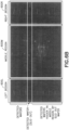
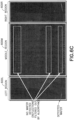
- Reflections detected in the middle region 600M but in the left region 600L and right region 600R for any given slot are mapped as being absent (e.g., an empty slot) (see Fig. 6C ).
- areas in the image corresponding to substrate holding slots in which a reflection in the middle region 600M exists but where there are no corresponding reflections in both the left region 600L and the right region 600R are mapped as being empty slots (i.e., substrate is absent).
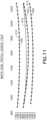
- Fig. 13 illustrates the corrected true profile 500TC of the slot 13 substrate, which exhibits a warp/bow. Further, it is noted that the spatial correction can be applied prior to or after the processing the image by slicing of the image into the vertical image slices 410-416.
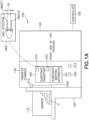
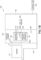
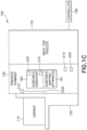
- the transport arm 180TA includes an end effector 180E movably mounted to the transport arm 180TA for loading substrates from the substrate carrier 110 through the opening 888 to the substrate processing apparatus 100, 150, 165 (and vice versa).
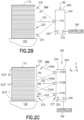
- each respective camera 210A, 210B, 210C is positioned with a field of view FOVA, FOVB, FOVC disposed to view, through the opening 888 with the common support 244 positioned by the transport arm 180TA at a common position CP, a different separate part of the substrate carrier 110 with wafer slots for holding at least one of the more one substrates S, separate and different from parts of the substrate carrier 110 with different wafer slots for holding substrates S different than the at least one substrate S viewed by each other camera 210A, 210B, 210C with the common support 244 at the common position CP, and each substrate S held in the substrate carrier 110 is imaged by the camera array 277 with the common support 244 at the common position CP.
- the at least one illuminator 220 is provided ( Fig. 14 , Block 1415) and is connected to the common support 244. As described above, the at least one illuminator is configured so as to illuminate, through the opening 888 with the common support 244 in the common position CP, an outer edge 233 of each substrate S in the substrate carrier 110, which edge delineates upper and lower edge boundaries 233U, 233L of the outer edge 233 of the substrate S.
- the at least one illuminator 220 is disposed with respect to each respective camera 210A, 210B, 210C, and the image of the corresponding separate different part (see, e.g., regions RA, RB, RC in Fig. 2C and the region of interest in Fig.
- each respective camera 210A, 210B, 210C is disposed so that the outer edge 233 directs reflected edge illumination, from the at least one illuminator 220, at the respective camera 210A, 210B, 210C, and optically blanks, at the upper edge boundary 233U and the lower edge boundary 233L, background reflection light, in the image captured of the separate different part of the substrate carrier 110 by the respective camera 210A, 210B, 210C through the opening 888 with the common support 244 at the common position CP.
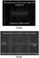
- the outer edge 233 of the substrate S is defined with the upper and lower edge boundaries 233U, 233L in relief in image contrast, formed by and between the edge reflection and the optically blanked background, registered by each camera 210A, 210B, 210C so as to effect edge detection of each substrate S in the substrate carrier 110 with the common support 244 at the common position CP.
- the controller 199 commands movement of the transfer arm 180TA so that the transfer arm 180TA is positioned relative to the opening 888 ( Fig. 14 , Block 1420) for imaging the substrates S within the carrier 110 through the opening 888.
- the substrates S are illuminated by the at least one illuminator 220 and images of the substrates S in the different separate regions (see, e.g., regions RA, RB, RC in Fig. 2C ) are captured through the opening 888 by camera array 277 ( Fig. 14 , Block 1425).
- the controller 199 is configured to perform one or more of determining a substrate map and determining substrate warp/bow. As described herein, mapping and determining warps/bows of substrates may be determined in any suitable order relative to one another such as where both are desired to be determined.
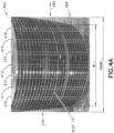
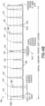
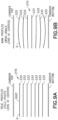
- the controller 199 determines the intensity profile 480 (see Figs. 4A and 4B ) in the manner described herein ( Fig. 14 , Block 1430) for each of the different separate regions (e.g., regions RA, RB, RC). From the intensity profile 480, the controller 199 determines the true edge profile 500T in the manner described herein ( Fig. 14 , Block 1440) and the so as to determine the substrate map 280 ( Fig. 14 , Block 1442) for each different separate region and the substrate carrier 110 as a whole. The substrate state (e.g., absent, present, double, cross, shift) is determined ( Fig.
- Any substrate warping/bowing of the substrates in the different separate regions RA, RB, RC is determined by the controller 199 in any suitable manner (such as with the image processing described herein) from the corrected true edge profiles 500TC of the substrates S ( Fig. 14 , Block 1467).
- the warping/bowing determination is employed by the controller 199 to adjust the distance TD (or spacing) (see FIG. 1A ) between end effector tines 180ET1, 180ET2 for picking the warped/bowed substrates S ( Fig. 14 , Block 1470).
- a semiconductor wafer mapping apparatus comprises: a frame forming a wafer load opening communicating with a load station for a substrate carrier disposed to hold more than one wafers vertically distributed in the substrate carrier for loading through the wafer load opening; a movable arm movably mounted to the frame so as to move relative to the wafer load opening and having at least one end effector movably mounted to the movable arm to load wafers from the substrate carrier through the wafer load opening; an image acquisition system including an array of cameras arranged on a common support and each camera is fixed with respect to the common support that is static with respect to each camera of the array of cameras, wherein each respective camera is positioned with a field of view disposed to view, through the wafer load opening with the common support positioned by the movable arm at a common position, a different separate part of the substrate carrier with wafer slots for holding at least one of the more one wafers, separate and different from parts of the substrate carrier with different wafer slots for holding wafer
- each different separate part viewed by the respective camera of the array of cameras has a different set of wafer slots, corresponding to the separate part and the respective camera, vertically distributed at predetermined reference heights viewed by the respective camera.
- the semiconductor wafer mapping apparatus further comprises a controller communicably coupled to the movable arm to move the movable arm relative to the frame and position the common support at the common position.
- a semiconductor wafer mapping apparatus comprises: a frame forming a wafer load opening communicating with a load station for a substrate carrier disposed to hold more than one wafers vertically distributed in the substrate carrier for loading through the wafer load opening; a movable arm movably mounted to the frame so as to move relative to the wafer load opening and having at least one end effector movably mounted to the movable arm to load wafers from the substrate carrier through the wafer load opening; an image acquisition system including an array of cameras arranged on a common support and each camera is fixed with respect to the common support that is static with respect to each camera of the array of cameras, wherein each respective camera is positioned with a field of view disposed to view, through the wafer load opening with the common support positioned by the movable arm at a common position, a corresponding different separate part of the substrate carrier each with at least one corresponding wafer slot different from at least one other wafer slot in each other corresponding different separate part of the substrate carrier, each
- each of the corresponding different separate part is imaged by but one respective camera of the array.
- each of at least one wafer held in the corresponding wafer slot of the corresponding different separate part is imaged by but one of the respective camera of the array of cameras.
- the semiconductor wafer mapping apparatus further comprises a controller communicably coupled to the array of cameras and programmed with each respective camera calibration, that has a baseline image for the respective camera, different from the baseline image of each other respective camera, the baseline image defining predetermined baseline characteristics for each of at least one wafer in each of the at least one corresponding slot of the corresponding separate different part imaged by the respective camera.
- the illumination source is dispose relative to the respective camera so that reflected light from planar surfaces of the wafer and each other wafer slotted in the substrate carrier are optically blanked in each image by the respective camera of the different separate part of the substrate carrier.
Landscapes
- Engineering & Computer Science (AREA)
- Computer Vision & Pattern Recognition (AREA)
- Physics & Mathematics (AREA)
- General Physics & Mathematics (AREA)
- Theoretical Computer Science (AREA)
- Container, Conveyance, Adherence, Positioning, Of Wafer (AREA)
Priority Applications (1)
| Application Number | Priority Date | Filing Date | Title |
|---|---|---|---|
| EP25179852.6A EP4589645A3 (en) | 2020-06-30 | 2021-06-30 | Substrate mapping apparatus and method therefor |
Applications Claiming Priority (3)
| Application Number | Priority Date | Filing Date | Title |
|---|---|---|---|
| US202063046555P | 2020-06-30 | 2020-06-30 | |
| US17/362,599 US12002696B2 (en) | 2020-06-30 | 2021-06-29 | Substrate mapping apparatus and method therefor |
| PCT/US2021/039966 WO2022006319A1 (en) | 2020-06-30 | 2021-06-30 | Substrate mapping apparatus and method therefor |
Related Child Applications (1)
| Application Number | Title | Priority Date | Filing Date |
|---|---|---|---|
| EP25179852.6A Division EP4589645A3 (en) | 2020-06-30 | 2021-06-30 | Substrate mapping apparatus and method therefor |
Publications (4)
| Publication Number | Publication Date |
|---|---|
| EP4171843A1 EP4171843A1 (en) | 2023-05-03 |
| EP4171843A4 EP4171843A4 (en) | 2024-01-17 |
| EP4171843B1 true EP4171843B1 (en) | 2025-06-25 |
| EP4171843C0 EP4171843C0 (en) | 2025-06-25 |
Family
ID=79031420
Family Applications (2)
| Application Number | Title | Priority Date | Filing Date |
|---|---|---|---|
| EP21834134.5A Active EP4171843B1 (en) | 2020-06-30 | 2021-06-30 | Substrate mapping apparatus and method therefor |
| EP25179852.6A Pending EP4589645A3 (en) | 2020-06-30 | 2021-06-30 | Substrate mapping apparatus and method therefor |
Family Applications After (1)
| Application Number | Title | Priority Date | Filing Date |
|---|---|---|---|
| EP25179852.6A Pending EP4589645A3 (en) | 2020-06-30 | 2021-06-30 | Substrate mapping apparatus and method therefor |
Country Status (6)
| Country | Link |
|---|---|
| US (3) | US12002696B2 (cg-RX-API-DMAC10.html) |
| EP (2) | EP4171843B1 (cg-RX-API-DMAC10.html) |
| JP (1) | JP7681628B2 (cg-RX-API-DMAC10.html) |
| CN (3) | CN120656970A (cg-RX-API-DMAC10.html) |
| TW (1) | TW202205494A (cg-RX-API-DMAC10.html) |
| WO (1) | WO2022006319A1 (cg-RX-API-DMAC10.html) |
Families Citing this family (17)
| Publication number | Priority date | Publication date | Assignee | Title |
|---|---|---|---|---|
| US11469123B2 (en) * | 2019-08-19 | 2022-10-11 | Applied Materials, Inc. | Mapping of a replacement parts storage container |
| JP7849187B2 (ja) * | 2022-02-24 | 2026-04-21 | 株式会社ディスコ | 搬送装置 |
| TWI831162B (zh) * | 2022-03-24 | 2024-02-01 | 上銀科技股份有限公司 | 裝載埠及其映射裝置 |
| JP7682831B2 (ja) * | 2022-04-27 | 2025-05-26 | 川崎重工業株式会社 | 半導体製造装置システム |
| KR102926940B1 (ko) * | 2022-05-27 | 2026-02-12 | (주)테크윙 | 핸들러 |
| WO2024010707A1 (en) * | 2022-07-08 | 2024-01-11 | Lam Research Corporation | Mobile sensor devices for semiconductor fabrication equipment |
| US12136225B2 (en) | 2022-09-09 | 2024-11-05 | Applied Materials, Inc. | Clog detection via image analytics |
| US12394647B2 (en) * | 2022-09-23 | 2025-08-19 | Taiwan Semiconductor Manufacturing Company, Ltd. | Wafer shift detection |
| US12707922B2 (en) * | 2022-11-21 | 2026-08-11 | Applied Materials, Inc. | Determining a substrate location threshold based on optical properties |
| JP2024080228A (ja) * | 2022-12-02 | 2024-06-13 | 株式会社安川電機 | 基板搬送装置および基板搬送方法 |
| CN122443811A (zh) * | 2023-03-28 | 2026-07-24 | Jcet星科金朋韩国有限公司 | 具有改进的翘曲控制的承载半导体封装条的载体组件 |
| JP2025047267A (ja) * | 2023-09-21 | 2025-04-03 | 株式会社Screenホールディングス | 基板搬送装置及びそれを備えた基板処理装置 |
| CN117438356B (zh) * | 2023-12-21 | 2024-04-19 | 浙江果纳半导体技术有限公司 | 一种自适应晶圆传输方法、可存储介质和晶圆传输设备 |
| US12677630B2 (en) | 2024-06-03 | 2026-07-07 | Applied Materials, Inc. | Identifying and weighing carriers in a substrate processing system |
| US20260026294A1 (en) * | 2024-07-19 | 2026-01-22 | Kla Corporation | Systems and methods for wafer overview image scan and pre-alignment of film frame carrier |
| WO2026112488A1 (en) * | 2024-11-22 | 2026-05-28 | Brooks Automation Us, Llc | Substrate processing apparatus and method |
| US20260148411A1 (en) * | 2024-11-28 | 2026-05-28 | Kla Corporation | Methods And Systems Of Film Frame Pre-Alignment For Semiconductor Measurement Equipment |
Family Cites Families (33)
| Publication number | Priority date | Publication date | Assignee | Title |
|---|---|---|---|---|
| JP4253365B2 (ja) * | 1997-10-17 | 2009-04-08 | オリンパス株式会社 | ウェハ搬送装置 |
| JP3380147B2 (ja) * | 1997-11-13 | 2003-02-24 | 大日本スクリーン製造株式会社 | 基板処理装置 |
| US6013920A (en) * | 1997-11-28 | 2000-01-11 | Fortrend Engineering Coirporation | Wafer-mapping load post interface having an effector position sensing device |
| DE19814046C1 (de) * | 1998-03-30 | 1999-11-18 | Jenoptik Jena Gmbh | Anordnung zur Detektion von scheibenförmigen Objekten in einer Kassette |
| JPH11354609A (ja) * | 1998-06-11 | 1999-12-24 | Mecs Corp | 薄型基板収容カセットの蓋開閉装置 |
| US6188323B1 (en) * | 1998-10-15 | 2001-02-13 | Asyst Technologies, Inc. | Wafer mapping system |
| US6636626B1 (en) | 1999-11-30 | 2003-10-21 | Wafermasters, Inc. | Wafer mapping apparatus and method |
| JP3699348B2 (ja) * | 2000-11-30 | 2005-09-28 | 平田機工株式会社 | 駆動部隔離foupオープナ |
| JP2002224982A (ja) * | 2000-12-01 | 2002-08-13 | Yaskawa Electric Corp | 薄型基板搬送用ロボットおよび薄型基板検出方法 |
| US6452503B1 (en) | 2001-03-15 | 2002-09-17 | Pri Automation, Inc. | Semiconductor wafer imaging system |
| US6825486B1 (en) | 2001-07-13 | 2004-11-30 | Cyberoptics Corporation | System for mapping wafers using predictive dynamic lighting |
| US6900451B2 (en) * | 2001-11-08 | 2005-05-31 | Multimextrixs, Llc | Mapping sensor system for detecting positions of flat objects |
| JP4196335B2 (ja) * | 2003-06-10 | 2008-12-17 | 株式会社安川電機 | 薄型基板検出方法 |
| US7015492B2 (en) | 2003-08-15 | 2006-03-21 | Asm International N.V. | Method and apparatus for mapping of wafers located inside a closed wafer cassette |
| US9691651B2 (en) * | 2005-01-28 | 2017-06-27 | Brooks Automation, Inc. | Substrate handling system for aligning and orienting substrates during a transfer operation |
| US20050086024A1 (en) * | 2003-09-19 | 2005-04-21 | Cyberoptics Semiconductor Inc. | Semiconductor wafer location sensing via non contact methods |
| JP2005167208A (ja) | 2003-10-24 | 2005-06-23 | Ade Corp | ノッチ化/フラット化200mmウエーハエッジグリップエンドエフェクタ |
| US7891936B2 (en) * | 2005-03-30 | 2011-02-22 | Brooks Automation, Inc. | High speed substrate aligner apparatus |
| US9105673B2 (en) | 2007-05-09 | 2015-08-11 | Brooks Automation, Inc. | Side opening unified pod |
| JP5185756B2 (ja) * | 2008-10-01 | 2013-04-17 | 川崎重工業株式会社 | 基板検出装置および方法 |
| JP5881007B2 (ja) | 2009-11-17 | 2016-03-09 | シンフォニアテクノロジー株式会社 | ウエハ検出装置 |
| KR102139617B1 (ko) | 2012-12-27 | 2020-07-31 | 세메스 주식회사 | 기판 이송 장치 및 방법 |
| JP6415220B2 (ja) * | 2014-09-29 | 2018-10-31 | 株式会社Screenホールディングス | 基板処理装置および基板処理方法 |
| US10755960B2 (en) * | 2014-11-04 | 2020-08-25 | Brooks Automation, Inc. | Wafer aligner |
| JP6571475B2 (ja) * | 2015-09-30 | 2019-09-04 | 株式会社Screenホールディングス | 基板処理装置 |
| SG10201906641WA (en) * | 2015-10-01 | 2019-09-27 | Intevac Inc | Wafer plate and mask arrangement for substrate fabrication |
| US10515834B2 (en) * | 2015-10-12 | 2019-12-24 | Lam Research Corporation | Multi-station tool with wafer transfer microclimate systems |
| US10607879B2 (en) | 2016-09-08 | 2020-03-31 | Brooks Automation, Inc. | Substrate processing apparatus |
| US10784134B2 (en) | 2017-05-03 | 2020-09-22 | Applied Materials, Inc. | Image based substrate mapper |
| US10714364B2 (en) * | 2017-08-31 | 2020-07-14 | Taiwan Semiconductor Manufacturing Co., Ltd. | Apparatus and method for inspecting wafer carriers |
| KR101843476B1 (ko) * | 2017-10-11 | 2018-03-29 | 주식회사 싸이맥스 | 로드포트모듈 비전 맵핑장치 및 로드포트모듈 비전 맵핑방법 |
| JP7073697B2 (ja) * | 2017-12-07 | 2022-05-24 | Tdk株式会社 | ロードポート |
| JP6804069B2 (ja) * | 2018-08-03 | 2020-12-23 | 株式会社Kokusai Electric | 基板処理システム、基板処理装置及び半導体装置の製造方法 |
-
2021
- 2021-06-29 US US17/362,599 patent/US12002696B2/en active Active
- 2021-06-30 JP JP2022581488A patent/JP7681628B2/ja active Active
- 2021-06-30 TW TW110124052A patent/TW202205494A/zh unknown
- 2021-06-30 EP EP21834134.5A patent/EP4171843B1/en active Active
- 2021-06-30 CN CN202510797176.2A patent/CN120656970A/zh active Pending
- 2021-06-30 CN CN202511151198.8A patent/CN121035002A/zh active Pending
- 2021-06-30 EP EP25179852.6A patent/EP4589645A3/en active Pending
- 2021-06-30 CN CN202180053513.7A patent/CN116056810B/zh active Active
- 2021-06-30 WO PCT/US2021/039966 patent/WO2022006319A1/en not_active Ceased
-
2024
- 2024-05-06 US US18/655,873 patent/US12564003B2/en active Active
-
2026
- 2026-02-24 US US19/548,520 patent/US20260190924A1/en active Pending
Also Published As
| Publication number | Publication date |
|---|---|
| CN116056810A (zh) | 2023-05-02 |
| TW202205494A (zh) | 2022-02-01 |
| US12564003B2 (en) | 2026-02-24 |
| US20260190924A1 (en) | 2026-07-02 |
| CN120656970A (zh) | 2025-09-16 |
| EP4171843A1 (en) | 2023-05-03 |
| US20210407831A1 (en) | 2021-12-30 |
| JP2023532334A (ja) | 2023-07-27 |
| KR20230029972A (ko) | 2023-03-03 |
| CN121035002A (zh) | 2025-11-28 |
| CN116056810B (zh) | 2025-09-05 |
| EP4589645A2 (en) | 2025-07-23 |
| EP4589645A3 (en) | 2026-01-21 |
| WO2022006319A1 (en) | 2022-01-06 |
| JP7681628B2 (ja) | 2025-05-22 |
| US20240290642A1 (en) | 2024-08-29 |
| EP4171843A4 (en) | 2024-01-17 |
| EP4171843C0 (en) | 2025-06-25 |
| US12002696B2 (en) | 2024-06-04 |
Similar Documents
| Publication | Publication Date | Title |
|---|---|---|
| US12564003B2 (en) | Substrate mapping apparatus and method therefor | |
| CN110709975B (zh) | 基于图像的基板映射器 | |
| JP5663207B2 (ja) | モジュラ光学検査システム | |
| JP2023532334A5 (cg-RX-API-DMAC10.html) | ||
| US20220336247A1 (en) | Method and apparatus for substrate alignment | |
| TWI428589B (zh) | 視覺檢測設備與方法 | |
| US20230187244A1 (en) | Method for inspecting a container and inspection system | |
| US20160133502A1 (en) | Wafer transfer robot, method of controlling the same, and method of manufacturing a semiconductor device using the same | |
| US20120300039A1 (en) | Apparatus and method for three dimensional inspection of wafer saw marks | |
| US20250349587A1 (en) | Workpiece handling system, method of calibrating workpiece handling system and method of manufacturing semiconductor package | |
| KR20210143118A (ko) | 표면 변형들의 이미지 기반 계측 | |
| US8379082B2 (en) | System, methods and apparatus for substrate carrier content verification using a material handling system | |
| TW202516665A (zh) | 基板搬送裝置及具備其之基板處理裝置 | |
| US20250290745A1 (en) | Apparatus and method for determining the surface profile of a semiconductor substrate using a laser scanning technique | |
| US20260015173A1 (en) | Mapping system | |
| JP2025042538A (ja) | 基板搬送ロボットシステム、および、基板検出方法 | |
| US20260067552A1 (en) | Apparatus for inspecting appearance of battery prismatic can | |
| KR20230021892A (ko) | 기판 검사 장치 및 기판 검사 방법 |
Legal Events
| Date | Code | Title | Description |
|---|---|---|---|
| STAA | Information on the status of an ep patent application or granted ep patent |
Free format text: STATUS: THE INTERNATIONAL PUBLICATION HAS BEEN MADE |
|
| PUAI | Public reference made under article 153(3) epc to a published international application that has entered the european phase |
Free format text: ORIGINAL CODE: 0009012 |
|
| STAA | Information on the status of an ep patent application or granted ep patent |
Free format text: STATUS: REQUEST FOR EXAMINATION WAS MADE |
|
| 17P | Request for examination filed |
Effective date: 20221223 |
|
| AK | Designated contracting states |
Kind code of ref document: A1 Designated state(s): AL AT BE BG CH CY CZ DE DK EE ES FI FR GB GR HR HU IE IS IT LI LT LU LV MC MK MT NL NO PL PT RO RS SE SI SK SM TR |
|
| DAV | Request for validation of the european patent (deleted) | ||
| DAX | Request for extension of the european patent (deleted) | ||
| A4 | Supplementary search report drawn up and despatched |
Effective date: 20231218 |
|
| RIC1 | Information provided on ipc code assigned before grant |
Ipc: H01L 21/68 20060101ALI20231212BHEP Ipc: H01L 21/677 20060101ALI20231212BHEP Ipc: H01L 21/67 20060101ALI20231212BHEP Ipc: G06T 7/73 20170101ALI20231212BHEP Ipc: G06T 7/13 20170101ALI20231212BHEP Ipc: B44C 1/22 20060101ALI20231212BHEP Ipc: B08B 3/08 20060101ALI20231212BHEP Ipc: B08B 3/00 20060101AFI20231212BHEP |
|
| GRAP | Despatch of communication of intention to grant a patent |
Free format text: ORIGINAL CODE: EPIDOSNIGR1 |
|
| STAA | Information on the status of an ep patent application or granted ep patent |
Free format text: STATUS: GRANT OF PATENT IS INTENDED |
|
| INTG | Intention to grant announced |
Effective date: 20250130 |
|
| GRAS | Grant fee paid |
Free format text: ORIGINAL CODE: EPIDOSNIGR3 |
|
| GRAA | (expected) grant |
Free format text: ORIGINAL CODE: 0009210 |
|
| STAA | Information on the status of an ep patent application or granted ep patent |
Free format text: STATUS: THE PATENT HAS BEEN GRANTED |
|
| AK | Designated contracting states |
Kind code of ref document: B1 Designated state(s): AL AT BE BG CH CY CZ DE DK EE ES FI FR GB GR HR HU IE IS IT LI LT LU LV MC MK MT NL NO PL PT RO RS SE SI SK SM TR |
|
| REG | Reference to a national code |
Ref country code: GB Ref legal event code: FG4D |
|
| REG | Reference to a national code |
Ref country code: CH Ref legal event code: EP |
|
| REG | Reference to a national code |
Ref country code: DE Ref legal event code: R096 Ref document number: 602021033027 Country of ref document: DE |
|
| REG | Reference to a national code |
Ref country code: CH Ref legal event code: EP |
|
| REG | Reference to a national code |
Ref country code: IE Ref legal event code: FG4D |
|
| U01 | Request for unitary effect filed |
Effective date: 20250725 |
|
| U07 | Unitary effect registered |
Designated state(s): AT BE BG DE DK EE FI FR IT LT LU LV MT NL PT RO SE SI Effective date: 20250730 |
|
| PG25 | Lapsed in a contracting state [announced via postgrant information from national office to epo] |
Ref country code: NO Free format text: LAPSE BECAUSE OF FAILURE TO SUBMIT A TRANSLATION OF THE DESCRIPTION OR TO PAY THE FEE WITHIN THE PRESCRIBED TIME-LIMIT Effective date: 20250925 Ref country code: GR Free format text: LAPSE BECAUSE OF FAILURE TO SUBMIT A TRANSLATION OF THE DESCRIPTION OR TO PAY THE FEE WITHIN THE PRESCRIBED TIME-LIMIT Effective date: 20250926 |
|
| PG25 | Lapsed in a contracting state [announced via postgrant information from national office to epo] |
Ref country code: HR Free format text: LAPSE BECAUSE OF FAILURE TO SUBMIT A TRANSLATION OF THE DESCRIPTION OR TO PAY THE FEE WITHIN THE PRESCRIBED TIME-LIMIT Effective date: 20250625 |
|
| PG25 | Lapsed in a contracting state [announced via postgrant information from national office to epo] |
Ref country code: RS Free format text: LAPSE BECAUSE OF FAILURE TO SUBMIT A TRANSLATION OF THE DESCRIPTION OR TO PAY THE FEE WITHIN THE PRESCRIBED TIME-LIMIT Effective date: 20250925 |
|
| U20 | Renewal fee for the european patent with unitary effect paid |
Year of fee payment: 5 Effective date: 20251020 |
|
| PG25 | Lapsed in a contracting state [announced via postgrant information from national office to epo] |
Ref country code: IS Free format text: LAPSE BECAUSE OF FAILURE TO SUBMIT A TRANSLATION OF THE DESCRIPTION OR TO PAY THE FEE WITHIN THE PRESCRIBED TIME-LIMIT Effective date: 20251025 |
|
| PG25 | Lapsed in a contracting state [announced via postgrant information from national office to epo] |
Ref country code: SM Free format text: LAPSE BECAUSE OF FAILURE TO SUBMIT A TRANSLATION OF THE DESCRIPTION OR TO PAY THE FEE WITHIN THE PRESCRIBED TIME-LIMIT Effective date: 20250625 |
|
| PG25 | Lapsed in a contracting state [announced via postgrant information from national office to epo] |
Ref country code: CZ Free format text: LAPSE BECAUSE OF FAILURE TO SUBMIT A TRANSLATION OF THE DESCRIPTION OR TO PAY THE FEE WITHIN THE PRESCRIBED TIME-LIMIT Effective date: 20250625 |
|
| PG25 | Lapsed in a contracting state [announced via postgrant information from national office to epo] |
Ref country code: PL Free format text: LAPSE BECAUSE OF FAILURE TO SUBMIT A TRANSLATION OF THE DESCRIPTION OR TO PAY THE FEE WITHIN THE PRESCRIBED TIME-LIMIT Effective date: 20250625 |
|
| PG25 | Lapsed in a contracting state [announced via postgrant information from national office to epo] |
Ref country code: SK Free format text: LAPSE BECAUSE OF FAILURE TO SUBMIT A TRANSLATION OF THE DESCRIPTION OR TO PAY THE FEE WITHIN THE PRESCRIBED TIME-LIMIT Effective date: 20250625 |
|
| REG | Reference to a national code |
Ref country code: CH Ref legal event code: H13 Free format text: ST27 STATUS EVENT CODE: U-0-0-H10-H13 (AS PROVIDED BY THE NATIONAL OFFICE) Effective date: 20260127 |
|
| PG25 | Lapsed in a contracting state [announced via postgrant information from national office to epo] |
Ref country code: ES Free format text: LAPSE BECAUSE OF FAILURE TO SUBMIT A TRANSLATION OF THE DESCRIPTION OR TO PAY THE FEE WITHIN THE PRESCRIBED TIME-LIMIT Effective date: 20250625 |
|
| PG25 | Lapsed in a contracting state [announced via postgrant information from national office to epo] |
Ref country code: MC Free format text: LAPSE BECAUSE OF FAILURE TO SUBMIT A TRANSLATION OF THE DESCRIPTION OR TO PAY THE FEE WITHIN THE PRESCRIBED TIME-LIMIT Effective date: 20250625 |
|
| PG25 | Lapsed in a contracting state [announced via postgrant information from national office to epo] |
Ref country code: IE Free format text: LAPSE BECAUSE OF NON-PAYMENT OF DUE FEES Effective date: 20250630 |
|
| PG25 | Lapsed in a contracting state [announced via postgrant information from national office to epo] |
Ref country code: CH Free format text: LAPSE BECAUSE OF NON-PAYMENT OF DUE FEES Effective date: 20250630 |
|
| PLBE | No opposition filed within time limit |
Free format text: ORIGINAL CODE: 0009261 |
|
| STAA | Information on the status of an ep patent application or granted ep patent |
Free format text: STATUS: NO OPPOSITION FILED WITHIN TIME LIMIT |
|
| REG | Reference to a national code |
Ref country code: CH Ref legal event code: L10 Free format text: ST27 STATUS EVENT CODE: U-0-0-L10-L00 (AS PROVIDED BY THE NATIONAL OFFICE) Effective date: 20260507 |
|
| GBPC | Gb: european patent ceased through non-payment of renewal fee |
Effective date: 20250925 |
|
| 26N | No opposition filed |
Effective date: 20260326 |
|
| U20 | Renewal fee for the european patent with unitary effect paid |
Year of fee payment: 6 Effective date: 20260520 |
|
| PG25 | Lapsed in a contracting state [announced via postgrant information from national office to epo] |
Ref country code: GB Free format text: LAPSE BECAUSE OF NON-PAYMENT OF DUE FEES Effective date: 20250925 |
|
| PG25 | Lapsed in a contracting state [announced via postgrant information from national office to epo] |
Ref country code: CY Free format text: LAPSE BECAUSE OF FAILURE TO SUBMIT A TRANSLATION OF THE DESCRIPTION OR TO PAY THE FEE WITHIN THE PRESCRIBED TIME-LIMIT Effective date: 20250625 |