EP4170435A1 - Verfahren zur herstellung eines verkleidungsteils, insbesondere eines verkleidungsteils für uhren - Google Patents
Verfahren zur herstellung eines verkleidungsteils, insbesondere eines verkleidungsteils für uhren Download PDFInfo
- Publication number
- EP4170435A1 EP4170435A1 EP21204426.7A EP21204426A EP4170435A1 EP 4170435 A1 EP4170435 A1 EP 4170435A1 EP 21204426 A EP21204426 A EP 21204426A EP 4170435 A1 EP4170435 A1 EP 4170435A1
- Authority
- EP
- European Patent Office
- Prior art keywords
- coating
- substrate
- orifices
- structuring
- deposition
- Prior art date
- Legal status (The legal status is an assumption and is not a legal conclusion. Google has not performed a legal analysis and makes no representation as to the accuracy of the status listed.)
- Withdrawn
Links
- 238000000034 method Methods 0.000 title claims abstract description 25
- 238000004519 manufacturing process Methods 0.000 title claims abstract description 8
- 239000011248 coating agent Substances 0.000 claims abstract description 41
- 238000000576 coating method Methods 0.000 claims abstract description 41
- 239000000758 substrate Substances 0.000 claims abstract description 37
- 238000000151 deposition Methods 0.000 claims abstract description 21
- 238000009826 distribution Methods 0.000 claims abstract description 16
- 230000005855 radiation Effects 0.000 claims abstract description 7
- 239000010410 layer Substances 0.000 claims description 23
- 230000008021 deposition Effects 0.000 claims description 16
- MCMNRKCIXSYSNV-UHFFFAOYSA-N Zirconium dioxide Chemical compound O=[Zr]=O MCMNRKCIXSYSNV-UHFFFAOYSA-N 0.000 claims description 12
- 239000002346 layers by function Substances 0.000 claims description 10
- 239000000463 material Substances 0.000 claims description 10
- VYZAMTAEIAYCRO-UHFFFAOYSA-N Chromium Chemical compound [Cr] VYZAMTAEIAYCRO-UHFFFAOYSA-N 0.000 claims description 6
- RTAQQCXQSZGOHL-UHFFFAOYSA-N Titanium Chemical compound [Ti] RTAQQCXQSZGOHL-UHFFFAOYSA-N 0.000 claims description 6
- 229910052804 chromium Inorganic materials 0.000 claims description 6
- 239000011651 chromium Substances 0.000 claims description 6
- 239000011241 protective layer Substances 0.000 claims description 6
- 239000010936 titanium Substances 0.000 claims description 6
- 229910052719 titanium Inorganic materials 0.000 claims description 6
- 239000011521 glass Substances 0.000 claims description 4
- 229910052594 sapphire Inorganic materials 0.000 claims description 4
- 239000010980 sapphire Substances 0.000 claims description 4
- 238000001771 vacuum deposition Methods 0.000 claims description 4
- PCHJSUWPFVWCPO-UHFFFAOYSA-N gold Chemical compound [Au] PCHJSUWPFVWCPO-UHFFFAOYSA-N 0.000 claims description 3
- 229910052737 gold Inorganic materials 0.000 claims description 3
- 239000010931 gold Substances 0.000 claims description 3
- 238000000206 photolithography Methods 0.000 claims description 3
- 229910052709 silver Inorganic materials 0.000 claims description 3
- 239000004332 silver Substances 0.000 claims description 3
- 235000015243 ice cream Nutrition 0.000 claims 1
- 239000013078 crystal Substances 0.000 description 4
- 239000003086 colorant Substances 0.000 description 3
- 238000005034 decoration Methods 0.000 description 3
- 229910052751 metal Inorganic materials 0.000 description 3
- 239000002184 metal Substances 0.000 description 3
- 239000000203 mixture Substances 0.000 description 3
- IJGRMHOSHXDMSA-UHFFFAOYSA-N Atomic nitrogen Chemical compound N#N IJGRMHOSHXDMSA-UHFFFAOYSA-N 0.000 description 2
- 230000005540 biological transmission Effects 0.000 description 2
- 238000003754 machining Methods 0.000 description 2
- 150000002739 metals Chemical class 0.000 description 2
- 230000003287 optical effect Effects 0.000 description 2
- 239000010970 precious metal Substances 0.000 description 2
- 239000002356 single layer Substances 0.000 description 2
- 238000002834 transmittance Methods 0.000 description 2
- 241001080024 Telles Species 0.000 description 1
- QVGXLLKOCUKJST-UHFFFAOYSA-N atomic oxygen Chemical compound [O] QVGXLLKOCUKJST-UHFFFAOYSA-N 0.000 description 1
- 238000005229 chemical vapour deposition Methods 0.000 description 1
- 230000007423 decrease Effects 0.000 description 1
- 238000005516 engineering process Methods 0.000 description 1
- 230000003116 impacting effect Effects 0.000 description 1
- 239000007769 metal material Substances 0.000 description 1
- 229910052757 nitrogen Inorganic materials 0.000 description 1
- 239000001301 oxygen Substances 0.000 description 1
- 229910052760 oxygen Inorganic materials 0.000 description 1
- 238000005240 physical vapour deposition Methods 0.000 description 1
- 239000000126 substance Substances 0.000 description 1
- 230000004304 visual acuity Effects 0.000 description 1
Images
Classifications
-
- G—PHYSICS
- G04—HOROLOGY
- G04B—MECHANICALLY-DRIVEN CLOCKS OR WATCHES; MECHANICAL PARTS OF CLOCKS OR WATCHES IN GENERAL; TIME PIECES USING THE POSITION OF THE SUN, MOON OR STARS
- G04B37/00—Cases
- G04B37/22—Materials or processes of manufacturing pocket watch or wrist watch cases
-
- A—HUMAN NECESSITIES
- A44—HABERDASHERY; JEWELLERY
- A44C—PERSONAL ADORNMENTS, e.g. JEWELLERY; COINS
- A44C11/00—Watch chains; Ornamental chains
-
- B—PERFORMING OPERATIONS; TRANSPORTING
- B44—DECORATIVE ARTS
- B44C—PRODUCING DECORATIVE EFFECTS; MOSAICS; TARSIA WORK; PAPERHANGING
- B44C1/00—Processes, not specifically provided for elsewhere, for producing decorative surface effects
- B44C1/22—Removing surface-material, e.g. by engraving, by etching
- B44C1/227—Removing surface-material, e.g. by engraving, by etching by etching
-
- B—PERFORMING OPERATIONS; TRANSPORTING
- B44—DECORATIVE ARTS
- B44C—PRODUCING DECORATIVE EFFECTS; MOSAICS; TARSIA WORK; PAPERHANGING
- B44C3/00—Processes, not specifically provided for elsewhere, for producing ornamental structures
- B44C3/005—Removing selectively parts of at least the upper layer of a multi-layer article
-
- B—PERFORMING OPERATIONS; TRANSPORTING
- B44—DECORATIVE ARTS
- B44C—PRODUCING DECORATIVE EFFECTS; MOSAICS; TARSIA WORK; PAPERHANGING
- B44C3/00—Processes, not specifically provided for elsewhere, for producing ornamental structures
- B44C3/02—Superimposing layers
-
- G—PHYSICS
- G03—PHOTOGRAPHY; CINEMATOGRAPHY; ANALOGOUS TECHNIQUES USING WAVES OTHER THAN OPTICAL WAVES; ELECTROGRAPHY; HOLOGRAPHY
- G03F—PHOTOMECHANICAL PRODUCTION OF TEXTURED OR PATTERNED SURFACES, e.g. FOR PRINTING, FOR PROCESSING OF SEMICONDUCTOR DEVICES; MATERIALS THEREFOR; ORIGINALS THEREFOR; APPARATUS SPECIALLY ADAPTED THEREFOR
- G03F7/00—Photomechanical, e.g. photolithographic, production of textured or patterned surfaces, e.g. printing surfaces; Materials therefor, e.g. comprising photoresists; Apparatus specially adapted therefor
- G03F7/20—Exposure; Apparatus therefor
- G03F7/2051—Exposure without an original mask, e.g. using a programmed deflection of a point source, by scanning, by drawing with a light beam, using an addressed light or corpuscular source
- G03F7/2053—Exposure without an original mask, e.g. using a programmed deflection of a point source, by scanning, by drawing with a light beam, using an addressed light or corpuscular source using a laser
-
- G—PHYSICS
- G04—HOROLOGY
- G04B—MECHANICALLY-DRIVEN CLOCKS OR WATCHES; MECHANICAL PARTS OF CLOCKS OR WATCHES IN GENERAL; TIME PIECES USING THE POSITION OF THE SUN, MOON OR STARS
- G04B19/00—Indicating the time by visual means
- G04B19/06—Dials
- G04B19/12—Selection of materials for dials or graduations markings
-
- G—PHYSICS
- G04—HOROLOGY
- G04B—MECHANICALLY-DRIVEN CLOCKS OR WATCHES; MECHANICAL PARTS OF CLOCKS OR WATCHES IN GENERAL; TIME PIECES USING THE POSITION OF THE SUN, MOON OR STARS
- G04B29/00—Frameworks
- G04B29/02—Plates; Bridges; Cocks
-
- G—PHYSICS
- G04—HOROLOGY
- G04B—MECHANICALLY-DRIVEN CLOCKS OR WATCHES; MECHANICAL PARTS OF CLOCKS OR WATCHES IN GENERAL; TIME PIECES USING THE POSITION OF THE SUN, MOON OR STARS
- G04B39/00—Watch crystals; Fastening or sealing of crystals; Clock glasses
-
- G—PHYSICS
- G04—HOROLOGY
- G04B—MECHANICALLY-DRIVEN CLOCKS OR WATCHES; MECHANICAL PARTS OF CLOCKS OR WATCHES IN GENERAL; TIME PIECES USING THE POSITION OF THE SUN, MOON OR STARS
- G04B45/00—Time pieces of which the indicating means or cases provoke special effects, e.g. aesthetic effects
- G04B45/0076—Decoration of the case and of parts thereof, e.g. as a method of manufacture thereof
-
- G—PHYSICS
- G04—HOROLOGY
- G04D—APPARATUS OR TOOLS SPECIALLY DESIGNED FOR MAKING OR MAINTAINING CLOCKS OR WATCHES
- G04D3/00—Watchmakers' or watch-repairers' machines or tools for working materials
- G04D3/0074—Watchmakers' or watch-repairers' machines or tools for working materials for treatment of the material, e.g. surface treatment
- G04D3/0092—Watchmakers' or watch-repairers' machines or tools for working materials for treatment of the material, e.g. surface treatment for components of the time-indicating mechanism, e.g. dials
Definitions
- the invention relates to the field of components for covering fashion items, and relates to a method of manufacturing a covering part intended in particular for a timepiece.
- the present invention can be applied to a piece of jewelry or to an article of eyewear.
- Such a covering part can be a dial, a dial counter, a bezel, a crystal, etc.
- the object of the present invention is to solve in particular this problem of misalignment of the structuring of layers of a coating of a substrate.
- the invention solves the aforementioned drawbacks by proposing a solution making it possible to obtain on a trim part a decoration which may have various colors, while guaranteeing compliance with the dimensional requirements of said decoration.
- the method since the method only has a single structuring step, the dimensional requirements for producing the decorative graphic representation are easier to comply with.
- the invention may also include one or more of the following characteristics, taken separately or in all technically possible combinations.
- the structuring step 300 is carried out so that the orifices form patterns respectively having distribution densities which are specific to them.
- the substrate is polished.
- the step of depositing 200 is made by vacuum deposition method.
- the deposition step 200 can be carried out in several vacuum deposition operations, if the coating is composed of several layers.
- the coating has a lower level of transparency than the level of transparency of the substrate.
- the structuring step 300 is carried out by photolithography or by direct structuring by laser.
- the deposition step 200 consists in depositing a single layer.
- the tie layer is made of chromium, titanium, zirconia, or oxynitrides of these materials
- the functional layer is made of gold or silver
- the protective layer is made in chromium, titanium or zirconia, or in oxynitride of these materials.
- the substrate is made of glass, sapphire or mother-of-pearl.
- orifices are made so as to have dimensions such that they are substantially invisible to the naked eye.
- orifices are made so that their cross section has a circular shape whose diameter is less than 50 micrometers.
- orifices are made so that their cross section has a polygonal shape, the dimensions of which are between 5 and 50 micrometers in width, and 5 and 500 micrometers in length.
- the present invention relates to a timepiece comprising a casing part made by implementing a method as described previously, in which the casing part forms a dial or a crystal.
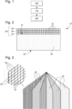
- FIG. 1 shows a flowchart representing the steps of a method of manufacturing a trim piece 10 comprising a decorative graphic representation according to the present invention.
- Such a graphic representation can be a logo, a decorative image, an inscription, etc.
- the trim piece 10 is shown in cross-sectional view on the figure 2 and in front view on the picture 3 .
- the covering part 10 can be a crystal, a dial, a dial counter, a bezel, etc. for a timepiece, in particular a watch.
- the covering part 10 comprises a coating 20 extending over all or part of the surface of one face of a transparent or partially transparent substrate 30, said face being intended to receive incident or transmitted light radiation.
- the coating 20 is deposited during a deposition step 200.
- partially transparent designates, in the present text, a capacity of an element to be translucent. This capacity is obtained by the nature of the material constituting the element and/or by the thickness of said element.
- the substrate 30 is made of sapphire, glass or mother-of-pearl, or any other material that may have a high or sufficient transparency for carrying out the present invention, and suitable mechanical characteristics.
- the substrate can be made of glass or sapphire if the covering part 10 forms a crystal, or the substrate can be made of mother-of-pearl if the trim part 10 forms a dial.
- the substrate 30 can be colored, either before the deposition step 200, or after the structuring step 300.
- the substrate 30 can advantageously be polished during a preliminary step 100 carried out before the step 200 of depositing the coating 20, in order to reduce the asperities and the roughness on its surface.
- this preliminary step 100 makes it possible to obtain a smooth and shiny state for the surfaces of the substrate 30.
- the substrate has a matte appearance.
- the coating 20 can be arranged on the surface of an external face 32 or of an internal face 31 of the substrate 30.
- the internal face 31 of the substrate 30 is intended to be arranged facing a watch movement and the external face 32 is intended to be arranged facing an external environment; in particular with regard to a user.
- the substrate 30 has a structural function insofar as its thickness is chosen so that it has sufficient rigidity to hold the trim piece 10 in position and resist the mechanical stresses. .
- the coating 20 can be partially transparent, that is to say translucent, or opaque, it being understood that it preferentially absorbs more light than does the substrate. In other words, the coating 20 has less transparency than the substrate.
- Transparency can in particular be defined by a light transmission test of light radiation of a given wavelength through a plate of material. Such a test is within the reach of those skilled in the art. Transparency is expressed as a percentage of transmission.
- coating 20 can be configured to have a percent transmittance of less than 60% and substrate 30 can be configured to have a percent transmittance of greater than 60%.
- the desired level of transparency is obtained by the choice of the material and/or the thickness of the element considered, in particular respectively of the coating 20 and of the substrate 30.
- the coating 20 can be made partially or totally of metallic material.
- the deposition step 200 can advantageously be carried out by a vacuum deposition method, for example physical vapor deposition or by a chemical vapor deposition method. This deposition step 200 can be carried out in one operation, if the coating is composed of a single layer, or in several operations if the coating 20 is composed of several layers, as described below.
- the coating 20 comprises a plurality of through holes 21 made during a structuring step 300 according to a distribution density such that the coating 20 forms the decorative graphic representation.
- the orifices 21 have for example dimensions such that they can be substantially invisible to the naked eye, the resolving power of the human eye being of the order of 70 micrometers at a distance of 25 centimeters.
- the dimensions here refer to the diameter of the orifices 21 if they have a cross-section of circular shape, or to the length and to the width if they have a cross-section of polygonal shape.
- the orifices have straight sections of polygonal shape.
- the dimensions of the orifices can vary between a few micrometers and a few tens of micrometers in width, for example between 5 and 50 micrometers, and vary between a few micrometers and a few hundred micrometers in length, for example between 5 and 500 micrometers.
- the orifices can also extend in elongated shapes over more than 500 micrometers in length and have a width of a few micrometers or tens of micrometers.
- the orifices 21 may have a cross-section of circular shape, the diameter of which is less than 50 micrometers.
- the light radiation can circulate through the orifices 21 and the substrate 30, within which an optical phenomenon of diffraction is generated.
- the structuring step 300 is carried out by laser machining, by chemical machining, by photolithography, by direct structuring by laser, or by any other suitable material removal method.
- the structuring step 300 is carried out so that the distribution of the orifices 21 formed, as well as their respective dimensions, are chosen so that the coating 20 materializes the decorative graphic representation.
- the distribution density of the orifices 21 is defined according to the graphic representation which it is desired to reproduce.
- the coating 20 may comprise several zones each comprising a different density of distribution of orifices 21 of the others, each zone forming a pattern 22, as shown in the picture 3 .
- the deposition step 200 can be carried out so as to form the coating 20 on a part of the surface of the substrate 30 defining the surface of the patterns 22 and the structuring step 300 can be carried out so as to locally generate distribution densities of the different orifices 21 on the surface of the trim part 10.
- the orifices 21 of one or more patterns 22 may have shapes identical to that of the orifices 21 of the other patterns 22, or alternatively, the orifices 21 of a pattern 22 may have shapes different from those of the orifices 21 one or more patterns 22.
- the orifices 21 may have cross sections of identical or different shape, depending on the graphic representation to be materialized.
- the orifices 21 can be distributed homogeneously or heterogeneously within the patterns 22.
- the orifices 21 can be arranged so that their density distribution changes gradually from one end to the other of the pattern 22, so as to create the desired graphic representation.
- the structuring step 300 is carried out only in the coating 20, that is to say without impacting the substrate 30.
- the substrate 30 being transparent or partially transparent and the coating 20 partially transparent or opaque, the structuring of the coating 20 generates an optical effect giving the trim part 10 a " matte” i.e. decreases the reflection and overall shine of the layer in these areas.
- the present invention makes it possible to represent variations of a color of the covering piece 10, for example shades, according to the distribution density of the orifices 21. More particularly, the more the distribution of the orifices 21 is dense, the more the color of the substrate 30 is visible, contrary to that of the coating 20, and the less the distribution of the orifices 21 is dense, the more the color of the coating 20 is visible, contrary to that of the substrate 30.
- the coating 20 may comprise three layers, among which a bonding layer 23 deposited directly on the substrate 30, a functional layer 24 deposited on the bonding layer 23, and a protective layer 25 deposited on the functional layer 24.
- bonding layer 23 can be made of chromium, titanium or zirconia, or a mixture of metals or their oxynitrides;
- the functional layer 24 can be made of gold, silver, or another precious metal;
- the protective layer 25 can be made of chromium, titanium, zirconia or a mixture of metals or oxynitrides of these materials.
- the bond 23 and protection 25 layers can be made of metal oxynitrides, of the MOxNy type, the oxygen and nitrogen composition being variable and possibly zero.
- the adhesion 23, functional 24 and protection 25 layers of the coating 20 are successively deposited on the substrate 30 during the deposition step 200, then the structuring step 300 is carried out.
- This embodiment of the coating 20 comprising a plurality of layers is preferred when the coating 20 is made from precious metals.
- the coating 20 could alternatively consist solely of the functional layer 24.
Landscapes
- Physics & Mathematics (AREA)
- General Physics & Mathematics (AREA)
- Engineering & Computer Science (AREA)
- Chemical & Material Sciences (AREA)
- Manufacturing & Machinery (AREA)
- Mechanical Engineering (AREA)
- Materials Engineering (AREA)
- Chemical Kinetics & Catalysis (AREA)
- Metallurgy (AREA)
- Organic Chemistry (AREA)
- Optics & Photonics (AREA)
- Laminated Bodies (AREA)
- General Chemical & Material Sciences (AREA)
- Electrochemistry (AREA)
- Physical Vapour Deposition (AREA)
- Surface Treatment Of Glass (AREA)
- Plasma & Fusion (AREA)
Priority Applications (6)
| Application Number | Priority Date | Filing Date | Title |
|---|---|---|---|
| EP21204426.7A EP4170435A1 (de) | 2021-10-25 | 2021-10-25 | Verfahren zur herstellung eines verkleidungsteils, insbesondere eines verkleidungsteils für uhren |
| EP21207803.4A EP4170434A1 (de) | 2021-10-25 | 2021-11-11 | Verfahren zur dekoration eines substrats |
| US17/938,140 US20230126038A1 (en) | 2021-10-25 | 2022-10-05 | Method for decorating a substrate |
| KR1020220130728A KR20230059143A (ko) | 2021-10-25 | 2022-10-12 | 기판의 장식 방법 |
| JP2022165234A JP7446380B2 (ja) | 2021-10-25 | 2022-10-14 | 基材を装飾する方法 |
| CN202211293143.7A CN116027652A (zh) | 2021-10-25 | 2022-10-21 | 装饰基底的方法 |
Applications Claiming Priority (1)
| Application Number | Priority Date | Filing Date | Title |
|---|---|---|---|
| EP21204426.7A EP4170435A1 (de) | 2021-10-25 | 2021-10-25 | Verfahren zur herstellung eines verkleidungsteils, insbesondere eines verkleidungsteils für uhren |
Publications (1)
| Publication Number | Publication Date |
|---|---|
| EP4170435A1 true EP4170435A1 (de) | 2023-04-26 |
Family
ID=78621644
Family Applications (2)
| Application Number | Title | Priority Date | Filing Date |
|---|---|---|---|
| EP21204426.7A Withdrawn EP4170435A1 (de) | 2021-10-25 | 2021-10-25 | Verfahren zur herstellung eines verkleidungsteils, insbesondere eines verkleidungsteils für uhren |
| EP21207803.4A Pending EP4170434A1 (de) | 2021-10-25 | 2021-11-11 | Verfahren zur dekoration eines substrats |
Family Applications After (1)
| Application Number | Title | Priority Date | Filing Date |
|---|---|---|---|
| EP21207803.4A Pending EP4170434A1 (de) | 2021-10-25 | 2021-11-11 | Verfahren zur dekoration eines substrats |
Country Status (5)
| Country | Link |
|---|---|
| US (1) | US20230126038A1 (de) |
| EP (2) | EP4170435A1 (de) |
| JP (1) | JP7446380B2 (de) |
| KR (1) | KR20230059143A (de) |
| CN (1) | CN116027652A (de) |
Citations (5)
| Publication number | Priority date | Publication date | Assignee | Title |
|---|---|---|---|---|
| EP1331529A1 (de) * | 2000-11-01 | 2003-07-30 | Kawaguchiko Seimitsu Company Limited | Zeitgeber-wähler und herstellungsverfahren dafür |
| US20160218234A1 (en) * | 2015-01-23 | 2016-07-28 | Sistine Solar, Inc. | Graphic layers and related methods for incorporation of graphic layers into solar modules |
| EP3339980A1 (de) * | 2016-12-22 | 2018-06-27 | The Swatch Group Research and Development Ltd | Verfahren zur erzeugung eines dekormotivs auf einer uhr, und entsprechende uhr |
| CH713871A1 (fr) * | 2017-07-27 | 2019-01-31 | Richemont Int Sa | Composant horloger comprenant des éléments graphiques de divers aspects et procédé de fabrication d'un tel composant. |
| US20210011434A1 (en) * | 2019-07-08 | 2021-01-14 | Seiko Epson Corporation | Watch Component and Watch |
Family Cites Families (4)
| Publication number | Priority date | Publication date | Assignee | Title |
|---|---|---|---|---|
| JPH04160154A (ja) * | 1990-10-24 | 1992-06-03 | Seiko Epson Corp | 装飾部材の製造方法 |
| EP3035128B1 (de) * | 2014-12-17 | 2020-09-16 | Nivarox-FAR S.A. | Herstellungsverfahren eines Dekorelements einer Uhr oder eines Schmuckstücks |
| EP3035129B1 (de) * | 2014-12-19 | 2020-11-04 | The Swatch Group Research and Development Ltd | Herstellungsverfahren eines Dekorelements für eine Uhr oder ein Schmuckstück |
| CH713250B1 (fr) * | 2016-12-16 | 2021-01-29 | Rubattel Et Weyermann S A | Procédé de fabrication d'un élément d'habillage, notamment d'un cadran, d'horlogerie ou de bijouterie, en matériau non conducteur et comportant des décors gravés métallisés et/ou colorés. |
-
2021
- 2021-10-25 EP EP21204426.7A patent/EP4170435A1/de not_active Withdrawn
- 2021-11-11 EP EP21207803.4A patent/EP4170434A1/de active Pending
-
2022
- 2022-10-05 US US17/938,140 patent/US20230126038A1/en active Pending
- 2022-10-12 KR KR1020220130728A patent/KR20230059143A/ko not_active Application Discontinuation
- 2022-10-14 JP JP2022165234A patent/JP7446380B2/ja active Active
- 2022-10-21 CN CN202211293143.7A patent/CN116027652A/zh active Pending
Patent Citations (5)
| Publication number | Priority date | Publication date | Assignee | Title |
|---|---|---|---|---|
| EP1331529A1 (de) * | 2000-11-01 | 2003-07-30 | Kawaguchiko Seimitsu Company Limited | Zeitgeber-wähler und herstellungsverfahren dafür |
| US20160218234A1 (en) * | 2015-01-23 | 2016-07-28 | Sistine Solar, Inc. | Graphic layers and related methods for incorporation of graphic layers into solar modules |
| EP3339980A1 (de) * | 2016-12-22 | 2018-06-27 | The Swatch Group Research and Development Ltd | Verfahren zur erzeugung eines dekormotivs auf einer uhr, und entsprechende uhr |
| CH713871A1 (fr) * | 2017-07-27 | 2019-01-31 | Richemont Int Sa | Composant horloger comprenant des éléments graphiques de divers aspects et procédé de fabrication d'un tel composant. |
| US20210011434A1 (en) * | 2019-07-08 | 2021-01-14 | Seiko Epson Corporation | Watch Component and Watch |
Also Published As
| Publication number | Publication date |
|---|---|
| CN116027652A (zh) | 2023-04-28 |
| JP2023064066A (ja) | 2023-05-10 |
| KR20230059143A (ko) | 2023-05-03 |
| US20230126038A1 (en) | 2023-04-27 |
| EP4170434A1 (de) | 2023-04-26 |
| JP7446380B2 (ja) | 2024-03-08 |
Similar Documents
| Publication | Publication Date | Title |
|---|---|---|
| EP1893542B1 (de) | Technisches oder dekoratives teil mit einer kombination aus einem transparenten material und einem auf siliciumdioxid basierenden amorphen material und herstellungsverfahren dafür | |
| CH696475A5 (fr) | Organe d'affichage analogique en matériau cristallin, pièce d'horlogerie pourvue d'un tel organe d'affichage et procédé pour sa fabrication. | |
| CH713250A2 (fr) | Elément d'habillage ou cadran d'horlogerie en matériau non conducteur. | |
| EP1734420B1 (de) | Gehäuse durch ein Glas verschlossen mit nicht sichtbarer Verbindung oder mit Dekorierungsmöglichkeit, und Herstellungsverfahren dafür | |
| EP3708384A1 (de) | Verkleidungselement oder zifferblatt einer uhr oder eines schmuckstücks aus leitendem material | |
| EP3699695B1 (de) | Komponente mit mehreren verzierungen und/oder mehreren farben eines uhrwerks mit keramikstruktur | |
| EP4170435A1 (de) | Verfahren zur herstellung eines verkleidungsteils, insbesondere eines verkleidungsteils für uhren | |
| CH719085A2 (fr) | Procédé de fabrication d'une pièce d'habillage, notamment d'une pièce d'horlogerie. | |
| EP3814553B1 (de) | Herstellungsverfahren von dekorteilen | |
| EP3955062A1 (de) | Schwarze komponente und ihr herstellungsverfahren | |
| CH715872A2 (fr) | Composant multidécors et/ou multicolore d'horlogerie comportant une structure en un matériau dur tel une céramique. | |
| CH715925A2 (fr) | Élément d'habillage ou cadran d'horlogerie ou de bijouterie en matériau conducteur. | |
| EP3839659B1 (de) | Verfahren zur dekoration eines mechanischen bauteils | |
| EP4224258A1 (de) | Komponente zur verkleidung einer uhr oder eines schmuck- oder juwelierartikels und verfahren zur herstellung einer solchen verkleidungskomponente | |
| EP4327690A1 (de) | Verkleidungsbauteil einer uhr oder eines mode-, schmuck- oder schmuckartikels und verfahren zur herstellung eines solchen verkleidungsbauteils | |
| CH719978A2 (fr) | Composant d'habillage d'une montre ou d'un article de mode, de bijouterie ou de joaillerie et procédé de fabrication d'un tel composant d'habillage | |
| CH719394A2 (fr) | Composant d'habillage pour une montre ou un article de bijouterie ou de joaillerie et procédé de fabrication d'un tel composant d'habillage | |
| EP3456694A1 (de) | Neues verfahren zur teilverspiegelung von brillengläsern, und nach diesem verfahren erhaltene gläser | |
| EP1734018A1 (de) | Technisches oder dekoratives Element , wobei transparenten und amorphen Materialen verbunden werden, und Erstellungsverfahren dafür | |
| EP4338639A1 (de) | Verfahren zur herstellung einer verkleidungskomponente mit einem beugungsgitter | |
| WO2023012036A1 (fr) | Procédé de fabrication d'un composant horloger | |
| CH716363B1 (fr) | Procédé de décoration d'une pièce mécanique. | |
| CH719401A2 (fr) | Composant d'habillage pour une montre ou un article de bijouterie ou de joaillerie et procédé de fabrication d'un tel composant d'habillage | |
| CH719426A2 (fr) | Composant d'habillage d'une montre ou d'un article de mode, de bijouterie ou de joaillerie et procédé de fabrication d'un tel composant d'habillage. | |
| EP4060426A1 (de) | Verfahren zur herstellung eines verkleidungsteils einer uhr oder eines schmuckstücks auf keramikbasis und mit einem strukturierten dekor |
Legal Events
| Date | Code | Title | Description |
|---|---|---|---|
| PUAI | Public reference made under article 153(3) epc to a published international application that has entered the european phase |
Free format text: ORIGINAL CODE: 0009012 |
|
| STAA | Information on the status of an ep patent application or granted ep patent |
Free format text: STATUS: THE APPLICATION HAS BEEN PUBLISHED |
|
| AK | Designated contracting states |
Kind code of ref document: A1 Designated state(s): AL AT BE BG CH CY CZ DE DK EE ES FI FR GB GR HR HU IE IS IT LI LT LU LV MC MK MT NL NO PL PT RO RS SE SI SK SM TR |
|
| P01 | Opt-out of the competence of the unified patent court (upc) registered |
Effective date: 20230611 |
|
| STAA | Information on the status of an ep patent application or granted ep patent |
Free format text: STATUS: THE APPLICATION IS DEEMED TO BE WITHDRAWN |
|
| 18D | Application deemed to be withdrawn |
Effective date: 20231027 |