EP4160901A1 - Steuerungsvorrichtung und steuerungsverfahren für eine leistungsumwandlungsvorrichtung - Google Patents
Steuerungsvorrichtung und steuerungsverfahren für eine leistungsumwandlungsvorrichtung Download PDFInfo
- Publication number
- EP4160901A1 EP4160901A1 EP21812217.4A EP21812217A EP4160901A1 EP 4160901 A1 EP4160901 A1 EP 4160901A1 EP 21812217 A EP21812217 A EP 21812217A EP 4160901 A1 EP4160901 A1 EP 4160901A1
- Authority
- EP
- European Patent Office
- Prior art keywords
- circulating current
- conversion device
- power conversion
- power
- output
- Prior art date
- Legal status (The legal status is an assumption and is not a legal conclusion. Google has not performed a legal analysis and makes no representation as to the accuracy of the status listed.)
- Withdrawn
Links
- 238000006243 chemical reaction Methods 0.000 title claims abstract description 76
- 238000000034 method Methods 0.000 title claims abstract description 14
- 238000004364 calculation method Methods 0.000 claims abstract description 64
- 238000004146 energy storage Methods 0.000 claims abstract description 8
- 230000001939 inductive effect Effects 0.000 claims description 18
- 238000001514 detection method Methods 0.000 claims description 4
- 239000003990 capacitor Substances 0.000 description 48
- 238000010586 diagram Methods 0.000 description 34
- 230000014509 gene expression Effects 0.000 description 7
- 230000009466 transformation Effects 0.000 description 5
- 238000000926 separation method Methods 0.000 description 4
- 230000001965 increasing effect Effects 0.000 description 3
- 230000001629 suppression Effects 0.000 description 3
- 230000007423 decrease Effects 0.000 description 2
- 230000000694 effects Effects 0.000 description 2
- 230000006870 function Effects 0.000 description 2
- 101100327917 Caenorhabditis elegans chup-1 gene Proteins 0.000 description 1
- 230000005540 biological transmission Effects 0.000 description 1
- 238000007599 discharging Methods 0.000 description 1
- 238000000819 phase cycle Methods 0.000 description 1
- 230000004044 response Effects 0.000 description 1
Images


Classifications
-
- H—ELECTRICITY
- H02—GENERATION; CONVERSION OR DISTRIBUTION OF ELECTRIC POWER
- H02M—APPARATUS FOR CONVERSION BETWEEN AC AND AC, BETWEEN AC AND DC, OR BETWEEN DC AND DC, AND FOR USE WITH MAINS OR SIMILAR POWER SUPPLY SYSTEMS; CONVERSION OF DC OR AC INPUT POWER INTO SURGE OUTPUT POWER; CONTROL OR REGULATION THEREOF
- H02M7/00—Conversion of AC power input into DC power output; Conversion of DC power input into AC power output
- H02M7/42—Conversion of DC power input into AC power output without possibility of reversal
- H02M7/44—Conversion of DC power input into AC power output without possibility of reversal by static converters
- H02M7/48—Conversion of DC power input into AC power output without possibility of reversal by static converters using discharge tubes with control electrode or semiconductor devices with control electrode
- H02M7/483—Converters with outputs that each can have more than two voltages levels
- H02M7/4835—Converters with outputs that each can have more than two voltages levels comprising two or more cells, each including a switchable capacitor, the capacitors having a nominal charge voltage which corresponds to a given fraction of the input voltage, and the capacitors being selectively connected in series to determine the instantaneous output voltage
-
- H—ELECTRICITY
- H02—GENERATION; CONVERSION OR DISTRIBUTION OF ELECTRIC POWER
- H02M—APPARATUS FOR CONVERSION BETWEEN AC AND AC, BETWEEN AC AND DC, OR BETWEEN DC AND DC, AND FOR USE WITH MAINS OR SIMILAR POWER SUPPLY SYSTEMS; CONVERSION OF DC OR AC INPUT POWER INTO SURGE OUTPUT POWER; CONTROL OR REGULATION THEREOF
- H02M1/00—Details of apparatus for conversion
- H02M1/08—Circuits specially adapted for the generation of control voltages for semiconductor devices incorporated in static converters
-
- H—ELECTRICITY
- H02—GENERATION; CONVERSION OR DISTRIBUTION OF ELECTRIC POWER
- H02M—APPARATUS FOR CONVERSION BETWEEN AC AND AC, BETWEEN AC AND DC, OR BETWEEN DC AND DC, AND FOR USE WITH MAINS OR SIMILAR POWER SUPPLY SYSTEMS; CONVERSION OF DC OR AC INPUT POWER INTO SURGE OUTPUT POWER; CONTROL OR REGULATION THEREOF
- H02M1/00—Details of apparatus for conversion
- H02M1/12—Arrangements for reducing harmonics from AC input or output
- H02M1/123—Suppression of common mode voltage or current
-
- H—ELECTRICITY
- H02—GENERATION; CONVERSION OR DISTRIBUTION OF ELECTRIC POWER
- H02M—APPARATUS FOR CONVERSION BETWEEN AC AND AC, BETWEEN AC AND DC, OR BETWEEN DC AND DC, AND FOR USE WITH MAINS OR SIMILAR POWER SUPPLY SYSTEMS; CONVERSION OF DC OR AC INPUT POWER INTO SURGE OUTPUT POWER; CONTROL OR REGULATION THEREOF
- H02M7/00—Conversion of AC power input into DC power output; Conversion of DC power input into AC power output
- H02M7/42—Conversion of DC power input into AC power output without possibility of reversal
- H02M7/44—Conversion of DC power input into AC power output without possibility of reversal by static converters
- H02M7/48—Conversion of DC power input into AC power output without possibility of reversal by static converters using discharge tubes with control electrode or semiconductor devices with control electrode
- H02M7/53—Conversion of DC power input into AC power output without possibility of reversal by static converters using discharge tubes with control electrode or semiconductor devices with control electrode using devices of a triode or transistor type requiring continuous application of a control signal
- H02M7/537—Conversion of DC power input into AC power output without possibility of reversal by static converters using discharge tubes with control electrode or semiconductor devices with control electrode using devices of a triode or transistor type requiring continuous application of a control signal using semiconductor devices only, e.g. single switched pulse inverters
- H02M7/5387—Conversion of DC power input into AC power output without possibility of reversal by static converters using discharge tubes with control electrode or semiconductor devices with control electrode using devices of a triode or transistor type requiring continuous application of a control signal using semiconductor devices only, e.g. single switched pulse inverters in a bridge configuration
- H02M7/53871—Conversion of DC power input into AC power output without possibility of reversal by static converters using discharge tubes with control electrode or semiconductor devices with control electrode using devices of a triode or transistor type requiring continuous application of a control signal using semiconductor devices only, e.g. single switched pulse inverters in a bridge configuration with automatic control of output voltage or current
-
- H—ELECTRICITY
- H02—GENERATION; CONVERSION OR DISTRIBUTION OF ELECTRIC POWER
- H02M—APPARATUS FOR CONVERSION BETWEEN AC AND AC, BETWEEN AC AND DC, OR BETWEEN DC AND DC, AND FOR USE WITH MAINS OR SIMILAR POWER SUPPLY SYSTEMS; CONVERSION OF DC OR AC INPUT POWER INTO SURGE OUTPUT POWER; CONTROL OR REGULATION THEREOF
- H02M7/00—Conversion of AC power input into DC power output; Conversion of DC power input into AC power output
- H02M7/42—Conversion of DC power input into AC power output without possibility of reversal
- H02M7/44—Conversion of DC power input into AC power output without possibility of reversal by static converters
- H02M7/48—Conversion of DC power input into AC power output without possibility of reversal by static converters using discharge tubes with control electrode or semiconductor devices with control electrode
- H02M7/53—Conversion of DC power input into AC power output without possibility of reversal by static converters using discharge tubes with control electrode or semiconductor devices with control electrode using devices of a triode or transistor type requiring continuous application of a control signal
- H02M7/537—Conversion of DC power input into AC power output without possibility of reversal by static converters using discharge tubes with control electrode or semiconductor devices with control electrode using devices of a triode or transistor type requiring continuous application of a control signal using semiconductor devices only, e.g. single switched pulse inverters
- H02M7/539—Conversion of DC power input into AC power output without possibility of reversal by static converters using discharge tubes with control electrode or semiconductor devices with control electrode using devices of a triode or transistor type requiring continuous application of a control signal using semiconductor devices only, e.g. single switched pulse inverters with automatic control of output wave form or frequency
- H02M7/5395—Conversion of DC power input into AC power output without possibility of reversal by static converters using discharge tubes with control electrode or semiconductor devices with control electrode using devices of a triode or transistor type requiring continuous application of a control signal using semiconductor devices only, e.g. single switched pulse inverters with automatic control of output wave form or frequency by pulse-width modulation
Definitions
- the present invention relates to a control device and a control method for a power conversion device configured with a modular multilevel converter (hereinafter abbreviated as MMC converter).
- MMC converter modular multilevel converter
- An MMC converter is configured by connecting in series multiple unit converters configured by a voltage source such as a capacitor, which is an energy storage element, and a half-bridge circuit.
- the unit converter generates a desired voltage by controlling a PWM modulation rate of the half bridge circuit.
- the multiple unit converters are connected in series to form a two-terminal arm converter. A first terminal of the arm converter is connected to each phase terminal of an AC power supply, and a star-connected second terminal is connected to a terminal of a DC power supply.
- the arm converter connected to each phase in this way generates a desired AC voltage and controls an AC current, and at the same time, superimposes the DC current to realize power conversion with the DC power supply.
- Control of the MMC converter includes current control that adjusts an arm current flowing in the arm converter according to an AC current command and a DC current command from the outside, a function (hereafter referred to as circulating current control) that adjusts a circulating current for balancing total stored energy of the capacitor in the arm converter between the arm converters, and a function (hereinafter referred to as inter-cell balance control) that mutually adjusts the PWM modulation rate of the half-bridge circuit provided in the unit converter within the arm to balance an average voltage of the capacitor between the unit converters.
- circulating current control a function that adjusts a circulating current for balancing total stored energy of the capacitor in the arm converter between the arm converters
- inter-cell balance control a function that mutually adjusts the PWM modulation rate of the half-bridge circuit provided in the unit converter within the arm to balance an average voltage of the capacitor between the unit converters.
- Patent Literature 1 discloses a double-star MMC converter (hereinafter abbreviated as a DSMC converter), which is one form of the MMC converter.
- a circulating current flowing between the arm converters can be suppressed by providing an inductance between the first terminal of each arm converter and the AC power supply terminal.
- Patent Literature 1 discloses the use of a second harmonic circulating current to balance the total stored energy of the capacitors in the arm converters between the arm converters.
- the present invention is directed to a method of controlling a power conversion device configured with a DSMMC converter as disclosed in Patent Literature 1.
- the voltage of the capacitor in the unit converter fluctuates by repeating charging and discharging at a cycle determined by an output AC frequency of the DSMMC converter.
- a large current flows through each unit converter, resulting in large capacitor voltage fluctuations.
- a peak voltage value of the voltage fluctuation becomes high, it is necessary to increase a voltage rating of the capacitor, which poses a problem of increasing the size of the DSMMC converter.
- Patent Literature 2 discloses that in the DSMMC converter, a circulating current containing frequency components that are even multiples of a system frequency of an AC system is caused to flow through the arm converter to reduce capacitor voltage fluctuations.
- a circulating current is a current that circulates inside the arm converter without flowing through either an AC power supply or a DC power supply.
- the role of the power conversion device is to realize power conversion between different power supplies. Therefore, in order to realize a highly efficient power conversion device, it is desirable to be able to minimize the circulating current.
- Patent Literature 1 does not disclose a specific means for determining the circulating current.
- Patent Literature 2 discloses means for reducing the amount of voltage fluctuation of a capacitor by generating a secondary harmonic circulating current command value from an AC current command value.
- the power conversion device since the power conversion device generates a desired AC power due to a phase difference between the output AC voltage and the AC current, a capacitor voltage fluctuation waveform of the DSMMC converter changes depending on a power factor of the power conversion device. Therefore, it is desirable to generate a necessary circulating current in consideration of the power factor in order to realize a highly efficient power conversion device, but Patent Literature 2 still has the problem of not having such means.
- an object of the present invention is to solve the above problems and provide a control device and a control method for a highly efficient power conversion device.
- a control device for a modular multi-level power conversion device including one or more arm converters per AC phase, each having a plurality of unit converters each with an energy storage element connected in series
- the control device for the power conversion device including: AC current control means for controlling an AC current to a desired value by feedback; a circulating current control means for controlling a circulating current flowing through the arm converter of each phase of the AC current of the modular multi-level power conversion device to a circulating current command value by feedback; and PWM command generation means for generating and controlling a gate signal of the unit converter configuring the arm converter according to an AC voltage target of the each AC phase obtained by correcting an output of the AC current control means according to an output of the circulating current control means, in which the circulating current control means includes a circulating current command calculation means for calculating an amplitude of the circulating current command value according to a power factor of the power conversion device.
- a control method for a modular multi-level power conversion device including one or more arm converters for each phase of AC current, each having a plurality of unit converters having energy storage elements connected in series, including: generating and controlling a gate signal of the unit converter configuring the arm converter according to an AC voltage target of the each AC phase obtained by correcting an AC current control output for controlling an AC current to a desired value by feedback with a circulating current control output for controlling a circulating current flowing through the arm converter of each AC phase of the modular multi-level power conversion device to a circulating current command value by feedback; and determining an amplitude of the circulating current command value according to the power factor of the power conversion device.
- a highly efficient control device and method for a power conversion device since a required circulating current is generated in consideration of the power factor.
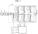
- Figure 1 is a diagram showing a configuration example of a general power conversion device to which the present invention is applicable.
- a power conversion device 102 is connected to an AC power system 101 through a transformer 104.
- the power conversion device 102 is connected to variable DC voltage source 103.
- the power conversion device 102 is configured by a DSMMC converter.
- the power conversion device 102 is configured by so-called Graetz connection of six sets of arms in which arm converters 105 and reactors 106 are connected in series.
- the power conversion device 102 includes six arm converters 105 (105UP, 105UN, 105VP, 105VN, 105WP, 105WN) each having two output terminals, a terminal a and a terminal b, and six circulating current suppression reactors 106 (106UP, 106UN, 106VP, 106VN, 106WP, 106WN).
- the power conversion device 102 includes six current detectors 107 (107UP, 107UN, 107VP, 107VN, 107WP, 107WN) for detecting arm currents I (I UP , I UN , I VP , I VN , I WP , and I WN ) of each phase in order to acquire control signals.
- a control device 108 detects and receives arm currents from six current detectors 107 and output AC voltages V G (V GU , V GV , V GW ) of the power conversion device 102 from the AC voltage detector 109, and provides a gate control signal g for the six arm converters 105.
- V G V GU , V GV , V GW
- the AC phases are represented by U, V, and W
- the positive and negative of a DC circuit are represented by PN.
- the notations of 3, 6, and 3N for various signal lines indicate the total number of signal lines described as one.
- the terminals b of the arm converters 105UP, 105VP, and 105WP on the positive side and the terminals a of the arm converters 105UN, 105VN, and 105WN on the negative side are connected to AC power supply terminals (terminal U, terminal V, terminal V) through the circulating current suppression reactors 106 (106UP, 106UN, 106VP, 106VN, 106WP, 106WN).
- the terminals a of the positive side arm converters 105UP, 105VP, and 105WP and the terminals b of the negative side arm converters 105UN, 105VN, and 105WN are connected to the positive and negative terminals (terminal P, terminal N) of DC.
- the variable DC voltage source 103 is also connected to the DC terminal.
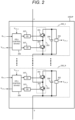
- FIG. 2 is a diagram showing a configuration example of a general arm converter to which the present invention is applicable.
- the arm converter 105UP will be described as a representative, but since the other arm converters 105UN, 105VP, 105VN, 105WP, and 105WN have the same configuration, the description of the other arm converters will be omitted.
- the arm converter 105UP is a circuit in which N unit converters 200 (200_1 to 200_N) are connected in series.
- the unit converter 200 is a case of using a half-bridge circuit, and N is the number of unit converters per arm converter.
- the unit converter 200 has a switching circuit 203 in which two switching elements 201 and 202 with freewheeling diodes connected in parallel are connected in series, a capacitor 204 as an energy storage element, and a voltage detector 205, which are connected in parallel.
- the unit converter 200 also has a cell control device 206 and two gate drive circuits 207. Terminals a and b in Figure 2 are output terminals of the arm converter 105UP and correspond to the terminals a and b of the arm converter in Figure 1 .
- the voltage detector 205 detects a capacitor voltage of each unit converter and transmits a detected capacitor voltage V C (V CUP_1 to V CUP_N ) to the cell control device 206 of each unit converter 200.
- the cell control device 206 distributes gate commands g (g UP_1 to g UP_N ) of the unit converter, which are sent from the control device 108 in Figure 1 to the gate drive circuit 207. Also, the cell control device 206 sends the capacitor voltages V CUP_1 to V CUP_N detected by voltage detector 205 to the control device 108.
- the gate drive circuit 207 generates a gate drive signal for switching on/off switching elements 201 and 202 in accordance with the gate command g, and supplies the signal to the switching elements 201 and 202.
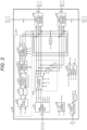
- FIG. 3 is a diagram showing a configuration example of a control device according to Example 1 of the present invention.
- the control device 108 receives arm currents I (I UP , I UN , I VP , I VN , I WP , I WN ) and all 6 ⁇ N unit converter capacitor voltages V C (V CUP_1 to V CUP_N , V CUN_1 to V CUN_N , V CVP_1 to V CVP_N , V CVN_1 to V CVN_N , V CWP_1 to V CWP_N , V CWN_1 to V CWN_N ) and output AC voltage V G (V GU , V GV , V GW ) , and outputs 6 ⁇ N gate commands g (g UP_1 to g UP_N , g UN_1 to g UN_N , g VP_1 to g VP_N , g VN_1 to g VN_N ,
- the control device 108 includes arm current separation means 301, AC current control means 302, DC current control means 303, circulating current control means 304, phase detection means 305, PWM command generation means 306 for the P-side arm converter, PWM command generation means 307 for the N-side arm converter, and coordinate transformation means 308.
- the present invention reflects the output of the circulating current control means 304 in the output of the AC current control means 302, as the target signals of the PWM command generation means (PWM & inter-cell balance control) 306 and 307 of the PN side arm converter).
- Other means 301, 303, 305, and 308 generate signals used in the processing executed in the present invention, and those internal processing has been known in Patent Literature 1 and Patent Literature 2, and therefore, only an outline of those means will be described here.
- the arm current separation means 301 receives arm currents I (I UP , I UN , I VP , I VN , I WP , I WN ) and generates AC currents I u , I v , l w , circulating currents I zu , I zv , I zw circulating between the upper and lower arms of the converters, and a DC current I DC .
- the circulating currents I zu , I zv , and I zw used in circulating current control means 304 can be obtained from the following Expressions (1), (2), and (3).
- I zu I UP + I UN / 2 ⁇ I DC / 3
- I zv I VP + I VN / 2 ⁇ I DC / 3
- I zw I WP + I WN / 2 ⁇ I DC / 3
- the DC current control means 303 receives the DC current I DC and its target current I DC * to generate a DC voltage target value V DC *.
- the phase detection means 305 receives output AC voltages V G (V GU , V GV , V Gw ) and generates phases ⁇ and 2 ⁇ .
- the coordinate transformation means 308 receives three-phase output AC voltages V G (V GU , V GV , V GW ), converts the received voltages into orthogonal two-axis coordinate voltages V ⁇ and V ⁇ , and receives three-phase circulating currents I zu , I zv , I zw and converts the received currents into orthogonal two-axis coordinate currents I ⁇ and I ⁇ .
- the AC current control means 302 transforms coordinate of the three-phase AC currents I u , I v , and l w into two-axis currents I ⁇ and I ⁇ with using a phase angle of ⁇ , and it operates to a difference between the two-axis currents and the target two-axis current values I ⁇ * and I ⁇ * which are preset through the respective current regulators. Further, the AC current control means 302 generates and outputs three-phase output AC voltage set values V G * (V GU *, V GV *, V GW *) by inverse coordinate transformation from two-axis to three-axis.
- the circulating current control means 304 which is a main circuit portion of the present invention, includes PQ calculation means 309, a filter circuit 310, power factor calculation means 311, circulating current command calculation means 312, and circulating current control means 313.
- the PQ calculation means 309 calculates an active power P and a reactive power Q output by the power conversion device 102 from output AC voltages V ⁇ and V ⁇ and the AC currents I ⁇ and I ⁇ obtained from the coordinate transformation means 308.
- the filter circuit 310 removes high-frequency components contained in the active power P and the reactive power Q.
- the power factor calculation means 311 calculates a power factor cos ⁇ from the active power P' and the reactive power Q', from which high frequency components have been removed, obtained from the filter circuit 310.
- the circulating current command calculation means 312 is means for calculating the circulating current commands I zu *, I zv *, I zw * of each phase using the power factor cos ⁇ as an input. A specific method of calculating the circulating current commands I zu *, I zv *, and I zw * will be described later.
- the circulating current control means 313 is means for causing the circulating currents I zu , I zv , and I zw of each phase to follow the circulating current commands I zu *, I zv *, and I zw *.
- the circulating current control means 313 includes a proportional controller or a proportional integral controller, and generates circulating voltage command values V ZU *, V ZV *, and V ZW * such that the circulating current of each phase follows the command value.
- Figure 4 is a diagram showing a configuration example of the circulating current command calculation means 312 according to Example 1 of the present invention.
- the circulating current command calculation means 312 of Figure 4 includes circulating current amplitude calculation means 401, circulating current phase calculation means 402, and a multiplier 403.
- Figure 5 is an input/output characteristic diagram of the circulating current amplitude calculation means 401 according to Example 1 of the present invention.
- the horizontal axis represents the power factor cos ⁇
- the vertical axis represents the current amplitude
- the power factor cos ⁇ calculated by Expression (6) cannot distinguish between the inductive and capacitive properties of the reactive power Q'. Therefore, the circulating current amplitude calculation means 401 receives the reactive power Q' as an input and determines whether it is inductive or capacitive based on the sign of Q'.
- the circulating current amplitude calculation means 401 has an input/output characteristic in which the current amplitude
- at the time of cos ⁇ 0 (inductive) decreases linearly to a power factor of 1 as a peak value.
- has constant input/output characteristics.
- the horizontal axis represents time, and the vertical axis represents the value of each voltage expressed in arbitrary units.
- the capacitor voltage V CUP_1 fluctuates around the voltage command value V C .
- the output voltage command V UP * is a voltage command value calculated by the control device so that a desired arm current I UP flows.
- a time at which the capacitor voltage V CUP_1 reaches a bottom value and a time at which the output voltage command V UP * reaches a peak value approximately match with each other.
- a maximum voltage that can be output from the power conversion device 102 also drops. That is, at a moment when the bottom value of the capacitor voltage V CUP_1 and the peak value of the output voltage command V UP * overlap with each other, an overmodulation operation mode is entered in which the output voltage command V UP * is greater than the maximum voltage that can be output by the power conversion device 102.
- Figures 6, 7 , and 8 exemplify the capacitor voltage V CUP_1 of the U-phase first unit converter and the U-phase output voltage command V UP *, but a similar description can be applied to other phases.
- FIG. 9 is a diagram showing a relationship between the phase compensation element ⁇ c and the peak value of the output voltage command V UP *.
- the horizontal axis represents the phase compensation element ⁇ c
- the vertical axis represents the peak value of the output voltage command V UP * expressed in arbitrary units. From Figure 9 , in order to effectively reduce the peak value of the output voltage command V UP *, the phase compensation element ⁇ c should be set to ⁇ (rad) .
- the circulating current control means 313 generates the circulating voltage target values V zu *, V zv *, and V zw * as a result of proportional integral processing on differences between the circulating current commands I zu *, I zv *, and I zw * and the circulating currents I ZU , I zv , and I ZW derived by the arm current separation means 301 in a regulator, to resultantly generate the circulating voltage target values V zu *, V zv *, and V zw *.
- the PWM command generation means 306 of the P-side arm converter and the PWM command generation means 307 of the N-side arm converter are supplied with addition signals of the Vow three-phase output AC voltage set values V U *, V V *, and V W * generated by the AC current control means 302 and the circulating voltage target values V zu *, V zv *, and V zw * generated by the circulating current control means 304 (in the means 306, V UP *, V Vp *, V Wp *, and in the means 307, V UN *, V VN *, V WN *) as the voltage target signals, respectively.
- the PWM command generation means 306 of the P-side arm converter and the PWM command generation means 307 of the N-side arm converter generate gate signals to be given to each positive and negative arm and each unit converter 200 in each arm, and controls the gate signals.
- the output of the circulating current control means 304 is reflected in the output of the AC current control means 302 to obtain a target signal of the PWM command generation means 306 and 307 of the PN side arm converter.
- the circulating current is controlled according to the power factor.
- Figures 10 and 11 show examples of operating waveforms before and after application of the circulating current command calculation means 312 of the present invention.
- the left side of Figure 10 is before application of the circulating current command calculation means 312, and the right side of Figure 10 is after applying the circulating current command calculation means 312.
- the left and right upper rows are the capacitor voltage V CUP_1 and the output voltage command V UP *, and the left and right lower rows are the circulating current command I zu *.
- the bottom value of the capacitor voltage V CUP_1 and the peak value of the output voltage command V UP * approximately match with each other.
- the circulating current shown in the present example reduces the voltage fluctuation of the capacitor voltage V CUP_1 and the output voltage command V UP * can be prevented from overlapping with the bottom value of the capacitor voltage V CUP_1 .
- the circulating current shown in the present invention can reduce the peak value of the output voltage command V UP *.
- the left side of Figure 11 is before application of the circulating current command calculation means 312, and the right side of Figure 11 is after application of the circulating current command calculation means 312.
- the upper left and right sides of Figure 11 are the capacitor voltage V CUP_1 and the output voltage command V UP *, and the lower left and right sides of Figure 11 are the circulating current command I zu *.
- the voltage command value V C of the capacitor voltage V CUP_1 and the peak value of the output voltage command V UP * approximately match with each other.
- the value of the capacitor voltage V CUP_1 can be shifted above the command value V C at the peak of the output voltage command V UP * by allowing the circulating current shown in the present example to flow.
- the peak value of the output voltage command V UP * can be reduced by applying the circulating current command calculation means 312.
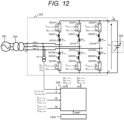
- FIG. 12 is a diagram showing a configuration example of a power conversion device according to Example 2 of the present invention.
- the signs in the figure that overlap with those in Figure 1 have the same meanings, so that descriptions thereof will be omitted, but the main circuit configuration remains as it is, and the control device side is changed.
- Figure 12 differs from Figure 1 of Example 1 in that a power factor command cos ⁇ * sent from the host control device 1201 to the control device 108 is input to the control device 108, and there is provided an interface for sending the power factor command cos ⁇ * from the host control device 1201 to the control device 108.
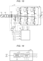
- FIG. 13 Another configuration example of the power conversion device according to Example 2 in Figure 13 differs from Figure 1 of Example 1 in that an AC current detector 1301 and a power factor detector 1302 are newly provided and that there is provided an interface for sending the power factor cos ⁇ detected by the power factor detector 1302 to the control device 108.
- Figure 14 is a diagram showing a configuration example of circulating current command calculation means according to Example 2 of the present invention.
- the PQ calculation means 309, the filter circuit 310, and the power factor calculation means 311 in the circulating current control means 304 are unnecessary.
- a power conversion device using an inexpensive microcomputer since a calculation time can be reduced by reducing the number of calculation means in the control device.
- FIG 15 is a diagram showing a configuration example of circulating current command calculation means according to Example 3 of the present invention.
- the signs in the figure that overlap with those in Figure 4 have the same meanings, so that descriptions thereof will be omitted.
- Circulating current command calculation means 312 in Figure 15 differs from Example 1 of Figure 4 in that there is provided a time constant calculation means 1501. Also, circulating current amplitude calculation means 1502 is different.
- the time constant calculation means 1501 calculates a time constant ⁇ for inputs of active power P', the number N of unit converters per arm converter, a voltage command value VC of the capacitor voltage, and a capacitance C of the capacitor.
- Figure 16 is an input/output characteristic diagram of the circulating current amplitude calculation means according to Example 3 of the present invention.
- the circulating current amplitude calculation means 1502 of Example 3 differs from Example 1 in that the circulating current amplitude can be selected according to a value of the time constant.
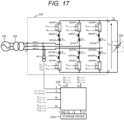
- Figure 17 is a circuit diagram showing another configuration example of the circulating current amplitude calculation means according to Example 3 of the present invention.
- Figure 17 differs from Figure 1 of Example 1 in that there are provided a storage device 1701 and an interface necessary for exchanging input/output signals between the storage device 1701 and the control device 108.
- the storage device 1701 is, for example, a device such as a register, flash memory, or hard disk drive that saves and stores data.
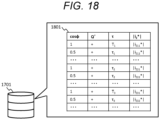
- Figure 18 shows a storage device according to Example 3 of the present invention.
- Figure 19 is a block diagram of circulating current command calculation means according to Example 3 of the present invention.
- the storage device 1701 has a database 1801 inside, and selects, from the database 1801, a circulating current amplitude
- the circulating current amplitude can be automatically adjusted according to a change in the time constant ⁇ . Therefore, a power conversion device that can select an optimum circulating current for each operating condition can be provided.
- 101 power system
- 102 power conversion device
- 103 variable DC voltage source
- 104 transformer
- 105UP, 105UN, 105VP, 105VN, 105WP, 105WN arm converter
- 106UP, 106UN, 106VP, 106VN, 106WP, 106WN circulating current suppression reactor
- 107UP, 107UN, 107VP, 107VN, 107WP, 107WN current detector
- 108 control device, 109: AC voltage detector
- 203 switching circuit
- 204 capacitor
- 205 DC voltage detector
- 206 cell control device
- 207 gate drive circuit
- 301 arm current separation means
- 302 AC current control means
- 304 circulating current control means
- 305 phase detection means
- 306 PWM command generation means
- 308 coordinate transformation means
- 310 filter circuit
- 311 power factor calculation means
- 312 circulating current suppression reactor
Landscapes
- Engineering & Computer Science (AREA)
- Power Engineering (AREA)
- Inverter Devices (AREA)
Applications Claiming Priority (2)
| Application Number | Priority Date | Filing Date | Title |
|---|---|---|---|
| JP2020090327A JP2021185727A (ja) | 2020-05-25 | 2020-05-25 | 電力変換装置の制御装置及び制御方法 |
| PCT/JP2021/015556 WO2021241054A1 (ja) | 2020-05-25 | 2021-04-15 | 電力変換装置の制御装置及び制御方法 |
Publications (2)
| Publication Number | Publication Date |
|---|---|
| EP4160901A1 true EP4160901A1 (de) | 2023-04-05 |
| EP4160901A4 EP4160901A4 (de) | 2024-07-10 |
Family
ID=78744300
Family Applications (1)
| Application Number | Title | Priority Date | Filing Date |
|---|---|---|---|
| EP21812217.4A Withdrawn EP4160901A4 (de) | 2020-05-25 | 2021-04-15 | Steuerungsvorrichtung und steuerungsverfahren für eine leistungsumwandlungsvorrichtung |
Country Status (3)
| Country | Link |
|---|---|
| EP (1) | EP4160901A4 (de) |
| JP (1) | JP2021185727A (de) |
| WO (1) | WO2021241054A1 (de) |
Families Citing this family (2)
| Publication number | Priority date | Publication date | Assignee | Title |
|---|---|---|---|---|
| WO2024134858A1 (ja) * | 2022-12-23 | 2024-06-27 | 三菱電機株式会社 | 電力変換装置 |
| CN117833642B (zh) * | 2024-01-07 | 2024-11-12 | 国网江西省电力有限公司九江供电分公司 | 一种模块化多电dc/dc变换器控制方法 |
Family Cites Families (9)
| Publication number | Priority date | Publication date | Assignee | Title |
|---|---|---|---|---|
| JP4164428B2 (ja) * | 2003-10-02 | 2008-10-15 | 三井造船株式会社 | 誘導加熱用並列インバータの給電方法および誘導加熱用並列型インバータ装置 |
| CA2671817C (en) * | 2006-12-08 | 2016-09-13 | Siemens Aktiengesellschaft | Control of a modular converter with distributed energy stores |
| JP5721096B2 (ja) * | 2010-08-23 | 2015-05-20 | 国立大学法人東京工業大学 | 電力変換器 |
| JP5865104B2 (ja) * | 2012-02-09 | 2016-02-17 | 株式会社日立製作所 | 電圧型電力変換器の電流制御装置及び電圧型電力変換器の電流制御方法 |
| EP2645552B1 (de) * | 2012-02-09 | 2020-04-22 | Hitachi, Ltd. | Schaltelement, Stromrichter, Gleichstromübertragungssystem, Stromsteuervorrichtung, Verfahren zur Steuerung eines Stromrichters, und Verfahren zur Steuerung des Stroms in einem spannungsgespeisten Umrichter |
| JP6131030B2 (ja) * | 2012-03-21 | 2017-05-17 | 株式会社日立製作所 | 単位変換器、電力変換装置、直流送電システム、および、電力変換装置の制御方法 |
| JP5827924B2 (ja) | 2012-05-30 | 2015-12-02 | 株式会社日立製作所 | 電圧型電力変換装置の制御装置及び制御方法 |
| KR20160072499A (ko) * | 2014-12-15 | 2016-06-23 | 엘에스산전 주식회사 | 모듈형 멀티 레벨 컨버터의 운전 방법 |
| JP6957196B2 (ja) * | 2017-05-17 | 2021-11-02 | 株式会社東芝 | 電力変換装置 |
-
2020
- 2020-05-25 JP JP2020090327A patent/JP2021185727A/ja active Pending
-
2021
- 2021-04-15 EP EP21812217.4A patent/EP4160901A4/de not_active Withdrawn
- 2021-04-15 WO PCT/JP2021/015556 patent/WO2021241054A1/ja not_active Ceased
Also Published As
| Publication number | Publication date |
|---|---|
| JP2021185727A (ja) | 2021-12-09 |
| WO2021241054A1 (ja) | 2021-12-02 |
| EP4160901A4 (de) | 2024-07-10 |
Similar Documents
| Publication | Publication Date | Title |
|---|---|---|
| US8154893B2 (en) | Three-phase power converting apparatus | |
| US4729082A (en) | Control device for power converter | |
| US6741482B2 (en) | Power conversion device | |
| US8228699B2 (en) | Power converting apparatus including half-bridge inverters connected between positive and negative terminals of a DC power supply | |
| JP6180641B2 (ja) | 電力変換装置 | |
| CN105048788B (zh) | 一种混合级联结构的多端口电力电子变压器及其控制方法 | |
| CN103441512B (zh) | 基于模块化多电平变流器的无功补偿(mmc-statcom)方法 | |
| CN112165244A (zh) | 一种主从式并联逆变器输出均流控制方法 | |
| CN102047545A (zh) | 矩阵变换器的控制装置及其输出电压产生方法 | |
| JP6752401B1 (ja) | 電力変換装置 | |
| EP4131765A1 (de) | Leistungswandler | |
| EP4160901A1 (de) | Steuerungsvorrichtung und steuerungsverfahren für eine leistungsumwandlungsvorrichtung | |
| CN115000978A (zh) | 一种h桥级联型statcom直流侧电压二倍频波动抑制方法 | |
| JP6818956B1 (ja) | 電力変換装置 | |
| CN112087158A (zh) | 一种模块化多电平变换器的开环环流抑制方法 | |
| CN117318190B (zh) | 一种下垂控制并联逆变器自适应虚拟阻抗调节方法 | |
| JP6771707B1 (ja) | 電力変換装置 | |
| JP4365171B2 (ja) | 電力変換装置及びそれを用いたパワーコンディショナ | |
| CN107947623A (zh) | 一种负载不平衡条件下双向ac/dc变换器的多模态自治运行控制方法 | |
| WO2019049713A1 (ja) | 電力変換装置およびその制御方法 | |
| CN111817365B (zh) | 适用于超大规模储能的模块化多回路变流器控制方法 | |
| CN111404412B (zh) | 一种模块化多电平变换器直流电容选取方法及装置 | |
| JP7166507B1 (ja) | 電力変換装置 | |
| RU2682164C1 (ru) | Устройство управления высоковольтным преобразователем частоты | |
| CN118889539A (zh) | 一种三相燃料电池并网系统功率控制方法及相关装置 |
Legal Events
| Date | Code | Title | Description |
|---|---|---|---|
| STAA | Information on the status of an ep patent application or granted ep patent |
Free format text: STATUS: THE INTERNATIONAL PUBLICATION HAS BEEN MADE |
|
| PUAI | Public reference made under article 153(3) epc to a published international application that has entered the european phase |
Free format text: ORIGINAL CODE: 0009012 |
|
| STAA | Information on the status of an ep patent application or granted ep patent |
Free format text: STATUS: REQUEST FOR EXAMINATION WAS MADE |
|
| 17P | Request for examination filed |
Effective date: 20221115 |
|
| AK | Designated contracting states |
Kind code of ref document: A1 Designated state(s): AL AT BE BG CH CY CZ DE DK EE ES FI FR GB GR HR HU IE IS IT LI LT LU LV MC MK MT NL NO PL PT RO RS SE SI SK SM TR |
|
| DAV | Request for validation of the european patent (deleted) | ||
| DAX | Request for extension of the european patent (deleted) | ||
| REG | Reference to a national code |
Ref country code: DE Ref legal event code: R079 Free format text: PREVIOUS MAIN CLASS: H02M0007490000 Ipc: H02M0007483000 |
|
| A4 | Supplementary search report drawn up and despatched |
Effective date: 20240606 |
|
| RIC1 | Information provided on ipc code assigned before grant |
Ipc: H02M 1/12 20060101ALI20240531BHEP Ipc: H02M 1/08 20060101ALI20240531BHEP Ipc: H02M 7/5395 20060101ALI20240531BHEP Ipc: H02M 7/5387 20070101ALI20240531BHEP Ipc: H02M 7/483 20070101AFI20240531BHEP |
|
| STAA | Information on the status of an ep patent application or granted ep patent |
Free format text: STATUS: THE APPLICATION IS DEEMED TO BE WITHDRAWN |
|
| 18D | Application deemed to be withdrawn |
Effective date: 20241101 |