EP4159704B1 - Kupfer/keramik-verbundkörper und isoliertes schaltungssubstrat - Google Patents
Kupfer/keramik-verbundkörper und isoliertes schaltungssubstrat Download PDFInfo
- Publication number
- EP4159704B1 EP4159704B1 EP21813874.1A EP21813874A EP4159704B1 EP 4159704 B1 EP4159704 B1 EP 4159704B1 EP 21813874 A EP21813874 A EP 21813874A EP 4159704 B1 EP4159704 B1 EP 4159704B1
- Authority
- EP
- European Patent Office
- Prior art keywords
- copper
- ceramic
- ceramic substrate
- layer
- bonding
- Prior art date
- Legal status (The legal status is an assumption and is not a legal conclusion. Google has not performed a legal analysis and makes no representation as to the accuracy of the status listed.)
- Active
Links
Images


Classifications
-
- C—CHEMISTRY; METALLURGY
- C04—CEMENTS; CONCRETE; ARTIFICIAL STONE; CERAMICS; REFRACTORIES
- C04B—LIME, MAGNESIA; SLAG; CEMENTS; COMPOSITIONS THEREOF, e.g. MORTARS, CONCRETE OR LIKE BUILDING MATERIALS; ARTIFICIAL STONE; CERAMICS; REFRACTORIES; TREATMENT OF NATURAL STONE
- C04B37/00—Joining burned ceramic articles with other burned ceramic articles or other articles by heating
- C04B37/02—Joining burned ceramic articles with other burned ceramic articles or other articles by heating with metallic articles
- C04B37/023—Joining burned ceramic articles with other burned ceramic articles or other articles by heating with metallic articles characterised by the interlayer used
- C04B37/026—Joining burned ceramic articles with other burned ceramic articles or other articles by heating with metallic articles characterised by the interlayer used consisting of metals or metal salts
-
- H—ELECTRICITY
- H10—SEMICONDUCTOR DEVICES; ELECTRIC SOLID-STATE DEVICES NOT OTHERWISE PROVIDED FOR
- H10W—GENERIC PACKAGES, INTERCONNECTIONS, CONNECTORS OR OTHER CONSTRUCTIONAL DETAILS OF DEVICES COVERED BY CLASS H10
- H10W40/00—Arrangements for thermal protection or thermal control
- H10W40/20—Arrangements for cooling
- H10W40/25—Arrangements for cooling characterised by their materials
- H10W40/255—Arrangements for cooling characterised by their materials having a laminate or multilayered structure, e.g. direct bond copper [DBC] ceramic substrates
-
- C—CHEMISTRY; METALLURGY
- C04—CEMENTS; CONCRETE; ARTIFICIAL STONE; CERAMICS; REFRACTORIES
- C04B—LIME, MAGNESIA; SLAG; CEMENTS; COMPOSITIONS THEREOF, e.g. MORTARS, CONCRETE OR LIKE BUILDING MATERIALS; ARTIFICIAL STONE; CERAMICS; REFRACTORIES; TREATMENT OF NATURAL STONE
- C04B37/00—Joining burned ceramic articles with other burned ceramic articles or other articles by heating
- C04B37/02—Joining burned ceramic articles with other burned ceramic articles or other articles by heating with metallic articles
-
- C—CHEMISTRY; METALLURGY
- C04—CEMENTS; CONCRETE; ARTIFICIAL STONE; CERAMICS; REFRACTORIES
- C04B—LIME, MAGNESIA; SLAG; CEMENTS; COMPOSITIONS THEREOF, e.g. MORTARS, CONCRETE OR LIKE BUILDING MATERIALS; ARTIFICIAL STONE; CERAMICS; REFRACTORIES; TREATMENT OF NATURAL STONE
- C04B35/00—Shaped ceramic products characterised by their composition; Ceramics compositions; Processing powders of inorganic compounds preparatory to the manufacturing of ceramic products
- C04B35/622—Forming processes; Processing powders of inorganic compounds preparatory to the manufacturing of ceramic products
- C04B35/64—Burning or sintering processes
- C04B35/645—Pressure sintering
-
- C—CHEMISTRY; METALLURGY
- C04—CEMENTS; CONCRETE; ARTIFICIAL STONE; CERAMICS; REFRACTORIES
- C04B—LIME, MAGNESIA; SLAG; CEMENTS; COMPOSITIONS THEREOF, e.g. MORTARS, CONCRETE OR LIKE BUILDING MATERIALS; ARTIFICIAL STONE; CERAMICS; REFRACTORIES; TREATMENT OF NATURAL STONE
- C04B37/00—Joining burned ceramic articles with other burned ceramic articles or other articles by heating
- C04B37/02—Joining burned ceramic articles with other burned ceramic articles or other articles by heating with metallic articles
- C04B37/021—Joining burned ceramic articles with other burned ceramic articles or other articles by heating with metallic articles in a direct manner, e.g. direct copper bonding [DCB]
-
- H—ELECTRICITY
- H05—ELECTRIC TECHNIQUES NOT OTHERWISE PROVIDED FOR
- H05K—PRINTED CIRCUITS; CASINGS OR CONSTRUCTIONAL DETAILS OF ELECTRIC APPARATUS; MANUFACTURE OF ASSEMBLAGES OF ELECTRICAL COMPONENTS
- H05K1/00—Printed circuits
- H05K1/02—Details
-
- H—ELECTRICITY
- H05—ELECTRIC TECHNIQUES NOT OTHERWISE PROVIDED FOR
- H05K—PRINTED CIRCUITS; CASINGS OR CONSTRUCTIONAL DETAILS OF ELECTRIC APPARATUS; MANUFACTURE OF ASSEMBLAGES OF ELECTRICAL COMPONENTS
- H05K1/00—Printed circuits
- H05K1/02—Details
- H05K1/03—Use of materials for the substrate
- H05K1/0306—Inorganic insulating substrates, e.g. ceramic, glass
-
- H—ELECTRICITY
- H05—ELECTRIC TECHNIQUES NOT OTHERWISE PROVIDED FOR
- H05K—PRINTED CIRCUITS; CASINGS OR CONSTRUCTIONAL DETAILS OF ELECTRIC APPARATUS; MANUFACTURE OF ASSEMBLAGES OF ELECTRICAL COMPONENTS
- H05K3/00—Apparatus or processes for manufacturing printed circuits
- H05K3/38—Improvement of the adhesion between the insulating substrate and the metal
- H05K3/388—Improvement of the adhesion between the insulating substrate and the metal by the use of a metallic or inorganic thin film adhesion layer
-
- C—CHEMISTRY; METALLURGY
- C04—CEMENTS; CONCRETE; ARTIFICIAL STONE; CERAMICS; REFRACTORIES
- C04B—LIME, MAGNESIA; SLAG; CEMENTS; COMPOSITIONS THEREOF, e.g. MORTARS, CONCRETE OR LIKE BUILDING MATERIALS; ARTIFICIAL STONE; CERAMICS; REFRACTORIES; TREATMENT OF NATURAL STONE
- C04B2235/00—Aspects relating to ceramic starting mixtures or sintered ceramic products
- C04B2235/65—Aspects relating to heat treatments of ceramic bodies such as green ceramics or pre-sintered ceramics, e.g. burning, sintering or melting processes
- C04B2235/656—Aspects relating to heat treatments of ceramic bodies such as green ceramics or pre-sintered ceramics, e.g. burning, sintering or melting processes characterised by specific heating conditions during heat treatment
- C04B2235/6567—Treatment time
-
- C—CHEMISTRY; METALLURGY
- C04—CEMENTS; CONCRETE; ARTIFICIAL STONE; CERAMICS; REFRACTORIES
- C04B—LIME, MAGNESIA; SLAG; CEMENTS; COMPOSITIONS THEREOF, e.g. MORTARS, CONCRETE OR LIKE BUILDING MATERIALS; ARTIFICIAL STONE; CERAMICS; REFRACTORIES; TREATMENT OF NATURAL STONE
- C04B2235/00—Aspects relating to ceramic starting mixtures or sintered ceramic products
- C04B2235/65—Aspects relating to heat treatments of ceramic bodies such as green ceramics or pre-sintered ceramics, e.g. burning, sintering or melting processes
- C04B2235/658—Atmosphere during thermal treatment
- C04B2235/6581—Total pressure below 1 atmosphere, e.g. vacuum
-
- C—CHEMISTRY; METALLURGY
- C04—CEMENTS; CONCRETE; ARTIFICIAL STONE; CERAMICS; REFRACTORIES
- C04B—LIME, MAGNESIA; SLAG; CEMENTS; COMPOSITIONS THEREOF, e.g. MORTARS, CONCRETE OR LIKE BUILDING MATERIALS; ARTIFICIAL STONE; CERAMICS; REFRACTORIES; TREATMENT OF NATURAL STONE
- C04B2235/00—Aspects relating to ceramic starting mixtures or sintered ceramic products
- C04B2235/65—Aspects relating to heat treatments of ceramic bodies such as green ceramics or pre-sintered ceramics, e.g. burning, sintering or melting processes
- C04B2235/66—Specific sintering techniques, e.g. centrifugal sintering
- C04B2235/661—Multi-step sintering
-
- C—CHEMISTRY; METALLURGY
- C04—CEMENTS; CONCRETE; ARTIFICIAL STONE; CERAMICS; REFRACTORIES
- C04B—LIME, MAGNESIA; SLAG; CEMENTS; COMPOSITIONS THEREOF, e.g. MORTARS, CONCRETE OR LIKE BUILDING MATERIALS; ARTIFICIAL STONE; CERAMICS; REFRACTORIES; TREATMENT OF NATURAL STONE
- C04B2237/00—Aspects relating to ceramic laminates or to joining of ceramic articles with other articles by heating
- C04B2237/02—Aspects relating to interlayers, e.g. used to join ceramic articles with other articles by heating
- C04B2237/12—Metallic interlayers
-
- C—CHEMISTRY; METALLURGY
- C04—CEMENTS; CONCRETE; ARTIFICIAL STONE; CERAMICS; REFRACTORIES
- C04B—LIME, MAGNESIA; SLAG; CEMENTS; COMPOSITIONS THEREOF, e.g. MORTARS, CONCRETE OR LIKE BUILDING MATERIALS; ARTIFICIAL STONE; CERAMICS; REFRACTORIES; TREATMENT OF NATURAL STONE
- C04B2237/00—Aspects relating to ceramic laminates or to joining of ceramic articles with other articles by heating
- C04B2237/02—Aspects relating to interlayers, e.g. used to join ceramic articles with other articles by heating
- C04B2237/12—Metallic interlayers
- C04B2237/122—Metallic interlayers based on refractory metals
-
- C—CHEMISTRY; METALLURGY
- C04—CEMENTS; CONCRETE; ARTIFICIAL STONE; CERAMICS; REFRACTORIES
- C04B—LIME, MAGNESIA; SLAG; CEMENTS; COMPOSITIONS THEREOF, e.g. MORTARS, CONCRETE OR LIKE BUILDING MATERIALS; ARTIFICIAL STONE; CERAMICS; REFRACTORIES; TREATMENT OF NATURAL STONE
- C04B2237/00—Aspects relating to ceramic laminates or to joining of ceramic articles with other articles by heating
- C04B2237/02—Aspects relating to interlayers, e.g. used to join ceramic articles with other articles by heating
- C04B2237/12—Metallic interlayers
- C04B2237/126—Metallic interlayers wherein the active component for bonding is not the largest fraction of the interlayer
- C04B2237/127—The active component for bonding being a refractory metal
-
- C—CHEMISTRY; METALLURGY
- C04—CEMENTS; CONCRETE; ARTIFICIAL STONE; CERAMICS; REFRACTORIES
- C04B—LIME, MAGNESIA; SLAG; CEMENTS; COMPOSITIONS THEREOF, e.g. MORTARS, CONCRETE OR LIKE BUILDING MATERIALS; ARTIFICIAL STONE; CERAMICS; REFRACTORIES; TREATMENT OF NATURAL STONE
- C04B2237/00—Aspects relating to ceramic laminates or to joining of ceramic articles with other articles by heating
- C04B2237/30—Composition of layers of ceramic laminates or of ceramic or metallic articles to be joined by heating, e.g. Si substrates
- C04B2237/32—Ceramic
- C04B2237/36—Non-oxidic
- C04B2237/366—Aluminium nitride
-
- C—CHEMISTRY; METALLURGY
- C04—CEMENTS; CONCRETE; ARTIFICIAL STONE; CERAMICS; REFRACTORIES
- C04B—LIME, MAGNESIA; SLAG; CEMENTS; COMPOSITIONS THEREOF, e.g. MORTARS, CONCRETE OR LIKE BUILDING MATERIALS; ARTIFICIAL STONE; CERAMICS; REFRACTORIES; TREATMENT OF NATURAL STONE
- C04B2237/00—Aspects relating to ceramic laminates or to joining of ceramic articles with other articles by heating
- C04B2237/30—Composition of layers of ceramic laminates or of ceramic or metallic articles to be joined by heating, e.g. Si substrates
- C04B2237/32—Ceramic
- C04B2237/36—Non-oxidic
- C04B2237/368—Silicon nitride
-
- C—CHEMISTRY; METALLURGY
- C04—CEMENTS; CONCRETE; ARTIFICIAL STONE; CERAMICS; REFRACTORIES
- C04B—LIME, MAGNESIA; SLAG; CEMENTS; COMPOSITIONS THEREOF, e.g. MORTARS, CONCRETE OR LIKE BUILDING MATERIALS; ARTIFICIAL STONE; CERAMICS; REFRACTORIES; TREATMENT OF NATURAL STONE
- C04B2237/00—Aspects relating to ceramic laminates or to joining of ceramic articles with other articles by heating
- C04B2237/30—Composition of layers of ceramic laminates or of ceramic or metallic articles to be joined by heating, e.g. Si substrates
- C04B2237/40—Metallic
- C04B2237/407—Copper
-
- C—CHEMISTRY; METALLURGY
- C04—CEMENTS; CONCRETE; ARTIFICIAL STONE; CERAMICS; REFRACTORIES
- C04B—LIME, MAGNESIA; SLAG; CEMENTS; COMPOSITIONS THEREOF, e.g. MORTARS, CONCRETE OR LIKE BUILDING MATERIALS; ARTIFICIAL STONE; CERAMICS; REFRACTORIES; TREATMENT OF NATURAL STONE
- C04B2237/00—Aspects relating to ceramic laminates or to joining of ceramic articles with other articles by heating
- C04B2237/50—Processing aspects relating to ceramic laminates or to the joining of ceramic articles with other articles by heating
- C04B2237/58—Forming a gradient in composition or in properties across the laminate or the joined articles
-
- C—CHEMISTRY; METALLURGY
- C04—CEMENTS; CONCRETE; ARTIFICIAL STONE; CERAMICS; REFRACTORIES
- C04B—LIME, MAGNESIA; SLAG; CEMENTS; COMPOSITIONS THEREOF, e.g. MORTARS, CONCRETE OR LIKE BUILDING MATERIALS; ARTIFICIAL STONE; CERAMICS; REFRACTORIES; TREATMENT OF NATURAL STONE
- C04B2237/00—Aspects relating to ceramic laminates or to joining of ceramic articles with other articles by heating
- C04B2237/50—Processing aspects relating to ceramic laminates or to the joining of ceramic articles with other articles by heating
- C04B2237/60—Forming at the joining interface or in the joining layer specific reaction phases or zones, e.g. diffusion of reactive species from the interlayer to the substrate or from a substrate to the joining interface, carbide forming at the joining interface
-
- C—CHEMISTRY; METALLURGY
- C04—CEMENTS; CONCRETE; ARTIFICIAL STONE; CERAMICS; REFRACTORIES
- C04B—LIME, MAGNESIA; SLAG; CEMENTS; COMPOSITIONS THEREOF, e.g. MORTARS, CONCRETE OR LIKE BUILDING MATERIALS; ARTIFICIAL STONE; CERAMICS; REFRACTORIES; TREATMENT OF NATURAL STONE
- C04B2237/00—Aspects relating to ceramic laminates or to joining of ceramic articles with other articles by heating
- C04B2237/50—Processing aspects relating to ceramic laminates or to the joining of ceramic articles with other articles by heating
- C04B2237/70—Forming laminates or joined articles comprising layers of a specific, unusual thickness
-
- H—ELECTRICITY
- H10—SEMICONDUCTOR DEVICES; ELECTRIC SOLID-STATE DEVICES NOT OTHERWISE PROVIDED FOR
- H10W—GENERIC PACKAGES, INTERCONNECTIONS, CONNECTORS OR OTHER CONSTRUCTIONAL DETAILS OF DEVICES COVERED BY CLASS H10
- H10W90/00—Package configurations
- H10W90/701—Package configurations characterised by the relative positions of pads or connectors relative to package parts
- H10W90/731—Package configurations characterised by the relative positions of pads or connectors relative to package parts of die-attach connectors
- H10W90/734—Package configurations characterised by the relative positions of pads or connectors relative to package parts of die-attach connectors between a chip and a stacked insulating package substrate, interposer or RDL
Definitions
- This invention relates to a copper/ceramic bonded body formed by bonding a copper member, which is formed of copper or a copper alloy, and a ceramic member, as well as an insulated circuit substrate formed by bonding a copper sheet formed of copper or a copper alloy to the surface of a ceramic substrate.
- thermoelectric modules there are structures in which power semiconductor elements, LED elements, and thermoelectric elements are bonded with an insulated circuit substrate on which a circuit layer formed of a conductive material is formed on one surface of an insulating layer.
- insulated circuit substrates provided with a ceramic substrate formed of silicon nitride or the like, and a circuit layer formed by bonding a metal sheet with excellent electrical conductivity to one surface of the ceramic substrate are widely used in the related art.
- insulated circuit substrates on which a metal layer is formed by bonding a metal sheet to the other surface of the ceramic substrate are also insulated circuit substrates on which a metal layer is formed by bonding a metal sheet to the other surface of the ceramic substrate.
- Patent Document 1 proposes an insulated circuit substrate in which a circuit layer and a metal layer are formed by bonding copper sheets to one surface and the other surface of a ceramic substrate.
- copper sheets are arranged to interpose an Ag-Cu-Ti-based brazing material on one surface and the other surface of the ceramic substrate and the copper sheets are bonded by performing a heat treatment (the so-called active metal brazing method).
- Patent Document 2 proposes an insulated circuit substrate in which a copper sheet formed of copper or a copper alloy is bonded with the surface of a ceramic substrate formed of silicon nitride.
- an active metal and a Mg are arranged between the copper sheet and the ceramic substrate and the ceramic substrate and the copper sheet are bonded by heating the copper sheet and the ceramic substrate in a state of being pressed in the laminating direction.
- Patent Document 3 discloses a copper/ceramic joined body in which a copper member made of copper or a copper alloy and a ceramic member made of silicon nitride are joined.
- a compound layer of an active metal (Ti) is formed at the bonded interface between the ceramic substrate and the copper sheet.
- a TiN layer is formed at the bonded interface between the ceramic substrate and the copper sheet.
- an active metal nitride layer including one or two or more active metal nitrides selected from Ti, Zr, Nb, and Hf is formed on the ceramic substrate side between the copper sheet and the ceramic substrate.
- the insulated circuit substrate described above when a terminal material or the like was ultrasonically welded with the surface of the circuit layer (copper sheet), there were concerns that the copper sheet may be plastically deformed, the active metal nitride layer, such as the hard TiN layer, may be destroyed, and the bonding reliability may be decreased. In addition, there was a concern that breaking starting from the destruction of the TiN layer may occur in the ceramic substrate.
- This invention was created in consideration of circumstances described above and has an objective of providing a copper/ceramic bonded body in which a copper member, which is formed of copper or a copper alloy, and a ceramic member are reliably bonded and in which the bonding reliability is excellent even when ultrasonic waves are applied thereto, as well as an insulated circuit substrate.
- the crystal grains of the copper sheet are coarsened.
- an active metal nitride layer such as a TiN layer
- the region in the vicinity of the bonded interface of the copper sheet is easily deformed when ultrasonic waves are applied thereto and active metal nitride layers such as a TiN layer are destroyed.
- a copper/ceramic bonded body of an aspect of the present invention is a copper/ceramic bonded body formed by bonding a copper member, which is formed of copper or a copper alloy, and a ceramic member, in which, a ratio D1/D0 is 0.60 or less, D0 being an average crystal grain size of the entire copper member, D1 being an average crystal grain size of the copper member at a position 50 ⁇ m from a bonding surface with the ceramic member, D0 and D1 being obtained by observing a cross-section of the copper member along a laminating direction.
- a ratio D1/D0 of an average crystal grain size D1 at a position of 50 ⁇ m in the laminating direction from the bonding surface between the copper member and the ceramic member to an average crystal grain size D0 of the entire copper member is 0.60 or less, thus, the crystal grain size in the vicinity of the bonded interface is suppressed to be comparatively small, it is possible to suppress deformation of the copper member in the region in the vicinity of the bonded interface when ultrasonic waves are applied thereto, and it is possible to suppress the destruction of the active metal nitride layer such as a TiN layer.
- the crystal grain size is not significantly different between the entire copper member and in the vicinity of the bonded interface and it is possible to suppress the hardening of the entire copper member.
- Mg is diffused in a region in the copper member, the region being at least 50 ⁇ m from the bonding surface with the ceramic member in the laminating direction, and Mg concentration decreases with increasing a distance from the bonding surface.
- Mg is sufficiently diffused in a region of the copper member from the bonding surface with the ceramic member to at least 50 ⁇ m in the laminating direction and it is possible to make the crystal grain size in the vicinity of the bonded interface comparatively small.
- An insulated circuit substrate of an aspect of the present invention is an insulated circuit substrate formed by bonding a copper sheet, which is formed of copper or a copper alloy, with a surface of a ceramic substrate, in which, a ratio D1/D0 is 0.60 or less, D0 being an average crystal grain size of the entire copper sheet, D1 being an average crystal grain size of the copper sheet at a position 50 ⁇ m from a bonding surface with the ceramic substrate, D0 and D1 being obtained by observing a cross-section of the copper sheet along a laminating direction.
- a ratio D1/D0 of an average crystal grain size D1 at a position of 50 ⁇ m in the laminating direction from the bonding surface between the copper sheet and the ceramic substrate to an average crystal grain size D0 of the entire copper sheet is 0.60 or less, thus, it is possible to suppress the crystal grain size in the vicinity of the bonded interface to be comparatively small, to suppress deformation of the copper sheet in the region in the vicinity of the bonded interface when ultrasonic waves are applied thereto, and to suppress destruction of the active metal nitride layer such as a TiN layer.
- the crystal grain size does not differ significantly between the entire copper sheet and in the vicinity of the bonded interface and it is possible to suppress the hardening of the entire copper sheet.
- Mg is diffused in a region in the copper sheet, the region being at least 50 ⁇ m from the bonding surface with the ceramic substrate in the laminating direction, and Mg concentration decreases with increasing a distance from the bonding surface.
- Mg is sufficiently diffused in a region of the copper sheet from the bonding surface with the ceramic substrate to at least 50 ⁇ m in the laminating direction and it is possible to make the crystal grain size in the vicinity of the bonded interface comparatively small.
- a copper/ceramic bonded body in which a copper member, which is formed of copper or a copper alloy, and a ceramic member are reliably bonded and in which the bonding reliability is excellent even when ultrasonic waves are applied thereto, as well as an insulated circuit substrate.
- the copper/ceramic bonded body according to the present embodiment is an insulated circuit substrate 10 formed by bonding a ceramic substrate 11, which is a ceramic member, with a copper sheet 22 (a circuit layer 12) and a copper sheet 23 (a metal layer 13), which are copper members.
- Fig. 1 shows the insulated circuit substrate 10 of an embodiment of the present invention and a power module 1 using this insulated circuit substrate 10.
- the power module 1 is provided with the insulated circuit substrate 10, a semiconductor element 3 bonded with one side of the insulated circuit substrate 10 (the upper side in Fig. 1 ) via a first solder layer 2, and a heat sink 51 bonded with the other side of the insulated circuit substrate 10 (the lower side in Fig. 1 ) via a second solder layer 8.
- the insulated circuit substrate 10 is provided with the ceramic substrate 11, the circuit layer 12 arranged on one surface (the upper surface in Fig. 1 ) of the ceramic substrate 11, and the metal layer 13 arranged on the other surface (the lower surface in Fig. 1 ) of the ceramic substrate 11.
- the ceramic substrate 11 prevents electrical connection between circuit layer 12 and metal layer 13 and is formed of AlN (aluminum nitride), Si 3 N 4 (silicon nitride), Al 2 O 3 (alumina), or the like with excellent insulation properties.
- the ceramic substrate 11 is preferably formed of Si 3 N 4 (silicon nitride), which has excellent strength.
- the thickness of the ceramic substrate 11 is preferably in a range of 0.2 mm or more and 1.5 mm or less and, in the present embodiment, may be set to 0.32 mm, for example.
- the circuit layer 12 is provided by bonding the copper sheet 22 formed of copper or a copper alloy with one surface of the ceramic substrate 11.
- a rolled sheet of oxygen-free copper is used as the copper sheet 22 forming the circuit layer 12.
- a circuit pattern is provided on this circuit layer 12 and one surface thereof (the upper surface in Fig. 1 ) is the mounting surface on which the semiconductor element 3 is mounted.
- the thickness of the circuit layer 12 is preferably in a range of 0.1 mm or more and 2.0 mm or less and, in the present embodiment, for example, may be set to 0.6 mm.
- the metal layer 13 is formed by bonding the copper sheet 23 formed of copper or a copper alloy with the other surface of the ceramic substrate 11.
- a rolled sheet of oxygen-free copper is used as the copper sheet 23 forming the metal layer 13.
- the thickness of the metal layer 13 is preferably in a range of 0.1 mm or more and 2.0 mm or less and, in the present embodiment, for example, may be set to 0.6 mm.
- the heat sink 51 is for cooling the insulated circuit substrate 10 described above and, in the present embodiment, is a heat-dissipating sheet formed of a material with favorable thermal conductivity. In the present embodiment, the heat sink 51 is formed of copper or a copper alloy with excellent thermal conductivity. The heat sink 51 and the metal layer 13 of the insulated circuit substrate 10 are bonded via the second solder layer 8.
- the ceramic substrate 11 and the circuit layer 12 (copper sheet 22) as well as the ceramic substrate 11 and the metal layer 13 (copper sheet 23) are bonded via a Mg-Ti-based bonding material 25 as shown in Fig. 4 .
- a TiN layer 31 is provided as shown in Fig. 2 .
- This TiN layer 31 is created by a reaction between the Ti included in the Mg-Ti-based bonding material 25 and the nitrogen (N) included in the ceramic substrate 11.
- a ratio D1/D0 of an average crystal grain size D1 at a position of 50 ⁇ m in the laminating direction from the bonding surface with the ceramic substrate 11 to an average crystal grain size D0 of the entirety of the circuit layer 12 (the copper sheet 22) and the metal layer 13 (the copper sheet 23) is 0.60 or less and preferably in a range of 0.25 or more and 0.56 or less.
- the crystal grain size of the circuit layer 12 (the copper sheet 22) and metal layer 13 (the copper sheet 23) is locally smaller at a position of 50 ⁇ m in the laminating direction from the bonding surface of ceramic substrate 11.
- the bonding surface of the circuit layer 12 with the ceramic substrate 11 is the uppermost surface of the circuit layer 12 side of the ceramic substrate 11 in the laminating direction.
- the bonding surface of the metal layer 13 with the ceramic substrate 11 is the uppermost surface of the metal layer 13 side of the ceramic substrate 11 in the laminating direction.
- the TiN layer 31 is interposed between the ceramic substrate 11 and the circuit layer 12 and between the ceramic substrate 11 and the metal layer 13, but the TiN layer 31 is sufficiently thin compared to the circuit layer 12 and the metal layer 13.
- the circuit layer 12 and the metal layer 13 are bonded with the ceramic substrate 11 via the TiN layer 31.
- the average crystal grain sizes D0 and D1 in the present embodiment are the average crystal grain sizes of the crystal grains including twin crystals.
- Mg is diffused in a region of the circuit layer 12 (the copper sheet 22) and the metal layer 13 (the copper sheet 23) from the bonding surface of the ceramic substrate 11 to at least 50 ⁇ m in the laminating direction and the Mg concentration decreases with increasing a distance from the bonding surface. That is, preferably, the Mg in the Mg-Ti-based bonding material 25 is sufficiently diffused to the circuit layer 12 (the copper sheet 22) side and the metal layer 13 (the copper sheet 23) side.
- the concentration of Mg in this region is preferably 0.1 wt% or more and 10 wt% or less.
- the Mg-Ti-based bonding material 25 is arranged between the copper sheet 22 which is the circuit layer 12 and the ceramic substrate 11 and between the copper sheet 23 which is the metal layer 13 and the ceramic substrate 11 and the above are laminated.
- a paste material including titanium hydride powder and magnesium hydride powder is used as the Mg-Ti-based bonding material 25. Since titanium and magnesium are active metals, the use of titanium hydride powder and magnesium hydride powder makes it possible to suppress oxidation and the like of titanium and magnesium.
- the Mg-Ti-based bonding material 25 to be arranged preferably has a Ti amount in a range of 0.1 ⁇ m or more and 5 ⁇ m or less in terms of thickness and an Mg amount in a range of 1.5 ⁇ m or more and 10 ⁇ m or less.
- the copper sheet 22, the ceramic substrate 11, and the copper sheet 23, which are laminated, are pressed in the laminating direction, charged into a heating furnace, heated, and held at a predetermined holding temperature for a set time.
- the pressing load in the holding step S02 is preferably in a range of 0.049 MPa or more and 3.4 MPa or less.
- the inside of the heating furnace is preferably an inert gas atmosphere such as Ar.
- the holding temperature is preferably in a range of 300°C or higher and 730°C or lower and the holding time at the holding temperature is preferably in a range of 10 minutes or more and 120 minutes or less.
- the Mg of the Mg-Ti-based bonding material 25 is sufficiently diffused toward the copper sheet 22 that will become the circuit layer 12 and the copper sheet 23 that will become the metal layer 13.
- the copper sheet 22, the ceramic substrate 11, and the copper sheet 23, which are laminated are further heated in a state of being pressed in the laminating direction to bond the copper sheet 22, the ceramic substrate 11, and the copper sheet 23.
- the pressing load in the bonding step S03 is set in a range of 0.049 MPa or more and 3.4 MPa or less.
- the heating temperature in the bonding step S03 is preferably in a range of 650°C or higher and 1050°C or lower.
- the holding time at the heating temperature is preferably in a range of 10 minutes or more and 240 minutes or less.
- the vacuum level in the bonding step S03 is preferably in a range of 1 ⁇ 10 -6 Pa or more and 1 ⁇ 10 -2 Pa or less.
- the insulated circuit substrate 10 of the present embodiment is manufactured by the laminating step S01, the holding step S02, and the bonding step S03.
- the heat sink 51 is bonded with the other surface side (the opposite side to the ceramic substrate 11) of the metal layer 13 of the insulated circuit substrate 10.
- the insulated circuit substrate 10 and the heat sink 51 are laminated via the solder material and charged into a heating furnace and the insulated circuit substrate 10 and the heat sink 51 are solder-bonded via the second solder layer 8.
- the semiconductor element 3 is bonded with one surface side (the opposite side to the ceramic substrate 11) of the circuit layer 12 of the insulated circuit substrate 10 by soldering.
- the power module 1 shown in Fig. 1 is produced by the above steps.
- a ratio D1/D0 of an average crystal grain size D1 at a position of 50 ⁇ m in the laminating direction from the bonding surface with the ceramic substrate 11 to an average crystal grain size D0 of the entirety of the circuit layer 12 and the metal layer 13 is 0.6 or less.
- the crystal grain size in the vicinity of the bonded interface is comparatively small, to suppress deformation of the circuit layer 12 and metal layer 13 in the region in the vicinity of the bonded interface when ultrasonic waves are applied thereto, and to suppress destruction of the TiN layer 31.
- the crystal grain size is not significantly different in the vicinity of the bonded interface between the entire circuit layer 12 and the metal layer 13 and it is possible to suppress the hardening of the entire circuit layer 12 and metal layer 13.
- Mg is sufficiently diffused in a region of the circuit layer 12 and metal layer 13 from the bonding surface of the ceramic substrate 11 to at least 50 ⁇ m in the laminating direction and it is possible to make the crystal grain size in the vicinity of the bonded interface of the circuit layer 12 and metal layer 13 comparatively small.
- the copper sheet forming the circuit layer or metal layer was described as a rolled sheet of oxygen-free copper, but is not limited thereto and may be formed of other copper or copper alloys.
- the heat sink may have a passage through which a refrigerant circulates or may be provided with cooling fins.
- a composite material for example, AlSiC or the like
- aluminum or aluminum alloys as a heat sink.
- a buffer layer formed of aluminum or a composite material (for example, AlSiC or the like) including aluminum alloys or aluminum may be provided between the top plate portion of the heat sink or the heat-dissipating sheet, and the metal layer.
- an LED module may be formed by mounting an LED element on the insulated circuit substrate, or a thermoelectric module may also be formed by mounting a thermoelectric element on the circuit layer of an insulated circuit substrate.
- a copper sheet (37 mm ⁇ 37 mm, thickness of 0.8 mm) was bonded with both surfaces of a ceramic substrate (40 mm ⁇ 40 mm, thickness of 0.32 mm) shown in Table 1 using the bonding material shown in Table 1 and an insulated circuit substrate (copper/ceramic bonded body) on which a circuit layer and metal layer were formed was obtained.
- the holding step and bonding step were carried out under the conditions shown in Table 1.
- the vacuum level of the vacuum furnace during bonding was 5 ⁇ 10 -3 Pa.
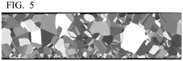
- the insulated circuit substrates (copper/ceramic bonded bodies) obtained in this manner were observed in a cross-sectional surface in the laminating direction and the crystal grain sizes of the circuit layer and metal layer were measured.
- ultrasonic waves were applied thereto and peeling at the bonded interface and cracking of the ceramic substrate were evaluated.
- the average crystal grain size D1 at a position of 50 ⁇ m from the uppermost surface of the ceramic substrate to the circuit layer side and the metal layer side was calculated using the equation below by drawing a reference line parallel to the bonded interface at a position separated by 50 ⁇ m in the laminating direction from the bonded interface of the circuit layer and the metal layer with the ceramic substrate and using the number of particles N touching the reference line and the length L of the reference line.
- the length L of the reference line was as shown in Table 2.
- D 1 1.5 ⁇ L / N
- Terminal materials were ultrasonically welded under conditions of a bonding area of 3 ⁇ 3 mm 2 , a bonding time of approximately 0.6 seconds, and a sinking amount of 0.45 mm and the presence or absence of peeling at the copper/ceramic substrate bonded interface and cracking in the ceramic substrate was confirmed by ultrasonic flaw detection (SAT).
- SAT ultrasonic flaw detection
- the ratio D1/D0 of the average crystal grain size D1 at a position of 50 ⁇ m in the laminating direction from the bonding surface of the circuit layer and the metal layer with the ceramic substrate to the average crystal grain size D0 of the entire circuit layer and metal layer was 0.65 and cracking was generated at the bonded interface when ultrasonic waves were applied thereto.
- Ag-Ti paste was used as the bonding material, the crystal grains in the vicinity of the bonded interface were not sufficiently refined, and it was not possible to suppress deformation in the region in the vicinity of the bonded interface in the circuit layer and metal layer when ultrasonic waves were applied thereto.
- the ratio D1/D0 of the average crystal grain size D1 at a position of 50 ⁇ m in the laminating direction from the bonding surface of the ceramic substrate with the circuit layer and the metal layer to the average crystal grain size D0 of the entire circuit layer and metal layer was 0.60 or less and it was possible to suppress the generation of cracking at the bonded interface when ultrasonic waves were applied thereto.
Landscapes
- Chemical & Material Sciences (AREA)
- Engineering & Computer Science (AREA)
- Ceramic Engineering (AREA)
- Materials Engineering (AREA)
- Structural Engineering (AREA)
- Organic Chemistry (AREA)
- Microelectronics & Electronic Packaging (AREA)
- Inorganic Chemistry (AREA)
- Manufacturing & Machinery (AREA)
- Manufacturing Of Printed Wiring (AREA)
- Cooling Or The Like Of Semiconductors Or Solid State Devices (AREA)
- Ceramic Products (AREA)
Claims (4)
- Kupfer/Keramik-Verbindungskörper, der aus einem Kupferelement, das aus Kupfer oder einer Kupferlegierung gebildet ist, und einem Keramikelement gebildet ist,
wobei ein Verhältnis D1/D0 0,60 oder weniger beträgt, wobei D0 eine durchschnittliche Kristallkorngröße des gesamten Kupferelements ist, wobei Dl eine durchschnittliche Kristallkorngröße des Kupferelements an einer Position ist, die 50 µm von der Verbindungsoberfläche mit dem Keramikelement entfernt ist, wobei D0 und D1 durch Betrachtung des Querschnitts des Kupferelements entlang einer Laminierungsrichtung erhalten werden. - Kupfer/Keramik-Verbindungskörper gemäß Anspruch 1,
wobei Mg in einen Bereich in dem Kupferelement diffundiert ist, wobei der Bereich mindestens 50 µm von der Verbindungsoberfläche mit dem Keramikelement in der Laminierungsrichtung entfernt ist und die Mg-Konzentration mit zunehmender Entfernung von der Verbindungsoberfläche abnimmt. - Isoliertes Schaltungssubstrat, das durch Binden eines Kupferblechs, das aus Kupfer oder einer Kupferlegierung gebildet ist, an eine Oberfläche eines Keramiksubstrats gebildet wird,
wobei ein Verhältnis D1/D0 0,60 oder weniger beträgt, wobei D0 eine durchschnittliche Kristallkorngröße des gesamten Kupferblechs ist, wobei D1 eine durchschnittliche Kristallkorngröße des Kupferblechs an einer Position ist, die 50 µm von der Verbindungsoberfläche mit dem Keramiksubstrat entfernt ist, wobei D0 und D1 durch Betrachtung des Querschnitts des Kupferblechs entlang einer Laminierungsrichtung erhalten werden. - Isoliertes Schaltungssubstrat gemäß Anspruch 3,
wobei Mg in einen Bereich in dem Kupferblech diffundiert ist, wobei der Bereich mindestens 50 µm von der Verbindungsoberfläche mit dem Keramiksubstrat in der Laminierungsrichtung entfernt ist und die Mg-Konzentration mit zunehmender Entfernung von der Verbindungsoberfläche abnimmt.
Applications Claiming Priority (3)
| Application Number | Priority Date | Filing Date | Title |
|---|---|---|---|
| JP2020091953 | 2020-05-27 | ||
| JP2021083912A JP7119268B2 (ja) | 2020-05-27 | 2021-05-18 | 銅/セラミックス接合体、および、絶縁回路基板 |
| PCT/JP2021/019487 WO2021241463A1 (ja) | 2020-05-27 | 2021-05-24 | 銅/セラミックス接合体、および、絶縁回路基板 |
Publications (3)
| Publication Number | Publication Date |
|---|---|
| EP4159704A1 EP4159704A1 (de) | 2023-04-05 |
| EP4159704A4 EP4159704A4 (de) | 2024-07-03 |
| EP4159704B1 true EP4159704B1 (de) | 2025-04-16 |
Family
ID=78744925
Family Applications (1)
| Application Number | Title | Priority Date | Filing Date |
|---|---|---|---|
| EP21813874.1A Active EP4159704B1 (de) | 2020-05-27 | 2021-05-24 | Kupfer/keramik-verbundkörper und isoliertes schaltungssubstrat |
Country Status (6)
| Country | Link |
|---|---|
| US (1) | US20230197556A1 (de) |
| EP (1) | EP4159704B1 (de) |
| KR (1) | KR20230017184A (de) |
| CN (1) | CN115667187A (de) |
| TW (1) | TW202201681A (de) |
| WO (1) | WO2021241463A1 (de) |
Family Cites Families (12)
| Publication number | Priority date | Publication date | Assignee | Title |
|---|---|---|---|---|
| JP3211856B2 (ja) | 1994-11-02 | 2001-09-25 | 電気化学工業株式会社 | 回路基板 |
| JP5129189B2 (ja) * | 2009-03-31 | 2013-01-23 | Dowaメタルテック株式会社 | 金属セラミックス接合基板及びその製造方法 |
| JP2011124585A (ja) * | 2011-01-07 | 2011-06-23 | Hitachi Metals Ltd | セラミックス配線基板、その製造方法及び半導体モジュール |
| JP5991102B2 (ja) * | 2012-09-14 | 2016-09-14 | 三菱マテリアル株式会社 | ヒートシンク付パワーモジュール用基板、ヒートシンク付パワーモジュール、及びヒートシンク付パワーモジュール用基板の製造方法 |
| WO2014148533A1 (ja) * | 2013-03-19 | 2014-09-25 | 日本碍子株式会社 | 接合体及びその製造方法 |
| JP6965768B2 (ja) * | 2017-02-28 | 2021-11-10 | 三菱マテリアル株式会社 | 銅/セラミックス接合体、絶縁回路基板、及び、銅/セラミックス接合体の製造方法、絶縁回路基板の製造方法 |
| WO2018159590A1 (ja) * | 2017-02-28 | 2018-09-07 | 三菱マテリアル株式会社 | 銅/セラミックス接合体、絶縁回路基板、及び、銅/セラミックス接合体の製造方法、絶縁回路基板の製造方法 |
| WO2019082970A1 (ja) * | 2017-10-27 | 2019-05-02 | 三菱マテリアル株式会社 | 接合体、及び、絶縁回路基板 |
| CN111051546B (zh) * | 2018-03-29 | 2021-09-14 | 古河电气工业株式会社 | 绝缘基板及其制造方法 |
| WO2020044593A1 (ja) * | 2018-08-28 | 2020-03-05 | 三菱マテリアル株式会社 | 銅/セラミックス接合体、絶縁回路基板、及び、銅/セラミックス接合体の製造方法、及び、絶縁回路基板の製造方法 |
| JP2020091953A (ja) | 2018-12-03 | 2020-06-11 | シチズン電子株式会社 | 面状発光装置、及び面状発光装置の製造方法 |
| JP7268875B2 (ja) | 2019-11-29 | 2023-05-08 | 株式会社ユニバーサルエンターテインメント | 遊技機 |
-
2021
- 2021-05-24 KR KR1020227039969A patent/KR20230017184A/ko not_active Withdrawn
- 2021-05-24 WO PCT/JP2021/019487 patent/WO2021241463A1/ja not_active Ceased
- 2021-05-24 EP EP21813874.1A patent/EP4159704B1/de active Active
- 2021-05-24 US US17/925,666 patent/US20230197556A1/en active Pending
- 2021-05-24 CN CN202180037561.7A patent/CN115667187A/zh active Pending
- 2021-05-25 TW TW110118789A patent/TW202201681A/zh unknown
Also Published As
| Publication number | Publication date |
|---|---|
| US20230197556A1 (en) | 2023-06-22 |
| EP4159704A1 (de) | 2023-04-05 |
| TW202201681A (zh) | 2022-01-01 |
| CN115667187A (zh) | 2023-01-31 |
| KR20230017184A (ko) | 2023-02-03 |
| WO2021241463A1 (ja) | 2021-12-02 |
| EP4159704A4 (de) | 2024-07-03 |
Similar Documents
| Publication | Publication Date | Title |
|---|---|---|
| EP3590909B1 (de) | Isolierte leiterplatte mit kupfer-keramik-fügekörper, verfahren zur herstellung eines kupfer-keramik-fügekörpers und verfahren zur herstellung einer isolierten leiterplatte | |
| EP3285291B1 (de) | Verbundener körper, substrat für ein leistungsmodul mit einem kühlkörper, kühlkörper, verfahren zur herstellung des verbundenen körpers, verfahren zur herstellung des substrats für ein leistungsmodul mit einem kühlkörper und verfahren zur herstellung eines kühlkörpers | |
| EP2980844B1 (de) | Substrat für leistungsmodule, substrat mit kühlkörper für leistungsmodule und leistungsmodul | |
| JP7056744B2 (ja) | 銅/セラミックス接合体、絶縁回路基板、及び、銅/セラミックス接合体の製造方法、及び、絶縁回路基板の製造方法 | |
| EP3845510A1 (de) | Kupfer-keramik-fügekörper, isolierte leiterplatte und verfahren zur herstellung eines kupfer-keramik-fügekörpers sowie verfahren zur herstellung einer isolierten leiterplatte | |
| US12002732B2 (en) | Copper/ceramic assembly, insulated circuit board, method for producing copper/ceramic assembly, and method for producing insulated circuit board | |
| JP2023523085A (ja) | 金属-セラミック基板を製造する方法及びこのような方法によって製造された金属-セラミック基板 | |
| EP3196930A1 (de) | Anordnung, leistungsmodulsubstrat mit kühlkörper, kühlkörper, verfahren zur herstellung der anordnung, verfahren zur herstellung des leistungsmodulsubstrats mit kühlkörper und verfahren zur herstellung eines kühlkörpers | |
| EP4071128B1 (de) | Kupfer-keramik-fügekörper, isolierende leiterplatte, verfahren zur herstellung eines kupfer-keramik-fügekörpers sowie verfahren zur herstellung einer isolierenden leiterplatte | |
| EP3578535A1 (de) | Keramik-/aluminiumkonjugat, isolierte leiterplatte, led-modul, keramikteil, verfahren zur herstellung von keramik-/aluminium-konjugat und verfahren zur herstellung von isolierten leiterplatten | |
| JP7119268B2 (ja) | 銅/セラミックス接合体、および、絶縁回路基板 | |
| US12125765B2 (en) | Copper/ceramic joined body and insulating circuit substrate | |
| EP3845511B1 (de) | Kupfer-keramik-fügekörper, isolierte leiterplatte, verfahren zur herstellung eines kupfer-keramik-fügekörpers sowie verfahren zur herstellung einer isolierten leiterplatte | |
| EP4053091A1 (de) | Kupfer-/keramikanordnung, isolierte leiterplatte, verfahren zur herstellung einer kupfer-/keramikanordnung und verfahren zur herstellung einer isolierten leiterplatte | |
| EP3960722B1 (de) | Kupfer-keramikverbundkörper, isolierschaltungssubstrat, verfahren zur herstellung eines kupfer-keramikverbundkörpers und verfahren zur herstellung eines isolierschaltungssubstrats | |
| EP4159704B1 (de) | Kupfer/keramik-verbundkörper und isoliertes schaltungssubstrat | |
| EP4585581A1 (de) | Kupfer/keramik verbundkörper und isolierte leiterplatte | |
| EP4074678B1 (de) | Kupfer-/keramikanordnung und isolierte leiterplatte | |
| EP3703116B1 (de) | Verbundener körper, isolierte platine mit kühlkörper und kühlkörper | |
| EP4071127A1 (de) | Kupfer-/keramikanordnung, isolierte leiterplatte, verfahren zur herstellung einer kupfer-/keramikanordnung und verfahren zur herstellung einer isolierten leiterplatte | |
| JPWO2006098233A1 (ja) | 電子部品用パッケージ、その蓋体、その蓋体用の蓋材及びその蓋材の製造方法 | |
| JP2021031315A (ja) | 銅/セラミックス接合体、絶縁回路基板、及び、銅/セラミックス接合体の製造方法、絶縁回路基板の製造方法 | |
| EP4328208A1 (de) | Kupfer/keramik verbundkörper und isolierte leiterplatte | |
| EP4378914A1 (de) | Kupfer/keramik verbundkörper und isolierte leiterplatte | |
| EP3754701B1 (de) | Kupfer/titan/aluminium-verbindung, isolierende leiterplatte, isolierende leiterplatte mit kühlkörper, leistungsmodul, led-modul und thermoelektrisches modul |
Legal Events
| Date | Code | Title | Description |
|---|---|---|---|
| STAA | Information on the status of an ep patent application or granted ep patent |
Free format text: STATUS: THE INTERNATIONAL PUBLICATION HAS BEEN MADE |
|
| PUAI | Public reference made under article 153(3) epc to a published international application that has entered the european phase |
Free format text: ORIGINAL CODE: 0009012 |
|
| STAA | Information on the status of an ep patent application or granted ep patent |
Free format text: STATUS: REQUEST FOR EXAMINATION WAS MADE |
|
| 17P | Request for examination filed |
Effective date: 20221117 |
|
| AK | Designated contracting states |
Kind code of ref document: A1 Designated state(s): AL AT BE BG CH CY CZ DE DK EE ES FI FR GB GR HR HU IE IS IT LI LT LU LV MC MK MT NL NO PL PT RO RS SE SI SK SM TR |
|
| DAV | Request for validation of the european patent (deleted) | ||
| DAX | Request for extension of the european patent (deleted) | ||
| A4 | Supplementary search report drawn up and despatched |
Effective date: 20240605 |
|
| RIC1 | Information provided on ipc code assigned before grant |
Ipc: C04B 35/645 20060101ALI20240529BHEP Ipc: H05K 1/02 20060101ALI20240529BHEP Ipc: C04B 37/02 20060101AFI20240529BHEP |
|
| GRAP | Despatch of communication of intention to grant a patent |
Free format text: ORIGINAL CODE: EPIDOSNIGR1 |
|
| STAA | Information on the status of an ep patent application or granted ep patent |
Free format text: STATUS: GRANT OF PATENT IS INTENDED |
|
| INTG | Intention to grant announced |
Effective date: 20241213 |
|
| GRAS | Grant fee paid |
Free format text: ORIGINAL CODE: EPIDOSNIGR3 |
|
| GRAA | (expected) grant |
Free format text: ORIGINAL CODE: 0009210 |
|
| STAA | Information on the status of an ep patent application or granted ep patent |
Free format text: STATUS: THE PATENT HAS BEEN GRANTED |
|
| AK | Designated contracting states |
Kind code of ref document: B1 Designated state(s): AL AT BE BG CH CY CZ DE DK EE ES FI FR GB GR HR HU IE IS IT LI LT LU LV MC MK MT NL NO PL PT RO RS SE SI SK SM TR |
|
| REG | Reference to a national code |
Ref country code: GB Ref legal event code: FG4D |
|
| REG | Reference to a national code |
Ref country code: CH Ref legal event code: EP |
|
| REG | Reference to a national code |
Ref country code: IE Ref legal event code: FG4D |
|
| REG | Reference to a national code |
Ref country code: DE Ref legal event code: R096 Ref document number: 602021029331 Country of ref document: DE |
|
| PGFP | Annual fee paid to national office [announced via postgrant information from national office to epo] |
Ref country code: DE Payment date: 20250520 Year of fee payment: 5 |
|
| PGFP | Annual fee paid to national office [announced via postgrant information from national office to epo] |
Ref country code: AT Payment date: 20250721 Year of fee payment: 5 |
|
| REG | Reference to a national code |
Ref country code: NL Ref legal event code: MP Effective date: 20250416 |
|
| PG25 | Lapsed in a contracting state [announced via postgrant information from national office to epo] |
Ref country code: NL Free format text: LAPSE BECAUSE OF FAILURE TO SUBMIT A TRANSLATION OF THE DESCRIPTION OR TO PAY THE FEE WITHIN THE PRESCRIBED TIME-LIMIT Effective date: 20250416 |
|
| REG | Reference to a national code |
Ref country code: AT Ref legal event code: MK05 Ref document number: 1785590 Country of ref document: AT Kind code of ref document: T Effective date: 20250416 |
|
| PG25 | Lapsed in a contracting state [announced via postgrant information from national office to epo] |
Ref country code: FI Free format text: LAPSE BECAUSE OF FAILURE TO SUBMIT A TRANSLATION OF THE DESCRIPTION OR TO PAY THE FEE WITHIN THE PRESCRIBED TIME-LIMIT Effective date: 20250416 Ref country code: PT Free format text: LAPSE BECAUSE OF FAILURE TO SUBMIT A TRANSLATION OF THE DESCRIPTION OR TO PAY THE FEE WITHIN THE PRESCRIBED TIME-LIMIT Effective date: 20250818 Ref country code: ES Free format text: LAPSE BECAUSE OF FAILURE TO SUBMIT A TRANSLATION OF THE DESCRIPTION OR TO PAY THE FEE WITHIN THE PRESCRIBED TIME-LIMIT Effective date: 20250416 |
|
| REG | Reference to a national code |
Ref country code: LT Ref legal event code: MG9D |
|
| PG25 | Lapsed in a contracting state [announced via postgrant information from national office to epo] |
Ref country code: NO Free format text: LAPSE BECAUSE OF FAILURE TO SUBMIT A TRANSLATION OF THE DESCRIPTION OR TO PAY THE FEE WITHIN THE PRESCRIBED TIME-LIMIT Effective date: 20250716 Ref country code: GR Free format text: LAPSE BECAUSE OF FAILURE TO SUBMIT A TRANSLATION OF THE DESCRIPTION OR TO PAY THE FEE WITHIN THE PRESCRIBED TIME-LIMIT Effective date: 20250717 |
|
| PG25 | Lapsed in a contracting state [announced via postgrant information from national office to epo] |
Ref country code: PL Free format text: LAPSE BECAUSE OF FAILURE TO SUBMIT A TRANSLATION OF THE DESCRIPTION OR TO PAY THE FEE WITHIN THE PRESCRIBED TIME-LIMIT Effective date: 20250416 |
|
| PG25 | Lapsed in a contracting state [announced via postgrant information from national office to epo] |
Ref country code: BG Free format text: LAPSE BECAUSE OF FAILURE TO SUBMIT A TRANSLATION OF THE DESCRIPTION OR TO PAY THE FEE WITHIN THE PRESCRIBED TIME-LIMIT Effective date: 20250416 |
|
| PG25 | Lapsed in a contracting state [announced via postgrant information from national office to epo] |
Ref country code: HR Free format text: LAPSE BECAUSE OF FAILURE TO SUBMIT A TRANSLATION OF THE DESCRIPTION OR TO PAY THE FEE WITHIN THE PRESCRIBED TIME-LIMIT Effective date: 20250416 |
|
| PG25 | Lapsed in a contracting state [announced via postgrant information from national office to epo] |
Ref country code: AT Free format text: LAPSE BECAUSE OF FAILURE TO SUBMIT A TRANSLATION OF THE DESCRIPTION OR TO PAY THE FEE WITHIN THE PRESCRIBED TIME-LIMIT Effective date: 20250416 |
|
| PG25 | Lapsed in a contracting state [announced via postgrant information from national office to epo] |
Ref country code: RS Free format text: LAPSE BECAUSE OF FAILURE TO SUBMIT A TRANSLATION OF THE DESCRIPTION OR TO PAY THE FEE WITHIN THE PRESCRIBED TIME-LIMIT Effective date: 20250716 |
|
| PG25 | Lapsed in a contracting state [announced via postgrant information from national office to epo] |
Ref country code: IS Free format text: LAPSE BECAUSE OF FAILURE TO SUBMIT A TRANSLATION OF THE DESCRIPTION OR TO PAY THE FEE WITHIN THE PRESCRIBED TIME-LIMIT Effective date: 20250816 |
|
| PG25 | Lapsed in a contracting state [announced via postgrant information from national office to epo] |
Ref country code: LV Free format text: LAPSE BECAUSE OF FAILURE TO SUBMIT A TRANSLATION OF THE DESCRIPTION OR TO PAY THE FEE WITHIN THE PRESCRIBED TIME-LIMIT Effective date: 20250416 |
|
| REG | Reference to a national code |
Ref country code: CH Ref legal event code: H13 Free format text: ST27 STATUS EVENT CODE: U-0-0-H10-H13 (AS PROVIDED BY THE NATIONAL OFFICE) Effective date: 20251223 |
|
| PG25 | Lapsed in a contracting state [announced via postgrant information from national office to epo] |
Ref country code: SM Free format text: LAPSE BECAUSE OF FAILURE TO SUBMIT A TRANSLATION OF THE DESCRIPTION OR TO PAY THE FEE WITHIN THE PRESCRIBED TIME-LIMIT Effective date: 20250416 Ref country code: DK Free format text: LAPSE BECAUSE OF FAILURE TO SUBMIT A TRANSLATION OF THE DESCRIPTION OR TO PAY THE FEE WITHIN THE PRESCRIBED TIME-LIMIT Effective date: 20250416 |
|
| PG25 | Lapsed in a contracting state [announced via postgrant information from national office to epo] |
Ref country code: LU Free format text: LAPSE BECAUSE OF NON-PAYMENT OF DUE FEES Effective date: 20250524 |
|
| PG25 | Lapsed in a contracting state [announced via postgrant information from national office to epo] |
Ref country code: CH Free format text: LAPSE BECAUSE OF NON-PAYMENT OF DUE FEES Effective date: 20250531 |
|
| REG | Reference to a national code |
Ref country code: DE Ref legal event code: R097 Ref document number: 602021029331 Country of ref document: DE |
|
| PG25 | Lapsed in a contracting state [announced via postgrant information from national office to epo] |
Ref country code: CZ Free format text: LAPSE BECAUSE OF FAILURE TO SUBMIT A TRANSLATION OF THE DESCRIPTION OR TO PAY THE FEE WITHIN THE PRESCRIBED TIME-LIMIT Effective date: 20250416 |
|
| PG25 | Lapsed in a contracting state [announced via postgrant information from national office to epo] |
Ref country code: EE Free format text: LAPSE BECAUSE OF FAILURE TO SUBMIT A TRANSLATION OF THE DESCRIPTION OR TO PAY THE FEE WITHIN THE PRESCRIBED TIME-LIMIT Effective date: 20250416 |
|
| PG25 | Lapsed in a contracting state [announced via postgrant information from national office to epo] |
Ref country code: SK Free format text: LAPSE BECAUSE OF FAILURE TO SUBMIT A TRANSLATION OF THE DESCRIPTION OR TO PAY THE FEE WITHIN THE PRESCRIBED TIME-LIMIT Effective date: 20250416 |
|
| PG25 | Lapsed in a contracting state [announced via postgrant information from national office to epo] |
Ref country code: IT Free format text: LAPSE BECAUSE OF FAILURE TO SUBMIT A TRANSLATION OF THE DESCRIPTION OR TO PAY THE FEE WITHIN THE PRESCRIBED TIME-LIMIT Effective date: 20250416 |
|
| REG | Reference to a national code |
Ref country code: BE Ref legal event code: MM Effective date: 20250531 |
|
| PG25 | Lapsed in a contracting state [announced via postgrant information from national office to epo] |
Ref country code: MC Free format text: LAPSE BECAUSE OF FAILURE TO SUBMIT A TRANSLATION OF THE DESCRIPTION OR TO PAY THE FEE WITHIN THE PRESCRIBED TIME-LIMIT Effective date: 20250416 |
|
| PG25 | Lapsed in a contracting state [announced via postgrant information from national office to epo] |
Ref country code: RO Free format text: LAPSE BECAUSE OF FAILURE TO SUBMIT A TRANSLATION OF THE DESCRIPTION OR TO PAY THE FEE WITHIN THE PRESCRIBED TIME-LIMIT Effective date: 20250416 |
|
| PLBE | No opposition filed within time limit |
Free format text: ORIGINAL CODE: 0009261 |
|
| STAA | Information on the status of an ep patent application or granted ep patent |
Free format text: STATUS: NO OPPOSITION FILED WITHIN TIME LIMIT |
|
| REG | Reference to a national code |
Ref country code: CH Ref legal event code: L10 Free format text: ST27 STATUS EVENT CODE: U-0-0-L10-L00 (AS PROVIDED BY THE NATIONAL OFFICE) Effective date: 20260225 |
|
| 26N | No opposition filed |
Effective date: 20260119 |
|
| GBPC | Gb: european patent ceased through non-payment of renewal fee |
Effective date: 20250716 |
|
| PG25 | Lapsed in a contracting state [announced via postgrant information from national office to epo] |
Ref country code: GB Free format text: LAPSE BECAUSE OF NON-PAYMENT OF DUE FEES Effective date: 20250716 |
|
| PG25 | Lapsed in a contracting state [announced via postgrant information from national office to epo] |
Ref country code: IE Free format text: LAPSE BECAUSE OF NON-PAYMENT OF DUE FEES Effective date: 20250524 |
|
| PG25 | Lapsed in a contracting state [announced via postgrant information from national office to epo] |
Ref country code: BE Free format text: LAPSE BECAUSE OF NON-PAYMENT OF DUE FEES Effective date: 20250531 |
|
| PG25 | Lapsed in a contracting state [announced via postgrant information from national office to epo] |
Ref country code: FR Free format text: LAPSE BECAUSE OF NON-PAYMENT OF DUE FEES Effective date: 20250616 |