EP4156418A2 - Fester verbinder und verbinderanordnung damit - Google Patents
Fester verbinder und verbinderanordnung damit Download PDFInfo
- Publication number
- EP4156418A2 EP4156418A2 EP22197307.6A EP22197307A EP4156418A2 EP 4156418 A2 EP4156418 A2 EP 4156418A2 EP 22197307 A EP22197307 A EP 22197307A EP 4156418 A2 EP4156418 A2 EP 4156418A2
- Authority
- EP
- European Patent Office
- Prior art keywords
- signal pin
- substrate
- dielectric
- fixed connector
- disposed
- Prior art date
- Legal status (The legal status is an assumption and is not a legal conclusion. Google has not performed a legal analysis and makes no representation as to the accuracy of the status listed.)
- Granted
Links
Images


Classifications
-
- H—ELECTRICITY
- H01—ELECTRIC ELEMENTS
- H01R—ELECTRICALLY-CONDUCTIVE CONNECTIONS; STRUCTURAL ASSOCIATIONS OF A PLURALITY OF MUTUALLY-INSULATED ELECTRICAL CONNECTING ELEMENTS; COUPLING DEVICES; CURRENT COLLECTORS
- H01R24/00—Two-part coupling devices, or either of their cooperating parts, characterised by their overall structure
- H01R24/38—Two-part coupling devices, or either of their cooperating parts, characterised by their overall structure having concentrically or coaxially arranged contacts
- H01R24/40—Two-part coupling devices, or either of their cooperating parts, characterised by their overall structure having concentrically or coaxially arranged contacts specially adapted for high frequency
- H01R24/50—Two-part coupling devices, or either of their cooperating parts, characterised by their overall structure having concentrically or coaxially arranged contacts specially adapted for high frequency mounted on a PCB [Printed Circuit Board]
-
- H—ELECTRICITY
- H01—ELECTRIC ELEMENTS
- H01R—ELECTRICALLY-CONDUCTIVE CONNECTIONS; STRUCTURAL ASSOCIATIONS OF A PLURALITY OF MUTUALLY-INSULATED ELECTRICAL CONNECTING ELEMENTS; COUPLING DEVICES; CURRENT COLLECTORS
- H01R12/00—Structural associations of a plurality of mutually-insulated electrical connecting elements, specially adapted for printed circuits, e.g. printed circuit boards [PCB], flat or ribbon cables, or like generally planar structures, e.g. terminal strips, terminal blocks; Coupling devices specially adapted for printed circuits, flat or ribbon cables, or like generally planar structures; Terminals specially adapted for contact with, or insertion into, printed circuits, flat or ribbon cables, or like generally planar structures
- H01R12/50—Fixed connections
- H01R12/51—Fixed connections for rigid printed circuits or like structures
- H01R12/55—Fixed connections for rigid printed circuits or like structures characterised by the terminals
- H01R12/58—Fixed connections for rigid printed circuits or like structures characterised by the terminals terminals for insertion into holes
-
- H—ELECTRICITY
- H01—ELECTRIC ELEMENTS
- H01R—ELECTRICALLY-CONDUCTIVE CONNECTIONS; STRUCTURAL ASSOCIATIONS OF A PLURALITY OF MUTUALLY-INSULATED ELECTRICAL CONNECTING ELEMENTS; COUPLING DEVICES; CURRENT COLLECTORS
- H01R12/00—Structural associations of a plurality of mutually-insulated electrical connecting elements, specially adapted for printed circuits, e.g. printed circuit boards [PCB], flat or ribbon cables, or like generally planar structures, e.g. terminal strips, terminal blocks; Coupling devices specially adapted for printed circuits, flat or ribbon cables, or like generally planar structures; Terminals specially adapted for contact with, or insertion into, printed circuits, flat or ribbon cables, or like generally planar structures
- H01R12/70—Coupling devices
- H01R12/7005—Guiding, mounting, polarizing or locking means; Extractors
- H01R12/7011—Locking or fixing a connector to a PCB
- H01R12/7052—Locking or fixing a connector to a PCB characterised by the locating members
-
- H—ELECTRICITY
- H01—ELECTRIC ELEMENTS
- H01R—ELECTRICALLY-CONDUCTIVE CONNECTIONS; STRUCTURAL ASSOCIATIONS OF A PLURALITY OF MUTUALLY-INSULATED ELECTRICAL CONNECTING ELEMENTS; COUPLING DEVICES; CURRENT COLLECTORS
- H01R12/00—Structural associations of a plurality of mutually-insulated electrical connecting elements, specially adapted for printed circuits, e.g. printed circuit boards [PCB], flat or ribbon cables, or like generally planar structures, e.g. terminal strips, terminal blocks; Coupling devices specially adapted for printed circuits, flat or ribbon cables, or like generally planar structures; Terminals specially adapted for contact with, or insertion into, printed circuits, flat or ribbon cables, or like generally planar structures
- H01R12/70—Coupling devices
- H01R12/7005—Guiding, mounting, polarizing or locking means; Extractors
- H01R12/7011—Locking or fixing a connector to a PCB
- H01R12/707—Soldering or welding
-
- H—ELECTRICITY
- H01—ELECTRIC ELEMENTS
- H01R—ELECTRICALLY-CONDUCTIVE CONNECTIONS; STRUCTURAL ASSOCIATIONS OF A PLURALITY OF MUTUALLY-INSULATED ELECTRICAL CONNECTING ELEMENTS; COUPLING DEVICES; CURRENT COLLECTORS
- H01R12/00—Structural associations of a plurality of mutually-insulated electrical connecting elements, specially adapted for printed circuits, e.g. printed circuit boards [PCB], flat or ribbon cables, or like generally planar structures, e.g. terminal strips, terminal blocks; Coupling devices specially adapted for printed circuits, flat or ribbon cables, or like generally planar structures; Terminals specially adapted for contact with, or insertion into, printed circuits, flat or ribbon cables, or like generally planar structures
- H01R12/70—Coupling devices
- H01R12/7082—Coupling device supported only by cooperation with PCB
-
- H—ELECTRICITY
- H01—ELECTRIC ELEMENTS
- H01R—ELECTRICALLY-CONDUCTIVE CONNECTIONS; STRUCTURAL ASSOCIATIONS OF A PLURALITY OF MUTUALLY-INSULATED ELECTRICAL CONNECTING ELEMENTS; COUPLING DEVICES; CURRENT COLLECTORS
- H01R12/00—Structural associations of a plurality of mutually-insulated electrical connecting elements, specially adapted for printed circuits, e.g. printed circuit boards [PCB], flat or ribbon cables, or like generally planar structures, e.g. terminal strips, terminal blocks; Coupling devices specially adapted for printed circuits, flat or ribbon cables, or like generally planar structures; Terminals specially adapted for contact with, or insertion into, printed circuits, flat or ribbon cables, or like generally planar structures
- H01R12/70—Coupling devices
- H01R12/91—Coupling devices allowing relative movement between coupling parts, e.g. floating or self aligning
-
- H—ELECTRICITY
- H01—ELECTRIC ELEMENTS
- H01R—ELECTRICALLY-CONDUCTIVE CONNECTIONS; STRUCTURAL ASSOCIATIONS OF A PLURALITY OF MUTUALLY-INSULATED ELECTRICAL CONNECTING ELEMENTS; COUPLING DEVICES; CURRENT COLLECTORS
- H01R2103/00—Two poles
Definitions
- the present invention relates to a fixed connector and a connector assembly including the same.
- radio frequency (RF) connectors are used in various forms on a substrate (printed circuit board (PCB)) of wired/wireless communication devices (for example, mobile communication repeaters).
- a substrate printed circuit board (PCB)
- wired/wireless communication devices for example, mobile communication repeaters
- One side of the RF connector may be soldered and fixed to a substrate, and the other side thereof may be coupled to a device (for example, a connector).
- SMT surface mount technology
- PCB thru hole (PTH) method in which a signal pin and a lead of an RF connector passes through a substrate (PCB) has been used, since the PTH method requires an additional wave soldering process, a pin-in-paste (PIP) waveless soldering method that supplements this is being used.
- PTH PCB thru hole
- PIP pin-in-paste
- the present invention is directed to providing a fixed connector having a novel structure capable of maximizing a fixing force (soldering strength) between a connector and a substrate while maintaining ease of manufacturing, and a connector assembly including the same.
- One aspect of the present invention provides a fixed connector including a body fixedly inserted into a substrate, a signal pin having one side inserted into the body and the other side extending from the one side to be disposed on the substrate, and a dielectric coupling the signal pin and the body, wherein a portion of the signal pin has an L shape to be in contact with the substrate, and the portion of the signal pin is exposed to an outside of the body.
- the signal pin may include a first signal pin inserted into the body, and a second signal pin disposed on the substrate and electrically connected to the first signal pin.
- an end portion of the first signal pin may be coupled to the second signal pin through a hole formed in the second signal pin.
- the body may include a body part surrounding a first signal pin, which is inserted into the body, among the signal pin, and a plurality of leads integrally formed with the body part, connected to a lower portion of the body part, and inserted into the substrate.
- the body part may have a vertical cross section that is symmetrical in a left-right direction with respect to a central axis in a direction in which a second signal pin, which is disposed on the substrate, among the signal pin is oriented.
- the plurality of leads may be each formed in a rod shape at an edge of a bottom surface of the body part and are asymmetric in the left-right direction.
- a cross section of one or more of the plurality of leads may be different from a cross section of the remaining leads.
- one region of a second signal pin disposed on the substrate may have an arcuate shape.
- the dielectric may be disposed to surround a lower end of the signal pin, and a cross section of a protruding region of the dielectric may be identical or similar to a cross section of an inner space of the body so that the dielectric is fixedly fitted into the inner space of the body.
- the dielectric may include a first dielectric surrounding the first signal pin, and a second dielectric surrounding the second signal pin, and a shape of a bottom surface of the second dielectric coupling the second signal pin may correspond to a shape of a groove formed in the body part.
- the body may have a groove for coupling with the dielectric.
- the dielectric may have a press-fitting protrusion for coupling with the body in a direction toward an upper end of the body.
- the groove and the press-fitting protrusion may be arranged at a location corresponding to a second signal pin, which is disposed on the substrate, among the signal pin.
- One region of the dielectric for coupling a second signal pin, among the signal pin, disposed on the substrate to the body may have at least a partial shape of a circle.
- At least one circular groove may be formed in a bottom surface corresponding to the substrate or an annular groove may be formed to be open in a direction in which the second signal pin disposed on the substrate is oriented on the basis of a center of a first signal pin, which is inserted into the body, among the signal pin.
- the body may include a second groove through which the second signal pin, which is disposed on the substrate, among the signal pin passes, and a first groove formed in one side of a bottom surface of the body facing the second groove formed in the other side of the bottom surface of the body.
- the body may have an air gap between the body and the dielectric disposed on a second signal pin, which is disposed on the substrate, among the signal pin.
- the body part may have a plurality of grooves between the plurality of leads, and among the plurality of grooves, grooves through which the second signal pin passes may have a greater width or height than that of the remaining grooves.
- the signal pin includes: a first signal pin inserted into the body; and a second signal pin disposed on the substrate and electrically connected to the first signal pin, and in the first signal pin and the second signal pin, an end portion of the first signal pin is coupled to the second signal pin through a hole formed in the second signal pin.
- the signal pin, one region of a second signal pin disposed on the substrate has an arcuate shape.
- the dielectric is disposed to surround a lower end of the signal pin, and a cross section of a protruding region of the dielectric is identical or similar to a cross section of an inner space of the body so that the dielectric is fixedly fitted into the inner space of the body.
- the body has an air gap between the body and the dielectric disposed on a second signal pin, which is disposed on the substrate, among the signal pin.
- a signal pin to be electrically connected to a substrate is configured in an L shape, a fixing force between the substrate and a connector is increased, a longer length of a signal pin is secured, and thus frequency characteristics can be maintained.
- FIG. 1 is a view for describing a structure of a connector assembly according to a related art.
- a conventional connector assembly 1 includes a conventional fixed connector 2 and a conventional connection connector 4 fixed to a substrate 10, and in the conventional fixed connector 2, a signal pin A1 and a lead A2 to be fixed to the substrate 10 in a pin-in-paste (PIP) manner may be inserted into the substrate 10.
- PIP pin-in-paste
- the conventional connector assembly 1 may secure an improved fixing force with the substrate 10 as compared to a surface mount technology (SMT) method, but the length of the signal pin A1 of the conventional fixed connector 2 is set to a length at which the signal pin A1 does not pass through the substrate 10, and thus the characteristics of a specific frequency are degraded.
- SMT surface mount technology
- FIG. 2 is an exploded perspective view of a connector assembly according to an embodiment of the present invention.
- a connector assembly 1000 may include a fixed connector 20 and a connection connector 40.
- the fixed connector 20 may be fixed to the substrate 10
- the connection connector 40 may be coupled to a device (for example, a connector), and thus an electrical signal may be supplied between the fixed connector 20 and the device (for example, a connector).
- the connection connector 40 may be coupled to the device in a female/male connector structure.
- the fixed connector 20 may include a solderable body 100, a signal pin 200 including a first signal pin 210 and a second signal pin 220 through which an electrical signal is transmitted, and a dielectric 300 that insulates the signal pin 200 and the body 100 from each other.
- the second signal pin 220 may include a coupling hole 225 to be fixed to one end of the first signal pin 210, and the signal pin 200 may be formed in an L shape in which the second signal pin 220 is bent in first and second directions from the first signal pin 210 through the coupling hole 225.
- first and second signal pins 210 and 220 may be coupled in various ways through the coupling hole 225.
- the first signal pin 210 may be pressfitted into the coupling hole 225 to be coupled, the first signal pin 210 may protrude and be inserted into the coupling hole 225 and then coupled to the coupling hole 225 in a rivet manner, and the first signal pin 210 may be also coupled to the coupling hole 225 through screw grooves formed outside one end of the first signal pin 210 and inside the coupling hole 225 of the second signal pin 220.
- the second signal pin 220 may be disposed such that a portion thereof is exposed to the outside of the body 100 and may be electrically connected to a signal electrode SE formed on the substrate 10 in a partial region thereof exposed to the outside by soldering.
- first and second signal pins 210 and 220 of the fixed connector 20 are separated, the first and second signal pins 210 and 220 may be integrally formed.
- the connection connector 40 may include a connection body 410, first and second connection conductors 420 and 430, and a connection dielectric 440.
- the first and second connection conductors 420 and 430 may be inserted into the connection body 410 and may be insulated from the connection body 410.
- the connection dielectric 440 may be inserted into the connection body 410, and may insulate the first and second signal pins 210 and 220 and the first and second connection conductors 420 and 430 from each other.
- connection body 410 may be coupled to the body 100 of the fixed connector 20, and thus the first and second signal pins 210 and 220 of the fixed connector 20 may be electrically connected to the first and second connection conductors 420 and 430.
- both ends of the first and second connection conductors 420 and 430 include connection grooves (not illustrated), and one end of the first signal pin 210 may be inserted into and coupled to the connection grooves located at ends of the first and second connection conductors 420 and 430.
- a signal pin of the device may be inserted into and coupled to the connection grooves formed at the other ends of the first and second connection conductors 420 and 430.
- first and second connection conductors 420 and 430 of the connection connector 40 are separated, the first and second connection conductors 420 and 430 may be integrally formed.
- a coupling portion 215 may be formed at one end of the first signal pin 210 coupled to and inserted into the first and second connection conductors 420 and 430 so that the first signal pin 210 is inserted and then maintains a contact state.
- the coupling portion 215 of the first signal pin 210 is formed as a slit so that the size of the diameter may be adjusted, and thus inserted into the connection grooves, and the contact state may be maintained by the coupling portion 215.
- FIG. 3 is a cross-sectional view of a fixed connector according to an embodiment of the present invention.
- the fixed connector 20 may include the body 100, the first signal pin 210, the second signal pin 220, and the dielectric 300.
- the body 100 may be inserted into and fixed to the substrate 10 through a soldering method and may include a body part 110 that is a region coupled to the connection connector 40 and a plurality of leads 120 that are regions inserted and soldered into the substrate 10. In this way, as the leads 120 of the body 100 are coupled to the substrate 10 in a PIP manner, the fixing force with the substrate 10 can be improved as compared to an SMD method.
- the body 100 may have a hollow shape so that the first signal pin 210 may be inserted thereinto and may be insulated from the first signal pin 210.
- the first signal pin 210 may be inserted into the body 100.
- the first signal pin 210 is insulated from the body 100 but may be electrically connected to the first and second connection conductors 420 and 430 at one end thereof and electrically connected to the second signal pin 220 at the other end thereof.
- the second signal pin 220 may be disposed on the substrate 10 and may be electrically connected to the first signal pin 210 through the coupling hole 225 formed at one end thereof.
- the two signal pins 210 and 220 may be electrically connected.
- the second signal pin 220 may not be inserted into the substrate 10, may be disposed in parallel on the substrate 10, and may be electrically connected to the signal electrode SE formed on the substrate 10 through soldering.
- a portion of the second signal pin 220 exposed to the outside of the body 100 may be electrically connected to the signal electrode SE formed on the substrate 10 through soldering.
- the second signal pin 220 disposed on the substrate 10 may be disposed on the substrate 10 to be longer than the thickness of the substrate 10, and by securing the length of the signal pin 200 in an L shape, RF loss occurring at a high frequency of, for example, 3 GHz or more can be reduced while increasing a fixing force between the substrate 10 and the fixed connector 20. Further, since the portion of the second signal pin 220 exposed to the outside of the body 100 is soldered to the signal electrode SE formed on the substrate 10, the occurrence of a cold solder joint can be prevented.
- the signal pin 200 of the fixed connector 20 is not separated into two parts and may be formed in an integral form in which one side thereof may be inserted into the body 100 and the other side thereof extending from the one side is disposed to extend on the substrate 10. Accordingly, the signal pin 200 may be bent at a portion in contact with the substrate 10 to form an L shape.
- the dielectric 300 may couple the signal pin 200 and the body 100.
- the first and second signal pins 210 and 220 are arranged inside the hollow inner space of the body 100, and thus the body 100 may be physically coupled to the first and second signal pins 210 and 220 while insulated from the first and second signal pins 210 and 220.
- FIG. 4A and FIG. 4B is an enlarged cross-sectional view illustrating only a partial configuration of the fixed connector according to an embodiment of the present invention.
- the signal pin 200 may be divided into the first and second signal pins 210 and 220 or may be integrally formed, and the dielectric 300 may couple the signal pin 200 having an L shape to the inside of the body 100.
- the dielectric 300 may be injection-molded with the signal pin 200. As the dielectric 300 is injection-molded, the dielectric 300 may fill an empty space B formed in an arcuate shape of the second signal pin 220, and a fixing force between the dielectric 300 and the signal pin 200 can be more increased as compared to a case in which the second signal pin 220 has a flat structure.
- the dielectric 300 may be formed of various synthetic resin-based materials and may be formed of a heat-resistant material, thereby reducing deformation due to heat of soldering.
- the dielectric 300 may be formed of a material such as a liquid crystal polymer (LCP), polyphenylene sulfide (PPS), polyphenylene oxide (PPO), polyetheretherketone (PEEK), and polyether imide (ULTEM).
- LCP liquid crystal polymer
- PPS polyphenylene sulfide
- PPO polyphenylene oxide
- PEEK polyetheretherketone
- ULTEM polyether imide
- the dielectric 300 may have a separate structure to couple each of the first and second signal pins 220 to the body 100, and a detailed description thereof will be made below.
- FIG. 5A and FIG. 5B is a view for describing a body of the fixed connector according to an embodiment of the present invention.
- the body 100 of the fixed connector 20 may include the body part 110 and the plurality of leads 120.
- the body 100 may be made of a metal material and may be electrically insulated from the first and second signal pins 210 and 220 by the dielectric 300.
- the body part 110 may surround the first signal pin 210, which is inserted into the body 100, among the signal pin 200.
- a vertical cross section of the body part 110 with respect to the first signal pin 210 as a central axis may be symmetrical in a left-right direction based on a direction in which the second signal pin 220 is oriented.
- the body part 110 is symmetrical in the left-right direction, and thus the fixed connector 20 may be more easily picked up and seated on the substrate 10.
- the plurality of leads 120 may be connected to a lower portion of the body part 110 of the body 100 and inserted into the substrate 10.
- the body part 110 and the plurality of leads 120 may be integrally formed, and may be inserted into and soldered to the substrate 10 in an integrally formed state, and thus the fixed connector 20 may be stably fixed to the substrate 10.
- first grooves H1 may be formed between a first lead 120a and a second lead 120b, between the first lead 120a and a third lead 120c, and between the third lead 120c and a fourth lead 120d, and a second groove H2 may be formed between the second lead 120b and the fourth lead 120d.
- the second groove H2 through which the second signal pin 220 passes may be formed to have a greater width or height than the remaining first groove H1, and through these empty spaces, even when the signal pin 200 is formed in an L shape, return loss and insertion loss values of the fixed connector 20 can be maintained.
- the first and second grooves H1 and H2 may separate a bottom surface of the body part 110 based on each of the plurality of leads 120.
- the bottom surface of the separated body part 110 is seated on and soldered to a ground electrode GE of the substrate 10 formed separately based on each of grooves into which the plurality of leads 120 are inserted, and thereby alignment between the fixed connector 20 and the substrate 10 can be improved utilizing the surface tension of the soldering.
- the plurality of leads 120 may be formed in a bar shape at an edge of the bottom surface of the body part 110 and may be asymmetrical in the left-right direction.
- the signal pin 200 of the fixed connector 20 has an L shape, when the existing process is used without change, a situation may occur in which the second signal pin 220 of the fixed connector 20 is not properly seated on the signal electrode SE formed on the substrate 10.
- the fixed connector 20 may provide a difference in the shape of the plurality of leads 120.
- the cross section of one or more of the leads 120 may be different from the cross section of the other leads 120.
- a horizontal cross-sectional shape of the first lead 120a among the plurality of leads 120 may be circular, and a horizontal cross-sectional shape of the remaining second, third, and fourth leads 120b, 120c, and 120d may be quadrangular.
- the thickness of the first and third leads 120a and 120c may be greater or smaller than the thickness of the second and third leads 120b and 120d.
- the body part 110 has the symmetrical shape but the plurality of leads 120 have the asymmetrical shape, wrong insertion of the fixed connector 20 onto the substrate 10 is prevented, and thus the second signal pin 220 may be correctly seated on the signal electrode SE formed on the substrate 10.
- FIG. 6A and FIG.6B is a view for describing the signal electrode SE and the ground electrode GE formed on the substrate 10.
- the signal electrode SE on which the second signal pin 220 is seated is formed, and the ground electrode GE may not be separated as in FIG. 6A or may be separated as in FIG. 6B .
- the plurality of grooves into which the plurality of leads 120 are inserted may be formed in the substrate 10, and the plurality of grooves may have shapes corresponding to the shapes of the leads 120.
- a horizontal cross-sectional shape of the groove into which the first lead 120a is inserted may be circular
- a horizontal cross-sectional shape of the grooves into which the second, third, and fourth 120b, 120c, and 12d are inserted may be quadrangular.
- the thickness of the first and third leads 120a and 120c when the thickness of the first and third leads 120a and 120c is greater or smaller than the thickness of the second and fourth leads 120b and 120d among the plurality of leads 120, the thickness of the grooves into which the first and third leads 120a and 120c are inserted may be greater or smaller than the thickness of the grooves into which the second and fourth leads 120b and 120d are inserted.
- FIG. 7A and FIG. 7B is a view for describing a coupling structure of the fixed connector using a dielectric according to an embodiment of the present invention.
- the dielectric 300 may include a first dielectric 310 surrounding the first signal pin 210 among the signal pin 200 and a second dielectric 320 surrounding the second signal pin 220 among the signal pin 200.
- the first dielectric 310 is disposed to surround a lower end of the first signal pin 210, a horizontal cross section of a protruding region is formed identical or similar to a horizontal cross section of the inner space of the body 100, and thus the first dielectric 310 may be fitted into the inner space of the body 100.
- the first dielectric 310 and the inner space of the body 100 are fitted to each other and may thus be coupled without a separate fixing member.
- the body part 110 of the body 100 may have a groove H3 for coupling with the second dielectric 320.
- the second dielectric 320 may have a press-fitting protrusion 330 to be coupled to the body 100 in a direction toward an upper end of the body 100.
- the press-fitting protrusion 330 and the groove H3 may be fitted to each other.
- the press-fitting protrusion 330 and the groove H3 are arranged at a location corresponding to the second signal pin 220, which is disposed on the substrate 10, among the signal pin 200, and thus a fixing force between the second signal pin 220 and the body 100 can be increased.
- FIG. 8A and FIG. 8B is a view for describing a shape of a dielectric included in the fixed connector according to an embodiment of the present invention.
- the shape of the bottom surface of the second dielectric 320 for coupling with the second signal pin 220 may have various shapes depending on the shape of grooves C and D formed in the body part 110.
- the shape of the bottom surface of the second dielectric 320 may be at least a partial shape of a quadrangle or a circle.
- the second dielectric 320 is formed in at least a portion shape of a circle by forming, with a drill, one region for coupling the second signal pin 220, which is disposed on the substrate 10, among the signal pin 200, to the body 100, the existing process using a cutting tool can be simplified and manufacturing costs of the fixed connector 20 can be reduced.
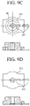
- FIG. 9A, FIG. 9B , FIG. 9C and FIG. 9D is a view for describing a method of adjusting the radio frequency (RF) characteristics of the fixed connector according to an embodiment of the present invention.
- RF radio frequency
- the fixed connector 20 may adjust RF characteristics through the shape of the dielectric 300.
- at least one circular groove H4 as in FIGS. 9A and 9B may be formed in a bottom surface corresponding to the substrate 10 or an annular groove H5 may be formed to be open in a direction in which the second signal pin 220 disposed on the substrate 10 is oriented as in FIG. 9C on the basis of a center of the first signal pin 210, which is inserted into the body 100, among the signal pin 200.
- the grooves H4 and H5 are formed in the dielectric 300, an air hole may be formed in the fixed connector 20, and the RF characteristics can be adjusted according to the size (the volume) of the air hole.
- the groove may not be formed in the bottom surface of the dielectric 300 as in FIG. 9D depending on process convenience rather than the RF characteristics.
- a plurality of circular grooves H4 may be arranged in a circular shape based on the center of the first signal pin 210.
- the number of annular grooves H5 may be two or more.
- a plurality of grooves H5 having a ring shape or an arcuate shape may be arranged in a circular shape based on the center of the first signal pin 210, and various ring-shaped grooves H5, which are not limited thereto, may be formed in the dielectric 300.
- the shape of the bottom surface of the dielectric 300 may extend as in FIG. 9B according to the length of the signal electrode SE formed on the substrate 10 to prevent lead-rising of the fixed connector 20.
- the dielectric 300 may extend in a direction opposite to a direction toward the second signal pin 220 as in FIGS. 9C and 9D to adjust the RF characteristics.
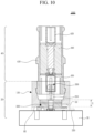
- FIG. 10 is a view for describing a method of improving the characteristics of the connector assembly according to an embodiment of the present invention.
- the second groove H2 may be formed such that the second signal pin 220, among the signal pin 200, disposed on the substrate 10 passes therethrough.
- An air gap E in which the body 100 and the substrate 10 may be spaced apart from each other may be formed in the second groove H2. That is, the air gap E may be formed between the body 100 and the dielectric 300 on a region in which the second signal pin 220 is disposed.
- the power capacity of the connector assembly 1000 can be increased, heat generation of the connector assembly 1000 can be reduced, and the influence on the power capacity of the connector assembly 1000 can be minimized even when the amount of lead applied to the second signal pin 220 is increased, as compared to a state in which there is no air gap E.
- a gap (the height of the air gap E) between the body 100 and the dielectric 300 may be adjusted, and as needed, the height of the dielectric 300 is increased to come into contact with the body 100, and thus no gap may be present between the body 100 and the dielectric 300.
- the length of the signal pin 200 may be longer due to the presence of the second groove H2, the return loss and insertion loss values may be maintained even when the signal pin 200 has an L shape.
- the first groove H1 may be formed on the other side of the bottom surface of the body 100 facing the second groove H2 formed on one side of the bottom surface of the body 100.
- the second groove H2 may have a width greater than that of the first groove H1 or the height of the air gap formed through the second groove H2 may be greater than the height of the air gap formed through the first groove H1.
Landscapes
- Coupling Device And Connection With Printed Circuit (AREA)
- Multi-Conductor Connections (AREA)
Applications Claiming Priority (2)
| Application Number | Priority Date | Filing Date | Title |
|---|---|---|---|
| KR20210126269 | 2021-09-24 | ||
| KR1020220014413A KR102496373B1 (ko) | 2021-09-24 | 2022-02-03 | 고정 커넥터 및 이를 포함하는 커넥터 조립체 |
Publications (3)
| Publication Number | Publication Date |
|---|---|
| EP4156418A2 true EP4156418A2 (de) | 2023-03-29 |
| EP4156418A3 EP4156418A3 (de) | 2023-06-07 |
| EP4156418B1 EP4156418B1 (de) | 2025-07-23 |
Family
ID=83438883
Family Applications (1)
| Application Number | Title | Priority Date | Filing Date |
|---|---|---|---|
| EP22197307.6A Active EP4156418B1 (de) | 2021-09-24 | 2022-09-23 | Fester verbinder und verbinderanordnung damit |
Country Status (3)
| Country | Link |
|---|---|
| US (1) | US12394922B2 (de) |
| EP (1) | EP4156418B1 (de) |
| CN (1) | CN115864029B (de) |
Cited By (1)
| Publication number | Priority date | Publication date | Assignee | Title |
|---|---|---|---|---|
| EP4712274A1 (de) * | 2024-09-16 | 2026-03-18 | TE Connectivity Solutions GmbH | Invertierter koaxialer substratverbinder |
Families Citing this family (3)
| Publication number | Priority date | Publication date | Assignee | Title |
|---|---|---|---|---|
| JP6780689B2 (ja) * | 2018-11-21 | 2020-11-04 | I−Pex株式会社 | 電気コネクタ及びコネクタ装置 |
| CN115864029B (zh) * | 2021-09-24 | 2024-03-05 | 吉佳蓝科技股份有限公司 | 固定连接器以及具备其的连接器组件 |
| USD1056853S1 (en) * | 2021-11-01 | 2025-01-07 | Gigalane Co., Ltd. | Rf connector |
Citations (3)
| Publication number | Priority date | Publication date | Assignee | Title |
|---|---|---|---|---|
| KR101311724B1 (ko) | 2012-04-05 | 2013-09-26 | 주식회사 기가레인 | 커넥터 조립체 |
| KR101898940B1 (ko) | 2016-11-08 | 2018-10-04 | 주식회사 에이스테크놀로지 | 기판연결용 커넥터 |
| KR101938537B1 (ko) | 2015-10-07 | 2019-04-11 | 로젠버거 호흐프리쿠벤츠테흐닉 게엠베하 운트 코. 카게 | 플러그 및 소켓 커넥터 |
Family Cites Families (27)
| Publication number | Priority date | Publication date | Assignee | Title |
|---|---|---|---|---|
| US6164977A (en) * | 1998-02-09 | 2000-12-26 | Itt Manufacturing Enterprises, Inc. | Standoff board-mounted coaxial connector |
| US6264475B1 (en) * | 1999-05-19 | 2001-07-24 | Antaya Technologies Corporation | Coaxial receptace |
| US6474995B1 (en) * | 2001-10-30 | 2002-11-05 | Hon Hai Precision Ind. Co., Ltd. | Low profile RF connector and method of manufacturing the RF connector |
| JP3834309B2 (ja) | 2002-12-26 | 2006-10-18 | ヒロセ電機株式会社 | 同軸電気コネクタ |
| DE10312515A1 (de) * | 2003-03-20 | 2004-10-07 | Ims Connector Systems Gmbh | Steckverbinder zum elektrischen Verbinden einer planaren Struktur mit einer koaxialen Struktur |
| US6776621B1 (en) * | 2003-08-27 | 2004-08-17 | Itt Manufacturing Enterprises, Inc. | Board mounted coax connector assembly |
| US6905364B2 (en) * | 2003-09-17 | 2005-06-14 | Osram Sylvania, Inc. | High frequency right angle connector |
| KR200404096Y1 (ko) * | 2005-09-29 | 2005-12-19 | (주)애드컴 | 스위치 기능을 갖는 안테나 연결용 커넥터 |
| JP4382834B2 (ja) * | 2007-04-25 | 2009-12-16 | ヒロセ電機株式会社 | 回路基板用同軸電気コネクタ |
| US7651334B2 (en) * | 2007-11-02 | 2010-01-26 | Hon Hai Precision Ind. Co., Ltd. | Coaxial electrical connector |
| JP4325885B1 (ja) | 2009-03-27 | 2009-09-02 | 株式会社アイペックス | 同軸コネクタ装置 |
| KR101311738B1 (ko) | 2012-01-18 | 2013-09-26 | 주식회사 기가레인 | 인쇄회로기판 결합 커넥터 및 인쇄회로기판과 커넥터 간 결합방법 |
| US8911240B2 (en) * | 2013-03-15 | 2014-12-16 | Samtec, Inc. | Right-angle board-mounted connectors |
| TWM464857U (zh) * | 2013-05-14 | 2013-11-01 | yi-fang Zhuang | 電連接器 |
| CN203536663U (zh) * | 2013-09-11 | 2014-04-09 | 番禺得意精密电子工业有限公司 | 同轴连接器 |
| JP5748111B2 (ja) * | 2013-10-10 | 2015-07-15 | 第一精工株式会社 | 同軸コネクタ装置 |
| JP6588403B2 (ja) * | 2016-08-09 | 2019-10-09 | ヒロセ電機株式会社 | 同軸コネクタ |
| KR101922142B1 (ko) | 2017-07-20 | 2018-11-26 | 주식회사 엠피디 | 기판연결용 커넥터 |
| KR101926503B1 (ko) * | 2018-03-27 | 2018-12-07 | 주식회사 기가레인 | 신호 컨택부 및 그라운드 컨택부가 연동되는 기판 메이팅 커넥터 |
| KR102006134B1 (ko) | 2018-04-12 | 2019-08-01 | 주식회사 엠피디 | 기판 연결용 커넥터 |
| KR101974785B1 (ko) * | 2018-07-10 | 2019-05-02 | 주식회사 기가레인 | 결합 높이가 감소된 기판 메이팅 커넥터 |
| KR102897976B1 (ko) * | 2019-12-27 | 2025-12-16 | 주식회사 기가레인 | 기판 메이팅 커넥터 |
| JP7344150B2 (ja) * | 2020-02-10 | 2023-09-13 | ヒロセ電機株式会社 | 同軸電気コネクタの製造方法 |
| KR102375210B1 (ko) * | 2020-12-21 | 2022-03-16 | 주식회사 기가레인 | 커넥터 및 이를 포함하는 보드 접속 어셈블리 |
| EP4156420A4 (de) * | 2020-12-21 | 2024-07-24 | GigaLane Co., Ltd. | Plattensteckverbinder und plattenverbindungsanordnung damit |
| KR102309404B1 (ko) | 2021-02-01 | 2021-10-07 | 주식회사 엠피디 | 기판연결용 커넥터 |
| CN115864029B (zh) * | 2021-09-24 | 2024-03-05 | 吉佳蓝科技股份有限公司 | 固定连接器以及具备其的连接器组件 |
-
2022
- 2022-09-02 CN CN202211072382.XA patent/CN115864029B/zh active Active
- 2022-09-23 US US17/934,600 patent/US12394922B2/en active Active
- 2022-09-23 EP EP22197307.6A patent/EP4156418B1/de active Active
Patent Citations (3)
| Publication number | Priority date | Publication date | Assignee | Title |
|---|---|---|---|---|
| KR101311724B1 (ko) | 2012-04-05 | 2013-09-26 | 주식회사 기가레인 | 커넥터 조립체 |
| KR101938537B1 (ko) | 2015-10-07 | 2019-04-11 | 로젠버거 호흐프리쿠벤츠테흐닉 게엠베하 운트 코. 카게 | 플러그 및 소켓 커넥터 |
| KR101898940B1 (ko) | 2016-11-08 | 2018-10-04 | 주식회사 에이스테크놀로지 | 기판연결용 커넥터 |
Cited By (1)
| Publication number | Priority date | Publication date | Assignee | Title |
|---|---|---|---|---|
| EP4712274A1 (de) * | 2024-09-16 | 2026-03-18 | TE Connectivity Solutions GmbH | Invertierter koaxialer substratverbinder |
Also Published As
| Publication number | Publication date |
|---|---|
| CN115864029B (zh) | 2024-03-05 |
| CN115864029A (zh) | 2023-03-28 |
| EP4156418A3 (de) | 2023-06-07 |
| US12394922B2 (en) | 2025-08-19 |
| US20230100478A1 (en) | 2023-03-30 |
| EP4156418B1 (de) | 2025-07-23 |
Similar Documents
| Publication | Publication Date | Title |
|---|---|---|
| EP4156418A2 (de) | Fester verbinder und verbinderanordnung damit | |
| US10164384B2 (en) | Coaxial connector | |
| US9620900B2 (en) | Coaxial connector with floating mechanism | |
| KR102494901B1 (ko) | 커넥터 조립체 및 커넥터 | |
| JP5178847B2 (ja) | Rf用プラグコネクタ、rf用リセプタクルコネクタ、及び、rf用コネクタ | |
| EP3547459A1 (de) | Leiterplattengegenstecker, in dem signalkontakteinheit und bodenkontakteinheit verriegelt sind | |
| EP3547460B1 (de) | Leiterplattengegenstecker | |
| CN108092015B (zh) | 缆线、缆线组件以及将缆线连接到基板的方法 | |
| KR101966410B1 (ko) | 캐비티 필터 | |
| US12100912B2 (en) | Connector with shielded terminals | |
| CN103138084A (zh) | 同轴连接器插头及其制造方法 | |
| US11929550B2 (en) | Wireless communication connector and communication module comprising same | |
| CN108448213A (zh) | 空腔滤波器 | |
| KR20020008777A (ko) | 동축 커넥터 및 이를 포함하는 통신 장치 | |
| US20060105640A1 (en) | Low profile circuit board connector | |
| KR102309404B1 (ko) | 기판연결용 커넥터 | |
| KR102496373B1 (ko) | 고정 커넥터 및 이를 포함하는 커넥터 조립체 | |
| EP3787127B1 (de) | Schirmverbinder | |
| JP4049230B2 (ja) | マイクロ波デバイス | |
| KR20180054230A (ko) | 동축 커넥터 플러그 및 이를 포함하는 rf 커넥터 | |
| EP2779326B1 (de) | Elektrischer verbinder mit einem Shunt und Verbinderanordnung mit zwei solchen Steckverbindern | |
| US20060227061A1 (en) | Omni-directional collinear antenna | |
| WO2025249010A1 (ja) | 電子装置 | |
| KR20230156858A (ko) | 커넥터 어셈블리 |
Legal Events
| Date | Code | Title | Description |
|---|---|---|---|
| PUAI | Public reference made under article 153(3) epc to a published international application that has entered the european phase |
Free format text: ORIGINAL CODE: 0009012 |
|
| STAA | Information on the status of an ep patent application or granted ep patent |
Free format text: STATUS: REQUEST FOR EXAMINATION WAS MADE |
|
| 17P | Request for examination filed |
Effective date: 20220923 |
|
| AK | Designated contracting states |
Kind code of ref document: A2 Designated state(s): AL AT BE BG CH CY CZ DE DK EE ES FI FR GB GR HR HU IE IS IT LI LT LU LV MC MK MT NL NO PL PT RO RS SE SI SK SM TR |
|
| PUAL | Search report despatched |
Free format text: ORIGINAL CODE: 0009013 |
|
| AK | Designated contracting states |
Kind code of ref document: A3 Designated state(s): AL AT BE BG CH CY CZ DE DK EE ES FI FR GB GR HR HU IE IS IT LI LT LU LV MC MK MT NL NO PL PT RO RS SE SI SK SM TR |
|
| RIC1 | Information provided on ipc code assigned before grant |
Ipc: H01R 103/00 20060101ALN20230502BHEP Ipc: H01R 12/91 20110101ALN20230502BHEP Ipc: H01R 24/50 20110101ALI20230502BHEP Ipc: H01R 12/70 20110101AFI20230502BHEP |
|
| RBV | Designated contracting states (corrected) |
Designated state(s): AL AT BE BG CH CY CZ DE DK EE ES FI FR GB GR HR HU IE IS IT LI LT LU LV MC MK MT NL NO PL PT RO RS SE SI SK SM TR |
|
| GRAP | Despatch of communication of intention to grant a patent |
Free format text: ORIGINAL CODE: EPIDOSNIGR1 |
|
| STAA | Information on the status of an ep patent application or granted ep patent |
Free format text: STATUS: GRANT OF PATENT IS INTENDED |
|
| RIC1 | Information provided on ipc code assigned before grant |
Ipc: H01R 103/00 20060101ALN20250227BHEP Ipc: H01R 12/91 20110101ALN20250227BHEP Ipc: H01R 24/50 20110101ALI20250227BHEP Ipc: H01R 12/70 20110101AFI20250227BHEP |
|
| RIC1 | Information provided on ipc code assigned before grant |
Ipc: H01R 103/00 20060101ALN20250320BHEP Ipc: H01R 12/91 20110101ALN20250320BHEP Ipc: H01R 24/50 20110101ALI20250320BHEP Ipc: H01R 12/70 20110101AFI20250320BHEP |
|
| INTG | Intention to grant announced |
Effective date: 20250401 |
|
| RIC1 | Information provided on ipc code assigned before grant |
Ipc: H01R 103/00 20060101ALN20250324BHEP Ipc: H01R 12/91 20110101ALN20250324BHEP Ipc: H01R 24/50 20110101ALI20250324BHEP Ipc: H01R 12/70 20110101AFI20250324BHEP |
|
| GRAS | Grant fee paid |
Free format text: ORIGINAL CODE: EPIDOSNIGR3 |
|
| GRAA | (expected) grant |
Free format text: ORIGINAL CODE: 0009210 |
|
| STAA | Information on the status of an ep patent application or granted ep patent |
Free format text: STATUS: THE PATENT HAS BEEN GRANTED |
|
| AK | Designated contracting states |
Kind code of ref document: B1 Designated state(s): AL AT BE BG CH CY CZ DE DK EE ES FI FR GB GR HR HU IE IS IT LI LT LU LV MC MK MT NL NO PL PT RO RS SE SI SK SM TR |
|
| REG | Reference to a national code |
Ref country code: GB Ref legal event code: FG4D |
|
| REG | Reference to a national code |
Ref country code: CH Ref legal event code: EP |
|
| REG | Reference to a national code |
Ref country code: DE Ref legal event code: R096 Ref document number: 602022017959 Country of ref document: DE |
|
| REG | Reference to a national code |
Ref country code: IE Ref legal event code: FG4D |
|
| PGFP | Annual fee paid to national office [announced via postgrant information from national office to epo] |
Ref country code: AT Payment date: 20251020 Year of fee payment: 4 |
|
| REG | Reference to a national code |
Ref country code: NL Ref legal event code: MP Effective date: 20250723 |
|
| PG25 | Lapsed in a contracting state [announced via postgrant information from national office to epo] |
Ref country code: PT Free format text: LAPSE BECAUSE OF FAILURE TO SUBMIT A TRANSLATION OF THE DESCRIPTION OR TO PAY THE FEE WITHIN THE PRESCRIBED TIME-LIMIT Effective date: 20251124 |
|
| PG25 | Lapsed in a contracting state [announced via postgrant information from national office to epo] |
Ref country code: NL Free format text: LAPSE BECAUSE OF FAILURE TO SUBMIT A TRANSLATION OF THE DESCRIPTION OR TO PAY THE FEE WITHIN THE PRESCRIBED TIME-LIMIT Effective date: 20250723 |
|
| REG | Reference to a national code |
Ref country code: AT Ref legal event code: MK05 Ref document number: 1817433 Country of ref document: AT Kind code of ref document: T Effective date: 20250723 |
|
| PG25 | Lapsed in a contracting state [announced via postgrant information from national office to epo] |
Ref country code: IS Free format text: LAPSE BECAUSE OF FAILURE TO SUBMIT A TRANSLATION OF THE DESCRIPTION OR TO PAY THE FEE WITHIN THE PRESCRIBED TIME-LIMIT Effective date: 20251123 |
|
| PG25 | Lapsed in a contracting state [announced via postgrant information from national office to epo] |
Ref country code: NO Free format text: LAPSE BECAUSE OF FAILURE TO SUBMIT A TRANSLATION OF THE DESCRIPTION OR TO PAY THE FEE WITHIN THE PRESCRIBED TIME-LIMIT Effective date: 20251023 |
|
| REG | Reference to a national code |
Ref country code: LT Ref legal event code: MG9D |
|
| PG25 | Lapsed in a contracting state [announced via postgrant information from national office to epo] |
Ref country code: AT Free format text: LAPSE BECAUSE OF FAILURE TO SUBMIT A TRANSLATION OF THE DESCRIPTION OR TO PAY THE FEE WITHIN THE PRESCRIBED TIME-LIMIT Effective date: 20250723 |
|
| PG25 | Lapsed in a contracting state [announced via postgrant information from national office to epo] |
Ref country code: FI Free format text: LAPSE BECAUSE OF FAILURE TO SUBMIT A TRANSLATION OF THE DESCRIPTION OR TO PAY THE FEE WITHIN THE PRESCRIBED TIME-LIMIT Effective date: 20250723 |
|
| PG25 | Lapsed in a contracting state [announced via postgrant information from national office to epo] |
Ref country code: HR Free format text: LAPSE BECAUSE OF FAILURE TO SUBMIT A TRANSLATION OF THE DESCRIPTION OR TO PAY THE FEE WITHIN THE PRESCRIBED TIME-LIMIT Effective date: 20250723 |
|
| PG25 | Lapsed in a contracting state [announced via postgrant information from national office to epo] |
Ref country code: GR Free format text: LAPSE BECAUSE OF FAILURE TO SUBMIT A TRANSLATION OF THE DESCRIPTION OR TO PAY THE FEE WITHIN THE PRESCRIBED TIME-LIMIT Effective date: 20251024 |
|
| PG25 | Lapsed in a contracting state [announced via postgrant information from national office to epo] |
Ref country code: SE Free format text: LAPSE BECAUSE OF FAILURE TO SUBMIT A TRANSLATION OF THE DESCRIPTION OR TO PAY THE FEE WITHIN THE PRESCRIBED TIME-LIMIT Effective date: 20250723 |
|
| PG25 | Lapsed in a contracting state [announced via postgrant information from national office to epo] |
Ref country code: LV Free format text: LAPSE BECAUSE OF FAILURE TO SUBMIT A TRANSLATION OF THE DESCRIPTION OR TO PAY THE FEE WITHIN THE PRESCRIBED TIME-LIMIT Effective date: 20250723 |
|
| PG25 | Lapsed in a contracting state [announced via postgrant information from national office to epo] |
Ref country code: BG Free format text: LAPSE BECAUSE OF FAILURE TO SUBMIT A TRANSLATION OF THE DESCRIPTION OR TO PAY THE FEE WITHIN THE PRESCRIBED TIME-LIMIT Effective date: 20250723 Ref country code: PL Free format text: LAPSE BECAUSE OF FAILURE TO SUBMIT A TRANSLATION OF THE DESCRIPTION OR TO PAY THE FEE WITHIN THE PRESCRIBED TIME-LIMIT Effective date: 20250723 |
|
| PG25 | Lapsed in a contracting state [announced via postgrant information from national office to epo] |
Ref country code: RS Free format text: LAPSE BECAUSE OF FAILURE TO SUBMIT A TRANSLATION OF THE DESCRIPTION OR TO PAY THE FEE WITHIN THE PRESCRIBED TIME-LIMIT Effective date: 20251023 |
|
| PG25 | Lapsed in a contracting state [announced via postgrant information from national office to epo] |
Ref country code: ES Free format text: LAPSE BECAUSE OF FAILURE TO SUBMIT A TRANSLATION OF THE DESCRIPTION OR TO PAY THE FEE WITHIN THE PRESCRIBED TIME-LIMIT Effective date: 20250723 |
|
| PG25 | Lapsed in a contracting state [announced via postgrant information from national office to epo] |
Ref country code: RO Free format text: LAPSE BECAUSE OF FAILURE TO SUBMIT A TRANSLATION OF THE DESCRIPTION OR TO PAY THE FEE WITHIN THE PRESCRIBED TIME-LIMIT Effective date: 20250723 |
|
| PG25 | Lapsed in a contracting state [announced via postgrant information from national office to epo] |
Ref country code: SM Free format text: LAPSE BECAUSE OF FAILURE TO SUBMIT A TRANSLATION OF THE DESCRIPTION OR TO PAY THE FEE WITHIN THE PRESCRIBED TIME-LIMIT Effective date: 20250723 |
|
| PG25 | Lapsed in a contracting state [announced via postgrant information from national office to epo] |
Ref country code: DK Free format text: LAPSE BECAUSE OF FAILURE TO SUBMIT A TRANSLATION OF THE DESCRIPTION OR TO PAY THE FEE WITHIN THE PRESCRIBED TIME-LIMIT Effective date: 20250723 |
|
| PG25 | Lapsed in a contracting state [announced via postgrant information from national office to epo] |
Ref country code: IT Free format text: LAPSE BECAUSE OF FAILURE TO SUBMIT A TRANSLATION OF THE DESCRIPTION OR TO PAY THE FEE WITHIN THE PRESCRIBED TIME-LIMIT Effective date: 20250723 |