EP4156165A2 - Methods for driving electro-optic displays - Google Patents
Methods for driving electro-optic displays Download PDFInfo
- Publication number
- EP4156165A2 EP4156165A2 EP22202038.0A EP22202038A EP4156165A2 EP 4156165 A2 EP4156165 A2 EP 4156165A2 EP 22202038 A EP22202038 A EP 22202038A EP 4156165 A2 EP4156165 A2 EP 4156165A2
- Authority
- EP
- European Patent Office
- Prior art keywords
- pixels
- display
- white
- update
- transitions
- Prior art date
- Legal status (The legal status is an assumption and is not a legal conclusion. Google has not performed a legal analysis and makes no representation as to the accuracy of the status listed.)
- Pending
Links
- 238000000034 method Methods 0.000 title claims abstract description 87
- 230000007704 transition Effects 0.000 claims abstract description 131
- 230000003287 optical effect Effects 0.000 claims abstract description 51
- 230000008859 change Effects 0.000 abstract description 8
- 230000036961 partial effect Effects 0.000 description 41
- 230000000694 effects Effects 0.000 description 29
- 239000012530 fluid Substances 0.000 description 12
- 239000002245 particle Substances 0.000 description 12
- 230000005684 electric field Effects 0.000 description 9
- 238000005562 fading Methods 0.000 description 9
- 239000000463 material Substances 0.000 description 9
- 230000002829 reductive effect Effects 0.000 description 7
- 238000013459 approach Methods 0.000 description 6
- 238000000576 coating method Methods 0.000 description 6
- 230000008569 process Effects 0.000 description 6
- 230000008901 benefit Effects 0.000 description 5
- 239000011248 coating agent Substances 0.000 description 5
- 230000006872 improvement Effects 0.000 description 5
- 239000011159 matrix material Substances 0.000 description 5
- 239000002775 capsule Substances 0.000 description 4
- 230000002441 reversible effect Effects 0.000 description 4
- 230000015572 biosynthetic process Effects 0.000 description 3
- 238000005516 engineering process Methods 0.000 description 3
- 239000007788 liquid Substances 0.000 description 3
- 238000004519 manufacturing process Methods 0.000 description 3
- 230000004048 modification Effects 0.000 description 3
- 238000012986 modification Methods 0.000 description 3
- 238000007639 printing Methods 0.000 description 3
- 238000009877 rendering Methods 0.000 description 3
- 230000005540 biological transmission Effects 0.000 description 2
- 230000007547 defect Effects 0.000 description 2
- 238000010586 diagram Methods 0.000 description 2
- 238000003384 imaging method Methods 0.000 description 2
- 230000009467 reduction Effects 0.000 description 2
- 238000009736 wetting Methods 0.000 description 2
- 239000004988 Nematic liquid crystal Substances 0.000 description 1
- 241000872198 Serjania polyphylla Species 0.000 description 1
- 208000033853 acromesomelic dysplasia 4 Diseases 0.000 description 1
- 230000009471 action Effects 0.000 description 1
- 230000002730 additional effect Effects 0.000 description 1
- 239000000853 adhesive Substances 0.000 description 1
- 230000001070 adhesive effect Effects 0.000 description 1
- 230000002411 adverse Effects 0.000 description 1
- 238000007754 air knife coating Methods 0.000 description 1
- 238000003491 array Methods 0.000 description 1
- 239000011230 binding agent Substances 0.000 description 1
- 230000001413 cellular effect Effects 0.000 description 1
- 230000001427 coherent effect Effects 0.000 description 1
- 238000012790 confirmation Methods 0.000 description 1
- 238000012937 correction Methods 0.000 description 1
- 230000008878 coupling Effects 0.000 description 1
- 238000010168 coupling process Methods 0.000 description 1
- 238000005859 coupling reaction Methods 0.000 description 1
- 238000007766 curtain coating Methods 0.000 description 1
- 230000003247 decreasing effect Effects 0.000 description 1
- 238000013461 design Methods 0.000 description 1
- 238000007607 die coating method Methods 0.000 description 1
- 238000003618 dip coating Methods 0.000 description 1
- 238000001652 electrophoretic deposition Methods 0.000 description 1
- 238000002474 experimental method Methods 0.000 description 1
- 238000007765 extrusion coating Methods 0.000 description 1
- 238000007756 gravure coating Methods 0.000 description 1
- 238000007641 inkjet printing Methods 0.000 description 1
- 230000002427 irreversible effect Effects 0.000 description 1
- 238000009685 knife-over-roll coating Methods 0.000 description 1
- 238000003475 lamination Methods 0.000 description 1
- 239000004973 liquid crystal related substance Substances 0.000 description 1
- 235000020281 long black Nutrition 0.000 description 1
- 230000007774 longterm Effects 0.000 description 1
- 238000004020 luminiscence type Methods 0.000 description 1
- 230000014759 maintenance of location Effects 0.000 description 1
- 230000005499 meniscus Effects 0.000 description 1
- 239000003094 microcapsule Substances 0.000 description 1
- 238000001000 micrograph Methods 0.000 description 1
- 230000003278 mimic effect Effects 0.000 description 1
- 230000037361 pathway Effects 0.000 description 1
- 230000003334 potential effect Effects 0.000 description 1
- 238000012545 processing Methods 0.000 description 1
- 230000000717 retained effect Effects 0.000 description 1
- 238000007763 reverse roll coating Methods 0.000 description 1
- 238000007650 screen-printing Methods 0.000 description 1
- 238000004528 spin coating Methods 0.000 description 1
- 238000005507 spraying Methods 0.000 description 1
- 239000000758 substrate Substances 0.000 description 1
- 238000007651 thermal printing Methods 0.000 description 1
- 230000001052 transient effect Effects 0.000 description 1
- 230000000007 visual effect Effects 0.000 description 1
- 239000002023 wood Substances 0.000 description 1
Images


Classifications
-
- G—PHYSICS
- G09—EDUCATION; CRYPTOGRAPHY; DISPLAY; ADVERTISING; SEALS
- G09G—ARRANGEMENTS OR CIRCUITS FOR CONTROL OF INDICATING DEVICES USING STATIC MEANS TO PRESENT VARIABLE INFORMATION
- G09G3/00—Control arrangements or circuits, of interest only in connection with visual indicators other than cathode-ray tubes
- G09G3/20—Control arrangements or circuits, of interest only in connection with visual indicators other than cathode-ray tubes for presentation of an assembly of a number of characters, e.g. a page, by composing the assembly by combination of individual elements arranged in a matrix no fixed position being assigned to or needed to be assigned to the individual characters or partial characters
- G09G3/34—Control arrangements or circuits, of interest only in connection with visual indicators other than cathode-ray tubes for presentation of an assembly of a number of characters, e.g. a page, by composing the assembly by combination of individual elements arranged in a matrix no fixed position being assigned to or needed to be assigned to the individual characters or partial characters by control of light from an independent source
- G09G3/3433—Control arrangements or circuits, of interest only in connection with visual indicators other than cathode-ray tubes for presentation of an assembly of a number of characters, e.g. a page, by composing the assembly by combination of individual elements arranged in a matrix no fixed position being assigned to or needed to be assigned to the individual characters or partial characters by control of light from an independent source using light modulating elements actuated by an electric field and being other than liquid crystal devices and electrochromic devices
- G09G3/344—Control arrangements or circuits, of interest only in connection with visual indicators other than cathode-ray tubes for presentation of an assembly of a number of characters, e.g. a page, by composing the assembly by combination of individual elements arranged in a matrix no fixed position being assigned to or needed to be assigned to the individual characters or partial characters by control of light from an independent source using light modulating elements actuated by an electric field and being other than liquid crystal devices and electrochromic devices based on particles moving in a fluid or in a gas, e.g. electrophoretic devices
-
- G—PHYSICS
- G09—EDUCATION; CRYPTOGRAPHY; DISPLAY; ADVERTISING; SEALS
- G09G—ARRANGEMENTS OR CIRCUITS FOR CONTROL OF INDICATING DEVICES USING STATIC MEANS TO PRESENT VARIABLE INFORMATION
- G09G2300/00—Aspects of the constitution of display devices
- G09G2300/04—Structural and physical details of display devices
- G09G2300/0469—Details of the physics of pixel operation
- G09G2300/0473—Use of light emitting or modulating elements having two or more stable states when no power is applied
-
- G—PHYSICS
- G09—EDUCATION; CRYPTOGRAPHY; DISPLAY; ADVERTISING; SEALS
- G09G—ARRANGEMENTS OR CIRCUITS FOR CONTROL OF INDICATING DEVICES USING STATIC MEANS TO PRESENT VARIABLE INFORMATION
- G09G2300/00—Aspects of the constitution of display devices
- G09G2300/06—Passive matrix structure, i.e. with direct application of both column and row voltages to the light emitting or modulating elements, other than LCD or OLED
-
- G—PHYSICS
- G09—EDUCATION; CRYPTOGRAPHY; DISPLAY; ADVERTISING; SEALS
- G09G—ARRANGEMENTS OR CIRCUITS FOR CONTROL OF INDICATING DEVICES USING STATIC MEANS TO PRESENT VARIABLE INFORMATION
- G09G2310/00—Command of the display device
- G09G2310/04—Partial updating of the display screen
-
- G—PHYSICS
- G09—EDUCATION; CRYPTOGRAPHY; DISPLAY; ADVERTISING; SEALS
- G09G—ARRANGEMENTS OR CIRCUITS FOR CONTROL OF INDICATING DEVICES USING STATIC MEANS TO PRESENT VARIABLE INFORMATION
- G09G2310/00—Command of the display device
- G09G2310/08—Details of timing specific for flat panels, other than clock recovery
-
- G—PHYSICS
- G09—EDUCATION; CRYPTOGRAPHY; DISPLAY; ADVERTISING; SEALS
- G09G—ARRANGEMENTS OR CIRCUITS FOR CONTROL OF INDICATING DEVICES USING STATIC MEANS TO PRESENT VARIABLE INFORMATION
- G09G2320/00—Control of display operating conditions
- G09G2320/02—Improving the quality of display appearance
- G09G2320/0209—Crosstalk reduction, i.e. to reduce direct or indirect influences of signals directed to a certain pixel of the displayed image on other pixels of said image, inclusive of influences affecting pixels in different frames or fields or sub-images which constitute a same image, e.g. left and right images of a stereoscopic display
-
- G—PHYSICS
- G09—EDUCATION; CRYPTOGRAPHY; DISPLAY; ADVERTISING; SEALS
- G09G—ARRANGEMENTS OR CIRCUITS FOR CONTROL OF INDICATING DEVICES USING STATIC MEANS TO PRESENT VARIABLE INFORMATION
- G09G2320/00—Control of display operating conditions
- G09G2320/02—Improving the quality of display appearance
- G09G2320/0257—Reduction of after-image effects
-
- G—PHYSICS
- G09—EDUCATION; CRYPTOGRAPHY; DISPLAY; ADVERTISING; SEALS
- G09G—ARRANGEMENTS OR CIRCUITS FOR CONTROL OF INDICATING DEVICES USING STATIC MEANS TO PRESENT VARIABLE INFORMATION
- G09G2320/00—Control of display operating conditions
- G09G2320/04—Maintaining the quality of display appearance
- G09G2320/041—Temperature compensation
-
- G—PHYSICS
- G09—EDUCATION; CRYPTOGRAPHY; DISPLAY; ADVERTISING; SEALS
- G09G—ARRANGEMENTS OR CIRCUITS FOR CONTROL OF INDICATING DEVICES USING STATIC MEANS TO PRESENT VARIABLE INFORMATION
- G09G2320/00—Control of display operating conditions
- G09G2320/04—Maintaining the quality of display appearance
- G09G2320/043—Preventing or counteracting the effects of ageing
- G09G2320/045—Compensation of drifts in the characteristics of light emitting or modulating elements
-
- G—PHYSICS
- G09—EDUCATION; CRYPTOGRAPHY; DISPLAY; ADVERTISING; SEALS
- G09G—ARRANGEMENTS OR CIRCUITS FOR CONTROL OF INDICATING DEVICES USING STATIC MEANS TO PRESENT VARIABLE INFORMATION
- G09G2320/00—Control of display operating conditions
- G09G2320/04—Maintaining the quality of display appearance
- G09G2320/043—Preventing or counteracting the effects of ageing
- G09G2320/048—Preventing or counteracting the effects of ageing using evaluation of the usage time
-
- G—PHYSICS
- G09—EDUCATION; CRYPTOGRAPHY; DISPLAY; ADVERTISING; SEALS
- G09G—ARRANGEMENTS OR CIRCUITS FOR CONTROL OF INDICATING DEVICES USING STATIC MEANS TO PRESENT VARIABLE INFORMATION
- G09G2340/00—Aspects of display data processing
- G09G2340/12—Overlay of images, i.e. displayed pixel being the result of switching between the corresponding input pixels
-
- Y—GENERAL TAGGING OF NEW TECHNOLOGICAL DEVELOPMENTS; GENERAL TAGGING OF CROSS-SECTIONAL TECHNOLOGIES SPANNING OVER SEVERAL SECTIONS OF THE IPC; TECHNICAL SUBJECTS COVERED BY FORMER USPC CROSS-REFERENCE ART COLLECTIONS [XRACs] AND DIGESTS
- Y02—TECHNOLOGIES OR APPLICATIONS FOR MITIGATION OR ADAPTATION AGAINST CLIMATE CHANGE
- Y02E—REDUCTION OF GREENHOUSE GAS [GHG] EMISSIONS, RELATED TO ENERGY GENERATION, TRANSMISSION OR DISTRIBUTION
- Y02E50/00—Technologies for the production of fuel of non-fossil origin
- Y02E50/10—Biofuels, e.g. bio-diesel
-
- Y—GENERAL TAGGING OF NEW TECHNOLOGICAL DEVELOPMENTS; GENERAL TAGGING OF CROSS-SECTIONAL TECHNOLOGIES SPANNING OVER SEVERAL SECTIONS OF THE IPC; TECHNICAL SUBJECTS COVERED BY FORMER USPC CROSS-REFERENCE ART COLLECTIONS [XRACs] AND DIGESTS
- Y02—TECHNOLOGIES OR APPLICATIONS FOR MITIGATION OR ADAPTATION AGAINST CLIMATE CHANGE
- Y02E—REDUCTION OF GREENHOUSE GAS [GHG] EMISSIONS, RELATED TO ENERGY GENERATION, TRANSMISSION OR DISTRIBUTION
- Y02E50/00—Technologies for the production of fuel of non-fossil origin
- Y02E50/30—Fuel from waste, e.g. synthetic alcohol or diesel
Definitions
- the present invention relates to methods for driving electro-optic displays, especially bistable electro-optic displays, and to apparatus for use in such methods. More specifically, this invention relates to driving methods which may allow for reduced "ghosting" and edge effects, and reduced flashing in such displays.
- This invention is especially, but not exclusively, intended for use with particle-based electrophoretic displays in which one or more types of electrically charged particles are present in a fluid and are moved through the fluid under the influence of an electric field to change the appearance of the display.
- optical property is typically color perceptible to the human eye, it may be another optical property, such as optical transmission, reflectance, luminescence or, in the case of displays intended for machine reading, pseudo-color in the sense of a change in reflectance of electromagnetic wavelengths outside the visible range.
- gray state is used herein in its conventional meaning in the imaging art to refer to a state intermediate two extreme optical states of a pixel, and does not necessarily imply a black-white transition between these two extreme states.
- E Ink patents and published applications referred to below describe electrophoretic displays in which the extreme states are white and deep blue, so that an intermediate "gray state” would actually be pale blue. Indeed, as already mentioned, the change in optical state may not be a color change at all.
- black and “white” may be used hereinafter to refer to the two extreme optical states of a display, and should be understood as normally including extreme optical states which are not strictly black and white, for example the aforementioned white and dark blue states.
- the term “monochrome” may be used hereinafter to denote a drive scheme which only drives pixels to their two extreme optical states with no intervening gray states.
- bistable and “bistability” are used herein in their conventional meaning in the art to refer to displays comprising display elements having first and second display states differing in at least one optical property, and such that after any given element has been driven, by means of an addressing pulse of finite duration, to assume either its first or second display state, after the addressing pulse has terminated, that state will persist for at least several times, for example at least four times, the minimum duration of the addressing pulse required to change the state of the display element.
- addressing pulse of finite duration
- some particle-based electrophoretic displays capable of gray scale are stable not only in their extreme black and white states but also in their intermediate gray states, and the same is true of some other types of electro-optic displays.
- This type of display is properly called “multi-stable” rather than bistable, although for convenience the term “bistable” may be used herein to cover both bistable and multi-stable displays.
- impulse is used herein in its conventional meaning of the integral of voltage with respect to time.
- bistable electro-optic media act as charge transducers, and with such media an alternative definition of impulse, namely the integral of current over time (which is equal to the total charge applied) may be used.
- the appropriate definition of impulse should be used, depending on whether the medium acts as a voltage-time impulse transducer or a charge impulse transducer.
- waveform will be used to denote the entire voltage against time curve used to effect the transition from one specific initial gray level to a specific final gray level.
- waveform will comprise a plurality of waveform elements; where these elements are essentially rectangular (i.e., where a given element comprises application of a constant voltage for a period of time); the elements may be called "pulses” or "drive pulses”.
- drive scheme denotes a set of waveforms sufficient to effect all possible transitions between gray levels for a specific display.
- a display may make use of more than one drive scheme; for example, the aforementioned U. S. Patent No. 7,012,600 teaches that a drive scheme may need to be modified depending upon parameters such as the temperature of the display or the time for which it has been in operation during its lifetime, and thus a display may be provided with a plurality of different drive schemes to be used at differing temperature etc.
- a set of drive schemes used in this manner may be referred to as "a set of related drive schemes.” It is also possible, as described in several of the aforementioned MEDEOD applications, to use more than one drive scheme simultaneously in different areas of the same display, and a set of drive schemes used in this manner may be referred to as "a set of simultaneous drive schemes.”
- Electrophoretic media can use liquid or gaseous fluids; for gaseous fluids see, for example, Kitamura, T., et al., “Electrical toner movement for electronic paper-like display", IDW Japan, 2001, Paper HCS1-1 , and Yamaguchi, Y., et al., "Toner display using insulative particles charged triboelectrically", IDW Japan, 2001, Paper AMD4-4 ); U.S. Patent Publication No.
- the media may be encapsulated, comprising numerous small capsules, each of which itself comprises an internal phase containing electrophoretically-mobile particles suspended in a liquid suspending medium, and a capsule wall surrounding the internal phase.
- the capsules are themselves held within a polymeric binder to form a coherent layer positioned between two electrodes; see the aforementioned MIT and E Ink patents and applications.
- the walls surrounding the discrete microcapsules in an encapsulated electrophoretic medium may be replaced by a continuous phase, thus producing a so-called polymer-dispersed electrophoretic display, in which the electrophoretic medium comprises a plurality of discrete droplets of an electrophoretic fluid and a continuous phase of a polymeric material; see for example, U.S. Patent No. 6,866,760 .
- such polymer-dispersed electrophoretic media are regarded as sub-species of encapsulated electrophoretic media.
- microcell electrophoretic display in which the charged particles and the fluid are retained within a plurality of cavities formed within a carrier medium, typically a polymeric film; see, for example, U.S. Patents Nos. 6,672,921 and 6,788,449 .
- An encapsulated electrophoretic display typically does not suffer from the clustering and settling failure mode of traditional electrophoretic devices and provides further advantages, such as the ability to print or coat the display on a wide variety of flexible and rigid substrates.
- printing is intended to include all forms of printing and coating, including, but without limitation: pre-metered coatings such as patch die coating, slot or extrusion coating, slide or cascade coating, curtain coating; roll coating such as knife over roll coating, forward and reverse roll coating; gravure coating; dip coating; spray coating; meniscus coating; spin coating; brush coating; air knife coating; silk screen printing processes; electrostatic printing processes; thermal printing processes; ink jet printing processes; electrophoretic deposition (See U.S. Patent No. 7,339,715 ); and other similar techniques.)
- pre-metered coatings such as patch die coating, slot or extrusion coating, slide or cascade coating, curtain coating
- roll coating such as knife over roll coating, forward and reverse roll coating
- gravure coating dip coating
- spray coating meniscus coating
- spin coating brush
- electro-optic media may also be used in the displays of the present invention.
- LC displays liquid crystal
- Twisted nematic liquid crystals are not bi- or multi-stable but act as voltage transducers, so that applying a given electric field to a pixel of such a display produces a specific gray level at the pixel, regardless of the gray level previously present at the pixel.
- LC displays are only driven in one direction (from non-transmissive or "dark” to transmissive or “light”), the reverse transition from a lighter state to a darker one being effected by reducing or eliminating the electric field.
- bistable electro-optic displays act, to a first approximation, as impulse transducers, so that the final state of a pixel depends not only upon the electric field applied and the time for which this field is applied, but also upon the state of the pixel prior to the application of the electric field.
- the electro-optic medium used is bistable, to obtain a high-resolution display, individual pixels of a display must be addressable without interference from adjacent pixels.
- One way to achieve this objective is to provide an array of non-linear elements, such as transistors or diodes, with at least one non-linear element associated with each pixel, to produce an "active matrix" display.
- An addressing or pixel electrode, which addresses one pixel, is connected to an appropriate voltage source through the associated non-linear element.
- the non-linear element is a transistor
- the pixel electrode is connected to the drain of the transistor, and this arrangement will be assumed in the following description, although it is essentially arbitrary and the pixel electrode could be connected to the source of the transistor.
- the pixels are arranged in a two-dimensional array of rows and columns, such that any specific pixel is uniquely defined by the intersection of one specified row and one specified column.
- the sources of all the transistors in each column are connected to a single column electrode, while the gates of all the transistors in each row are connected to a single row electrode; again the assignment of sources to rows and gates to columns is conventional but essentially arbitrary, and could be reversed if desired.
- the row electrodes are connected to a row driver, which essentially ensures that at any given moment only one row is selected, i.e., that there is applied to the selected row electrode a voltage such as to ensure that all the transistors in the selected row are conductive, while there is applied to all other rows a voltage such as to ensure that all the transistors in these non-selected rows remain non-conductive.
- the column electrodes are connected to column drivers, which place upon the various column electrodes voltages selected to drive the pixels in the selected row to their desired optical states.
- the aforementioned voltages are relative to a common front electrode which is conventionally provided on the opposed side of the electro-optic medium from the non-linear array and extends across the whole display.) After a pre-selected interval known as the "line address time" the selected row is deselected, the next row is selected, and the voltages on the column drivers are changed so that the next line of the display is written. This process is repeated so that the entire display is written in a row-by-row manner.
- general grayscale image flow requires very precise control of applied impulse to give good results, and empirically it has been found that, in the present state of the technology of electro-optic displays, general grayscale image flow is infeasible in a commercial display.
- a display capable of more than two gray levels may make use of a gray scale drive scheme ("GSDS") which can effect transitions between all possible gray levels, and a monochrome drive scheme ("MDS") which effects transitions only between two gray levels, the MDS providing quicker rewriting of the display that the GSDS.
- GSDS gray scale drive scheme
- MDS monochrome drive scheme
- the MDS is used when all the pixels which are being changed during a rewriting of the display are effecting transitions only between the two gray levels used by the MDS.
- 7,119,772 describes a display in the form of an electronic book or similar device capable of displaying gray scale images and also capable of displaying a monochrome dialogue box which permits a user to enter text relating to the displayed images.
- a rapid MDS is used for quick updating of the dialogue box, thus providing the user with rapid confirmation of the text being entered.
- a slower GSDS is used.
- a display may make use of a GSDS simultaneously with a "direct update” drive scheme ("DUDS").
- the DUDS may have two or more than two gray levels, typically fewer than the GSDS, but the most important characteristic of a DUDS is that transitions are handled by a simple unidirectional drive from the initial gray level to the final gray level, as opposed to the "indirect" transitions often used in a GSDS, where in at least some transitions the pixel is driven from an initial gray level to one extreme optical state, then in the reverse direction to a final gray level (this type of waveform may for convenience be referred to as a "single rail bounce” waveform); in some cases, the transition may be effected by driving from the initial gray level to one extreme optical state, thence to the opposed extreme optical state, and only then to the final extreme optical state (this type of waveform may for convenience be referred to as a "double rail bounce” waveform) - see, for example, the drive scheme illustrated in Figures 11A and 11B of the
- Present electrophoretic displays may have an update time in grayscale mode of about two to three times the length of a saturation pulse (where "the length of a saturation pulse” is defined as the time period, at a specific voltage, that suffices to drive a pixel of a display from one extreme optical state to the other), or approximately 700-900 milliseconds, whereas a DUDS has a maximum update time equal to the length of the saturation pulse, or about 200-300 milliseconds.
- drive schemes may be divided into global drive schemes, where a drive voltage is applied to every pixel in the region to which the global update drive scheme (more accurately referred to as a "global complete” or “GC” drive scheme) is being applied (which may be the whole display or some defined portion thereof) and partial update drive schemes, where a drive voltage is applied only to pixels that are undergoing a non-zero transition (i.e., a transition in which the initial and final gray levels differ from each other), but no drive voltage is applied during zero transitions (in which the initial and final gray levels are the same).
- GC global complete
- partial update drive schemes where a drive voltage is applied only to pixels that are undergoing a non-zero transition (i.e., a transition in which the initial and final gray levels differ from each other), but no drive voltage is applied during zero transitions (in which the initial and final gray levels are the same).
- An intermediate form a drive scheme (designated a "global limited” or “GL” drive scheme) is similar to a GC drive scheme except that no drive voltage is applied to a pixel which is undergoing a zero, white-to-white transition.
- a display used as an electronic book reader displaying black text on a white background, there are numerous white pixels, especially in the margins and between lines of text which remain unchanged from one page of text to the next; hence, not rewriting these white pixels substantially reduces the apparent "flashiness" of the display rewriting.
- certain problems remain in this type of GL drive scheme.
- bistable electro-optic media are typically not completely bistable, and pixels placed in one extreme optical state gradually drift, over a period of minutes to hours, towards an intermediate gray level.
- pixels driven white slowly drift towards a light gray color.
- Edge ghosting is clearly visible for example after multiple text page updates followed by an update to a white page where the contour of the previous text will appear darker compared to the background. Hitherto, such edge effects (and the effects of color drift in undriven white pixels) have typically been removed by using a single GC update at intervals. Unfortunately, use of such an occasional GC update reintroduces the problem of a "flashy" update, and indeed the flashiness of the update may be heightened by the fact that the flashy update only occurs at long intervals.
- SGU selective general update
- One such technique involves driving an electro-optic display having a plurality of pixels using a first drive scheme, in which all pixels are driven at each transition, and a second drive scheme, in which pixels undergoing some transitions are not driven.
- the first drive scheme is applied to a non-zero minor proportion of the pixels during a first update of the display, while the second drive scheme is applied to the remaining pixels during the first update.
- the first drive scheme is applied to a different non-zero minor proportion of the pixels, while the second drive scheme is applied to the remaining pixels during the second update.
- the SGU method is applied to refreshing the white background surrounding text or an image, so that only a minor proportion of the pixels in the white background undergo updating during any one display update, but all pixels of the background are gradually updated so that drifting of the white background to a gray color is avoided without any need for a flashy update.
- an "F" waveform a special waveform for the individual pixels which are to undergo updating on each transition.
- BPPWWTDS balanced pulse pair white/white transition drive scheme
- BPPWWTDS balanced pulse pair white/white transition drive scheme
- the pixels to which the BPP is applied are selected such that the BPP is masked by other update activity.
- a second such technique denoted “white/white top-off pulse drive scheme” or “WWTOPDS”
- WWTOPDS white/white top-off pulse drive scheme
- top-off' pulse during white-to-white transitions in pixels which can be identified as likely to give rise to edge artifacts, and are in a spatio-temporal configuration such that the top-off pulse will be efficacious in erasing or reducing the edge artifact.
- T special waveform
- the T and F waveforms are normally only applied to pixels undergoing white-to-white transitions.
- the white-to-white waveform is empty (i.e., consists of a series of zero voltage pulses) whereas all other waveforms are not empty. Accordingly, when applicable the non-empty T and F waveforms replace the empty white-to-white waveforms in a global limited drive scheme.
- a partial update mode is a controller function by which, when active, a pixel is removed from the update pipeline if it is a zero transition. For example if the initial state of a pixel was gray level 7 and the final state is also gray level 7, then that pixel will not be assigned to a transition pipeline and will be free to participate in another subsequent update at any time.
- a partial update mode only areas in the next image buffer that differ from the current image buffer will be driven by the drive scheme. This is especially helpful when overlaying an item (such as an icon, cursor or menu over an existing image (typically text); the overlaid can be stamped into the image buffer and sent to the controller, but only the area of the overlaid item will flash.
- partial update behavior can also be expressed by drive scheme design.
- a global limited (GL) mode may have an empty white-to-white transition but non-empty gray-to-gray and black-to-black transitions, so a white background will not flash when overlaying a menu, but the non-white text would flash.
- Other waveform modes such as DU and GU have all empty zero-transitions. In this case the behavior of the display will be exactly as described for partial update mode, but with one important difference: the zero transition pixels are not removed from the pipeline and must be driven with zeros for the full duration of the update.
- a zero transition pixel may or may not be removed from the update pipeline (or alternatively, receive a zero transition waveform) depending on an algorithmic decision.
- This concept may be generalized in the following manner.
- Each pixel of the display has an associated flag indicating whether that pixel does or does not receive an appropriate waveform.
- the flags define a Partial Update Mask (PUM) for the whole image in which flags are set TRUE for pixels that are driven and FALSE for pixels which are not driven. Any pixel undergoing a non-zero transition has a TRUE flag, but pixels undergoing zero transitions may have TRUE or FALSE flags.
- PUM Partial Update Mask
- T- and F-transitions are used with partial updates.
- two additional device controller states are required to enable the T- and F-transitions.
- states 1-16 correspond to the normal 16 gray levels
- state 17 denotes a T transition
- state 18 an F transition.
- a drive scheme is defined to convert any one initial state into any one final state.
- the final image buffer is preprocessed to determine when to substitute state 17 or 18 for state 16 (corresponding to a white gray level) according to the algorithm being used.
- the preprocessed image is then sent to the display controller, where partial update logic is applied to remove pixels undergoing zero transitions from the update pipeline.
- Pixels undergoing 16->16 (normal white-to-white) transitions can be removed from the pipeline since that transition is empty in a GL mode. However, pixels undergoing 17->17 or 18->18 transitions should not be removed from the pipeline since it is possible that the algorithm would need to apply two T or two F transitions successively to the same pixel.
- One aspect of the present invention provides a means of achieving this aim in both the controller and waveform implementations.
- a more difficult issue is that the decisions to use T or F transitions on a pixel is based on the initial and final states of pixels adjacent to the pixel being considered; in particular, in some cases if neighboring pixels are undergoing non-zero transitions, the decision as to whether to use T or F transitions on the pixel being considered can be changed.
- the use of a partial update mode can thwart the ability of the algorithm to correctly identify neighboring pixels not undergoing non-zero transitions, which can lead to reduced efficacy or even the introduction of new artifacts.
- a controller may also make use of a "regional update mode"; this mode is similar to a partial update mode except that only pixels within a selected region of the display are placed on the update pipeline.
- a regional update mode can be considered to be a specific case of a selective partial update mode in which the Partial Update Mask is set to FALSE for any pixel outside of the selected region.
- regional updates require special handling, as described below, because typically only data for the selected region is transferred to the controller.
- a second aspect of the present invention relates to improving performance of displays at temperatures above room temperature, for example when a display in the form of an electronic book reader is being used outdoors in summer.
- US 2013/0194250 describes a "balanced pulse pair white/white transition drive scheme" or "BPPWWTDS".
- BPPWWTDS balanced pulse pair white/white transition drive scheme
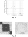
- Figure 1 shows that using a BPPWWTDS at 31°C and 35°C results in near zero improvement in edge ghosting scores after ten iterations with the use of a BPPWWTDS as compared with use of a drive scheme lacking balanced pulse pairs.
- the second aspect of the present invention relates to a DC imbalanced drive scheme intended to significantly reduce the aforementioned disadvantages of the BPPWWTDS.
- a third aspect of the invention relates to improved selective partial update drive schemes.
- electro-optic displays can be driven using partial updates, in which all pixels with any "self-transition" (zero transition) going from one image to the next (meaning that the pixel goes from a specific gray level in one image to the same specific gray level in the subsequent image), are not driven or (which amounts to the same thing) are driven with a waveform having a voltage list of zeros.
- Partial updates may be performed using a special waveform in which all the self-transitions are empty, i.e. filled with zeros, (usually called a "local” waveform) or using a device command that automatically detects self-transitions (known as a "partial update mode").
- Partial updates offer benefits in terms of reduced display flashiness. For example, with an initial image that has some text, a partial update may be used if we want to overlay a menu option on top of the text in order to avoid seeing the text updating on to itself.
- partial updates can create problems and/or be undesirable and incompatible with certain drive schemes. For example, consider a menu overlying existing text that is displayed and then dismissed as illustrated in Figures 9A-9C . If a partial update drive scheme is used, in text that overlaps with the border of the menu (as shown in Figure 9B ), all pixels with self-transition will be driven with an empty waveform, while their neighbors may be performing transitions with a non-zero waveform, e.g.
- electro-optic displays may also be driven using regional updates, in which only pixels within a selected region of the display (this region may be rectangular or of an arbitrary shape, including being selected pixel by pixel) are driven.
- the third aspect of the present invention relates to driving electro-optic displays using selective partial update drive schemes which permit retention of the benefits of partial update drive schemes in terms of reduced flashiness without creating text thinning/fading and with full compatibility with novel display modes for optimal display performance.
- a fourth aspect of the present invention relates to drift compensation, that is to say compensating for changes in the optical state of an electro-optic display with time.
- electrophoretic and similar electro-optic displays are bistable.
- the bistability of such displays is not unlimited in practice, a phenomenon known as image drift occurs, whereby pixels in or near extreme optical states tend to revert very slowly to intermediate gray levels; for example, black pixels gradually become dark gray and white pixels gradually become light gray.
- the white state drift is of particular interest because many electro-optic displays are most commonly used to display images with a white background; for example, electronic book readers normally mimic printed books by displaying black text on a white background.
- an electro-optic display is updated using a global limited drive scheme for a long periods of time without a full display refresh
- the white state drift becomes an essential part of the overall visual appearance of the display.
- the display will show areas of the display where the white state has been recently rewritten and other areas such as the background where the white state has not recently been rewritten and has thus been drifting for some time.
- ghosting effects are sufficiently annoying to most users that their presence a significant part in preventing the use of global limited drive schemes exclusively for long periods of time.
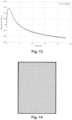
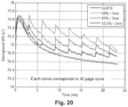
- Figure 13 shows an example of how the background white state of a display may drift over the course of about twenty minutes, resulting in significant ghosting as illustrated in Figure 14 , which shows an image after turning 45 text pages in low flash mode with 30 seconds between page turns.
- the text page has just been updated to a white page, and shows the ghosting resulting from "new" white in the text area versus "old" white in the background.
- the fourth aspect of the present invention relates to a method for driving a display which reduces or eliminates the problems caused by drift without producing the flash which would be perceived if all background pixels were updated simultaneously as in a global complete drive scheme.
- the first aspect of the present invention (which may hereinafter be referred to as the "Update Buffer Invention") provides a display controller (capable of controlling the operation of a bistable electro-optic display) having an update buffer, means for removing from the update buffer pixels which do not require updating during a given transition, means for receiving a list of states that should not be removed from the update buffer, and means to ensure that pixels having listed states are not removed from the update buffer.
- a display controller capable of controlling the operation of a bistable electro-optic display having an update buffer, means for removing from the update buffer pixels which do not require updating during a given transition, means for receiving a list of states that should not be removed from the update buffer, and means to ensure that pixels having listed states are not removed from the update buffer.
- the first aspect of the present invention also provides a display controller capable of controlling the operation of a bistable electro-optic display and having an update buffer, and means for removing from the update buffer pixels which do not require updating during a given transition, the controller having at least one special transition having two states associated therewith, means to determine when a pixel is undergoing a special transition immediately after a previous special transition, and means to insert into the update buffer the second state associated with the at least one special transition when a pixel is undergoing a special transition immediately after a previous special transition.
- the first aspect of the present invention also provides a drive scheme which achieves essentially the same result as the display controllers of the present invention already mentioned.
- a drive scheme zero transitions use empty waveform, but zero transitions corresponding to the special states use non-empty waveforms.
- This approach can work well for limited cases such as turning text pages, or going through an image sequence in which each successive image is always different from the previous one, or displaying and dismissing single items (icons, menus, etc.) that do not overlap with any of the non-white content of the initial image, or browsing up and down through an existing menu.
- the first aspect of the present invention also provides a modified algorithm for carrying out the SGU, BPPWWTDS or WWTOPDS drive schemes discussed above to take into account the non-flashing pixels that will be introduced by the partial update mode of the controller.
- the Partial Update Mask (PUM) value for each pixel must be computed according to the known controller algorithm. In the simplest case (standard partial update) the PUM is set to False if and only if the initial and final gray levels in the image buffer are the same.
- a modified algorithm is used which utilizes the PUM to determine local activity as prescribed by the algorithm.
- a second aspect of the present invention (which may hereinafter be referred to as the "BPPTOPWWTDS Invention") in effect combines the aforementioned BPPWWTDS and WWTOPDS by applying to pixels undergoing white-to-white transitions, identified as likely to give rise to edge artifacts, and in a spatio-temporal configuration such that the drive scheme of the present invention will be efficacious in erasing or reducing the edge artifact, a waveform which comprises at least one balanced pulse pair and at least one top-off pulse.
- This drive scheme of the present invention may for convenience be referred to a "balanced pulse pair/top-off pulse white/white transition drive scheme" or "BPPTOPWWTDS".
- the BPPTOPWWTDS of the present invention may be applied only when a display is operating in a particular temperature range, for example 30°C or higher, where a prior art BPPWWTDS is ineffective.
- the BPPTOPWWTDS waveform for white-to-white transitions may comprise a variable number of balanced pulse pairs at varying locations within the waveform and a variable number of top-off pulses which may vary in location within the waveform relative to the balanced pulse pairs.
- a single top-off pulse typically corresponds to one frame of white-going drive pulse.
- the top-off pulse(s) may be located before, after or between the balanced pulse pairs. It is generally preferred that there be only a single top-of pulse in the white-to-white transition waveform.
- a third aspect of the present invention (which may hereinafter be referred to as the "Overlay Invention") is intended to be applied when overlaying an item (an icon, menu, etc.) (typically a non-rectangular item) over existing text or image content followed by a removal of the item as generally illustrated in Figures 10A-10C .
- the overlay method of the present invention differs from standard partial updates drive schemes in that only the pixels in the region of the item perform transitions (including self-transitions) in order to avoid text thinning/fading for text that overlaps with the item and to avoid seeing the text outside that area flashing on to itself.
- One solution is to perform a regional update in the area of the item. Knowing the item geometry and location on the image, the controller can be used to perform a regional update for this area only.
- This simple overlay method of the present invention is not well adapted to cover situations in which the overlaid item is not completely opaque, i.e. the item does not fully fill a rectangle, or other area lying within the boundary of the overlaid item. If there are areas intended to be transparent within the overlaid item, they will also be fully updated by the regional drive scheme, which is not desirable for the reasons discussed above. An example of such a scenario is illustrated in Figures 11A-11C .
- a preferred method of the present invention updates only the pixels that overlap with the non-transparent (black as illustrated in Figures 11A-11C ) portions of the overlaid item (including such pixels undergoing self transitions), to produce the second and third images, thus reducing or eliminating visible text thinning/fading. All the pixels with self transitions that do not overlap with the non-transparent (black) portion of the overlaid item are updated with empty self transitions in order to reduce flashiness and avoid most of the text updating on to itself.
- the drive scheme may be a five-bit (32 gray level) drive scheme which takes advantage of the extra "empty" space inside the drive scheme to cope with the differing black-to-black transitions discussed above.
- a five-bit drive scheme allows 32 states, so that each of the 16 gray levels can use two different states. For example, assuming states 1 ⁇ 32, gray level black can use state 1 which is set with a non-empty self transition (1 ⁇ 1) as well as state 2 which is set with an empty self transition (2 ⁇ 2).
- Transition 1 ⁇ 2 is empty and transition 2 ⁇ 1 is a full non-empty black ⁇ black transition.
- the drive scheme algorithm determines the mask of pixels that must perform non-empty self-transitions as illustrated in Figures 12A-12C .
- black denotes the pixels performing self transitions from Figure 11A to Figure 11B
- Figure 12B black denotes all pixels that are underneath the overlaid item, i.e., all pixels that in non-transparent portions of the overlaid item.
- ANDing (in the Boolean sense of that term) the masks of Figures 12A and 12B produces the mask of Figure 12C , in which black denotes all pixels performing self transitions that need to be updated with a non-empty waveform.
- gray level black pixels in the second image are processed so that all the black pixels in Figure 12C stay in state 1, while all other black pixels become state 2.
- This mask-based algorithm allows all 16 gray levels to perform empty self transitions in some areas and non-empty self transitions in other areas, thus in effect moving back and forth at the pixel level between a partial update mode and a full update mode.
- a particular drive scheme may be used in only certain regions of the display, which may be rectangular or of arbitrary shape.
- the present invention thus extends to a driving method and controller in which a BPPTOPWWTDS is used in only one of a plurality of regions of a display.
- a fourth aspect of the invention (which may hereinafter be referred to as the "Drift Compensation Invention") provides a method of driving a bistable electro-optic display having a plurality of pixels each capable of displaying two extreme optical states, the method comprising:
- the display is provided with a timer which establishes a minimum time interval (for example, at least about 10 seconds, and typically at least about 60 seconds) between successive applications of the refresh pulses to differing non-zero proportions of the background pixels.
- a minimum time interval for example, at least about 10 seconds, and typically at least about 60 seconds
- the drift compensation method will typically be applied to background pixels in the white extreme optical state but we do not exclude its application to background pixels in the black extreme optical state, or in both extreme optical states.
- the drift compensation method may of course be applied to both monochrome and gray scale displays.
- the present invention also provides novel display controllers arranged to carry out all the methods of the present invention.
- the display may make use of any of the type of electro-optic media discussed above.
- the electro-optic display may comprise a rotating bichromal member, electrochromic or electro-wetting material.
- the electro-optic display may comprise an electrophoretic material comprising a plurality of electrically charged particles disposed in a fluid and capable of moving through the fluid under the influence of an electric field.
- the electrically charged particles and the fluid may be confined within a plurality of capsules or microcells.
- the electrically charged particles and the fluid may be present as a plurality of discrete droplets surrounded by a continuous phase comprising a polymeric material.
- the fluid may be liquid or gaseous.
- the displays of the present invention may be used in any application in which prior art electro-optic displays have been used.
- the present displays may be used in electronic book readers, portable computers, tablet computers, cellular telephones, smart cards, signs, watches, shelf labels, variable transmission windows and flash drives.
- Figure 1 of the accompanying drawings illustrates the effectiveness of a prior art BPPWWTDS at various temperatures.
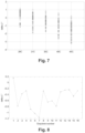
- Figure 2 is a photomicrograph illustrating edge artifacts observed after driving a block of pixels to black, followed by driving the same block of pixels to white, with use of a BPPWWTDS on the neighboring pixels.
- Figure 3 illustrates white state lightness as function of the number of updates using a prior art BPPWWTDS.
- Figure 4 is a voltage against time curve for a BPPTOPWWTDS waveform for white-to-white transitions.
- Figure 5 is a photomicrograph similar to that of Figure 2 but using a BPPTOPWWTDS of the present invention.
- Figure 6 is a graph similar to that of Figure 3 but showing the results obtained using both a prior art BPPWWTDS and a BPPTOPWWTDS of the present invention.
- Figure 7 is a graph showing the white state lightness variation obtained after 24 updates from an initial white state lightness level as a function of the number of updates using various BPPTOPWWTDS of the present invention.
- Figure 8 is a graph showing the gray levels obtained after more than 50,000 updates using a BPPTOPWWTDS of the present invention.
- Figure 9A shows a portion of a text image on a display.
- Figure 9A illustrates the effect of overlaying a menu over the text image of Figure 9A .
- Figure 9C illustrates the image resulting from subsequent removal of the menu shown in Figure 9B .
- Figure 10A shows a text image on a display.
- Figure 10B illustrates the effect of overlaying an icon over the text image of Figure 10A .
- Figure 10C illustrates the image resulting from subsequent removal of the icon shown in Figure 10B .
- Figures 11A-11C are enlarged versions of portions of Figures 10A-10C respectively illustrating the areas surrounding the icon.
- Figures 12A-12C show masks used in applying the overlay method of the present invention to the transitions shown in Figures 11A-11C respectively.
- Figure 13 is a graph of white state reflectance against time for a white pixels and shows typical white state drift in a background pixel, a problem which may be reduced or eliminated by the drift compensation method of the present invention.
- Figure 14 shows an image on a display affected by ghosting effects caused by white state drift such as that shown in Figure 13 .
- Figure 15 shows a waveform suitable for use in the drift compensation method of the present invention.
- Figures 16A and 16B are pixels maps showing areas of background pixels to which one step of the drift compensation method is to be applied, with Figure 16A showing application of the step to 12.5 per cent, and Figure 16B showing app of the step to 100 per cent, of the background pixels in the illustrated area.
- Figure 17 is a flow diagram showing the implementation of a preferred drift compensation method of the present invention.
- Figure 18 is a graph similar to that of Figure 13 but showing, in addition to the curve for an uncorrected pixel, curves for two different methods of drift compensation in accordance with the present invention.
- Figures 19A and 19B are images similar to that of Figure 14 , with Figure 19A being an uncorrected image and Figure 19B being an image corrected by a drift compensation method of the invention.
- Figure 20 is a graph similar to that of Figure 18 and again showing curves for both uncorrected and corrected pixels.
- Figure 21 is a graph of remnant voltage against time (expressed as number of cycles) for both uncorrected pixels and pixels corrected using a drift compensation method of the invention.
- the present invention provides a number of improvements in the driving of electro-optic displays, especially bistable electro-optic displays, and most especially electrophoretic displays, and in displays and components thereof arranged to carry out the improved method.
- the various improvements provided by the present invention will primarily be described separately below but it should be noted that a single physical display or component thereof may implement more than one of the improvements provided by the present invention.
- the drift compensation method of the present invention may be implemented in the same physical display as any of the other methods of the present invention.
- the update buffer aspect of the present invention provides display controllers and methods for operating a display with the T and F transitions already discussed.
- this aspect provides a display controller having an update buffer, means for removing from the update buffer pixels which do not require updating during a given transition, means for receiving a list of states that should not be removed from the update buffer, and means to ensure that pixels having listed states are not removed from the update buffer.
- states 1-16 correspond to the normal 16 gray levels
- state 17 denotes a T transition and state 18 an F transition.
- the numbers 17 and 18 are sent to the controller. If the controller algorithm recognizes a zero transition where the initial and final states are equal but on the list, the relevant pixel is not removed from the update buffer.
- Another aspect of the update buffer invention provides a display controller having an update buffer, and means for removing from the update buffer pixels which do not require updating during a given transition, the controller having at least one special transition having two states associated therewith, means to determine when a pixel is undergoing a special transition immediately after a previous special transition, and means to insert into the update buffer the second state associated with the at least one special transition when a pixel is undergoing a special transition immediately after a previous special transition.
- states 1-16 correspond to the normal 16 gray levels
- states 17 and 19 denote a T transition and state 18 and 20 an F transition.
- the controller then operates such that if, at any specific pixel, the previous transition was a T-transition, and the next transition is also a T-transition, then the state substituted into the image should be the second state associated with the T transition, namely 19. Thus, the pixel was assigned state 17 for the previous transition but is assigned state 19 for the next transition. In this way the controller will always see special transitions as a change in state the associated pixels will never be flagged and removed from the update pipeline.
- the update buffer invention also provides a modified algorithm for carrying out the SGU, BPPWWTDS or WWTOPDS drive schemes discussed above to take into account the non-flashing pixels that will be introduced by the partial update mode of the controller.
- the Partial Update Mask (PUM) value for each pixel must be computed according to the known controller algorithm. In the simplest case (standard partial update) the PUM is set to False if and only if the initial and final gray levels in the image buffer are the same.
- a modified algorithm is used which utilizes the PUM to determine local activity as prescribed by the algorithm. Pseudo-code for two such algorithms is provided below:
- a preferred regional update area for an overlaid item is the area of the item plus one pixel all around its periphery; in this one-pixel border area, the special transition for edge ghosting reduction will be applied when the overlaid item is removed.
- One controller solution involves the following sequence of actions based on a new controller functionality: creating a full screen image combining the initial image with the addition of the item ⁇ performing full screen image processing using that image and the previous initial image based on waveform algorithm ⁇ make the decision to perform a regional update using the processed new image for the area and location of the item plus one pixel all around.
- the update buffer controllers and methods of the present invention provide a pathway to use the edge and areal ghosting artifact reducing waveform techniques described in the aforementioned US 2013/0194250 on controllers that implement a "partial update" mode.
- the present invention requires only a small modification of the definition of the waveform states and a modification of the algorithm, without any changes to controller functionality.
- Part B BPPTOPWWTDS Invention
- the BPPTOPWWTDS aspect of the present invention provides a balanced pulse pair/top-off pulse white/white transition drive scheme in which pixels undergoing white-to-white transitions, identified as likely to give rise to edge artifacts, and in a spatio-temporal configuration such that the drive scheme will be efficacious in erasing or reducing the edge artifact, are driven using a waveform which comprises at least one balanced pulse pair and at least one top-off pulse.
- FIG. 4 A preferred white-to-white waveform for a BPPTOPWWTDS of the present invention is illustrated in Figure 4 of the accompanying drawings.
- the waveform comprises an initial top-off pulse in the form of a single negative (white-going) frame, followed by two frame of zero voltage, and four successive balanced pulse pairs, each of which comprises a positive (black-going) frame followed immediately by a negative (white-going) one.
- the performance of non-flashy drive schemes aimed at maintaining the background white state lightness level can be significantly improved with observed decrease in white state lightness level of less than 0.5 L ⁇ using a BPPTOPWWTDS of the present invention versus over 3L ⁇ using a prior art BPPWWTDS after 24 updates at 45°C as shown in Figure 6 .
- Preferred embodiments of a BPPTOPWWTDS of the present invention using only a single top-off pulse, but varying the number of balanced pulse pairs and the location of the top-off pulse relative to the balanced pulse pairs, have been observed to provide a wide range of possible waveform solutions for operating at from 28°C to 45°C, as illustrated in Figure 7 .
- acceptable solutions correspond to those resulting in zero delta L ⁇ after 24 updates in special low flash mode using the BPPTOPWWTDS.
- the most significant tuning elements are the location of the top-off pulse relative to the BPP's and the number of BPP's, with a small degree of tunability provided by the location of the BPP's.
- Locating the top-off pulse closer to the BPP's results in more positive delta L ⁇ solutions, with the optimal location being the frame right after the BPPs.
- the optimal location being the frame right after the BPPs.
- BPPTOPWWTDS white-to-white waveform it has been observed that decreasing the temperature results in more positive delta L ⁇ .
- a potential problem could be that the BPPTOPWWTDS could create solutions with too positive a delta L ⁇ (meaning that the display becomes whiter and whiter in an uncontrolled manner), it has been possible to avoid this problem by simply increasing the number of BPP's in the white-to-white waveform which results in a less positive delta L ⁇ .
- Figure 7 shows that the BPPTOPWWTDS of the present invention can provide good results over the temperature range of 28°C to 45°C, while still allowing enough tunability to account for module variability experienced in commercial mass production of electrophoretic displays.
- top-off pulse in the BPPTOPWWTDS of the present invention renders the drive scheme somewhat DC imbalanced, and (as discussed in several of the aforementioned MEDEOD applications), DC imbalanced drive schemes are known to potentially cause significant display reliability issues and significant changes in drive scheme performance.
- significant reduction in edge artifacts in electrophoretic displays can be achieved using just one top-off pulse in the BPPTOPWWTDS white-to-white waveform, resulting (typically) in a mild DC imbalance of just one white-going frame.
- Usage reliability experiments using a special low flash mode that make use of such a BPPTOPWWTDS have been conducted, and the results are shown in Figure 8 .
- the BPPTOPWWTDS of the present invention can significantly extend the temperature range over which electrophoretic displays can operate without producing image defects, be enabling such displays to operate for a large number of updates at the temperature range of about 30 to 45°C without being subject to the type of image defects to which prior art displays are subject, thus rendering displays using the drive scheme more attractive to users.
- the overlay aspect of the present invention provides a method for overlaying an item (an icon, menu, etc.) over existing text or image content followed by a removal of the item, and differs from standard partial updates drive schemes in that only the pixels in the region of the item perform transitions (including self transitions) in order to avoid text thinning/fading for text that overlaps with the item and to avoid seeing the text outside that area flashing on to itself.
- a regional update is performed in the area of the overlaid item.
- Preferred variants of the overlay method can allow for transparent areas within the overlaid item.
- the five-bit drive scheme solution described above cannot be applied to all 16 gray levels because a five-bit drive scheme does not provide enough additional states.
- the five-bit drive scheme solution may be applied only to a restricted number of gray levels. For example, if the algorithm requires two special states then two gray levels must be dropped from the algorithm, so that, for example, the algorithm might be applied to gray levels 1 ⁇ 14 only. Such a variant of the overlay method could still be effective is reducing text thinning/fading since most of the gray levels in text are with gray levels 1 ⁇ 14. However, in some other scenarios, restricting the process to certain gray levels might not work well enough.
- a "controller-spoofing" method can be used in conjunction with the algorithm described above.
- all the pixels requiring empty self transitions as determined by a mask are set to one same special empty state with empty self transition (for example state 2).
- That processed image is then sent to the controller using a special mode that has a fully empty waveform in order to set the states inside the controller as desired by the algorithm without actually updating the pixels of the display.
- the second image is then displayed with the use of the special empty state 2.
- a device controller function which accepts the mask described above and places pixels on the update buffer according to this mask instead of the partial update logic that it would normally perform.
- This approach is the need for a mask of the opaque part of the overlaid item. This, however, is not an unrealistic requirement since the rendering engine for the graphic user interface of a electro-optic display must have such a mask available to it, but the use of such a mask does require a greater amount of data handling and increases system complexity.
- An alternative to this mask-based approach is to determine the list of pixels with self-transitions that should be refreshed based on the activity of neighboring pixels, i.e., the mask is inferred from the image data, and subsequent steps implement the approach as if it were mask-based.
- one algorithm may be defined as: For a given pixel with a given gray level in the current image:
- Such an algorithm should be applied in a non-recursive manner in order to avoid a propagation effect, i.e., setting a pixel to perform a non-empty self transition as determined from this algorithm would not trigger setting its cardinal neighbors with self transitions to perform non-empty self transitions. For example, if a feature contains several columns of pixels that are performing self transitions in an image sequence while an icon is being overlaid and dismissed multiple times on top of that feature, this algorithm would trigger the columns of pixels at the edge of the feature to perform non-empty self transitions. Such an approach should result in reducing most of the visible text thinning/fading as blooming typically affects only the immediate cardinal neighbors.
- the algorithm described above is general in the sense that it is applied to all gray levels, including white, and thus in a partial update mode in which the background white state is not intended to flash, some white pixels in the background may perform white ⁇ white transitions depending on the activity of their neighboring pixels. For example, if a long black line is written on the display, all the neighboring pixels around the black line would perform white ⁇ white transitions, resulting in lines and geometric features with uniform thicknesses, thus avoiding the issue of non-uniform line thickness which has plagued prior art partial update drive schemes. However, the pixels performing white ⁇ white transitions may induce the formation of edge artifacts around them.
- Such a drive method would be applied in conjunction with a display mode designed to reduce edge artifacts in order to avoid the formation of those artifacts.
- Another variation of this method would except certain gray levels; for example, the method could be applied to all gray levels except white, thus avoiding the aforementioned edge artifact problem.
- a five-bit drive scheme may be used if only 16 gray levels are required. If additional special states exist in the drive scheme, the method may be applied to most but not all of the gray levels, for example gray levels 1 ⁇ 14 of 16. As with the mask-based approach, this drive scheme would solve most of the text thinning/fading issues. If it is necessary to apply the method to all existing states, then the implementation of this method would require resetting the states inside the controller as described previously with the use of two additional empty display updates.
- the method of the present invention can reduce or eliminate problems such as text thinning and fading encountered in prior art partial update drive schemes, while maintaining the low-flash characteristics of a partial update drive scheme for electro-optic displays.
- the present method is compatible with novel drive scheme algorithms that result in low-flash, high image quality display performance, thus rendering displays using the drive scheme very attractive to users.
- Part D Drift Compensation Invention
- the drift compensation aspect of the invention provides a method of driving a bistable electro-optic display having a plurality of pixels each capable of displaying two extreme optical states, in which, after the display has been left undriven for a period of time, successive refresh pulses are applied to proportions of the background pixels to reverse at least partially the effects of drift.
- the drift compensation method may be regarded as a combination of a specially designed waveform with an algorithm and (desirably) a timer to actively compensate for the background white state (or other ) drift as seen in some electro-optic and especially electrophoretic displays.
- the special waveform is applied to selected pixels in the background white state when a triggering event occurs that is typically based on a timer in order to drive the white state reflectance up slightly in a controlled manner.
- FIG. 15 One example of a waveform useful in the drift compensation method is shown in Figure 15 .
- This waveform may be as short as 2 frames (about 24 milliseconds with a typical 85Hz frame rate) and may contain a single white-going top-off pulse (frame 1).
- the purpose of this waveform is to slightly increase the background white state in a way that is essentially invisible to the user and therefore non-intrusive.
- the drive voltage of the top-off pulse may be modulated (for example -10V instead of the -15V used in other transitions) in order to control the amount of white state increase.
- the waveform of Figure 15 or a similar waveform is applied to selected pixels in the background white state, thus allowing a control white state increase from the update, as illustrated in Figures 16A and 16B .
- PMM pixel map matrix
- the algorithm used may be a simplified version of the algorithm described in the aforementioned US 2013/0194250 .
- the special transition shown in Figure 15 would correspond to the F W ⁇ W transition discussed in this published application.
- Drift compensation is applied by requesting a special update to the image currently displayed on the display.
- the special update calls a separate mode storing a waveform that is empty for all transitions, except for the special transition shown in Figure 15 .
- the waveform algorithm will select the pixels that will receive the top-off pulse using the waveform algorithm described below.
- PMM_VS, PMM_HS, PMM Period are the vertical size, horizontal size, and period of the pixel map matrix.
- An update counter ensures that all the pixels will uniformly receive the same amount of top-off pulses over time.
- a typical algorithm is as follows:
- the drift compensation method very desirable incorporates the use of a timer.
- the special waveform used results in an increase in the background white state lightness. Therefore, if this update was tied to user-requested updates, there would be large variations in white state increase depending on how quickly updates were being requested, i.e., if this special update were applied every time a user requested an update, the white state increase would become unacceptably high if a user turned pages very quickly (such as every one second), as opposed to a user turning pages more slowly (such as every thirty seconds). This would result in the drift compensation method being very sensitive to dwell times between updates and in some cases unacceptably high ghosting would occur due to the background white state being increased too much.
- the use of a timer decouples drift compensation from user-requested updates. By applying the special update independently of user-requested updates, the drift compensation is more controlled and less sensitive to dwell times.
- a timer may be used in the drift compensation method in several ways.
- a timeout value or timer period may function as an algorithm parameter; each time the timer reaches the timeout value or a multiple of the timer period, it triggers an event that requests the special update described above and resets the timer in the case of the timeout value.
- the timer may be reset when a full screen refresh (a global complete update) is requested.
- the timeout value or timer period may vary with temperature in order to accommodate the variation of drift with temperature.
- An algorithm flag may be provided to prevent drift compensation being applied at temperatures at which it is not necessary.
- Figure 17 is a flow diagram of a drift compensation method implementing the concepts discussed in this paragraph.
- Other variations may include using the timer information in conjunction with the time since the last user-requested page turn. For example, if the user has not requested page turns for some time, application of top-off pulses may cease after a predetermined maximum time. Alternatively, the top-off pulse could be combined with a user-requested update.
- FIG 18 Examples of the background white state over time with and without drift compensation are shown in Figure 18 .
- the lowest curve (similar to that shown in Figure 13 ) shows the uncorrected background white state over the course of 45 page turns at 30 second intervals. The illustrated drop in white state reflectance would result in substantial text ghosting over time.
- the center curve shows the result of drift compensation in which 12.5% of the pixels receive the special update every minute, again while 45 page turns occur at 30 second intervals.
- the upper curve shows a second example of drift compensation in which 100% of the pixels receive the special update every six minutes, using the same sequence of page turns.
- the background white state is maintained at a higher level over time which will result in reduced text ghosting and may allow to achieving a higher number of page turns without a full display refresh.
- the white state drift correction may be tuned by a combination of the pixel map matrix, the timer period, and the drive voltage for the top-off pulse.
- Figure 20 illustrates the tuning of the background white state drift by varying the density of the pixel map matrix from 12.5% to 50% with a fixed timer of three minutes, using the same sequence of page turns as in Figure 18 .
- Figure 21 shows curves of remnant voltage against time for an uncorrected pixel and three pixels using different drift compensation methods for the same sequence of page turns as in Figure 20 .
- Figure 21 shows that in the worst case, drift compensation results in an increase of remnant voltage of about 100mV above the baseline.
- Prior knowledge indicates that remnant voltages within a window of about ⁇ 250mV are typical in normal usage. Therefore, Figure 21 indicates that drift compensation does not appear to have a significant impact on the remnant voltage, and therefore on display reliability with usage.
- drift compensation can be applied to dark state drift as well as white state drift.
- a typical waveform for dark state drift compensation could be simply the inverse of that shown in Figure 15 , with a single frame of positive voltage.
- the drift compensation method of the present invention provides a means for substantially reducing the effects of drift on a displayed image in a manner which is typically unnoticeable to a user and which does not adversely affect the long term use of the display.
- the methods of the present invention may be "tuned" to produce accurate gray levels using any of the techniques described in the aforementioned MEDEOD applications.
- the waveform used may include drive pulses having a polarity opposite to that of the waveform as a whole.
- the waveform will typically have an overall black-going polarity.
- At least one balanced pulse pair (a pair of drive pulses of substantially equal absolute impulse value, but of opposite polarity) and/or at least one period of zero voltage in the waveform.
Abstract
Description
- This application is related to
U.S. Patents Nos. 5,930,026 ;6,445,489 ;6,504,524 ;6,512,354 ;6,531,997 ;6,753,999 ;6,825,970 ;6,900,851 ;6,995,550 ;7,012,600 ;7,023,420 ;7,034,783 ;7,116,466 ;7,119,772 ;7,193,625 ;7,202,847 ;7,259,744 ;7,304,787 ;7,312,794 ;7,327,511 ;7,453,445 ;7,492,339 ;7,528,822 ;7,545,358 ;7,583,251 ;7,602,374 ;7,612,760 ;7,679,599 ;7,688,297 ;7,729,039 ;7,733,311 ;7,733,335 ;7,787,169 ;7,952,557 ;7,956,841 ;7,999,787 ; and8,077,141 ; andU.S. Patent Applications Publication Nos. 2003/0102858 ;2005/0122284 ;2005/0179642 ;2005/0253777 ;2006/0139308 ;2007/0013683 ;2007/0091418 ;2007/0103427 ;2007/0200874 ;2008/0024429 ;2008/0024482 ;2008/0048969 ;2008/0129667 ;2008/0136774 ;2008/0150888 ;2008/0291129 ;2009/0174651 ;2009/0179923 ;2009/0195568 ;2009/0256799 ;2009/0322721 ;2010/0045592 ;2010/0220121 ;2010/0220122 ;2010/0265561 2011/0285754 , and2013/0194250 . - The aforementioned patents and applications may hereinafter for convenience collectively be referred to as the "MEDEOD" (MEthods for Driving Electro-Optic Displays) applications. The entire contents of these patents and copending applications, and of all other U.S. patents and published and copending applications mentioned below, are herein incorporated by reference.
- The background nomenclature and state of the art regarding electro-optic displays is discussed at length in
U.S. Patent No. 7,012,600 to which the reader is referred for further information. Accordingly, this nomenclature and state of the art will be briefly summarized below. - The present invention relates to methods for driving electro-optic displays, especially bistable electro-optic displays, and to apparatus for use in such methods. More specifically, this invention relates to driving methods which may allow for reduced "ghosting" and edge effects, and reduced flashing in such displays. This invention is especially, but not exclusively, intended for use with particle-based electrophoretic displays in which one or more types of electrically charged particles are present in a fluid and are moved through the fluid under the influence of an electric field to change the appearance of the display.
- The term "electro-optic", as applied to a material or a display, is used herein in its conventional meaning in the imaging art to refer to a material having first and second display states differing in at least one optical property, the material being changed from its first to its second display state by application of an electric field to the material. Although the optical property is typically color perceptible to the human eye, it may be another optical property, such as optical transmission, reflectance, luminescence or, in the case of displays intended for machine reading, pseudo-color in the sense of a change in reflectance of electromagnetic wavelengths outside the visible range.
- The term "gray state" is used herein in its conventional meaning in the imaging art to refer to a state intermediate two extreme optical states of a pixel, and does not necessarily imply a black-white transition between these two extreme states. For example, several of the E Ink patents and published applications referred to below describe electrophoretic displays in which the extreme states are white and deep blue, so that an intermediate "gray state" would actually be pale blue. Indeed, as already mentioned, the change in optical state may not be a color change at all. The terms "black" and "white" may be used hereinafter to refer to the two extreme optical states of a display, and should be understood as normally including extreme optical states which are not strictly black and white, for example the aforementioned white and dark blue states. The term "monochrome" may be used hereinafter to denote a drive scheme which only drives pixels to their two extreme optical states with no intervening gray states.
- The terms "bistable" and "bistability" are used herein in their conventional meaning in the art to refer to displays comprising display elements having first and second display states differing in at least one optical property, and such that after any given element has been driven, by means of an addressing pulse of finite duration, to assume either its first or second display state, after the addressing pulse has terminated, that state will persist for at least several times, for example at least four times, the minimum duration of the addressing pulse required to change the state of the display element. It is shown in
U.S. Patent No. 7,170,670 that some particle-based electrophoretic displays capable of gray scale are stable not only in their extreme black and white states but also in their intermediate gray states, and the same is true of some other types of electro-optic displays. This type of display is properly called "multi-stable" rather than bistable, although for convenience the term "bistable" may be used herein to cover both bistable and multi-stable displays. - The term "impulse" is used herein in its conventional meaning of the integral of voltage with respect to time. However, some bistable electro-optic media act as charge transducers, and with such media an alternative definition of impulse, namely the integral of current over time (which is equal to the total charge applied) may be used. The appropriate definition of impulse should be used, depending on whether the medium acts as a voltage-time impulse transducer or a charge impulse transducer.
- Much of the discussion below will focus on methods for driving one or more pixels of an electro-optic display through a transition from an initial gray level to a final gray level (which may or may not be different from the initial gray level). The term "waveform" will be used to denote the entire voltage against time curve used to effect the transition from one specific initial gray level to a specific final gray level. Typically such a waveform will comprise a plurality of waveform elements; where these elements are essentially rectangular (i.e., where a given element comprises application of a constant voltage for a period of time); the elements may be called "pulses" or "drive pulses". The term "drive scheme" denotes a set of waveforms sufficient to effect all possible transitions between gray levels for a specific display. A display may make use of more than one drive scheme; for example, the aforementioned
U. S. Patent No. 7,012,600 teaches that a drive scheme may need to be modified depending upon parameters such as the temperature of the display or the time for which it has been in operation during its lifetime, and thus a display may be provided with a plurality of different drive schemes to be used at differing temperature etc. A set of drive schemes used in this manner may be referred to as "a set of related drive schemes." It is also possible, as described in several of the aforementioned MEDEOD applications, to use more than one drive scheme simultaneously in different areas of the same display, and a set of drive schemes used in this manner may be referred to as "a set of simultaneous drive schemes." - Several types of electro-optic displays are known, for example:
- (a) rotating bichromal member displays (see, for example,
U.S. Patents Nos. 5,808,783 ;5,777,782 ;5,760,761 ;6,054,071 6,055,091 ;6,097,531 ;6,128,124 ;6,137,467 ; and6,147,791 ); - (b) electrochromic displays (see, for example, O'Regan, B., et al., Nature 1991, 353, 737; Wood, D., Information Display, 18(3), 24 (March 2002); Bach, U., et al., Adv. Mater., 2002, 14(11), 845; and
U.S. Patents Nos. 6,301,038 ;6,870.657 ; and6,950,220 ); - (c) electro-wetting displays (see Hayes, R.A., et al., "Video-Speed Electronic Paper Based on Electrowetting", Nature, 425, 383-385 (25 September 2003) and
U.S. Patent Publication No. 2005/0151709 ); - (d) particle-based electrophoretic displays, in which a plurality of charged particles move through a fluid under the influence of an electric field (see
U.S. Patents Nos. 5,930,026 ;5,961,804 ;6,017,584 ;6,067,185 ;6,118,426 ;6,120,588 ;6,120,839 ;6,124,851 ;6,130,773 ; and6,130,774 ;U.S. Patent Applications Publication Nos. 2002/0060321 ;2002/0090980 ;2003/0011560 ;2003/0102858 ;2003/0151702 ;2003/0222315 ;2004/0014265 ;2004/0075634 ;2004/0094422 ;2004/0105036 ;2005/0062714 ; and2005/0270261 ; and International Applications Publication Nos.WO 00/38000 WO 00/36560 WO 00/67110 WO 01/07961 European Patents Nos. 1,099,207 B1 ; and1,145,072 B1 ; and the other MIT and E Ink patents and applications discussed in the aforementionedU.S. Patent No. 7,012,600 ). - There are several different variants of electrophoretic media. Electrophoretic media can use liquid or gaseous fluids; for gaseous fluids see, for example, Kitamura, T., et al., "Electrical toner movement for electronic paper-like display", IDW Japan, 2001, Paper HCS1-1, and Yamaguchi, Y., et al., "Toner display using insulative particles charged triboelectrically", IDW Japan, 2001, Paper AMD4-4);
U.S. Patent Publication No. 2005/0001810 ;European Patent Applications 1,462,847 ;1,482,354 ;1,484,635 ;1,500,971 ;1,501,194 ;1,536,271 ;1,542,067 ;1,577,702 ;1,577,703 ; and1,598,694 ; andInternational Applications WO 2004/090626 ;WO 2004/079442 ; andWO 2004/001498 . The media may be encapsulated, comprising numerous small capsules, each of which itself comprises an internal phase containing electrophoretically-mobile particles suspended in a liquid suspending medium, and a capsule wall surrounding the internal phase. Typically, the capsules are themselves held within a polymeric binder to form a coherent layer positioned between two electrodes; see the aforementioned MIT and E Ink patents and applications. Alternatively, the walls surrounding the discrete microcapsules in an encapsulated electrophoretic medium may be replaced by a continuous phase, thus producing a so-called polymer-dispersed electrophoretic display, in which the electrophoretic medium comprises a plurality of discrete droplets of an electrophoretic fluid and a continuous phase of a polymeric material; see for example,U.S. Patent No. 6,866,760 . For purposes of the present application, such polymer-dispersed electrophoretic media are regarded as sub-species of encapsulated electrophoretic media. Another variant is a so-called "microcell electrophoretic display" in which the charged particles and the fluid are retained within a plurality of cavities formed within a carrier medium, typically a polymeric film; see, for example,U.S. Patents Nos. 6,672,921 and6,788,449 . - An encapsulated electrophoretic display typically does not suffer from the clustering and settling failure mode of traditional electrophoretic devices and provides further advantages, such as the ability to print or coat the display on a wide variety of flexible and rigid substrates. (Use of the word "printing" is intended to include all forms of printing and coating, including, but without limitation: pre-metered coatings such as patch die coating, slot or extrusion coating, slide or cascade coating, curtain coating; roll coating such as knife over roll coating, forward and reverse roll coating; gravure coating; dip coating; spray coating; meniscus coating; spin coating; brush coating; air knife coating; silk screen printing processes; electrostatic printing processes; thermal printing processes; ink jet printing processes; electrophoretic deposition (See
U.S. Patent No. 7,339,715 ); and other similar techniques.) Thus, the resulting display can be flexible. Further, because the display medium can be printed (using a variety of methods), the display itself can be made inexpensively. - Other types of electro-optic media may also be used in the displays of the present invention.
- The bistable or multi-stable behavior of particle-based electrophoretic displays, and other electro-optic displays displaying similar behavior (such displays may hereinafter for convenience be referred to as "impulse driven displays"), is in marked contrast to that of conventional liquid crystal ("LC") displays. Twisted nematic liquid crystals are not bi- or multi-stable but act as voltage transducers, so that applying a given electric field to a pixel of such a display produces a specific gray level at the pixel, regardless of the gray level previously present at the pixel. Furthermore, LC displays are only driven in one direction (from non-transmissive or "dark" to transmissive or "light"), the reverse transition from a lighter state to a darker one being effected by reducing or eliminating the electric field. Finally, the gray level of a pixel of an LC display is not sensitive to the polarity of the electric field, only to its magnitude, and indeed for technical reasons commercial LC displays usually reverse the polarity of the driving field at frequent intervals. In contrast, bistable electro-optic displays act, to a first approximation, as impulse transducers, so that the final state of a pixel depends not only upon the electric field applied and the time for which this field is applied, but also upon the state of the pixel prior to the application of the electric field.
- Whether or not the electro-optic medium used is bistable, to obtain a high-resolution display, individual pixels of a display must be addressable without interference from adjacent pixels. One way to achieve this objective is to provide an array of non-linear elements, such as transistors or diodes, with at least one non-linear element associated with each pixel, to produce an "active matrix" display. An addressing or pixel electrode, which addresses one pixel, is connected to an appropriate voltage source through the associated non-linear element. Typically, when the non-linear element is a transistor, the pixel electrode is connected to the drain of the transistor, and this arrangement will be assumed in the following description, although it is essentially arbitrary and the pixel electrode could be connected to the source of the transistor. Conventionally, in high resolution arrays, the pixels are arranged in a two-dimensional array of rows and columns, such that any specific pixel is uniquely defined by the intersection of one specified row and one specified column. The sources of all the transistors in each column are connected to a single column electrode, while the gates of all the transistors in each row are connected to a single row electrode; again the assignment of sources to rows and gates to columns is conventional but essentially arbitrary, and could be reversed if desired. The row electrodes are connected to a row driver, which essentially ensures that at any given moment only one row is selected, i.e., that there is applied to the selected row electrode a voltage such as to ensure that all the transistors in the selected row are conductive, while there is applied to all other rows a voltage such as to ensure that all the transistors in these non-selected rows remain non-conductive. The column electrodes are connected to column drivers, which place upon the various column electrodes voltages selected to drive the pixels in the selected row to their desired optical states. (The aforementioned voltages are relative to a common front electrode which is conventionally provided on the opposed side of the electro-optic medium from the non-linear array and extends across the whole display.) After a pre-selected interval known as the "line address time" the selected row is deselected, the next row is selected, and the voltages on the column drivers are changed so that the next line of the display is written. This process is repeated so that the entire display is written in a row-by-row manner.
- It might at first appear that the ideal method for addressing such an impulse-driven electro-optic display would be so-called "general grayscale image flow" in which a controller arranges each writing of an image so that each pixel transitions directly from its initial gray level to its final gray level. However, inevitably there is some error in writing images on an impulse-driven display. Some such errors encountered in practice include:
- (a) Prior State Dependence; With at least some electro-optic media, the impulse required to switch a pixel to a new optical state depends not only on the current and desired optical state, but also on the previous optical states of the pixel.
- (b) Dwell Time Dependence; With at least some electro-optic media, the impulse required to switch a pixel to a new optical state depends on the time that the pixel has spent in its various optical states. The precise nature of this dependence is not well understood, but in general, more impulse is required the longer the pixel has been in its current optical state.
- (c) Temperature Dependence; The impulse required to switch a pixel to a new optical state depends heavily on temperature.
- (d) Humidity Dependence; The impulse required to switch a pixel to a new optical state depends, with at least some types of electro-optic media, on the ambient humidity.
- (e) Mechanical Uniformity; The impulse required to switch a pixel to a new optical state may be affected by mechanical variations in the display, for example variations in the thickness of an electro-optic medium or an associated lamination adhesive. Other types of mechanical non-uniformity may arise from inevitable variations between different manufacturing batches of medium, manufacturing tolerances and materials variations.
- (f) Voltage Errors; The actual impulse applied to a pixel will inevitably differ slightly from that theoretically applied because of unavoidable slight errors in the voltages delivered by drivers.
- Thus, general grayscale image flow requires very precise control of applied impulse to give good results, and empirically it has been found that, in the present state of the technology of electro-optic displays, general grayscale image flow is infeasible in a commercial display.
- Under some circumstances, it may be desirable for a single display to make use of multiple drive schemes. For example, a display capable of more than two gray levels may make use of a gray scale drive scheme ("GSDS") which can effect transitions between all possible gray levels, and a monochrome drive scheme ("MDS") which effects transitions only between two gray levels, the MDS providing quicker rewriting of the display that the GSDS. The MDS is used when all the pixels which are being changed during a rewriting of the display are effecting transitions only between the two gray levels used by the MDS. For example, the aforementioned
U.S. Patent No. 7,119,772 describes a display in the form of an electronic book or similar device capable of displaying gray scale images and also capable of displaying a monochrome dialogue box which permits a user to enter text relating to the displayed images. When the user is entering text, a rapid MDS is used for quick updating of the dialogue box, thus providing the user with rapid confirmation of the text being entered. On the other hand, when the entire gray scale image shown on the display is being changed, a slower GSDS is used. - Alternatively, a display may make use of a GSDS simultaneously with a "direct update" drive scheme ("DUDS"). The DUDS may have two or more than two gray levels, typically fewer than the GSDS, but the most important characteristic of a DUDS is that transitions are handled by a simple unidirectional drive from the initial gray level to the final gray level, as opposed to the "indirect" transitions often used in a GSDS, where in at least some transitions the pixel is driven from an initial gray level to one extreme optical state, then in the reverse direction to a final gray level (this type of waveform may for convenience be referred to as a "single rail bounce" waveform); in some cases, the transition may be effected by driving from the initial gray level to one extreme optical state, thence to the opposed extreme optical state, and only then to the final extreme optical state (this type of waveform may for convenience be referred to as a "double rail bounce" waveform) - see, for example, the drive scheme illustrated in
Figures 11A and 11B of the aforementionedU. S. Patent No. 7,012,600 . Present electrophoretic displays may have an update time in grayscale mode of about two to three times the length of a saturation pulse (where "the length of a saturation pulse" is defined as the time period, at a specific voltage, that suffices to drive a pixel of a display from one extreme optical state to the other), or approximately 700-900 milliseconds, whereas a DUDS has a maximum update time equal to the length of the saturation pulse, or about 200-300 milliseconds. - Variation in drive schemes is, however, not confined to differences in the number of gray levels used. For example, drive schemes may be divided into global drive schemes, where a drive voltage is applied to every pixel in the region to which the global update drive scheme (more accurately referred to as a "global complete" or "GC" drive scheme) is being applied (which may be the whole display or some defined portion thereof) and partial update drive schemes, where a drive voltage is applied only to pixels that are undergoing a non-zero transition (i.e., a transition in which the initial and final gray levels differ from each other), but no drive voltage is applied during zero transitions (in which the initial and final gray levels are the same). An intermediate form a drive scheme (designated a "global limited" or "GL" drive scheme) is similar to a GC drive scheme except that no drive voltage is applied to a pixel which is undergoing a zero, white-to-white transition. In, for example, a display used as an electronic book reader, displaying black text on a white background, there are numerous white pixels, especially in the margins and between lines of text which remain unchanged from one page of text to the next; hence, not rewriting these white pixels substantially reduces the apparent "flashiness" of the display rewriting. However, certain problems remain in this type of GL drive scheme. Firstly, as discussed in detail in some of the aforementioned MEDEOD applications, bistable electro-optic media are typically not completely bistable, and pixels placed in one extreme optical state gradually drift, over a period of minutes to hours, towards an intermediate gray level. In particular, pixels driven white slowly drift towards a light gray color. Hence, if in a GL drive scheme a white pixel is allowed to remain undriven through a number of page turns, during which other white pixels (for example, those forming parts of the text characters) are driven, the freshly updated white pixels will be slightly lighter than the undriven white pixels, and eventually the difference will become apparent even to an untrained user.
- Secondly, when an undriven pixel lies adjacent a pixel which is being updated, a phenomenon known as "blooming" occurs, in which the driving of the driven pixel causes a change in optical state over an area slightly larger than that of the driven pixel, and this area intrudes into the area of adjacent pixels. Such blooming manifests itself as edge effects along the edges where the undriven pixels lie adjacent driven pixels. Similar edge effects occur when using regional updates (where only a particular region of the display is updated, for example to show an image), except that with regional updates the edge effects occur at the boundary of the region being updated. Over time, such edge effects become visually distracting and must be cleared. Edge ghosting is clearly visible for example after multiple text page updates followed by an update to a white page where the contour of the previous text will appear darker compared to the background. Hitherto, such edge effects (and the effects of color drift in undriven white pixels) have typically been removed by using a single GC update at intervals. Unfortunately, use of such an occasional GC update reintroduces the problem of a "flashy" update, and indeed the flashiness of the update may be heightened by the fact that the flashy update only occurs at long intervals.
- The aforementioned
US 2013/0194250 describes techniques for reducing flashing and edge ghosting. One such technique, denoted a "selective general update" or "SGU" method, involves driving an electro-optic display having a plurality of pixels using a first drive scheme, in which all pixels are driven at each transition, and a second drive scheme, in which pixels undergoing some transitions are not driven. The first drive scheme is applied to a non-zero minor proportion of the pixels during a first update of the display, while the second drive scheme is applied to the remaining pixels during the first update. During a second update following the first update, the first drive scheme is applied to a different non-zero minor proportion of the pixels, while the second drive scheme is applied to the remaining pixels during the second update. Typically, the SGU method is applied to refreshing the white background surrounding text or an image, so that only a minor proportion of the pixels in the white background undergo updating during any one display update, but all pixels of the background are gradually updated so that drifting of the white background to a gray color is avoided without any need for a flashy update. It will readily be apparent to those skilled in the technology of electro-optic displays that application of the SGU method requires a special waveform (hereinafter referred to as an "F" waveform) for the individual pixels which are to undergo updating on each transition. - The aforementioned
US 2013/0194250 also describes a "balanced pulse pair white/white transition drive scheme" or "BPPWWTDS", which involves the application of one or more balanced pulse pairs (a balanced pulse pair or "BPP" being a pair of drive pulses of opposing polarities such that the net impulse of the balanced pulse pair is substantially zero) during white-to-white transitions in pixels which can be identified as likely to give rise to edge artifacts, and are in a spatio-temporal configuration such that the balanced pulse pair(s) will be efficacious in erasing or reducing the edge artifact. Desirably, the pixels to which the BPP is applied are selected such that the BPP is masked by other update activity. Note that application of one or more BPP's does not affect the desirable DC balance of a drive scheme since each BPP inherently has zero net impulse and thus does not alter the DC balance of a drive scheme. A second such technique, denoted "white/white top-off pulse drive scheme" or "WWTOPDS", involves applying a "top-off' pulse during white-to-white transitions in pixels which can be identified as likely to give rise to edge artifacts, and are in a spatio-temporal configuration such that the top-off pulse will be efficacious in erasing or reducing the edge artifact. Application of the BPPWWTDS or WWTOPDS again requires a special waveform (hereinafter referred to as a "T" waveform) for the individual pixels which are to undergo updating on each transition. The T and F waveforms are normally only applied to pixels undergoing white-to-white transitions. In a global limited drive scheme, the white-to-white waveform is empty (i.e., consists of a series of zero voltage pulses) whereas all other waveforms are not empty. Accordingly, when applicable the non-empty T and F waveforms replace the empty white-to-white waveforms in a global limited drive scheme. - It is necessary to distinguish between a partial update drive scheme (in which at least some zero transitions use empty waveforms) and a partial update mode of a drive controller. A partial update mode is a controller function by which, when active, a pixel is removed from the update pipeline if it is a zero transition. For example if the initial state of a pixel was
gray level 7 and the final state is alsogray level 7, then that pixel will not be assigned to a transition pipeline and will be free to participate in another subsequent update at any time. In a partial update mode, only areas in the next image buffer that differ from the current image buffer will be driven by the drive scheme. This is especially helpful when overlaying an item (such as an icon, cursor or menu over an existing image (typically text); the overlaid can be stamped into the image buffer and sent to the controller, but only the area of the overlaid item will flash. - As already indicated, partial update behavior can also be expressed by drive scheme design. For example, a global limited (GL) mode may have an empty white-to-white transition but non-empty gray-to-gray and black-to-black transitions, so a white background will not flash when overlaying a menu, but the non-white text would flash. Other waveform modes such as DU and GU have all empty zero-transitions. In this case the behavior of the display will be exactly as described for partial update mode, but with one important difference: the zero transition pixels are not removed from the pipeline and must be driven with zeros for the full duration of the update.
- One can envision a selective partial update mode in which a zero transition pixel may or may not be removed from the update pipeline (or alternatively, receive a zero transition waveform) depending on an algorithmic decision. This concept may be generalized in the following manner. Each pixel of the display has an associated flag indicating whether that pixel does or does not receive an appropriate waveform. The flags define a Partial Update Mask (PUM) for the whole image in which flags are set TRUE for pixels that are driven and FALSE for pixels which are not driven. Any pixel undergoing a non-zero transition has a TRUE flag, but pixels undergoing zero transitions may have TRUE or FALSE flags.
- Some issues arise when the aforementioned T- and F-transitions are used with partial updates. Firstly, two additional device controller states are required to enable the T- and F-transitions. For simplicity assume states 1-16 correspond to the normal 16 gray levels, while
state 17 denotes a T transition andstate 18 an F transition. A drive scheme is defined to convert any one initial state into any one final state. In one form of the method, the final image buffer is preprocessed to determine when to substitutestate - A more difficult issue is that the decisions to use T or F transitions on a pixel is based on the initial and final states of pixels adjacent to the pixel being considered; in particular, in some cases if neighboring pixels are undergoing non-zero transitions, the decision as to whether to use T or F transitions on the pixel being considered can be changed. The use of a partial update mode can thwart the ability of the algorithm to correctly identify neighboring pixels not undergoing non-zero transitions, which can lead to reduced efficacy or even the introduction of new artifacts.
- A controller may also make use of a "regional update mode"; this mode is similar to a partial update mode except that only pixels within a selected region of the display are placed on the update pipeline. A regional update mode can be considered to be a specific case of a selective partial update mode in which the Partial Update Mask is set to FALSE for any pixel outside of the selected region. However, regional updates require special handling, as described below, because typically only data for the selected region is transferred to the controller.
- A second aspect of the present invention relates to improving performance of displays at temperatures above room temperature, for example when a display in the form of an electronic book reader is being used outdoors in summer. As already mentioned,
US 2013/0194250 describes a "balanced pulse pair white/white transition drive scheme" or "BPPWWTDS". In some cases, for example some electrophoretic displays operated at temperatures of 30°C and above, a BPPWWTDS has been shown to be ineffective in reducing all edge artifacts.Figure 1 shows that using a BPPWWTDS at 31°C and 35°C results in near zero improvement in edge ghosting scores after ten iterations with the use of a BPPWWTDS as compared with use of a drive scheme lacking balanced pulse pairs. While it has been observed that a BPPWWTDS is effective in reducing edge ghosting in the area between adjacent pixels as seen inFigure 2 (which shows a photomicrograph illustrating edge artifacts observed at 45°C after ten iterations of driving a block of pixels to black, as illustrated on the left side ofFigure 2 , followed by driving the same block of pixels to white, as illustrated on the right side, with use of a BPPWWTDS on the neighboring pixels), the issue is that additional effects occurring at these temperatures result in edge artifacts that a BPPWWTDS is ineffective in reducing. For example, when a pixel is updated from white to black with inactive neighbors, one-pixel-wide edge artifacts are observed in its neighbors in the form of pixel darkening and outer edge formation which can be described as high irreversible blooming and can be explained by lateral coupling. These effects build up with the number of updates and quickly result in significant darkening in neighboring pixels. In display operation modes using a BPPWWTDS, such effects can result in significant decrease in performance. For example, in a low flash mode using a BPPWWTDS aimed at maintaining the background white state lightness level, such effects result in unacceptably high decrease in white state lightness level of over 3L∗ after 24 updates at 45°C as seen inFigure 3 . - The second aspect of the present invention relates to a DC imbalanced drive scheme intended to significantly reduce the aforementioned disadvantages of the BPPWWTDS.
- A third aspect of the invention relates to improved selective partial update drive schemes. As mentioned above, electro-optic displays can be driven using partial updates, in which all pixels with any "self-transition" (zero transition) going from one image to the next (meaning that the pixel goes from a specific gray level in one image to the same specific gray level in the subsequent image), are not driven or (which amounts to the same thing) are driven with a waveform having a voltage list of zeros. Partial updates may be performed using a special waveform in which all the self-transitions are empty, i.e. filled with zeros, (usually called a "local" waveform) or using a device command that automatically detects self-transitions (known as a "partial update mode").
- Partial updates offer benefits in terms of reduced display flashiness. For example, with an initial image that has some text, a partial update may be used if we want to overlay a menu option on top of the text in order to avoid seeing the text updating on to itself. However, partial updates can create problems and/or be undesirable and incompatible with certain drive schemes. For example, consider a menu overlying existing text that is displayed and then dismissed as illustrated in
Figures 9A-9C . If a partial update drive scheme is used, in text that overlaps with the border of the menu (as shown inFigure 9B ), all pixels with self-transition will be driven with an empty waveform, while their neighbors may be performing transitions with a non-zero waveform, e.g. a voltage list effecting a white-to-black switch from the first image to the second, followed by a black-to-white switch from the second image (Figure 9B ) to the third (Figure 9C ). These neighboring pixels may bloom over the undriven self-transition pixels, resulting in visually apparent text thinning or text fading, as illustrated in the third image. - As described in some of the aforementioned MEDEOD applications, electro-optic displays may also be driven using regional updates, in which only pixels within a selected region of the display (this region may be rectangular or of an arbitrary shape, including being selected pixel by pixel) are driven.
- The third aspect of the present invention relates to driving electro-optic displays using selective partial update drive schemes which permit retention of the benefits of partial update drive schemes in terms of reduced flashiness without creating text thinning/fading and with full compatibility with novel display modes for optimal display performance.
- A fourth aspect of the present invention relates to drift compensation, that is to say compensating for changes in the optical state of an electro-optic display with time. As already noted, electrophoretic and similar electro-optic displays are bistable. However, the bistability of such displays is not unlimited in practice, a phenomenon known as image drift occurs, whereby pixels in or near extreme optical states tend to revert very slowly to intermediate gray levels; for example, black pixels gradually become dark gray and white pixels gradually become light gray. The white state drift is of particular interest because many electro-optic displays are most commonly used to display images with a white background; for example, electronic book readers normally mimic printed books by displaying black text on a white background. If an electro-optic display is updated using a global limited drive scheme for a long periods of time without a full display refresh, the white state drift becomes an essential part of the overall visual appearance of the display. Over time, the display will show areas of the display where the white state has been recently rewritten and other areas such as the background where the white state has not recently been rewritten and has thus been drifting for some time. This results an optical artifact known as ghosting, whereby the display shows traces of previous images. Such ghosting effects are sufficiently annoying to most users that their presence a significant part in preventing the use of global limited drive schemes exclusively for long periods of time.
-
Figure 13 shows an example of how the background white state of a display may drift over the course of about twenty minutes, resulting in significant ghosting as illustrated inFigure 14 , which shows an image after turning 45 text pages in low flash mode with 30 seconds between page turns. In the last image as illustrated inFigure 14 , the text page has just been updated to a white page, and shows the ghosting resulting from "new" white in the text area versus "old" white in the background. - The fourth aspect of the present invention relates to a method for driving a display which reduces or eliminates the problems caused by drift without producing the flash which would be perceived if all background pixels were updated simultaneously as in a global complete drive scheme.
- The first aspect of the present invention (which may hereinafter be referred to as the "Update Buffer Invention") provides a display controller (capable of controlling the operation of a bistable electro-optic display) having an update buffer, means for removing from the update buffer pixels which do not require updating during a given transition, means for receiving a list of states that should not be removed from the update buffer, and means to ensure that pixels having listed states are not removed from the update buffer.
- The first aspect of the present invention also provides a display controller capable of controlling the operation of a bistable electro-optic display and having an update buffer, and means for removing from the update buffer pixels which do not require updating during a given transition, the controller having at least one special transition having two states associated therewith, means to determine when a pixel is undergoing a special transition immediately after a previous special transition, and means to insert into the update buffer the second state associated with the at least one special transition when a pixel is undergoing a special transition immediately after a previous special transition.
- The first aspect of the present invention also provides a drive scheme which achieves essentially the same result as the display controllers of the present invention already mentioned. In such a drive scheme, zero transitions use empty waveform, but zero transitions corresponding to the special states use non-empty waveforms. This approach can work well for limited cases such as turning text pages, or going through an image sequence in which each successive image is always different from the previous one, or displaying and dismissing single items (icons, menus, etc.) that do not overlap with any of the non-white content of the initial image, or browsing up and down through an existing menu.
- The first aspect of the present invention also provides a modified algorithm for carrying out the SGU, BPPWWTDS or WWTOPDS drive schemes discussed above to take into account the non-flashing pixels that will be introduced by the partial update mode of the controller. First, the Partial Update Mask (PUM) value for each pixel must be computed according to the known controller algorithm. In the simplest case (standard partial update) the PUM is set to False if and only if the initial and final gray levels in the image buffer are the same. Second, a modified algorithm is used which utilizes the PUM to determine local activity as prescribed by the algorithm.
- A second aspect of the present invention (which may hereinafter be referred to as the "BPPTOPWWTDS Invention") in effect combines the aforementioned BPPWWTDS and WWTOPDS by applying to pixels undergoing white-to-white transitions, identified as likely to give rise to edge artifacts, and in a spatio-temporal configuration such that the drive scheme of the present invention will be efficacious in erasing or reducing the edge artifact, a waveform which comprises at least one balanced pulse pair and at least one top-off pulse. This drive scheme of the present invention may for convenience be referred to a "balanced pulse pair/top-off pulse white/white transition drive scheme" or "BPPTOPWWTDS".
- The BPPTOPWWTDS of the present invention may be applied only when a display is operating in a particular temperature range, for example 30°C or higher, where a prior art BPPWWTDS is ineffective. The BPPTOPWWTDS waveform for white-to-white transitions may comprise a variable number of balanced pulse pairs at varying locations within the waveform and a variable number of top-off pulses which may vary in location within the waveform relative to the balanced pulse pairs. A single top-off pulse typically corresponds to one frame of white-going drive pulse. The top-off pulse(s) may be located before, after or between the balanced pulse pairs. It is generally preferred that there be only a single top-of pulse in the white-to-white transition waveform.
- A third aspect of the present invention (which may hereinafter be referred to as the "Overlay Invention") is intended to be applied when overlaying an item (an icon, menu, etc.) (typically a non-rectangular item) over existing text or image content followed by a removal of the item as generally illustrated in
Figures 10A-10C . The overlay method of the present invention differs from standard partial updates drive schemes in that only the pixels in the region of the item perform transitions (including self-transitions) in order to avoid text thinning/fading for text that overlaps with the item and to avoid seeing the text outside that area flashing on to itself. One solution is to perform a regional update in the area of the item. Knowing the item geometry and location on the image, the controller can be used to perform a regional update for this area only. - This simple overlay method of the present invention is not well adapted to cover situations in which the overlaid item is not completely opaque, i.e. the item does not fully fill a rectangle, or other area lying within the boundary of the overlaid item. If there are areas intended to be transparent within the overlaid item, they will also be fully updated by the regional drive scheme, which is not desirable for the reasons discussed above. An example of such a scenario is illustrated in
Figures 11A-11C . - To cope with this type of overlaid item, a preferred method of the present invention updates only the pixels that overlap with the non-transparent (black as illustrated in
Figures 11A-11C ) portions of the overlaid item (including such pixels undergoing self transitions), to produce the second and third images, thus reducing or eliminating visible text thinning/fading. All the pixels with self transitions that do not overlap with the non-transparent (black) portion of the overlaid item are updated with empty self transitions in order to reduce flashiness and avoid most of the text updating on to itself. This means that some black→black transitions are empty (for pixels not overlapping with the non-transparent portions of the overlaid item) and some are non-empty (for all other pixels) when updating to the second (Figure 11B ) and third (Figure 11C ) images. - In some methods of the present invention, it may be advantageous to take advantage of a drive scheme having waveforms for a number of gray levels greater than are actually present on the display. For example, if the display uses only different gray levels, the drive scheme may be a five-bit (32 gray level) drive scheme which takes advantage of the extra "empty" space inside the drive scheme to cope with the differing black-to-black transitions discussed above. A five-bit drive scheme allows 32 states, so that each of the 16 gray levels can use two different states. For example, assuming
states 1→32, gray level black can usestate 1 which is set with a non-empty self transition (1→1) as well asstate 2 which is set with an empty self transition (2→2).Transition 1→2 is empty andtransition 2→1 is a full non-empty black→black transition. From the overlaid item, the drive scheme algorithm determines the mask of pixels that must perform non-empty self-transitions as illustrated inFigures 12A-12C . InFigure 12A black denotes the pixels performing self transitions fromFigure 11A to Figure 11B , while inFigure 12B black denotes all pixels that are underneath the overlaid item, i.e., all pixels that in non-transparent portions of the overlaid item. ANDing (in the Boolean sense of that term) the masks ofFigures 12A and 12B produces the mask ofFigure 12C , in which black denotes all pixels performing self transitions that need to be updated with a non-empty waveform. Using the mask ofFigure 12C , gray level black pixels in the second image are processed so that all the black pixels inFigure 12C stay instate 1, while all other black pixels becomestate 2. This mask-based algorithm allows all 16 gray levels to perform empty self transitions in some areas and non-empty self transitions in other areas, thus in effect moving back and forth at the pixel level between a partial update mode and a full update mode. - As discussed above and in the aforementioned MEDEOD applications, a particular drive scheme may be used in only certain regions of the display, which may be rectangular or of arbitrary shape. The present invention thus extends to a driving method and controller in which a BPPTOPWWTDS is used in only one of a plurality of regions of a display.
- A fourth aspect of the invention (which may hereinafter be referred to as the "Drift Compensation Invention") provides a method of driving a bistable electro-optic display having a plurality of pixels each capable of displaying two extreme optical states, the method comprising:
- writing a first image on the display;
- writing a second image on the display using a drive scheme in which a plurality of background pixels which are in the same extreme optical state in both the first and second images are not driven;
- leaving the display undriven for a period of time, thereby permitting the background pixels to assume an optical state different from their extreme optical state;
- after said period of time, applying to a first non-zero proportion of the background pixels a refresh pulse which substantially restores the pixels to which it is applied to their extreme optical state, said refresh pulse not being applied to the background pixels other than said first non-zero proportion thereof; and
- thereafter, applying to a second non-zero minor proportion of the background pixels different from the first non-zero proportion a refresh pulse which substantially restores the pixels to which it is applied to their extreme optical state, said refresh pulse not being applied to the background pixels other than said second non-zero proportion thereof.
- In a preferred form of this drift compensation method, the display is provided with a timer which establishes a minimum time interval (for example, at least about 10 seconds, and typically at least about 60 seconds) between successive applications of the refresh pulses to differing non-zero proportions of the background pixels. As already indicated, the drift compensation method will typically be applied to background pixels in the white extreme optical state but we do not exclude its application to background pixels in the black extreme optical state, or in both extreme optical states. The drift compensation method may of course be applied to both monochrome and gray scale displays.
- The present invention also provides novel display controllers arranged to carry out all the methods of the present invention.
- In the methods of the present invention, the display may make use of any of the type of electro-optic media discussed above. Thus, for example, the electro-optic display may comprise a rotating bichromal member, electrochromic or electro-wetting material. Alternatively, the electro-optic display may comprise an electrophoretic material comprising a plurality of electrically charged particles disposed in a fluid and capable of moving through the fluid under the influence of an electric field. The electrically charged particles and the fluid may be confined within a plurality of capsules or microcells. Alternatively, the electrically charged particles and the fluid may be present as a plurality of discrete droplets surrounded by a continuous phase comprising a polymeric material. The fluid may be liquid or gaseous.
- The displays of the present invention may be used in any application in which prior art electro-optic displays have been used. Thus, for example, the present displays may be used in electronic book readers, portable computers, tablet computers, cellular telephones, smart cards, signs, watches, shelf labels, variable transmission windows and flash drives.
- As already mentioned,
Figure 1 of the accompanying drawings illustrates the effectiveness of a prior art BPPWWTDS at various temperatures. -
Figure 2 is a photomicrograph illustrating edge artifacts observed after driving a block of pixels to black, followed by driving the same block of pixels to white, with use of a BPPWWTDS on the neighboring pixels. -
Figure 3 illustrates white state lightness as function of the number of updates using a prior art BPPWWTDS. -
Figure 4 is a voltage against time curve for a BPPTOPWWTDS waveform for white-to-white transitions. -
Figure 5 is a photomicrograph similar to that ofFigure 2 but using a BPPTOPWWTDS of the present invention. -
Figure 6 is a graph similar to that ofFigure 3 but showing the results obtained using both a prior art BPPWWTDS and a BPPTOPWWTDS of the present invention. -
Figure 7 is a graph showing the white state lightness variation obtained after 24 updates from an initial white state lightness level as a function of the number of updates using various BPPTOPWWTDS of the present invention. -
Figure 8 is a graph showing the gray levels obtained after more than 50,000 updates using a BPPTOPWWTDS of the present invention. - As already mentioned,
Figure 9A shows a portion of a text image on a display. -
Figure 9A illustrates the effect of overlaying a menu over the text image ofFigure 9A . -
Figure 9C illustrates the image resulting from subsequent removal of the menu shown inFigure 9B . -
Figure 10A shows a text image on a display. -
Figure 10B illustrates the effect of overlaying an icon over the text image ofFigure 10A . -
Figure 10C illustrates the image resulting from subsequent removal of the icon shown inFigure 10B . -
Figures 11A-11C are enlarged versions of portions ofFigures 10A-10C respectively illustrating the areas surrounding the icon. -
Figures 12A-12C show masks used in applying the overlay method of the present invention to the transitions shown inFigures 11A-11C respectively. -
Figure 13 is a graph of white state reflectance against time for a white pixels and shows typical white state drift in a background pixel, a problem which may be reduced or eliminated by the drift compensation method of the present invention. -
Figure 14 shows an image on a display affected by ghosting effects caused by white state drift such as that shown inFigure 13 . -
Figure 15 shows a waveform suitable for use in the drift compensation method of the present invention. -
Figures 16A and 16B are pixels maps showing areas of background pixels to which one step of the drift compensation method is to be applied, withFigure 16A showing application of the step to 12.5 per cent, andFigure 16B showing app of the step to 100 per cent, of the background pixels in the illustrated area. -
Figure 17 is a flow diagram showing the implementation of a preferred drift compensation method of the present invention. -
Figure 18 is a graph similar to that ofFigure 13 but showing, in addition to the curve for an uncorrected pixel, curves for two different methods of drift compensation in accordance with the present invention. -
Figures 19A and 19B are images similar to that ofFigure 14 , withFigure 19A being an uncorrected image andFigure 19B being an image corrected by a drift compensation method of the invention. -
Figure 20 is a graph similar to that ofFigure 18 and again showing curves for both uncorrected and corrected pixels. -
Figure 21 is a graph of remnant voltage against time (expressed as number of cycles) for both uncorrected pixels and pixels corrected using a drift compensation method of the invention. - As will be apparent from the foregoing, the present invention provides a number of improvements in the driving of electro-optic displays, especially bistable electro-optic displays, and most especially electrophoretic displays, and in displays and components thereof arranged to carry out the improved method. The various improvements provided by the present invention will primarily be described separately below but it should be noted that a single physical display or component thereof may implement more than one of the improvements provided by the present invention. For example, it will readily be apparent to those skilled in the technology of electro-optic displays that the drift compensation method of the present invention may be implemented in the same physical display as any of the other methods of the present invention.
- As already mentioned, the update buffer aspect of the present invention provides display controllers and methods for operating a display with the T and F transitions already discussed. In one aspect, this aspect provides a display controller having an update buffer, means for removing from the update buffer pixels which do not require updating during a given transition, means for receiving a list of states that should not be removed from the update buffer, and means to ensure that pixels having listed states are not removed from the update buffer. For example, consider the example given earlier of a controller in which states 1-16 correspond to the normal 16 gray levels, while
state 17 denotes a T transition andstate 18 an F transition. In this case, thenumbers - Another aspect of the update buffer invention provides a display controller having an update buffer, and means for removing from the update buffer pixels which do not require updating during a given transition, the controller having at least one special transition having two states associated therewith, means to determine when a pixel is undergoing a special transition immediately after a previous special transition, and means to insert into the update buffer the second state associated with the at least one special transition when a pixel is undergoing a special transition immediately after a previous special transition. For example, consider a modification of the controller discussed in the preceding paragraph in which states 1-16 correspond to the normal 16 gray levels, while
states state state 17 for the previous transition but is assignedstate 19 for the next transition. In this way the controller will always see special transitions as a change in state the associated pixels will never be flagged and removed from the update pipeline. - As already noted, the update buffer invention also provides a modified algorithm for carrying out the SGU, BPPWWTDS or WWTOPDS drive schemes discussed above to take into account the non-flashing pixels that will be introduced by the partial update mode of the controller. First, the Partial Update Mask (PUM) value for each pixel must be computed according to the known controller algorithm. In the simplest case (standard partial update) the PUM is set to False if and only if the initial and final gray levels in the image buffer are the same. Second, a modified algorithm is used which utilizes the PUM to determine local activity as prescribed by the algorithm. Pseudo-code for two such algorithms is provided below:


- It may be desirable to use the algorithm in conjunction with a regional display mode of the controller. A preferred regional update area for an overlaid item is the area of the item plus one pixel all around its periphery; in this one-pixel border area, the special transition for edge ghosting reduction will be applied when the overlaid item is removed. One controller solution involves the following sequence of actions based on a new controller functionality: creating a full screen image combining the initial image with the addition of the item → performing full screen image processing using that image and the previous initial image based on waveform algorithm → make the decision to perform a regional update using the processed new image for the area and location of the item plus one pixel all around.
- From the foregoing, it will be seen that the update buffer controllers and methods of the present invention provide a pathway to use the edge and areal ghosting artifact reducing waveform techniques described in the aforementioned
US 2013/0194250 on controllers that implement a "partial update" mode. The present invention requires only a small modification of the definition of the waveform states and a modification of the algorithm, without any changes to controller functionality. - As already mentioned, the BPPTOPWWTDS aspect of the present invention provides a balanced pulse pair/top-off pulse white/white transition drive scheme in which pixels undergoing white-to-white transitions, identified as likely to give rise to edge artifacts, and in a spatio-temporal configuration such that the drive scheme will be efficacious in erasing or reducing the edge artifact, are driven using a waveform which comprises at least one balanced pulse pair and at least one top-off pulse.
- A preferred white-to-white waveform for a BPPTOPWWTDS of the present invention is illustrated in
Figure 4 of the accompanying drawings. As may be seen fromFigure 4 , the waveform comprises an initial top-off pulse in the form of a single negative (white-going) frame, followed by two frame of zero voltage, and four successive balanced pulse pairs, each of which comprises a positive (black-going) frame followed immediately by a negative (white-going) one. - The use of a BPPTOPWWTDS of the present invention has been shown to be very effective in significantly reducing all edge artifacts, as illustrated in
Figure 5 , which should be compared with the similar micrograph shown inFigure 2 ; it will be seen that essentially no edge artifacts are present on the right side ofFigure 5 , in contrast to the very prominent edge artifacts visible on the right side ofFigure 2 . As a result, the performance of non-flashy drive schemes aimed at maintaining the background white state lightness level can be significantly improved with observed decrease in white state lightness level of less than 0.5 L∗ using a BPPTOPWWTDS of the present invention versus over 3L∗ using a prior art BPPWWTDS after 24 updates at 45°C as shown inFigure 6 . - Preferred embodiments of a BPPTOPWWTDS of the present invention, using only a single top-off pulse, but varying the number of balanced pulse pairs and the location of the top-off pulse relative to the balanced pulse pairs, have been observed to provide a wide range of possible waveform solutions for operating at from 28°C to 45°C, as illustrated in
Figure 7 . In this case, acceptable solutions correspond to those resulting in zero delta L∗ after 24 updates in special low flash mode using the BPPTOPWWTDS. The most significant tuning elements are the location of the top-off pulse relative to the BPP's and the number of BPP's, with a small degree of tunability provided by the location of the BPP's. Locating the top-off pulse closer to the BPP's results in more positive delta L∗ solutions, with the optimal location being the frame right after the BPPs. For a given BPPTOPWWTDS white-to-white waveform, it has been observed that decreasing the temperature results in more positive delta L∗. Although a potential problem could be that the BPPTOPWWTDS could create solutions with too positive a delta L∗ (meaning that the display becomes whiter and whiter in an uncontrolled manner), it has been possible to avoid this problem by simply increasing the number of BPP's in the white-to-white waveform which results in a less positive delta L∗.Figure 7 shows that the BPPTOPWWTDS of the present invention can provide good results over the temperature range of 28°C to 45°C, while still allowing enough tunability to account for module variability experienced in commercial mass production of electrophoretic displays. - The presence of the top-off pulse in the BPPTOPWWTDS of the present invention renders the drive scheme somewhat DC imbalanced, and (as discussed in several of the aforementioned MEDEOD applications), DC imbalanced drive schemes are known to potentially cause significant display reliability issues and significant changes in drive scheme performance. However, as already noted significant reduction in edge artifacts in electrophoretic displays can be achieved using just one top-off pulse in the BPPTOPWWTDS white-to-white waveform, resulting (typically) in a mild DC imbalance of just one white-going frame. Usage reliability experiments using a special low flash mode that make use of such a BPPTOPWWTDS have been conducted, and the results are shown in
Figure 8 . As shown in that Figure, after over 50,000 updates (estimated to correspond to about one year of e-reader usage), only slight shifts in gray levels of between +0.2L∗ and -1.2L∗ were visible, and these slight shifts could be due to other known factors such as so-called display fatigue. These results after over 50,000 updates also show variations in white state anddark state 30 second transient drifts of less than 0.5L∗. These results show that BPPTOPWWTDS with one top-off pulse used in special low flash modes aimed at reducing edge artifacts and maintaining background white state do not cause reliability issues. This is due to the drive scheme being only slightly DC imbalanced and being used on the display in such a way that the potential effects of DC imbalance are contained. - From the foregoing, it will be seen that the BPPTOPWWTDS of the present invention can significantly extend the temperature range over which electrophoretic displays can operate without producing image defects, be enabling such displays to operate for a large number of updates at the temperature range of about 30 to 45°C without being subject to the type of image defects to which prior art displays are subject, thus rendering displays using the drive scheme more attractive to users.
- As already mentioned, the overlay aspect of the present invention provides a method for overlaying an item (an icon, menu, etc.) over existing text or image content followed by a removal of the item, and differs from standard partial updates drive schemes in that only the pixels in the region of the item perform transitions (including self transitions) in order to avoid text thinning/fading for text that overlaps with the item and to avoid seeing the text outside that area flashing on to itself. In a simple form of the present invention a regional update is performed in the area of the overlaid item. Preferred variants of the overlay method can allow for transparent areas within the overlaid item.
- In the preferred variant of the overlay method discussed above with reference to
Figures 11A-11C and 12A-12C , the algorithm used can be summarized as follows:
For a given pixel with a given gray level in the current image: - IF Mask determines that this pixel must perform a non-empty self transition to update to the next image, set pixel state on the next image to gray level state with non-empty self transition;
- ELSE set pixel state on next image to gray level state with empty self transition.
- In driving modes that involve 16 gray levels plus special states required for special algorithms (for example, the "balanced pulse pair white/white transition drive scheme" and the "white/white top-off pulse drive scheme" described in the aforementioned
US 2013/0194250 ), the five-bit drive scheme solution described above cannot be applied to all 16 gray levels because a five-bit drive scheme does not provide enough additional states. The five-bit drive scheme solution may be applied only to a restricted number of gray levels. For example, if the algorithm requires two special states then two gray levels must be dropped from the algorithm, so that, for example, the algorithm might be applied togray levels 1→14 only. Such a variant of the overlay method could still be effective is reducing text thinning/fading since most of the gray levels in text are withgray levels 1→14. However, in some other scenarios, restricting the process to certain gray levels might not work well enough. - In such cases, where selective partial updates are needed for all existing gray levels, a "controller-spoofing" method can be used in conjunction with the algorithm described above. In such a controller-spoofing method, all the pixels requiring empty self transitions as determined by a mask are set to one same special empty state with empty self transition (for example state 2). That processed image is then sent to the controller using a special mode that has a fully empty waveform in order to set the states inside the controller as desired by the algorithm without actually updating the pixels of the display. The second image is then displayed with the use of the special
empty state 2. Once it is desired to not do empty self transitions for pixels currently instate 2, or to do other transitions to other gray levels, another processed image needs to be sent to the controller with an empty waveform in order to reset all the pixels currently instate 2 to their original states. Therefore, this solution could result in latency issues as it requires sending to the controller two additional processed images with empty waveforms. - In another variant of the overlay method, a device controller function is provided which accepts the mask described above and places pixels on the update buffer according to this mask instead of the partial update logic that it would normally perform. One shortcoming of this approach is the need for a mask of the opaque part of the overlaid item. This, however, is not an unrealistic requirement since the rendering engine for the graphic user interface of a electro-optic display must have such a mask available to it, but the use of such a mask does require a greater amount of data handling and increases system complexity.
- An alternative to this mask-based approach is to determine the list of pixels with self-transitions that should be refreshed based on the activity of neighboring pixels, i.e., the mask is inferred from the image data, and subsequent steps implement the approach as if it were mask-based. For example, one algorithm may be defined as:
For a given pixel with a given gray level in the current image: - IF it is determined from the next image that this pixel is performing a self-transition to update to the next image AND IF at least one of its cardinal neighbors (i.e., neighbors sharing a common edge) is not performing a self-transition;
- THEN set pixel state on the next image to gray level state with non-empty self-transition
- ELSE set pixel state on next image to gray level state with empty self-transition.
- Such an algorithm should be applied in a non-recursive manner in order to avoid a propagation effect, i.e., setting a pixel to perform a non-empty self transition as determined from this algorithm would not trigger setting its cardinal neighbors with self transitions to perform non-empty self transitions. For example, if a feature contains several columns of pixels that are performing self transitions in an image sequence while an icon is being overlaid and dismissed multiple times on top of that feature, this algorithm would trigger the columns of pixels at the edge of the feature to perform non-empty self transitions. Such an approach should result in reducing most of the visible text thinning/fading as blooming typically affects only the immediate cardinal neighbors.
- The algorithm described above is general in the sense that it is applied to all gray levels, including white, and thus in a partial update mode in which the background white state is not intended to flash, some white pixels in the background may perform white→white transitions depending on the activity of their neighboring pixels. For example, if a long black line is written on the display, all the neighboring pixels around the black line would perform white→white transitions, resulting in lines and geometric features with uniform thicknesses, thus avoiding the issue of non-uniform line thickness which has plagued prior art partial update drive schemes. However, the pixels performing white→white transitions may induce the formation of edge artifacts around them. Therefore, desirably such a drive method would be applied in conjunction with a display mode designed to reduce edge artifacts in order to avoid the formation of those artifacts. Another variation of this method would except certain gray levels; for example, the method could be applied to all gray levels except white, thus avoiding the aforementioned edge artifact problem.
- In the method just above, as in the mask-based method previous described, a five-bit drive scheme may be used if only 16 gray levels are required. If additional special states exist in the drive scheme, the method may be applied to most but not all of the gray levels, for example
gray levels 1→14 of 16. As with the mask-based approach, this drive scheme would solve most of the text thinning/fading issues. If it is necessary to apply the method to all existing states, then the implementation of this method would require resetting the states inside the controller as described previously with the use of two additional empty display updates. - From the foregoing, it will be seen that the method of the present invention can reduce or eliminate problems such as text thinning and fading encountered in prior art partial update drive schemes, while maintaining the low-flash characteristics of a partial update drive scheme for electro-optic displays. The present method is compatible with novel drive scheme algorithms that result in low-flash, high image quality display performance, thus rendering displays using the drive scheme very attractive to users.
- As already mentioned, the drift compensation aspect of the invention provides a method of driving a bistable electro-optic display having a plurality of pixels each capable of displaying two extreme optical states, in which, after the display has been left undriven for a period of time, successive refresh pulses are applied to proportions of the background pixels to reverse at least partially the effects of drift.
- The drift compensation method may be regarded as a combination of a specially designed waveform with an algorithm and (desirably) a timer to actively compensate for the background white state (or other ) drift as seen in some electro-optic and especially electrophoretic displays. The special waveform is applied to selected pixels in the background white state when a triggering event occurs that is typically based on a timer in order to drive the white state reflectance up slightly in a controlled manner.
- One example of a waveform useful in the drift compensation method is shown in
Figure 15 . This waveform may be as short as 2 frames (about 24 milliseconds with a typical 85Hz frame rate) and may contain a single white-going top-off pulse (frame 1). The purpose of this waveform is to slightly increase the background white state in a way that is essentially invisible to the user and therefore non-intrusive. The drive voltage of the top-off pulse may be modulated (for example -10V instead of the -15V used in other transitions) in order to control the amount of white state increase. - In the drift compensation method of this invention the waveform of
Figure 15 or a similar waveform is applied to selected pixels in the background white state, thus allowing a control white state increase from the update, as illustrated inFigures 16A and 16B . By making use of a designed pixel map matrix (PMM) combined with an algorithm, the percentage of the pixels receiving a top-off pulse at each update is controlled. The algorithm used may be a simplified version of the algorithm described in the aforementionedUS 2013/0194250 . The special transition shown inFigure 15 would correspond to the F W→W transition discussed in this published application. - Drift compensation is applied by requesting a special update to the image currently displayed on the display. The special update calls a separate mode storing a waveform that is empty for all transitions, except for the special transition shown in
Figure 15 . The waveform algorithm will select the pixels that will receive the top-off pulse using the waveform algorithm described below. PMM_VS, PMM_HS, PMM Period are the vertical size, horizontal size, and period of the pixel map matrix. An update counter ensures that all the pixels will uniformly receive the same amount of top-off pulses over time. A typical algorithm is as follows:
- The drift compensation method very desirable incorporates the use of a timer. The special waveform used results in an increase in the background white state lightness. Therefore, if this update was tied to user-requested updates, there would be large variations in white state increase depending on how quickly updates were being requested, i.e., if this special update were applied every time a user requested an update, the white state increase would become unacceptably high if a user turned pages very quickly (such as every one second), as opposed to a user turning pages more slowly (such as every thirty seconds). This would result in the drift compensation method being very sensitive to dwell times between updates and in some cases unacceptably high ghosting would occur due to the background white state being increased too much. The use of a timer decouples drift compensation from user-requested updates. By applying the special update independently of user-requested updates, the drift compensation is more controlled and less sensitive to dwell times.
- A timer may be used in the drift compensation method in several ways. A timeout value or timer period may function as an algorithm parameter; each time the timer reaches the timeout value or a multiple of the timer period, it triggers an event that requests the special update described above and resets the timer in the case of the timeout value. The timer may be reset when a full screen refresh (a global complete update) is requested. The timeout value or timer period may vary with temperature in order to accommodate the variation of drift with temperature. An algorithm flag may be provided to prevent drift compensation being applied at temperatures at which it is not necessary.
Figure 17 is a flow diagram of a drift compensation method implementing the concepts discussed in this paragraph. - Another way of implementing drift compensation is to fix the timer period TIMER_PERIOD (for example, at 60 seconds), and make use of the algorithm PMM and PMM_PERIOD to provide more flexibility as to when the special update is applied. For example, for PMM=[1], PMM_PERIOD=4 and TIMER_PERIOD=60, this is equivalent to applying a top-off pulse to all the background pixels every 4×60 seconds. Other variations may include using the timer information in conjunction with the time since the last user-requested page turn. For example, if the user has not requested page turns for some time, application of top-off pulses may cease after a predetermined maximum time. Alternatively, the top-off pulse could be combined with a user-requested update. By using a timer to keep track of the elapsed time since the last page turn and the elapsed time since the last application of a top-off pulse, one could determine whether to apply a top-off pulse in this update or not. This would remove the constraint of applying this special update in the background, and may be preferable or easier to implement in some cases.
- Examples of the background white state over time with and without drift compensation are shown in
Figure 18 . The lowest curve (similar to that shown inFigure 13 ) shows the uncorrected background white state over the course of 45 page turns at 30 second intervals. The illustrated drop in white state reflectance would result in substantial text ghosting over time. The center curve shows the result of drift compensation in which 12.5% of the pixels receive the special update every minute, again while 45 page turns occur at 30 second intervals. The upper curve shows a second example of drift compensation in which 100% of the pixels receive the special update every six minutes, using the same sequence of page turns. In both drift compensated cases, the background white state is maintained at a higher level over time which will result in reduced text ghosting and may allow to achieving a higher number of page turns without a full display refresh. In both cases, the special updates have been shown to be invisible to the user. The timer period may be used as another way to control how much white state increase is being applied overall. The improvement in text ghosting is illustrated inFigures 19A and 19B , withFigure 19A showing the uncorrected display at the end of the sequence of page turns andFigure 19B the display in which 100% of the pixels receive the special update every six minutes. - As indicated previously, the white state drift correction may be tuned by a combination of the pixel map matrix, the timer period, and the drive voltage for the top-off pulse.
Figure 20 illustrates the tuning of the background white state drift by varying the density of the pixel map matrix from 12.5% to 50% with a fixed timer of three minutes, using the same sequence of page turns as inFigure 18 . - As already mentioned, the use of DC imbalanced waveforms is known to have the potential to cause problems in bistable displays; such problems may include shifts in optical states over time that will cause increased ghosting, and in extreme cases may cause the display to show severe optical kickback and even to stop functioning. This is believed to be related to the build up of a remnant voltage or residual charge across the electro-optic layer, and this remnant voltage has a very long decay time. Therefore, it is important to consider the effect of drift compensation on remnant voltage.
Figure 21 shows curves of remnant voltage against time for an uncorrected pixel and three pixels using different drift compensation methods for the same sequence of page turns as inFigure 20 .Figure 21 shows that in the worst case, drift compensation results in an increase of remnant voltage of about 100mV above the baseline. Prior knowledge indicates that remnant voltages within a window of about ±250mV are typical in normal usage. Therefore,Figure 21 indicates that drift compensation does not appear to have a significant impact on the remnant voltage, and therefore on display reliability with usage. - As already indicated drift compensation can be applied to dark state drift as well as white state drift. A typical waveform for dark state drift compensation could be simply the inverse of that shown in
Figure 15 , with a single frame of positive voltage. - From the foregoing it will be seen that the drift compensation method of the present invention provides a means for substantially reducing the effects of drift on a displayed image in a manner which is typically unnoticeable to a user and which does not adversely affect the long term use of the display.
- The methods of the present invention may be "tuned" to produce accurate gray levels using any of the techniques described in the aforementioned MEDEOD applications. Thus, for example, the waveform used may include drive pulses having a polarity opposite to that of the waveform as a whole. For example, when a pixel is driven from white to a light gray level, the waveform will typically have an overall black-going polarity. However, to ensure accurate control of the final light gray level, it may be desirable to include at least one white-going pulse in the waveform. Furthermore, for similar reasons, as discussed in the aforementioned MEDEOD applications, it is often desirable to include at least one balanced pulse pair (a pair of drive pulses of substantially equal absolute impulse value, but of opposite polarity) and/or at least one period of zero voltage in the waveform.
Claims (7)
- A method of driving a bistable electro-optic display having a plurality of pixels each capable of displaying two extreme optical states, the method comprising:writing a first image on the display;writing a second image on the display using a drive scheme in which a plurality of background pixels which are in the same extreme optical state in both the first and second images are not driven;leaving the display undriven for a period of time, thereby permitting the background pixels to assume an optical state different from their extreme optical state;after said period of time, applying to a first non-zero proportion of the background pixels a refresh pulse which substantially restores the pixels to which it is applied to their extreme optical state, said refresh pulse not being applied to the background pixels other than said first non-zero proportion thereof; andthereafter, applying to a second non-zero minor proportion of the background pixels different from the first non-zero proportion a refresh pulse which substantially restores the pixels to which it is applied to their extreme optical state, said refresh pulse not being applied to the background pixels other than said second non-zero proportion thereof.
- A method according to claim 1 wherein the display is provided with a timer which establishes a minimum time interval between successive applications of the refresh pulses to differing non-zero proportions of the background pixels.
- A method according to claim 1 wherein the refresh pulses are applied to pixels in the white extreme optical state.
- A display controller or electro-optic display arranged to carry out the method of claim 1.
- A method of driving a bistable electro-optic display comprising overlaying a non-rectangular item over pre-existing text or image content followed by removal of the item, wherein only pixels in the region of the item perform transitions (including self-transitions).
- A method according to claim 15 wherein the item includes at least one transparent region, and wherein only pixels in the non-transparent regions of the item perform transitions (including self-transitions).
- A display controller or electro-optic display arranged to carry out the method of claim 5 or 6.
Applications Claiming Priority (5)
| Application Number | Priority Date | Filing Date | Title |
|---|---|---|---|
| US201361860466P | 2013-07-31 | 2013-07-31 | |
| US201361860936P | 2013-08-01 | 2013-08-01 | |
| US201361861137P | 2013-08-01 | 2013-08-01 | |
| EP14831680.5A EP3028269B1 (en) | 2013-07-31 | 2014-07-31 | Methods for driving electro-optic displays |
| PCT/US2014/049063 WO2015017624A1 (en) | 2013-07-31 | 2014-07-31 | Methods for driving electro-optic displays |
Related Parent Applications (2)
| Application Number | Title | Priority Date | Filing Date |
|---|---|---|---|
| EP14831680.5A Division EP3028269B1 (en) | 2013-07-31 | 2014-07-31 | Methods for driving electro-optic displays |
| EP14831680.5A Division-Into EP3028269B1 (en) | 2013-07-31 | 2014-07-31 | Methods for driving electro-optic displays |
Publications (2)
| Publication Number | Publication Date |
|---|---|
| EP4156165A2 true EP4156165A2 (en) | 2023-03-29 |
| EP4156165A3 EP4156165A3 (en) | 2023-06-21 |
Family
ID=52432417
Family Applications (3)
| Application Number | Title | Priority Date | Filing Date |
|---|---|---|---|
| EP14831680.5A Active EP3028269B1 (en) | 2013-07-31 | 2014-07-31 | Methods for driving electro-optic displays |
| EP22202038.0A Pending EP4156165A3 (en) | 2013-07-31 | 2014-07-31 | Methods for driving electro-optic displays |
| EP22202036.4A Withdrawn EP4156164A1 (en) | 2013-07-31 | 2014-07-31 | Methods for driving electro-optic displays |
Family Applications Before (1)
| Application Number | Title | Priority Date | Filing Date |
|---|---|---|---|
| EP14831680.5A Active EP3028269B1 (en) | 2013-07-31 | 2014-07-31 | Methods for driving electro-optic displays |
Family Applications After (1)
| Application Number | Title | Priority Date | Filing Date |
|---|---|---|---|
| EP22202036.4A Withdrawn EP4156164A1 (en) | 2013-07-31 | 2014-07-31 | Methods for driving electro-optic displays |
Country Status (9)
| Country | Link |
|---|---|
| US (5) | US20160133196A1 (en) |
| EP (3) | EP3028269B1 (en) |
| JP (4) | JP6330044B2 (en) |
| KR (4) | KR101797412B1 (en) |
| CN (2) | CN105580068B (en) |
| ES (1) | ES2946753T3 (en) |
| HK (1) | HK1219556A1 (en) |
| TW (1) | TWI560678B (en) |
| WO (1) | WO2015017624A1 (en) |
Families Citing this family (18)
| Publication number | Priority date | Publication date | Assignee | Title |
|---|---|---|---|---|
| KR101743921B1 (en) | 2012-02-01 | 2017-06-07 | 이 잉크 코포레이션 | Methods for driving electro-optic displays |
| US11030936B2 (en) | 2012-02-01 | 2021-06-08 | E Ink Corporation | Methods and apparatus for operating an electro-optic display in white mode |
| EP3028269B1 (en) * | 2013-07-31 | 2023-06-07 | E Ink Corporation | Methods for driving electro-optic displays |
| PL3254275T3 (en) | 2015-02-04 | 2023-10-02 | E Ink Corporation | Electro-optic displays displaying in dark mode and light mode, and related apparatus and methods |
| US9564104B1 (en) * | 2015-05-18 | 2017-02-07 | Amazon Technologies, Inc. | Adjusting front light brightness during display updates |
| CN108463763B (en) | 2016-02-08 | 2022-05-06 | 伊英克公司 | Method and apparatus for operating an electroluminescent display in white mode |
| EP3590111A4 (en) | 2017-03-03 | 2020-03-11 | E Ink Corporation | Electro-optic displays and driving methods |
| CN115148163B (en) * | 2017-04-04 | 2023-09-05 | 伊英克公司 | Method for driving electro-optic display |
| US11721295B2 (en) | 2017-09-12 | 2023-08-08 | E Ink Corporation | Electro-optic displays, and methods for driving same |
| US11423852B2 (en) | 2017-09-12 | 2022-08-23 | E Ink Corporation | Methods for driving electro-optic displays |
| RU2754485C1 (en) * | 2018-01-22 | 2021-09-02 | Е Инк Корпорэйшн | Electrooptical displays and methods for actuation thereof |
| CN108962153B (en) * | 2018-07-19 | 2020-03-31 | 电子科技大学中山学院 | Method for eliminating edge residual shadow of electrophoretic electronic paper |
| JP7240296B2 (en) * | 2019-09-30 | 2023-03-15 | シャープ株式会社 | Display device |
| WO2021247450A1 (en) * | 2020-05-31 | 2021-12-09 | E Ink Corporation | Electro-optic displays, and methods for driving same |
| JP7125778B2 (en) * | 2020-07-27 | 2022-08-25 | 株式会社ニューギン | game machine |
| EP4238086A1 (en) * | 2020-11-02 | 2023-09-06 | E Ink Corporation | Methods for reducing image artifacts during partial updates of electrophoretic displays |
| CN113838428B (en) * | 2021-09-18 | 2022-07-08 | 青岛海信移动通信技术股份有限公司 | Ink screen refreshing method and terminal equipment |
| CN115359762B (en) * | 2022-08-16 | 2023-07-14 | 广州文石信息科技有限公司 | Ink screen display control method and device based on drive compensation |
Citations (98)
| Publication number | Priority date | Publication date | Assignee | Title |
|---|---|---|---|---|
| US5760761A (en) | 1995-12-15 | 1998-06-02 | Xerox Corporation | Highlight color twisting ball display |
| US5777782A (en) | 1996-12-24 | 1998-07-07 | Xerox Corporation | Auxiliary optics for a twisting ball display |
| US5808783A (en) | 1996-06-27 | 1998-09-15 | Xerox Corporation | High reflectance gyricon display |
| US5930026A (en) | 1996-10-25 | 1999-07-27 | Massachusetts Institute Of Technology | Nonemissive displays and piezoelectric power supplies therefor |
| US5961804A (en) | 1997-03-18 | 1999-10-05 | Massachusetts Institute Of Technology | Microencapsulated electrophoretic display |
| US6017584A (en) | 1995-07-20 | 2000-01-25 | E Ink Corporation | Multi-color electrophoretic displays and materials for making the same |
| US6055091A (en) | 1996-06-27 | 2000-04-25 | Xerox Corporation | Twisting-cylinder display |
| US6054071A (en) | 1998-01-28 | 2000-04-25 | Xerox Corporation | Poled electrets for gyricon-based electric-paper displays |
| US6067185A (en) | 1997-08-28 | 2000-05-23 | E Ink Corporation | Process for creating an encapsulated electrophoretic display |
| WO2000036560A1 (en) | 1998-12-18 | 2000-06-22 | E Ink Corporation | Electronic ink display media for security and authentication |
| WO2000038000A1 (en) | 1998-12-22 | 2000-06-29 | E Ink Corporation | Method of manufacturing of a discrete electronic device |
| US6097531A (en) | 1998-11-25 | 2000-08-01 | Xerox Corporation | Method of making uniformly magnetized elements for a gyricon display |
| US6118426A (en) | 1995-07-20 | 2000-09-12 | E Ink Corporation | Transducers and indicators having printed displays |
| US6120588A (en) | 1996-07-19 | 2000-09-19 | E Ink Corporation | Electronically addressable microencapsulated ink and display thereof |
| US6120839A (en) | 1995-07-20 | 2000-09-19 | E Ink Corporation | Electro-osmotic displays and materials for making the same |
| US6124851A (en) | 1995-07-20 | 2000-09-26 | E Ink Corporation | Electronic book with multiple page displays |
| US6128124A (en) | 1998-10-16 | 2000-10-03 | Xerox Corporation | Additive color electric paper without registration or alignment of individual elements |
| US6130774A (en) | 1998-04-27 | 2000-10-10 | E Ink Corporation | Shutter mode microencapsulated electrophoretic display |
| WO2000067110A1 (en) | 1999-05-03 | 2000-11-09 | E Ink Corporation | Display unit for electronic shelf price label system |
| WO2001007961A1 (en) | 1999-07-21 | 2001-02-01 | E Ink Corporation | Use of a storage capacitor to enhance the performance of an active matrix driven electronic display |
| US6301038B1 (en) | 1997-02-06 | 2001-10-09 | University College Dublin | Electrochromic system |
| EP1099207B1 (en) | 1998-07-22 | 2002-03-27 | E-Ink Corporation | Electronic display |
| US20020060321A1 (en) | 2000-07-14 | 2002-05-23 | Kazlas Peter T. | Minimally- patterned, thin-film semiconductor devices for display applications |
| US20020090980A1 (en) | 2000-12-05 | 2002-07-11 | Wilcox Russell J. | Displays for portable electronic apparatus |
| US6445489B1 (en) | 1998-03-18 | 2002-09-03 | E Ink Corporation | Electrophoretic displays and systems for addressing such displays |
| US6504524B1 (en) | 2000-03-08 | 2003-01-07 | E Ink Corporation | Addressing methods for displays having zero time-average field |
| US20030011560A1 (en) | 1998-08-27 | 2003-01-16 | E Ink Corporation | Electrophoretic display comprising optical biasing element |
| US6512354B2 (en) | 1998-07-08 | 2003-01-28 | E Ink Corporation | Method and apparatus for sensing the state of an electrophoretic display |
| US6531997B1 (en) | 1999-04-30 | 2003-03-11 | E Ink Corporation | Methods for addressing electrophoretic displays |
| US20030102858A1 (en) | 1998-07-08 | 2003-06-05 | E Ink Corporation | Method and apparatus for determining properties of an electrophoretic display |
| US20030151702A1 (en) | 2002-02-08 | 2003-08-14 | Morrison Ian D. | Electro-optic displays and optical systems for addressing such displays |
| US20030222315A1 (en) | 2002-04-24 | 2003-12-04 | E Ink Corporation | Backplanes for display applications, and components for use therein |
| WO2004001498A1 (en) | 2002-06-21 | 2003-12-31 | Bridgestone Corporation | Image display and method for manufacturing image display |
| US6672921B1 (en) | 2000-03-03 | 2004-01-06 | Sipix Imaging, Inc. | Manufacturing process for electrophoretic display |
| US20040014265A1 (en) | 2002-04-24 | 2004-01-22 | E Ink Corporation | Processes for forming backplanes for electro-optic displays |
| US20040075634A1 (en) | 2002-06-28 | 2004-04-22 | E Ink Corporation | Voltage modulated driver circuits for electro-optic displays |
| US20040094422A1 (en) | 2002-08-07 | 2004-05-20 | E Ink Corporation | Electrophoretic media containing specularly reflective particles |
| US20040105036A1 (en) | 2002-08-06 | 2004-06-03 | E Ink Corporation | Protection of electro-optic displays against thermal effects |
| US6753999B2 (en) | 1998-03-18 | 2004-06-22 | E Ink Corporation | Electrophoretic displays in portable devices and systems for addressing such displays |
| US6788449B2 (en) | 2000-03-03 | 2004-09-07 | Sipix Imaging, Inc. | Electrophoretic display and novel process for its manufacture |
| WO2004079442A1 (en) | 2003-03-06 | 2004-09-16 | Bridgestone Corporation | Production method for iamge display unit and image display unit |
| EP1462847A1 (en) | 2001-12-10 | 2004-09-29 | Bridgestone Corporation | Image display |
| WO2004090626A1 (en) | 2003-04-02 | 2004-10-21 | Bridgestone Corporation | Particle used for image display medium, image display panel using same, and image display |
| US6825970B2 (en) | 2001-09-14 | 2004-11-30 | E Ink Corporation | Methods for addressing electro-optic materials |
| EP1482354A1 (en) | 2002-03-06 | 2004-12-01 | Bridgestone Corporation | Image displaying apparatus and method |
| EP1484635A1 (en) | 2002-02-15 | 2004-12-08 | Bridgestone Corporation | Image display unit |
| US20050001810A1 (en) | 2001-09-19 | 2005-01-06 | Gaku Yakushiji | Particles and device for displaying image |
| EP1500971A1 (en) | 2002-04-26 | 2005-01-26 | Bridgestone Corporation | Particle for image display and its apparatus |
| EP1501194A1 (en) | 2002-04-17 | 2005-01-26 | Bridgestone Corporation | Image display unit |
| US6866760B2 (en) | 1998-08-27 | 2005-03-15 | E Ink Corporation | Electrophoretic medium and process for the production thereof |
| US6870657B1 (en) | 1999-10-11 | 2005-03-22 | University College Dublin | Electrochromic device |
| US20050062714A1 (en) | 2003-09-19 | 2005-03-24 | E Ink Corporation | Methods for reducing edge effects in electro-optic displays |
| US20050122284A1 (en) | 2003-11-25 | 2005-06-09 | E Ink Corporation | Electro-optic displays, and methods for driving same |
| EP1542067A1 (en) | 2002-07-17 | 2005-06-15 | Bridgestone Corporation | Image display |
| US20050151709A1 (en) | 2003-10-08 | 2005-07-14 | E Ink Corporation | Electro-wetting displays |
| US20050179642A1 (en) | 2001-11-20 | 2005-08-18 | E Ink Corporation | Electro-optic displays with reduced remnant voltage |
| EP1577702A1 (en) | 2002-12-24 | 2005-09-21 | Bridgestone Corporation | Image display |
| EP1577703A1 (en) | 2002-12-17 | 2005-09-21 | Bridgestone Corporation | Image display panel manufacturing method, image display device manufacturing method, and image display device |
| US6950220B2 (en) | 2002-03-18 | 2005-09-27 | E Ink Corporation | Electro-optic displays, and methods for driving same |
| US20050253777A1 (en) | 2004-05-12 | 2005-11-17 | E Ink Corporation | Tiled displays and methods for driving same |
| EP1598694A1 (en) | 2003-02-25 | 2005-11-23 | Bridgestone Corporation | Image displaying panel and image display unit |
| US20050270261A1 (en) | 1999-04-30 | 2005-12-08 | Danner Guy M | Methods for driving electro-optic displays, and apparatus for use therein |
| US7012600B2 (en) | 1999-04-30 | 2006-03-14 | E Ink Corporation | Methods for driving bistable electro-optic displays, and apparatus for use therein |
| US7023420B2 (en) | 2000-11-29 | 2006-04-04 | E Ink Corporation | Electronic display with photo-addressing means |
| US7034783B2 (en) | 2003-08-19 | 2006-04-25 | E Ink Corporation | Method for controlling electro-optic display |
| US20060139308A1 (en) | 1995-07-20 | 2006-06-29 | E Ink Corporation | Addressing schemes for electronic displays |
| US7116466B2 (en) | 2004-07-27 | 2006-10-03 | E Ink Corporation | Electro-optic displays |
| US7119772B2 (en) | 1999-04-30 | 2006-10-10 | E Ink Corporation | Methods for driving bistable electro-optic displays, and apparatus for use therein |
| US20070013683A1 (en) | 2003-10-03 | 2007-01-18 | Koninkijkle Phillips Electronics N.V. | Electrophoretic display unit |
| US7170670B2 (en) | 2001-04-02 | 2007-01-30 | E Ink Corporation | Electrophoretic medium and display with improved image stability |
| US20070103427A1 (en) | 2003-11-25 | 2007-05-10 | Koninklijke Philips Electronice N.V. | Display apparatus with a display device and a cyclic rail-stabilized method of driving the display device |
| US7259744B2 (en) | 1995-07-20 | 2007-08-21 | E Ink Corporation | Dielectrophoretic displays |
| US20070200874A1 (en) | 2001-11-20 | 2007-08-30 | E Ink Corporation | Voltage modulated driver circuits for electro-optic displays |
| US20080024482A1 (en) | 2002-06-13 | 2008-01-31 | E Ink Corporation | Methods for driving electro-optic displays |
| US20080024429A1 (en) | 2006-07-25 | 2008-01-31 | E Ink Corporation | Electrophoretic displays using gaseous fluids |
| US7327511B2 (en) | 2004-03-23 | 2008-02-05 | E Ink Corporation | Light modulators |
| US20080048969A1 (en) | 2003-06-30 | 2008-02-28 | E Ink Corporation | Methods for driving electrophoretic displays |
| US7339715B2 (en) | 2003-03-25 | 2008-03-04 | E Ink Corporation | Processes for the production of electrophoretic displays |
| US20080129667A1 (en) | 2004-03-31 | 2008-06-05 | E Ink Corporation | Methods for driving electro-optic displays |
| US20080136774A1 (en) | 2004-07-27 | 2008-06-12 | E Ink Corporation | Methods for driving electrophoretic displays using dielectrophoretic forces |
| US20080150888A1 (en) | 1995-07-20 | 2008-06-26 | E Ink Corporation | Electrostatically addressable electrophoretic display |
| US7453445B2 (en) | 2004-08-13 | 2008-11-18 | E Ink Corproation | Methods for driving electro-optic displays |
| US20080291129A1 (en) | 2007-05-21 | 2008-11-27 | E Ink Corporation | Methods for driving video electro-optic displays |
| US7492339B2 (en) | 2004-03-26 | 2009-02-17 | E Ink Corporation | Methods for driving bistable electro-optic displays |
| US7528822B2 (en) | 2001-11-20 | 2009-05-05 | E Ink Corporation | Methods for driving electro-optic displays |
| US20090179923A1 (en) | 2001-11-20 | 2009-07-16 | E Ink Corporation | Methods for driving electro-optic displays |
| US20090195568A1 (en) | 2003-03-31 | 2009-08-06 | E Ink Corporation | Methods for driving electro-optic displays |
| US7583251B2 (en) | 1995-07-20 | 2009-09-01 | E Ink Corporation | Dielectrophoretic displays |
| US20090256799A1 (en) | 2008-04-11 | 2009-10-15 | E Ink Corporation | Methods for driving electro-optic displays |
| US7612760B2 (en) | 2005-02-17 | 2009-11-03 | Seiko Epson Corporation | Electrophoresis device, method of driving electrophoresis device, and electronic apparatus |
| US7679599B2 (en) | 2005-03-04 | 2010-03-16 | Seiko Epson Corporation | Electrophoretic device, method of driving electrophoretic device, and electronic apparatus |
| US7729039B2 (en) | 2002-06-10 | 2010-06-01 | E Ink Corporation | Components and methods for use in electro-optic displays |
| US7952557B2 (en) | 2001-11-20 | 2011-05-31 | E Ink Corporation | Methods and apparatus for driving electro-optic displays |
| US7956841B2 (en) | 1995-07-20 | 2011-06-07 | E Ink Corporation | Stylus-based addressing structures for displays |
| US7999787B2 (en) | 1995-07-20 | 2011-08-16 | E Ink Corporation | Methods for driving electrophoretic displays using dielectrophoretic forces |
| US20110285754A1 (en) | 2003-03-31 | 2011-11-24 | E Ink Corporation | Methods for driving electro-optic displays |
| US8077141B2 (en) | 2002-12-16 | 2011-12-13 | E Ink Corporation | Backplanes for electro-optic displays |
| US20130194250A1 (en) | 2012-02-01 | 2013-08-01 | E Ink Corporation | Methods for driving electro-optic displays |
Family Cites Families (90)
| Publication number | Priority date | Publication date | Assignee | Title |
|---|---|---|---|---|
| US2172970A (en) | 1935-03-16 | 1939-09-12 | Gen Electric | Method of manufacturing cooperating punches and dies |
| US2766478A (en) | 1951-10-15 | 1956-10-16 | Gasoline Res Ind And Commercia | Encapsulating method and apparatus |
| US2800457A (en) | 1953-06-30 | 1957-07-23 | Ncr Co | Oil-containing microscopic capsules and method of making them |
| US2932629A (en) | 1955-03-28 | 1960-04-12 | Dow Chemical Co | Quiescent suspension polymerization |
| US2934530A (en) | 1955-03-28 | 1960-04-26 | Dow Chemical Co | Suspension polymerization |
| USRE25822E (en) | 1961-10-27 | 1965-07-20 | Magnetic writing materials set | |
| US3229281A (en) | 1963-03-26 | 1966-01-11 | Magnetoscopics Inc | Magnetic-field-operable changeable symbol system |
| US3384565A (en) | 1964-07-23 | 1968-05-21 | Xerox Corp | Process of photoelectrophoretic color imaging |
| US3385927A (en) | 1964-08-26 | 1968-05-28 | Stromberg Carlson Corp | Display device utilizing a medium that alters the degree of refraction of light |
| US3394002A (en) | 1964-10-21 | 1968-07-23 | Xerox Corp | Charge transfer with liquid layers |
| GB1096640A (en) | 1964-12-07 | 1967-12-29 | Monsanto Co | Micro-fiber spinning process |
| US3320523A (en) | 1965-02-01 | 1967-05-16 | Lyne S Trimble | Method for visibly indicating and recording magnetic fields |
| US3358185A (en) | 1965-08-20 | 1967-12-12 | Hartman Huyck Systems Co Inc | Gated electroluminescent display device having a plurality of electroluminescent cells with one cell includng a photoconductor element |
| US3485738A (en) | 1966-01-06 | 1969-12-23 | Xerox Corp | Photoelectrophoretic imaging process employing a layer of insulating liquid to improve image quality |
| US3406363A (en) | 1966-05-26 | 1968-10-15 | Clarence R. Tate | Multicolored micromagnets |
| US3460248A (en) | 1966-05-26 | 1969-08-12 | Clarence R Tate | Method for making micromagnets |
| US3423489A (en) | 1966-11-01 | 1969-01-21 | Minnesota Mining & Mfg | Encapsulation process |
| US3523810A (en) | 1966-12-20 | 1970-08-11 | Cabot Corp | Nongelling titania pigments |
| US3560956A (en) | 1967-07-05 | 1971-02-02 | Sinnott Co | Image forming apparatus |
| US3540008A (en) | 1967-12-20 | 1970-11-10 | Xerox Corp | Solid state storage devices having non-corona extinction capability |
| US3437502A (en) | 1968-03-28 | 1969-04-08 | Du Pont | Titanium dioxide pigment coated with silica and alumina |
| US3539465A (en) | 1968-10-08 | 1970-11-10 | Ncr Co | Encapsulation of hydrophilic liquid-in-oil emulsions |
| US4418346A (en) | 1981-05-20 | 1983-11-29 | Batchelder J Samuel | Method and apparatus for providing a dielectrophoretic display of visual information |
| US6137467A (en) | 1995-01-03 | 2000-10-24 | Xerox Corporation | Optically sensitive electric paper |
| US7411719B2 (en) | 1995-07-20 | 2008-08-12 | E Ink Corporation | Electrophoretic medium and process for the production thereof |
| US5959777A (en) | 1997-06-10 | 1999-09-28 | The University Of British Columbia | Passive high efficiency variable reflectivity image display device |
| US7002728B2 (en) | 1997-08-28 | 2006-02-21 | E Ink Corporation | Electrophoretic particles, and processes for the production thereof |
| US7075502B1 (en) | 1998-04-10 | 2006-07-11 | E Ink Corporation | Full color reflective display with multichromatic sub-pixels |
| CA2330950A1 (en) * | 1998-05-12 | 1999-11-18 | E Ink Corporation | Microencapsulated electrophoretic electrostatically-addressed media for drawing device applications |
| US6241921B1 (en) | 1998-05-15 | 2001-06-05 | Massachusetts Institute Of Technology | Heterogeneous display elements and methods for their fabrication |
| WO1999067678A2 (en) | 1998-06-22 | 1999-12-29 | E-Ink Corporation | Means of addressing microencapsulated display media |
| US6225971B1 (en) | 1998-09-16 | 2001-05-01 | International Business Machines Corporation | Reflective electrophoretic display with laterally adjacent color cells using an absorbing panel |
| US6144361A (en) | 1998-09-16 | 2000-11-07 | International Business Machines Corporation | Transmissive electrophoretic display with vertical electrodes |
| US6184856B1 (en) | 1998-09-16 | 2001-02-06 | International Business Machines Corporation | Transmissive electrophoretic display with laterally adjacent color cells |
| US6271823B1 (en) | 1998-09-16 | 2001-08-07 | International Business Machines Corporation | Reflective electrophoretic display with laterally adjacent color cells using a reflective panel |
| US6147791A (en) | 1998-11-25 | 2000-11-14 | Xerox Corporation | Gyricon displays utilizing rotating elements and magnetic latching |
| US6320563B1 (en) * | 1999-01-21 | 2001-11-20 | Kent State University | Dual frequency cholesteric display and drive scheme |
| US8009348B2 (en) | 1999-05-03 | 2011-08-30 | E Ink Corporation | Machine-readable displays |
| DE60139393D1 (en) * | 2000-05-26 | 2009-09-10 | Seiko Epson Corp | DISPLAY AND RECORDED MEDIUM |
| US7030854B2 (en) | 2001-03-13 | 2006-04-18 | E Ink Corporation | Apparatus for displaying drawings |
| US7679814B2 (en) | 2001-04-02 | 2010-03-16 | E Ink Corporation | Materials for use in electrophoretic displays |
| US8593396B2 (en) | 2001-11-20 | 2013-11-26 | E Ink Corporation | Methods and apparatus for driving electro-optic displays |
| KR20040089702A (en) * | 2002-03-05 | 2004-10-21 | 코닌클리케 필립스 일렉트로닉스 엔.브이. | Electrophoretic display device and driving means for restoring the brightness level |
| US20110199671A1 (en) | 2002-06-13 | 2011-08-18 | E Ink Corporation | Methods for driving electrophoretic displays using dielectrophoretic forces |
| CN100437714C (en) * | 2002-06-13 | 2008-11-26 | 伊英克公司 | Methods for driving electro-optic displays |
| US7839564B2 (en) | 2002-09-03 | 2010-11-23 | E Ink Corporation | Components and methods for use in electro-optic displays |
| US6922276B2 (en) | 2002-12-23 | 2005-07-26 | E Ink Corporation | Flexible electro-optic displays |
| EP1614097A4 (en) | 2003-03-31 | 2009-08-12 | E Ink Corp | Methods for driving bistable electro-optic displays |
| CN101430864B (en) * | 2003-03-31 | 2012-03-07 | 伊英克公司 | Methods for driving bistable electro-optic displays |
| EP1634266A1 (en) | 2003-06-02 | 2006-03-15 | Koninklijke Philips Electronics N.V. | Driving circuit and driving method for an electrophoretic display |
| US20060170648A1 (en) | 2003-07-17 | 2006-08-03 | Koninklijke Phillips Electronics N.V. | Electrophoretic or bi-stable display device and driving method therefor |
| US20070052648A1 (en) * | 2003-09-18 | 2007-03-08 | Koninklijke Philips Electronics N.V. | Temperature compensation method for bi-stable display using drive sub-pulses |
| KR20060096420A (en) | 2003-09-29 | 2006-09-11 | 코닌클리케 필립스 일렉트로닉스 엔.브이. | Method and apparatus for displaying a sub-picture over a background picture on a bi-stable display |
| EP1671307A1 (en) * | 2003-09-29 | 2006-06-21 | Koninklijke Philips Electronics N.V. | A bi-stable display with accurate greyscale and natural image update |
| JP2005115066A (en) * | 2003-10-08 | 2005-04-28 | Canon Inc | Electrophoretic display device |
| US8319759B2 (en) | 2003-10-08 | 2012-11-27 | E Ink Corporation | Electrowetting displays |
| EP1687801A1 (en) * | 2003-11-21 | 2006-08-09 | Koninklijke Philips Electronics N.V. | Method and apparatus for driving an electrophoretic display device with reduced image retention |
| CN1882979A (en) * | 2003-11-21 | 2006-12-20 | 皇家飞利浦电子股份有限公司 | Electrophoretic display device and a method and apparatus for improving image quality in an electrophoretic display device |
| WO2005050610A1 (en) | 2003-11-21 | 2005-06-02 | Koninklijke Philips Electronics N.V. | Method and apparatus for reducing edge image retention in an electrophoretic display device |
| TW200539103A (en) * | 2004-02-11 | 2005-12-01 | Koninkl Philips Electronics Nv | Electrophoretic display with reduced image retention using rail-stabilized driving |
| EP1738246A4 (en) * | 2004-03-09 | 2011-02-09 | Freedom Scientific Inc | Low vision enhancement for graphic user interface |
| TW200603058A (en) | 2004-03-31 | 2006-01-16 | Koninkl Philips Electronics Nv | Electrophoretic display activation for multiple windows |
| TW200625223A (en) * | 2004-04-13 | 2006-07-16 | Koninkl Philips Electronics Nv | Electrophoretic display with rapid drawing mode waveform |
| WO2007140202A2 (en) * | 2006-05-26 | 2007-12-06 | E Ink Corporation | Methods for driving electro-optic displays |
| TWI374417B (en) * | 2006-12-22 | 2012-10-11 | Ind Tech Res Inst | Passive matrix color bistable liquid crystal display system and method for driving the same |
| CN101542385B (en) * | 2007-06-15 | 2012-07-18 | 株式会社理光 | Full framebuffer for electronic paper displays |
| US8279232B2 (en) * | 2007-06-15 | 2012-10-02 | Ricoh Co., Ltd. | Full framebuffer for electronic paper displays |
| JP5157322B2 (en) * | 2007-08-30 | 2013-03-06 | セイコーエプソン株式会社 | Electrophoretic display device, electrophoretic display device driving method, and electronic apparatus |
| US8564530B2 (en) * | 2008-04-09 | 2013-10-22 | Seiko Epson Corporation | Automatic configuration of update operations for a bistable, electro-optic display |
| JP5262339B2 (en) * | 2008-06-20 | 2013-08-14 | 富士ゼロックス株式会社 | Image information processing system |
| TWI395172B (en) * | 2008-07-30 | 2013-05-01 | Prime View Int Co Ltd | Display method applied to electrophoretic display |
| US8310440B2 (en) * | 2008-11-10 | 2012-11-13 | Seiko Epson Corporation | Method of driving electrophoretic display device, electrophoretic display device, and electronic apparatus |
| JP5359338B2 (en) * | 2009-02-10 | 2013-12-04 | セイコーエプソン株式会社 | Display device and program |
| US8237733B2 (en) * | 2009-03-31 | 2012-08-07 | Ricoh Co., Ltd. | Page transition on electronic paper display |
| US8446421B2 (en) * | 2009-04-24 | 2013-05-21 | Seiko Epson Corporation | Allocation and efficient use of display memory bandwidth |
| JP2011227147A (en) * | 2010-04-15 | 2011-11-10 | Seiko Epson Corp | Driving method of electronic portal imaging device |
| US20120105478A1 (en) * | 2010-10-28 | 2012-05-03 | Monotype Imaging Inc. | Presenting Content on Electronic Paper Displays |
| JP2012118348A (en) * | 2010-12-01 | 2012-06-21 | Seiko Epson Corp | Driving method of electrophoretic display device, electrophoretic display device and electronic apparatus |
| US9349327B2 (en) * | 2010-12-06 | 2016-05-24 | Lg Display Co., Ltd. | Electrophoretic display apparatus, method for driving same, and method for measuring image stability thereof |
| JP5741035B2 (en) * | 2011-02-09 | 2015-07-01 | セイコーエプソン株式会社 | Control device, display device, display device control method, and electronic apparatus |
| TW201234334A (en) * | 2011-02-15 | 2012-08-16 | Novatek Microelectronics Corp | Driving method for bistable display device and driving device thereof |
| US8947346B2 (en) * | 2011-02-18 | 2015-02-03 | Creator Technology B.V. | Method and apparatus for driving an electronic display and a system comprising an electronic display |
| US20120262496A1 (en) | 2011-04-18 | 2012-10-18 | Jerzy Wieslaw Swic | Mapping Input Component Colors Directly to Waveforms |
| TWI442312B (en) * | 2011-04-20 | 2014-06-21 | Wistron Corp | Method for accelerating speed of refreshing image screen of display-panel |
| US8884997B2 (en) * | 2011-05-23 | 2014-11-11 | Barnesandnoble.Com Llc | System and method for low-flash veil on an electronic paper display |
| US9460667B2 (en) * | 2011-11-28 | 2016-10-04 | Amazon Technologies, Inc. | Incremental page transitions on electronic paper displays |
| US9153707B2 (en) | 2012-06-11 | 2015-10-06 | Xintec Inc. | Chip package and method for forming the same |
| JP5871170B2 (en) * | 2013-03-29 | 2016-03-01 | ソニー株式会社 | Display control device, display control method, and electronic information display device |
| EP3028269B1 (en) * | 2013-07-31 | 2023-06-07 | E Ink Corporation | Methods for driving electro-optic displays |
| CN103680426B (en) * | 2013-12-27 | 2015-12-30 | 深圳市国华光电科技有限公司 | A kind of driving method improving activation mode of electrophoretic display |
-
2014
- 2014-07-31 EP EP14831680.5A patent/EP3028269B1/en active Active
- 2014-07-31 KR KR1020167005279A patent/KR101797412B1/en active IP Right Grant
- 2014-07-31 KR KR1020177010134A patent/KR101851513B1/en active IP Right Grant
- 2014-07-31 CN CN201480053274.5A patent/CN105580068B/en active Active
- 2014-07-31 WO PCT/US2014/049063 patent/WO2015017624A1/en active Application Filing
- 2014-07-31 CN CN201710596001.0A patent/CN107393482A/en active Pending
- 2014-07-31 TW TW103126198A patent/TWI560678B/en active
- 2014-07-31 EP EP22202038.0A patent/EP4156165A3/en active Pending
- 2014-07-31 EP EP22202036.4A patent/EP4156164A1/en not_active Withdrawn
- 2014-07-31 US US14/447,707 patent/US20160133196A1/en not_active Abandoned
- 2014-07-31 ES ES14831680T patent/ES2946753T3/en active Active
- 2014-07-31 JP JP2016531890A patent/JP6330044B2/en active Active
- 2014-07-31 KR KR1020177025308A patent/KR101879559B1/en active IP Right Grant
- 2014-07-31 KR KR1020187002861A patent/KR102197976B1/en active IP Right Grant
-
2016
- 2016-06-29 HK HK16107592.9A patent/HK1219556A1/en unknown
-
2017
- 2017-11-07 US US15/805,431 patent/US11195480B2/en active Active
-
2018
- 2018-04-23 JP JP2018082351A patent/JP6770995B2/en active Active
-
2020
- 2020-04-13 JP JP2020071465A patent/JP2020126259A/en not_active Withdrawn
-
2021
- 2021-07-28 US US17/386,725 patent/US20210358423A1/en not_active Abandoned
- 2021-10-06 JP JP2021164530A patent/JP2022008881A/en not_active Withdrawn
-
2023
- 2023-01-17 US US18/097,538 patent/US20230222985A1/en not_active Abandoned
- 2023-11-27 US US18/519,792 patent/US20240096292A1/en active Pending
Patent Citations (119)
| Publication number | Priority date | Publication date | Assignee | Title |
|---|---|---|---|---|
| US7259744B2 (en) | 1995-07-20 | 2007-08-21 | E Ink Corporation | Dielectrophoretic displays |
| US20060139308A1 (en) | 1995-07-20 | 2006-06-29 | E Ink Corporation | Addressing schemes for electronic displays |
| US20090174651A1 (en) | 1995-07-20 | 2009-07-09 | E Ink Corporation | Addressing schemes for electronic displays |
| US7999787B2 (en) | 1995-07-20 | 2011-08-16 | E Ink Corporation | Methods for driving electrophoretic displays using dielectrophoretic forces |
| US20080150888A1 (en) | 1995-07-20 | 2008-06-26 | E Ink Corporation | Electrostatically addressable electrophoretic display |
| US6017584A (en) | 1995-07-20 | 2000-01-25 | E Ink Corporation | Multi-color electrophoretic displays and materials for making the same |
| US6120839A (en) | 1995-07-20 | 2000-09-19 | E Ink Corporation | Electro-osmotic displays and materials for making the same |
| US6124851A (en) | 1995-07-20 | 2000-09-26 | E Ink Corporation | Electronic book with multiple page displays |
| US20100045592A1 (en) | 1995-07-20 | 2010-02-25 | E Ink Corporation | Dielectrophoretic displays |
| US7583251B2 (en) | 1995-07-20 | 2009-09-01 | E Ink Corporation | Dielectrophoretic displays |
| US6118426A (en) | 1995-07-20 | 2000-09-12 | E Ink Corporation | Transducers and indicators having printed displays |
| US7956841B2 (en) | 1995-07-20 | 2011-06-07 | E Ink Corporation | Stylus-based addressing structures for displays |
| US5760761A (en) | 1995-12-15 | 1998-06-02 | Xerox Corporation | Highlight color twisting ball display |
| US5808783A (en) | 1996-06-27 | 1998-09-15 | Xerox Corporation | High reflectance gyricon display |
| US6055091A (en) | 1996-06-27 | 2000-04-25 | Xerox Corporation | Twisting-cylinder display |
| US6120588A (en) | 1996-07-19 | 2000-09-19 | E Ink Corporation | Electronically addressable microencapsulated ink and display thereof |
| US6130773A (en) | 1996-10-25 | 2000-10-10 | Massachusetts Institute Of Technology | Nonemissive displays and piezoelectric power supplies therefor |
| US5930026A (en) | 1996-10-25 | 1999-07-27 | Massachusetts Institute Of Technology | Nonemissive displays and piezoelectric power supplies therefor |
| US5777782A (en) | 1996-12-24 | 1998-07-07 | Xerox Corporation | Auxiliary optics for a twisting ball display |
| US6301038B1 (en) | 1997-02-06 | 2001-10-09 | University College Dublin | Electrochromic system |
| US5961804A (en) | 1997-03-18 | 1999-10-05 | Massachusetts Institute Of Technology | Microencapsulated electrophoretic display |
| US6067185A (en) | 1997-08-28 | 2000-05-23 | E Ink Corporation | Process for creating an encapsulated electrophoretic display |
| US6054071A (en) | 1998-01-28 | 2000-04-25 | Xerox Corporation | Poled electrets for gyricon-based electric-paper displays |
| US6445489B1 (en) | 1998-03-18 | 2002-09-03 | E Ink Corporation | Electrophoretic displays and systems for addressing such displays |
| US6753999B2 (en) | 1998-03-18 | 2004-06-22 | E Ink Corporation | Electrophoretic displays in portable devices and systems for addressing such displays |
| US6130774A (en) | 1998-04-27 | 2000-10-10 | E Ink Corporation | Shutter mode microencapsulated electrophoretic display |
| US20030102858A1 (en) | 1998-07-08 | 2003-06-05 | E Ink Corporation | Method and apparatus for determining properties of an electrophoretic display |
| US6995550B2 (en) | 1998-07-08 | 2006-02-07 | E Ink Corporation | Method and apparatus for determining properties of an electrophoretic display |
| US6512354B2 (en) | 1998-07-08 | 2003-01-28 | E Ink Corporation | Method and apparatus for sensing the state of an electrophoretic display |
| EP1099207B1 (en) | 1998-07-22 | 2002-03-27 | E-Ink Corporation | Electronic display |
| US20030011560A1 (en) | 1998-08-27 | 2003-01-16 | E Ink Corporation | Electrophoretic display comprising optical biasing element |
| US6866760B2 (en) | 1998-08-27 | 2005-03-15 | E Ink Corporation | Electrophoretic medium and process for the production thereof |
| US6128124A (en) | 1998-10-16 | 2000-10-03 | Xerox Corporation | Additive color electric paper without registration or alignment of individual elements |
| US6097531A (en) | 1998-11-25 | 2000-08-01 | Xerox Corporation | Method of making uniformly magnetized elements for a gyricon display |
| WO2000036560A1 (en) | 1998-12-18 | 2000-06-22 | E Ink Corporation | Electronic ink display media for security and authentication |
| WO2000038000A1 (en) | 1998-12-22 | 2000-06-29 | E Ink Corporation | Method of manufacturing of a discrete electronic device |
| US7012600B2 (en) | 1999-04-30 | 2006-03-14 | E Ink Corporation | Methods for driving bistable electro-optic displays, and apparatus for use therein |
| US20100220121A1 (en) | 1999-04-30 | 2010-09-02 | E Ink Corporation | Methods for driving bistable electro-optic displays, and apparatus for use therein |
| US20070091418A1 (en) | 1999-04-30 | 2007-04-26 | E Ink Corporation | Methods for driving electro-optic displays, and apparatus for use therein |
| US7733335B2 (en) | 1999-04-30 | 2010-06-08 | E Ink Corporation | Methods for driving bistable electro-optic displays, and apparatus for use therein |
| US7733311B2 (en) | 1999-04-30 | 2010-06-08 | E Ink Corporation | Methods for driving bistable electro-optic displays, and apparatus for use therein |
| US20050270261A1 (en) | 1999-04-30 | 2005-12-08 | Danner Guy M | Methods for driving electro-optic displays, and apparatus for use therein |
| US20100220122A1 (en) | 1999-04-30 | 2010-09-02 | E Ink Corporation | Methods for driving bistable electro-optic displays, and apparatus for use therein |
| US7688297B2 (en) | 1999-04-30 | 2010-03-30 | E Ink Corporation | Methods for driving bistable electro-optic displays, and apparatus for use therein |
| US6531997B1 (en) | 1999-04-30 | 2003-03-11 | E Ink Corporation | Methods for addressing electrophoretic displays |
| US7312794B2 (en) | 1999-04-30 | 2007-12-25 | E Ink Corporation | Methods for driving electro-optic displays, and apparatus for use therein |
| US7119772B2 (en) | 1999-04-30 | 2006-10-10 | E Ink Corporation | Methods for driving bistable electro-optic displays, and apparatus for use therein |
| US7193625B2 (en) | 1999-04-30 | 2007-03-20 | E Ink Corporation | Methods for driving electro-optic displays, and apparatus for use therein |
| WO2000067110A1 (en) | 1999-05-03 | 2000-11-09 | E Ink Corporation | Display unit for electronic shelf price label system |
| WO2001007961A1 (en) | 1999-07-21 | 2001-02-01 | E Ink Corporation | Use of a storage capacitor to enhance the performance of an active matrix driven electronic display |
| US6870657B1 (en) | 1999-10-11 | 2005-03-22 | University College Dublin | Electrochromic device |
| US6672921B1 (en) | 2000-03-03 | 2004-01-06 | Sipix Imaging, Inc. | Manufacturing process for electrophoretic display |
| US6788449B2 (en) | 2000-03-03 | 2004-09-07 | Sipix Imaging, Inc. | Electrophoretic display and novel process for its manufacture |
| US6504524B1 (en) | 2000-03-08 | 2003-01-07 | E Ink Corporation | Addressing methods for displays having zero time-average field |
| US20020060321A1 (en) | 2000-07-14 | 2002-05-23 | Kazlas Peter T. | Minimally- patterned, thin-film semiconductor devices for display applications |
| US7023420B2 (en) | 2000-11-29 | 2006-04-04 | E Ink Corporation | Electronic display with photo-addressing means |
| US20020090980A1 (en) | 2000-12-05 | 2002-07-11 | Wilcox Russell J. | Displays for portable electronic apparatus |
| US7170670B2 (en) | 2001-04-02 | 2007-01-30 | E Ink Corporation | Electrophoretic medium and display with improved image stability |
| US6825970B2 (en) | 2001-09-14 | 2004-11-30 | E Ink Corporation | Methods for addressing electro-optic materials |
| US20050001810A1 (en) | 2001-09-19 | 2005-01-06 | Gaku Yakushiji | Particles and device for displaying image |
| US20050179642A1 (en) | 2001-11-20 | 2005-08-18 | E Ink Corporation | Electro-optic displays with reduced remnant voltage |
| US7952557B2 (en) | 2001-11-20 | 2011-05-31 | E Ink Corporation | Methods and apparatus for driving electro-optic displays |
| US20070200874A1 (en) | 2001-11-20 | 2007-08-30 | E Ink Corporation | Voltage modulated driver circuits for electro-optic displays |
| US20090179923A1 (en) | 2001-11-20 | 2009-07-16 | E Ink Corporation | Methods for driving electro-optic displays |
| US7528822B2 (en) | 2001-11-20 | 2009-05-05 | E Ink Corporation | Methods for driving electro-optic displays |
| EP1462847A1 (en) | 2001-12-10 | 2004-09-29 | Bridgestone Corporation | Image display |
| US6900851B2 (en) | 2002-02-08 | 2005-05-31 | E Ink Corporation | Electro-optic displays and optical systems for addressing such displays |
| US20030151702A1 (en) | 2002-02-08 | 2003-08-14 | Morrison Ian D. | Electro-optic displays and optical systems for addressing such displays |
| EP1484635A1 (en) | 2002-02-15 | 2004-12-08 | Bridgestone Corporation | Image display unit |
| EP1482354A1 (en) | 2002-03-06 | 2004-12-01 | Bridgestone Corporation | Image displaying apparatus and method |
| US6950220B2 (en) | 2002-03-18 | 2005-09-27 | E Ink Corporation | Electro-optic displays, and methods for driving same |
| US7787169B2 (en) | 2002-03-18 | 2010-08-31 | E Ink Corporation | Electro-optic displays, and methods for driving same |
| US20100265561A1 (en) | 2002-03-18 | 2010-10-21 | E Ink Corporation | Electro-optic displays, and methods for driving same |
| EP1501194A1 (en) | 2002-04-17 | 2005-01-26 | Bridgestone Corporation | Image display unit |
| US20040014265A1 (en) | 2002-04-24 | 2004-01-22 | E Ink Corporation | Processes for forming backplanes for electro-optic displays |
| US20030222315A1 (en) | 2002-04-24 | 2003-12-04 | E Ink Corporation | Backplanes for display applications, and components for use therein |
| EP1500971A1 (en) | 2002-04-26 | 2005-01-26 | Bridgestone Corporation | Particle for image display and its apparatus |
| US7729039B2 (en) | 2002-06-10 | 2010-06-01 | E Ink Corporation | Components and methods for use in electro-optic displays |
| US20080024482A1 (en) | 2002-06-13 | 2008-01-31 | E Ink Corporation | Methods for driving electro-optic displays |
| EP1536271A1 (en) | 2002-06-21 | 2005-06-01 | Bridgestone Corporation | Image display and method for manufacturing image display |
| WO2004001498A1 (en) | 2002-06-21 | 2003-12-31 | Bridgestone Corporation | Image display and method for manufacturing image display |
| US7202847B2 (en) | 2002-06-28 | 2007-04-10 | E Ink Corporation | Voltage modulated driver circuits for electro-optic displays |
| US20040075634A1 (en) | 2002-06-28 | 2004-04-22 | E Ink Corporation | Voltage modulated driver circuits for electro-optic displays |
| EP1542067A1 (en) | 2002-07-17 | 2005-06-15 | Bridgestone Corporation | Image display |
| US20040105036A1 (en) | 2002-08-06 | 2004-06-03 | E Ink Corporation | Protection of electro-optic displays against thermal effects |
| US20040094422A1 (en) | 2002-08-07 | 2004-05-20 | E Ink Corporation | Electrophoretic media containing specularly reflective particles |
| US8077141B2 (en) | 2002-12-16 | 2011-12-13 | E Ink Corporation | Backplanes for electro-optic displays |
| EP1577703A1 (en) | 2002-12-17 | 2005-09-21 | Bridgestone Corporation | Image display panel manufacturing method, image display device manufacturing method, and image display device |
| EP1577702A1 (en) | 2002-12-24 | 2005-09-21 | Bridgestone Corporation | Image display |
| EP1598694A1 (en) | 2003-02-25 | 2005-11-23 | Bridgestone Corporation | Image displaying panel and image display unit |
| WO2004079442A1 (en) | 2003-03-06 | 2004-09-16 | Bridgestone Corporation | Production method for iamge display unit and image display unit |
| US7339715B2 (en) | 2003-03-25 | 2008-03-04 | E Ink Corporation | Processes for the production of electrophoretic displays |
| US20110285754A1 (en) | 2003-03-31 | 2011-11-24 | E Ink Corporation | Methods for driving electro-optic displays |
| US20090195568A1 (en) | 2003-03-31 | 2009-08-06 | E Ink Corporation | Methods for driving electro-optic displays |
| WO2004090626A1 (en) | 2003-04-02 | 2004-10-21 | Bridgestone Corporation | Particle used for image display medium, image display panel using same, and image display |
| US20080048969A1 (en) | 2003-06-30 | 2008-02-28 | E Ink Corporation | Methods for driving electrophoretic displays |
| US7034783B2 (en) | 2003-08-19 | 2006-04-25 | E Ink Corporation | Method for controlling electro-optic display |
| US7545358B2 (en) | 2003-08-19 | 2009-06-09 | E Ink Corporation | Methods for controlling electro-optic displays |
| US7602374B2 (en) | 2003-09-19 | 2009-10-13 | E Ink Corporation | Methods for reducing edge effects in electro-optic displays |
| US20050062714A1 (en) | 2003-09-19 | 2005-03-24 | E Ink Corporation | Methods for reducing edge effects in electro-optic displays |
| US20090322721A1 (en) | 2003-09-19 | 2009-12-31 | E Ink Corporation | Methods for reducing edge effects in electro-optic displays |
| US20070013683A1 (en) | 2003-10-03 | 2007-01-18 | Koninkijkle Phillips Electronics N.V. | Electrophoretic display unit |
| US20050151709A1 (en) | 2003-10-08 | 2005-07-14 | E Ink Corporation | Electro-wetting displays |
| US20050122284A1 (en) | 2003-11-25 | 2005-06-09 | E Ink Corporation | Electro-optic displays, and methods for driving same |
| US20070103427A1 (en) | 2003-11-25 | 2007-05-10 | Koninklijke Philips Electronice N.V. | Display apparatus with a display device and a cyclic rail-stabilized method of driving the display device |
| US7327511B2 (en) | 2004-03-23 | 2008-02-05 | E Ink Corporation | Light modulators |
| US7492339B2 (en) | 2004-03-26 | 2009-02-17 | E Ink Corporation | Methods for driving bistable electro-optic displays |
| US20080129667A1 (en) | 2004-03-31 | 2008-06-05 | E Ink Corporation | Methods for driving electro-optic displays |
| US20050253777A1 (en) | 2004-05-12 | 2005-11-17 | E Ink Corporation | Tiled displays and methods for driving same |
| US7116466B2 (en) | 2004-07-27 | 2006-10-03 | E Ink Corporation | Electro-optic displays |
| US7304787B2 (en) | 2004-07-27 | 2007-12-04 | E Ink Corporation | Electro-optic displays |
| US20080136774A1 (en) | 2004-07-27 | 2008-06-12 | E Ink Corporation | Methods for driving electrophoretic displays using dielectrophoretic forces |
| US7453445B2 (en) | 2004-08-13 | 2008-11-18 | E Ink Corproation | Methods for driving electro-optic displays |
| US7612760B2 (en) | 2005-02-17 | 2009-11-03 | Seiko Epson Corporation | Electrophoresis device, method of driving electrophoresis device, and electronic apparatus |
| US7679599B2 (en) | 2005-03-04 | 2010-03-16 | Seiko Epson Corporation | Electrophoretic device, method of driving electrophoretic device, and electronic apparatus |
| US20080024429A1 (en) | 2006-07-25 | 2008-01-31 | E Ink Corporation | Electrophoretic displays using gaseous fluids |
| US20080291129A1 (en) | 2007-05-21 | 2008-11-27 | E Ink Corporation | Methods for driving video electro-optic displays |
| US20090256799A1 (en) | 2008-04-11 | 2009-10-15 | E Ink Corporation | Methods for driving electro-optic displays |
| US20130194250A1 (en) | 2012-02-01 | 2013-08-01 | E Ink Corporation | Methods for driving electro-optic displays |
Non-Patent Citations (6)
| Title |
|---|
| BACH, U. ET AL., ADV. MATER., vol. 14, no. 11, 2002, pages 845 |
| HAYES, R.A. ET AL.: "Video-Speed Electronic Paper Based on Electrowetting", NATURE, vol. 425, 25 September 2003 (2003-09-25), pages 383 - 385, XP002286158, DOI: 10.1038/nature01988 |
| KITAMURA, T. ET AL.: "Electrical toner movement for electronic paper-like display", IDW JAPAN, 2001 |
| O'REGAN, B. ET AL., NATURE, vol. 353, 1991, pages 737 |
| WOOD, D., INFORMATION DISPLAY, vol. 18, no. 3, March 2002 (2002-03-01), pages 24 |
| YAMAGUCHI, Y. ET AL.: "Toner display using insulative particles charged triboelectrically", IDW JAPAN, 2001 |
Also Published As
Similar Documents
| Publication | Publication Date | Title |
|---|---|---|
| US20210358423A1 (en) | Methods for driving electro-optic displays | |
| US11250761B2 (en) | Methods for driving electro-optic displays | |
| US10163406B2 (en) | Electro-optic displays displaying in dark mode and light mode, and related apparatus and methods | |
| US20170148372A1 (en) | Methods and apparatus for operating an electro-optic display in white mode | |
| EP3414613A1 (en) | Methods and apparatus for operating an electro-optic display in white mode | |
| CA3054848C (en) | Electro-optic displays and driving methods |
Legal Events
| Date | Code | Title | Description |
|---|---|---|---|
| PUAI | Public reference made under article 153(3) epc to a published international application that has entered the european phase |
Free format text: ORIGINAL CODE: 0009012 |
|
| STAA | Information on the status of an ep patent application or granted ep patent |
Free format text: STATUS: THE APPLICATION HAS BEEN PUBLISHED |
|
| AC | Divisional application: reference to earlier application |
Ref document number: 3028269 Country of ref document: EP Kind code of ref document: P |
|
| AK | Designated contracting states |
Kind code of ref document: A2 Designated state(s): AL AT BE BG CH CY CZ DE DK EE ES FI FR GB GR HR HU IE IS IT LI LT LU LV MC MK MT NL NO PL PT RO RS SE SI SK SM TR |
|
| PUAL | Search report despatched |
Free format text: ORIGINAL CODE: 0009013 |
|
| AK | Designated contracting states |
Kind code of ref document: A3 Designated state(s): AL AT BE BG CH CY CZ DE DK EE ES FI FR GB GR HR HU IE IS IT LI LT LU LV MC MK MT NL NO PL PT RO RS SE SI SK SM TR |
|
| RIC1 | Information provided on ipc code assigned before grant |
Ipc: G09G 3/34 20060101AFI20230516BHEP |
|
| STAA | Information on the status of an ep patent application or granted ep patent |
Free format text: STATUS: REQUEST FOR EXAMINATION WAS MADE |
|
| 17P | Request for examination filed |
Effective date: 20231221 |
|
| RBV | Designated contracting states (corrected) |
Designated state(s): AL AT BE BG CH CY CZ DE DK EE ES FI FR GB GR HR HU IE IS IT LI LT LU LV MC MK MT NL NO PL PT RO RS SE SI SK SM TR |