EP4155698B1 - Verbesserte umgebungstemperaturdetektion - Google Patents
Verbesserte umgebungstemperaturdetektion Download PDFInfo
- Publication number
- EP4155698B1 EP4155698B1 EP22201205.6A EP22201205A EP4155698B1 EP 4155698 B1 EP4155698 B1 EP 4155698B1 EP 22201205 A EP22201205 A EP 22201205A EP 4155698 B1 EP4155698 B1 EP 4155698B1
- Authority
- EP
- European Patent Office
- Prior art keywords
- housing
- printed circuit
- end region
- flexible printed
- circuit substrate
- Prior art date
- Legal status (The legal status is an assumption and is not a legal conclusion. Google has not performed a legal analysis and makes no representation as to the accuracy of the status listed.)
- Active
Links
Images

Classifications
-
- G—PHYSICS
- G01—MEASURING; TESTING
- G01K—MEASURING TEMPERATURE; MEASURING QUANTITY OF HEAT; THERMALLY-SENSITIVE ELEMENTS NOT OTHERWISE PROVIDED FOR
- G01K1/00—Details of thermometers not specially adapted for particular types of thermometer
- G01K1/08—Protective devices, e.g. casings
-
- G—PHYSICS
- G01—MEASURING; TESTING
- G01K—MEASURING TEMPERATURE; MEASURING QUANTITY OF HEAT; THERMALLY-SENSITIVE ELEMENTS NOT OTHERWISE PROVIDED FOR
- G01K1/00—Details of thermometers not specially adapted for particular types of thermometer
- G01K1/14—Supports; Fastening devices; Arrangements for mounting thermometers in particular locations
-
- G—PHYSICS
- G01—MEASURING; TESTING
- G01K—MEASURING TEMPERATURE; MEASURING QUANTITY OF HEAT; THERMALLY-SENSITIVE ELEMENTS NOT OTHERWISE PROVIDED FOR
- G01K1/00—Details of thermometers not specially adapted for particular types of thermometer
- G01K1/14—Supports; Fastening devices; Arrangements for mounting thermometers in particular locations
- G01K1/143—Supports; Fastening devices; Arrangements for mounting thermometers in particular locations for measuring surface temperatures
-
- G—PHYSICS
- G01—MEASURING; TESTING
- G01K—MEASURING TEMPERATURE; MEASURING QUANTITY OF HEAT; THERMALLY-SENSITIVE ELEMENTS NOT OTHERWISE PROVIDED FOR
- G01K7/00—Measuring temperature based on the use of electric or magnetic elements directly sensitive to heat ; Power supply therefor, e.g. using thermoelectric elements
- G01K7/01—Measuring temperature based on the use of electric or magnetic elements directly sensitive to heat ; Power supply therefor, e.g. using thermoelectric elements using semiconducting elements having PN junctions
-
- G—PHYSICS
- G01—MEASURING; TESTING
- G01K—MEASURING TEMPERATURE; MEASURING QUANTITY OF HEAT; THERMALLY-SENSITIVE ELEMENTS NOT OTHERWISE PROVIDED FOR
- G01K7/00—Measuring temperature based on the use of electric or magnetic elements directly sensitive to heat ; Power supply therefor, e.g. using thermoelectric elements
- G01K7/02—Measuring temperature based on the use of electric or magnetic elements directly sensitive to heat ; Power supply therefor, e.g. using thermoelectric elements using thermoelectric elements, e.g. thermocouples
-
- G—PHYSICS
- G01—MEASURING; TESTING
- G01K—MEASURING TEMPERATURE; MEASURING QUANTITY OF HEAT; THERMALLY-SENSITIVE ELEMENTS NOT OTHERWISE PROVIDED FOR
- G01K7/00—Measuring temperature based on the use of electric or magnetic elements directly sensitive to heat ; Power supply therefor, e.g. using thermoelectric elements
- G01K7/16—Measuring temperature based on the use of electric or magnetic elements directly sensitive to heat ; Power supply therefor, e.g. using thermoelectric elements using resistive elements
- G01K7/18—Measuring temperature based on the use of electric or magnetic elements directly sensitive to heat ; Power supply therefor, e.g. using thermoelectric elements using resistive elements the element being a linear resistance, e.g. platinum resistance thermometer
-
- G—PHYSICS
- G01—MEASURING; TESTING
- G01K—MEASURING TEMPERATURE; MEASURING QUANTITY OF HEAT; THERMALLY-SENSITIVE ELEMENTS NOT OTHERWISE PROVIDED FOR
- G01K7/00—Measuring temperature based on the use of electric or magnetic elements directly sensitive to heat ; Power supply therefor, e.g. using thermoelectric elements
- G01K7/16—Measuring temperature based on the use of electric or magnetic elements directly sensitive to heat ; Power supply therefor, e.g. using thermoelectric elements using resistive elements
- G01K7/22—Measuring temperature based on the use of electric or magnetic elements directly sensitive to heat ; Power supply therefor, e.g. using thermoelectric elements using resistive elements the element being a non-linear resistance, e.g. thermistor
-
- H—ELECTRICITY
- H05—ELECTRIC TECHNIQUES NOT OTHERWISE PROVIDED FOR
- H05K—PRINTED CIRCUITS; CASINGS OR CONSTRUCTIONAL DETAILS OF ELECTRIC APPARATUS; MANUFACTURE OF ASSEMBLAGES OF ELECTRICAL COMPONENTS
- H05K1/00—Printed circuits
- H05K1/02—Details
- H05K1/14—Structural association of two or more printed circuits
- H05K1/147—Structural association of two or more printed circuits at least one of the printed circuits being bent or folded, e.g. by using a flexible printed circuit
-
- H—ELECTRICITY
- H05—ELECTRIC TECHNIQUES NOT OTHERWISE PROVIDED FOR
- H05K—PRINTED CIRCUITS; CASINGS OR CONSTRUCTIONAL DETAILS OF ELECTRIC APPARATUS; MANUFACTURE OF ASSEMBLAGES OF ELECTRICAL COMPONENTS
- H05K1/00—Printed circuits
- H05K1/18—Printed circuits structurally associated with non-printed electric components
- H05K1/189—Printed circuits structurally associated with non-printed electric components characterised by the use of flexible or folded printed circuits
-
- H—ELECTRICITY
- H05—ELECTRIC TECHNIQUES NOT OTHERWISE PROVIDED FOR
- H05K—PRINTED CIRCUITS; CASINGS OR CONSTRUCTIONAL DETAILS OF ELECTRIC APPARATUS; MANUFACTURE OF ASSEMBLAGES OF ELECTRICAL COMPONENTS
- H05K5/00—Casings, cabinets or drawers for electric apparatus
- H05K5/02—Details
- H05K5/0247—Electrical details of casings, e.g. terminals, passages for cables or wiring
-
- H—ELECTRICITY
- H05—ELECTRIC TECHNIQUES NOT OTHERWISE PROVIDED FOR
- H05K—PRINTED CIRCUITS; CASINGS OR CONSTRUCTIONAL DETAILS OF ELECTRIC APPARATUS; MANUFACTURE OF ASSEMBLAGES OF ELECTRICAL COMPONENTS
- H05K5/00—Casings, cabinets or drawers for electric apparatus
- H05K5/02—Details
- H05K5/03—Covers
-
- H—ELECTRICITY
- H05—ELECTRIC TECHNIQUES NOT OTHERWISE PROVIDED FOR
- H05K—PRINTED CIRCUITS; CASINGS OR CONSTRUCTIONAL DETAILS OF ELECTRIC APPARATUS; MANUFACTURE OF ASSEMBLAGES OF ELECTRICAL COMPONENTS
- H05K5/00—Casings, cabinets or drawers for electric apparatus
- H05K5/10—Casings, cabinets or drawers for electric apparatus comprising several parts forming a closed casing
-
- H—ELECTRICITY
- H05—ELECTRIC TECHNIQUES NOT OTHERWISE PROVIDED FOR
- H05K—PRINTED CIRCUITS; CASINGS OR CONSTRUCTIONAL DETAILS OF ELECTRIC APPARATUS; MANUFACTURE OF ASSEMBLAGES OF ELECTRICAL COMPONENTS
- H05K2201/00—Indexing scheme relating to printed circuits covered by H05K1/00
- H05K2201/10—Details of components or other objects attached to or integrated in a printed circuit board
- H05K2201/10007—Types of components
- H05K2201/10151—Sensor
Definitions
- the present specification relates to ambient temperature detection.
- PCB mounted temperature sensors must wait until the interior temperature of a device, where the PCB is located, has reached equilibrium with the ambient environment before it can take an accurate measurement.
- This lag time the time needed for the interior of the device to reach temperature equilibrium, can depend on a number of factors and can take anywhere from a few minutes to over 30 minutes. Regardless of the exact lag time, due to, for example, the manufacturing tolerances that exist for physical dimensions of parts, air gaps within the device housing, and/or the insulation properties of the materials used for the device housing, the lag time will be significant even with the use of thermal interface materials (TIM).
- TIM thermal interface materials
- the interior temperature of a device may never reach equilibrium with the ambient environment due to, for example, heat being generated by internal components of the device, or heat being dissipated by internal components of the device.
- EP 2541157A describes heating cost distributor which has a case (1) mounted on a rear adapter (2).
- a main electronic card (3) is connected to a temperature sensor for measuring external temperature and placed in proximity to the case.
- Another temperature sensor (6) measures temperature of a heating element, and is placed adjacent to the adapter.
- the electronic card carries a flexible sheet surface mount interconnect (7) connected to the electronic card and an electronic card support (9) of the sensors.
- the electronic card support includes a shaped edge identical to a cross section of a housing and/or the adapter.
- US 5152610A describes a pool thermometer having a fluid impermeable housing which includes a lower support body receiving a battery, with an upper body portion mounting a printed circuit board containing a light-emitting diode panel for indication of temperature with the light-emitting diode panel operative through the printed circuit board and a temperature sensor directed through the housing to effect indication of ambient pool water temperature.
- a device having a temperature sensor placed externally with respect to the device's housing is able to accurately detect the ambient temperature with substantially reduced lag time.
- the temperature sensor can be secured to an internal printed circuit board through a flexible printed circuit substrate, and may be covered with a protective layer. Placing the temperature sensor externally with respect to the device's housing significantly reduces the lag time in detecting the ambient temperature.
- the protective layer does not substantially affect the lag time due to the thinness of the layer, due to the material properties of the protective layer such as its thermal conductivity, or due to the combination of the protective layer's thinness and material properties.
- a device in one aspect, includes a housing that forms an interior space, and that includes (i) an exterior surface, (ii) a pass-through region that defines a through-hole between the interior space to the exterior surface; a printed circuit board disposed within the interior space of the housing; a flexible printed circuit substrate including (i) a first end region that is connected to the printed circuit board that is disposed within the interior space of the housing, (ii) a second end region at an opposite end of the flexible printed circuit substrate than the first end region, the second region being disposed on the exterior surface of the housing, and (iii) a middle region that passes through the through-hole between the first end region and the second end region; a temperature sensor disposed at the second end region of the flexible printed circuit substrate on the exterior surface of the housing; and a protective layer that is disposed on at least a portion of the exterior surface of the housing and that covers the temperature sensor and the through-hole.
- the temperature sensor is disposed on a first side of the flexible printed circuit; and the first side of the flexible printed circuit faces the protective layer.
- the temperature sensor is in contact with the protective layer.
- the housing comprises a recess at the exterior surface that is adjacent to the through-hole.
- the recess at the exterior surface of the housing has a deeper section between two higher sections.
- a first higher section of the two higher sections of the recess is positioned adjacent to the pass-through hole; a second higher section of the two higher sections of the recess is positioned away from the pass-through hole; and a portion of the second end region of the flexible printed circuit substrate is secured to the second higher section of the two higher sections of the recess.
- the temperature sensor is disposed at the second end region of the flexible printed circuit substrate in the deeper section of the recess at the exterior surface of the housing.
- the temperature sensor is disposed on a first side of the flexible printed circuit at the second end region of the flexible printed circuit substrate above the deeper section of the recess at the exterior surface of the housing.
- a gap is formed between a second side of the flexible printed circuit at the second end region of the flexible printed circuit substrate and the deeper section of the recess at the exterior surface of the housing.
- the recess at the exterior surface of the housing has a width that is slightly wider than the width of the second end region of the flexible printed circuit substrate and a length that is slightly longer than the length of the second end region of the flexible printed circuit substrate.
- the pass-through region of the housing defines the through-hole such that the through-hole is substantially perpendicular with respect to the protective layer.
- the protective layer is a sticker.
- the protective layer is formed from a polymer.
- the polymer is biaxially-oriented polyethylene terephthalate.
- the polymer is epoxy
- the protective layer is formed from a metalized polymer.
- the metalized polymer is biaxially-oriented polyethylene terephthalate having a deposit layer of metal thereon.
- the protective layer is formed from a metal.
- the protective layer is secured to the at least portion of the exterior surface of the housing through an adhesive.
- the housing contains an upper housing unit having a top exterior surface and a lower housing unit; the top housing unit is secured to the lower housing unit; and the protective layer is disposed on at least a portion of the top exterior surface.
- a method in another aspect includes placing a printed circuit board within an interior space of a housing that includes (i) an exterior surface, and (ii) a pass-through region that defines a through-hole between the interior space to the exterior surface; placing (i) a first end region of a flexible printed circuit substrate within the interior space of the housing, (ii) a second end region of the flexible printed circuit substrate at an opposite end of the flexible printed circuit substrate than the first end region on the exterior surface of the housing, and (iii) a middle region of the flexible printed circuit substrate through the through-hole between the first end region and the second end region; placing a temperature sensor at the second end region of the flexible printed circuit substrate on the exterior surface of the housing; securing the first end region of the flexible printed circuit substrate to the printed circuit board; and covering the temperature sensor and the through-hole with a protective layer.
- the device provides for improved ambient temperature detection by having a temperature sensor placed externally with respect to the device's housing. By having the temperature sensor placed externally with respect to the device's housing, the device is able to take an accurate ambient temperature measurement with substantially reduced lag time.
- a protective layer which covers the temperature sensor does not substantially affect the lag time due to the thinness of the protective layer, due to the thermal conductivity of material included in the layer, or due to a combination of the protective layer's thinness and material properties.
- the device provides for more accurate ambient temperature measurements.
- the device can obtain ambient temperature measurements that are unaffected, or substantially unaffected, by any heat generated by internal components of the device or by any heat dissipated by internal components of the device.
- the device can obtain ambient temperature measurements that are unaffected by, for example, manufacturing variation in the device's housing, or the manufacturing tolerances for the device's housing.
- the device can also obtain more accurate ambient temperature measurements by not relying on any thermal interface materials between the temperature sensor and the device's housing due to, for example, the tendency of many thermal interface materials to migrate overtime.
- FIGS. 1A-B are diagrams showing an example device 100 with improved ambient temperature detection.
- FIG. 1A shows a side, cutaway view of the device 100.
- FIG. 1B shows a perspective, cutaway view of the device 100.
- the device 100 includes a temperature sensor 104 positioned externally with respect to the device 100's housing. By having the temperature sensor 104 positioned externally, the device 100 is able to quickly and accurately measure the ambient temperature of the environment in which the device 100 is located. By covering the temperature sensor 104 with a layer 108, the device 100 can protect the temperature sensor 104 and the device 100's internal components while maintaining the benefit of improved ambient temperature detection.
- the device 100 may be a computing device, such as a smart phone, a tablet, a smart watch, a laptop computer, a desktop computer, a wearable device, an Internet-of-Things (IoT) device, etc.
- the device 100 may be a mobile phone or a cell phone.
- the device 100 may be global positioning system (GPS) tracker.
- the device 100 may be an emergency position indicator radio beacon (EPIRB), a personal locator beacon (PLB), or a personal AIS beacon (PAB). Where the device 100 is an EPIRB, a PLB, or a PAB, the device 100 may include a GPS unit.
- the device 100 may be part of a vehicle.
- the housing of the device 100 may be formed by one or more external panels of the vehicle. Where the device 100 is part of a vehicle, the housing of the device 100 may be secured to an external surface of the vehicle, e.g., front bumper, rear bumper, undercarriage, etc., or embedded into an external surface of the vehicle.
- the device 100 may be a geotechnical instrument.
- the device 100 may be an oceanography instrument.
- the device 100 may be a sealed device, such that it is water resistant, waterproof, dust resistant, and/or dust proof.
- the temperature sensor 104 may be a thermistor, a resistance temperature detector (RTD), a thermocouple, or a semiconductor-based sensor.
- the temperature sensor 104 may be a surface mounted device (SMD).
- the techniques disclosed in this document can reduce the time for a device to accurately measure the ambient temperature.
- the device 100 provides for enhanced ambient temperature detection by, for example, having the temperature sensor 104 placed externally with respect to the device 100's housing. With the temperature sensor 104 placed externally with respect to the device 100's housing, the device 100 is able to take an accurate ambient temperature measurement with substantially reduced lag time.
- the layer 108 does not substantially affect the lag time due to the thinness of the layer 108, e.g., 0.1-0.5mm, 0.20-0.30 mm, 0.25mm, etc., due to the thermal conductivity of material included in the layer 108, or due to a combination of the layer 108's thinness and material properties.
- the techniques disclosed can improve the accuracy of ambient temperature measurements.
- the device 100 can obtain ambient temperature measurements that are unaffected, or substantially unaffected, by any heat generated by internal components of the device 100, or by any heat dissipated by internal components of the device 100. These internal components may include, for example, CPUs, graphics cards, GPUs, disk drives, heat sinks.
- the device 100 can obtain ambient temperature measurements that are unaffected by, for example, manufacturing variation in the device 100's housing, or the manufacturing tolerances for the device 100's housing.
- the device 100 can also obtain more accurate ambient temperature measurements by not relying on any TIM between the temperature sensor and the device 100's housing due to, for example, the tendency of many TIMs to migrate overtime.
- the device 100 includes a upper housing 110 having a pass-through region that defines a through-hole 114, a lower housing 112, a seal 118 between the upper housing 110 and the lower housing 112, a PCB 106 placed within an interior chamber formed from the upper housing 110 and the lower housing 112, a flexible printed circuit (FPC) 102, the temperature sensor 104 mounted on the FPC 102, and the layer 108.
- FPC flexible printed circuit
- the upper housing 110 and the lower housing 112 may be formed from a polymer or a metal.
- the upper housing 110 and the lower housing 112 may be formed from the same type material.
- the upper housing 110 and the lower housing 112 are both from the same type of polymer, from the same type of metal, etc.
- the upper housing 110 and the lower housing 112 may be formed from different materials.
- the upper housing 110 may be formed from a metal
- the lower housing 112 may be formed from a polymer.
- the upper housing 110 and/or the lower housing 112 are made from one or more polymers, e.g. one or more thermoplastics
- the upper housing 110 and/or the lower housing 112 may be manufactured through injection molding.
- the upper housing 110 and/or the lower housing 112 are made from one or more metals
- the upper housing 110 and/or the lower housing 112 may be manufactured through casting.
- the upper housing 110 may be secured to the lower housing 112 through one or more clips.
- the upper housing 110 may be secured to the lower housing 112 through one or more fasteners.
- the one or more fasteners may be, for example, one or more screws, one or more bolts with corresponding nuts, etc.
- the upper housing 110 may be secured to the lower housing 112 through a combination of one or more clips and one or more fasteners.
- a seal 118 may be placed between the upper housing 110 and the lower housing 112.
- the seal 118 may be locked in place by the shape or design of the upper housing 110 and/or the lower housing 112 when the upper housing 110 is secured to the lower housing 112.
- the seal 118 may be continuous around the perimeter of the device 100 or around the perimeter of the lower housing 112.
- the seal 118 may be formed from rubber.
- the seal 118 may be formed from a polymer.
- the seal 118 may be formed from silicon. As an example, the seal 118 may be an O-ring.
- the upper housing 110 includes the through-hole 114.
- the through-hole 114 is substantially perpendicular with respect to a substantially planar top surface 120 of the upper housing 110 and extends from the interior chamber formed from the combination of the upper housing 110 and the lower housing 112 to the exterior surface of the upper housing 110, specifically the top surface 120.
- the through-hole 114 corresponds with a second region 142 such that through-hole 114 is located within the region 142 and the length of the through-hole 114 is equal to, substantially equal to, or slightly less than the width of the region 142.
- the through-hole 114 may be formed during the manufacturing process of the upper housing 110.
- the through-hole 114 may be formed during an injection molding process while manufacturing the upper housing 110 out of plastic.
- the through-hole 114 may be formed during a casting process while manufacturing the upper housing 110 out of metal.
- the through-hole 114 may be formed after the upper housing 110 has been manufactured.
- the through-hole 114 may be formed through drilling or milling, cutting or sawing, heat staking, ultrasound techniques, etc.
- the through-hole 114 may be rectangular in shape having dimensions larger than the width and depth of at least part of the FPC 102 so as to accommodate at least part of the FPC 102.
- the through-hole 114 may have a width that is slightly larger than the width of the FPC 102.
- the width of the through-hole 114 may be 101% to 150% of the FPC 102's width, 101% to 125% of the FPC 102's width, 110% to 150% of the FPC 102's width, 110% to 125% of the FPC 102's width, etc.
- the through-hole 114 may have a length that is slightly larger than the depth of the FPC 102.
- the length of the through-hole 114 may be 101% to 150% of the FPC 102's depth, 101% to 125% of the FPC 102's depth, 110% to 150% of the FPC 102's depth, 110% to 125% of the FPC 102's depth, etc.
- the through-hole 114 may have a length that is moderately larger than the depth of the FPC 102.
- the length of the through-hole 114 may be 126% to 300% of the FPC 102's depth, 151% to 300% of the FPC 102's depth, 126% to 200% of the FPC 102's depth, 126% to 200% of the FPC 102's depth, 151% to 200% of the FPC 102's depth, etc.
- the through-hole 114 may have a length that is significantly larger than the depth of the FPC 102.
- the length of the through-hole 114 may be 200% to 2000% of the FPC 102's depth, 300% to 2000% of the FPC 102's depth, 200% to 1000% of the FPC 102's depth, 300% to 1000% of the FPC 102's depth, etc.
- the through-hole 114 is not substantially perpendicular with respect to the top surface 120 of the upper housing 110.
- the through-hole 114 may be formed in the upper housing 110 at an angle in order to, for example, eliminate one or more stress points on the FPC 102 and/or to reduce the impact of one or more stress points on the FPC 102.
- the through-hole 114 may be formed at a 15-75 degree angle, a 25-65 degree angle, a 30 to 60 degree angle, a 40 to 50 degree angle, a 45 degree angle, etc.
- the FPC 102 includes a flexible substrate.
- the substrate may be formed from one or more layers of polyimide, polyethylene terephthalate (PET), polyethylene naphthalate (PEN), polyether ether ketone (PEEK), or polyester film.
- the substrate may be formed from one or more layers of flexible glass.
- the substrate may be formed from one or more layers of flexible silicon.
- a number of wires/conductors may be embedded in the substrate.
- One or more electrical components may be embedded in the substrate.
- the substrate and any wires/conductors (e.g., copper wires/conductors) and/or electrical components embedded in the substrate may be coated with a material (e.g., an additional layer of polyimide film).
- the FPC 102 and the substrate of the FPC 102 include a first end region having a first end, a middle region, and a second end region having a second end.
- the first end region of the FPC 102 corresponds with a first region 140 such that the first end region of the FPC 102 is located within the first region.
- the FPC 102 may be secured to the PCB 106 at the first end region within the interior chamber formed from the upper housing 110 and the lower housing 112.
- the first end region of the FPC 102 may be secured to the PCB 106 through one or more connectors, pins, or fingers.
- the first end region of the FPC 102 may be secured to the PCB 106 using through-hole technology.
- the FPC 102 and the PCB 106 are part of a single rigid-flex circuit where the FPC 102 is a flexible portion of the rigid-flex circuit and the PCB 106 is a rigid portion of the rigid-flex circuit.
- the middle region of the FPC 102 corresponds with the second region 142 such that the middle region of the FPC 102 is located within the second region 142.
- the middle region of the FPC 102 passes through the through-hole 114 of the upper housing 110.
- the first end region of the FPC 102 may be passed through the through-hole 114 so that the middle region of the FPC 102 passes through the through-hole 114.
- the second end region of the FPC 102 may be passed through the through-hole 114 so that the middle region of the FPC 102 passes through the through-hole 114.
- the second end region of the FPC 102 corresponds with a third region 144 such that the second end region is located within the third region 144.
- the second end region of the FPC 102 is located at an opposite end of the FPC 102 than the first end region.
- the temperature sensor 104 is mounted on the second end region of the FPC 102 on a first side of the FPC 102 away from the upper housing 110. Mounting the temperature sensor 104 on the first side of the FPC 102 away from the upper housing 110 allows the temperature sensor 104 to directly contact the layer 108 once the layer 108 is secured to the top surface 120 of the upper housing 110.
- the temperature sensor 104 Having the temperature sensor 104 come to into direct contact with the layer 108 allows the temperature sensor 104 to measure the ambient temperature with substantially reduced lag time due to, for example, the thinness of the layer 108, e.g. 0.1-0.5mm, 0.20-0.30 mm, 0.25mm, etc., due to the thermal conductivity of material included in the layer 108, or due to a combination of the layer 108's thinness and material properties.
- the thinness of the layer 108 e.g. 0.1-0.5mm, 0.20-0.30 mm, 0.25mm, etc.
- the temperature sensor 104 may be mounted to the FPC 102 through surface mount technology (SMT). Accordingly, the FPC 102 may include the temperature sensor 104. The temperature sensor 104 may be mounted to the FPC 102 using through-hole technology.
- SMT surface mount technology
- a recess 116 adjacent to the through-hole 114 is a recess 116 to accommodate the second end region of the FPC 102.
- the recess 116 also corresponds with the third region 144 such that the recess 116 is located within the third region 144 and the recess 116 has a length that is equal to, substantially equal, or slightly less than the width of the third region 144.
- the recess 116 includes a first section 122, a second section 124, and a third section 126.
- the second section 124 is provided between the first section 122 and the third section 126.
- the first section 122, the second section 124, and the third section 126 may have varying depths with respect to the top surface 120 of the upper housing 110.
- the recess 116 may be formed during the manufacturing process of the upper housing 110, e.g., during injection molding, during casting, etc.
- the recess 116 may be formed after the upper housing 110 has been manufactured, e.g. through milling.
- the recess 116 may be formed with the formation of the through-hole 114.
- All or part of the first section 122 of the recess 116 may have a depth that is equivalent, substantially equivalent, or slightly larger than the depth of the FPC 102. This may allow, for example, a portion of the FPC 102 in the first section 122 of the recess 116 to be in contact with the upper housing 110, or an adhesive applied to a portion of the upper housing 110, and the layer 108 once the layer 108 is applied to the top surface 120 of the upper housing 110. In some implementations, a portion of the external surface of the upper housing 110 corresponding with the first section 122 may have an adhesive applied to it so as to adhere at least a portion of the second end region of the FPC 102 to the upper housing 110.
- the recess 116 may eliminate a sharp angled surface that would have otherwise been formed between the upper housing 110 and the through-hole 114 in order to provide a curved surface for contact with the FPC 102.
- the curved surface created by the first section 122 of the recess 116 lessens the likelihood of damage to the FPC 102, such as a crease forming in the FPC 102, by preventing the FPC 102 from coming into contact with at least one sharp angled surface at a stress point.
- the second section 124 of the recess 116 has a depth larger than both the first section 122 and the third section 126.
- the depth of the second section 124 accommodates both the height of temperature sensor 104 and the depth of the FPC 102 such that it is equivalent, substantially equivalent to, or larger than the height of the temperature sensor 104 combined with the depth of the FPC 102.
- the depth of the second section 124 is larger than the height of the temperature sensor 104 combined with the depth of the FPC 102, resulting in the formation of an air gap 128.
- the air gap 128 is formed between a portion of the FPC 102 and the upper housing 110 due to the inherent properties of the FPC 102 which results in an upwards spring force when the layer 108 brings the temperature sensor 104 into the plane of the top surface 120 of the upper housing 110.
- the air gap 128 can serve as a protective measure for the temperature sensor 104 in case an external force is exerted on the device 100 at or near the second section 124 of the recess 116. For example, if the device 100 is dropped on a rock such that a portion of the layer 108 comes into contact with the rock and the portion of the layer 108 corresponds with the recess 116, the temperature sensor 104 can be pushed deeper into the second section 124 of the recess 116 before the corresponding portion of the FPC 102 comes into contact with the upper housing 110.
- the air gap 128 can decrease the likelihood of damage to the temperature sensor 104 and the FPC 102, and/or can lessen the amount of damage to the temperature sensor 104 and the FPC 102.
- All or part of the third section 126 of the recess 116 may have a depth that is equivalent, substantially equivalent, or slightly larger than the depth of the FPC 102. This may allow, for example, a portion of the FPC 102 in the third section 126 of the recess 116 to be in contact with the upper housing 110, or an adhesive applied to a portion of the upper housing 110, and the layer 108 once the layer 108 is applied to the top surface 120 of the upper housing 110. A portion of the external surface of the upper housing 110 corresponding with the third section 126 may have an adhesive applied to it so as to adhere at least a portion of the second end region of the FPC 102 to the upper housing 110 including the second end of the FPC 102.
- the portion of the external surface of the upper housing 110 corresponding with third section 122 may not have an adhesive applied to it so as to leave a portion of the second end region of the FPC 102, including the second end of the FPC 102, floating.
- the layer 108 is applied to the top surface 120 of the upper housing 110 and contacts the temperature sensor 104.
- the layer 108 covers the through-hole 114 and the recess 116.
- the layer 108 may additionally cover fasteners used, for example, to secure the upper housing 110 to the lower housing 112.
- the layer 108 may, in addition to the seal 118, help to seal the device 100 so as to aid in making the device waterproof, water resistant, dust proof, and/or dust resistant.
- the layer 108 may be secured to the top surface 120 of the upper housing 110 with adhesive, with an adhesive layer that may be part of the layer 108, and/or with one or more fasteners.
- the device 100 may have a ridge 130 in the upper housing 110 which defines the area of the upper housing 110 meant to receive the layer 108.
- the layer 108 may be formed and/or shaped to fit the area defined by the ridge 130.
- the layer 108 may be formed and/or shaped through die cutting.
- the layer 108 may include a one or more layers of different material.
- the layer 108 may include an adhesive layer.
- the layer 108 may be a sticker having multiple material layers with at least one adhesive layer.
- the layer 108 may include a polymer layer.
- the polymer may be a polycarbonate.
- the polymer may be biaxially-oriented polyethylene terephthalate.
- the polymer may be an epoxy.
- the layer 108 may include a metalized polymer layer.
- the metalized polymer layer may be biaxially-oriented polyethylene terephthalate having a deposit layer of metal.
- the deposit layer of metal may be aluminum.
- the layer 108 may include a metal layer and/or a metal alloy layer.
- the metal may be, for example, aluminum, copper, nickel, iron, or titanium.
- the metal alloy may be, for example, an alloy containing aluminum, copper, nickel, iron, or titanium (e.g., steel, stainless steel, brass, etc.).
- the temperature sensor 104 may still obtain ambient temperature measurements without substantial lag time due to the thinness of the layer 108, e.g., 0.1-0.5mm, 0.20-0.30 mm, 0.25mm, etc.
- the layer 108 does not necessarily need to be thin, e.g., may be thicker than 0.25 mm, may be thicker than 0.30 mm, may be thicker than 0.5 mm, etc.
- the layer 108 may include a layer of material having high thermal conductivity such as, for example, copper, aluminum, brass, etc.
- the temperature sensor 104, the second end region of the FPC 102 including the temperature sensor 104, the through-hole 114, and/or the recess 116 are sealed.
- the temperature sensor 104, the second end region of the FPC 102 including the temperature sensor 104, the through-hole 114, and/or the recess 116 may be sealed with epoxy.
- any fasteners may be separately sealed.
- any fasteners may be separately sealed with epoxy.
- the seal 118 and the PCB 106 may be first placed on or secured to the lower housing 112.
- the first end region of the FPC 102 is passed through the through-hole 114 before being secured to the PCB 106.
- the first end region of the FPC 102 is secured to the PCB 106 and the second end region of the FPC 102 is passed through the through-hole 114 of the upper housing 110.
- the upper housing 110 is then secured to the lower housing 112.
- the layer 108 is secured to the top surface 120 of the upper housing 110.
- the temperature sensor 104 is likely already mounted to the FPC 102 as part of the FPC 102 before the start of this process. However, in some implementations, the temperature sensor 104 may be mounted to the FPC 102 later such as, for example, after the middle region of the FPC 102 passes through the through-hole 114.
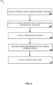
- FIG. 2 is an example process 200 for manufacturing a device with improved ambient temperature detection.
- the process 200 can be a process for manufacturing the device 100 described herein.
- the process 200 includes placing a printed circuit board within a housing (202).
- the printed circuit board may be the PCB 106.
- the housing may be the combination of the upper housing 110 with lower housing 112, and the interior space may be interior chamber formed when the upper housing 110 is joined to the lower housing 112.
- the housing may include the top surface 120.
- the housing may include a pass-through region that defines the through-hole 114 and may include the recess 116.
- the process 200 includes placing a flexible printed circuit substrate in an appropriate location (204).
- the flexible printed circuit substrate may be the substrate of the FPC 102.
- the flexible printed circuit substrate may include the first end region of the FPC 102 substrate that corresponds with the first region 140, the middle region of the FPC 102 substrate that corresponds with the second region 142, and the second end region of the FPC 102 substrate that corresponds with the third region 144.
- the process 200 includes placing a temperature sensor (206).
- the temperature sensor may be the temperature sensor 104.
- the temperature sensor may be placed at the second end region of the FPC 102 substrate in the recess 116 of the upper housing 110.
- the process 200 includes securing a first end region of the flexible printed circuit substrate (208).
- the first end region of the flexible printed circuit substrate may be the first end region of the FPC 102 substrate that corresponds with the first region 140.
- the first end region may be secured to the PCB 106 through one or more connectors, pins, or fingers.
- the first end region of the flexible printed circuit substrate may be secured to the PCB 106 using through-hole technology.
- the flexible printed circuit, which includes the flexible printed circuit substrate, and the printed circuit board are part of a single rigid-flex circuit.
- the flexible printed circuit is a flexible portion of the rigid-flex circuit and the printed circuit board is a rigid portion of the rigid-flex circuit.
- the process 200 includes placing a protective layer (210).
- the protective layer may be the layer 108.
- the protective layer may cover the temperature sensor 104, the recess 116, and/or the through-hole 114.
- embodiments of the invention can be implemented on a device having a display device, e.g., a CRT (cathode ray tube) or LCD (liquid crystal display) monitor, for displaying information to the user and a keyboard and a pointing device, e.g., a mouse, touch screen, trackpad, or a trackball, by which the user can provide input to the device.
- a display device e.g., a CRT (cathode ray tube) or LCD (liquid crystal display) monitor
- a keyboard and a pointing device e.g., a mouse, touch screen, trackpad, or a trackball
- Other kinds of devices can be used to provide for interaction with a user as well; for example, feedback provided to the user can be any form of sensory feedback, e.g., visual feedback, auditory feedback, or tactile feedback; and input from the user can be received in any form, including acoustic, speech, or tactile input.
Landscapes
- Physics & Mathematics (AREA)
- General Physics & Mathematics (AREA)
- Engineering & Computer Science (AREA)
- Microelectronics & Electronic Packaging (AREA)
- Nonlinear Science (AREA)
- Measuring Temperature Or Quantity Of Heat (AREA)
- Casings For Electric Apparatus (AREA)
- Structure Of Printed Boards (AREA)
Claims (15)
- Vorrichtung (100), umfassend:ein Gehäuse (110, 112), das einen Innenraum bildet und (i) eine Außenfläche und (ii) einen Durchgangsbereich, der ein Durchgangsloch (114) zwischen dem Innenraum und der Außenfläche definiert, beinhaltet;eine Leiterplatte (106), die in dem Innenraum des Gehäuses angeordnet ist;ein Substrat (102) für flexible gedruckte Schaltungen, das (i) einen ersten Endbereich, der mit der Leiterplatte verbunden ist, die in dem Innenraum des Gehäuses angeordnet ist, und (ii) einen zweiten Endbereich an einem dem ersten Endbereich gegenüberliegenden Ende des Substrats für flexible gedruckte Schaltungen beinhaltet, wobei der zweite Endbereich an der Außenfläche des Gehäuses angeordnet ist, wobei ein Abschnitt des Substrats für flexible gedruckte Schaltungen, der sich zwischen dem ersten Endbereich und dem zweiten Endbereich befindet, durch das Durchgangsloch verläuft;einen Temperatursensor (104), der an dem zweiten Endbereich des Substrats für flexible gedruckte Schaltungen an der Außenfläche des Gehäuses angeordnet ist; undeine Schutzschicht (108), die auf einem Abschnitt der Außenfläche des Gehäuses angeordnet ist und den Temperatursensor und das Durchgangsloch bedeckt.
- Vorrichtung nach Anspruch 1, wobei:der Temperatursensor auf einer ersten Seite des Substrats für flexible gedruckte Schaltungen angeordnet ist und die erste Seite des Substrats für flexible gedruckte Schaltungen der Schutzschicht zugewandt ist; und/oderder Temperatursensor in Kontakt mit der Schutzschicht steht.
- Vorrichtung nach Anspruch 1, wobei das Gehäuse eine Vertiefung an der Außenfläche umfasst, die an das Durchgangsloch angrenzt.
- Vorrichtung nach Anspruch 3, wobei die Vertiefung an der Außenfläche des Gehäuses einen tieferen Abschnitt zwischen zwei höheren Abschnitten aufweist.
- Vorrichtung nach Anspruch 4, wobei:ein erster höherer Abschnitt der zwei höheren Abschnitte der Vertiefung angrenzend an das Durchgangsloch positioniert ist;ein zweiter höherer Abschnitt der zwei höheren Abschnitte der Vertiefung entfernt von dem Durchgangsloch positioniert ist; undein Abschnitt des zweiten Endbereichs des Substrats für flexible gedruckte Schaltungen an dem zweiten höheren Abschnitt der zwei höheren Abschnitte der Vertiefung befestigt ist.
- Vorrichtung nach Anspruch 3, wobei der Temperatursensor in dem tieferen Abschnitt der Vertiefung an der Außenfläche des Gehäuses angeordnet ist.
- Vorrichtung nach Anspruch 4, wobei der Temperatursensor auf einer ersten Seite des Substrats für flexible gedruckte Schaltungen an dem zweiten Endbereich des Substrats für flexible gedruckte Schaltungen oberhalb des tieferen Abschnitts der Vertiefung an der Außenfläche des Gehäuses angeordnet ist.
- Vorrichtung nach Anspruch 7, wobei ein Spalt (128) zwischen einer zweiten Seite des Substrats für flexible gedruckte Schaltungen an dem zweiten Endbereich des Substrats für flexible gedruckte Schaltungen und dem tieferen Abschnitt der Vertiefung an der Außenfläche des Gehäuses ausgebildet ist.
- Vorrichtung nach Anspruch 4, wobei die Vertiefung an der Außenfläche des Gehäuses eine Breite, die geringfügig breiter als die Breite des zweiten Endbereichs des Substrats für flexible gedruckte Schaltungen ist, und eine Länge, die geringfügig länger als die Länge des zweiten Endbereichs des Substrats für flexible gedruckte Schaltungen ist, aufweist.
- Vorrichtung nach Anspruch 1, wobei der Durchgangsbereich des Gehäuses das Durchgangsloch derart definiert, dass das Durchgangsloch im Wesentlichen senkrecht in Bezug auf die Schutzschicht ist.
- Vorrichtung nach Anspruch 1, wobei die Schutzschicht aus einem Polymer gebildet ist, wobei das Polymer optional biaxial orientiertes Polyethylenterephthalat ist oder das Polymer Epoxid ist.
- Vorrichtung nach Anspruch 1, wobei die Schutzschicht aus einem Metall oder einem metallisierten Polymer, wie z. B. einem biaxial orientierten Polyethylenterephthalat, das eine Abscheidungsschicht aus Metall darauf aufweist, gebildet ist.
- Vorrichtung nach Anspruch 1, wobei die Schutzschicht ein Aufkleber ist, oder wobei die Schutzschicht durch einen Klebstoff an dem Abschnitt der Außenfläche des Gehäuses befestigt ist.
- Vorrichtung nach Anspruch 1, wobei:das Gehäuse eine obere Gehäuseeinheit, die eine obere Außenfläche aufweist, und eine untere Gehäuseeinheit enthält;die obere Gehäuseeinheit an der unteren Gehäuseeinheit befestigt ist; unddie Schutzschicht auf einem Abschnitt der oberen Außenfläche angeordnet ist.
- Verfahren, umfassend:Platzieren einer Leiterplatte (106) in einem Innenraum eines Gehäuses (110, 112), das (i) eine Außenfläche und (ii) einen Durchgangsbereich, der ein Durchgangsloch (114) zwischen dem Innenraum und der Außenfläche definiert, beinhaltet;Platzieren (i) eines ersten Endbereichs eines Substrats (102) für flexible gedruckte Schaltungen in dem Innenraum des Gehäuses und (ii) eines zweiten Endbereichs des Substrats für flexible gedruckte Schaltungen an einem dem ersten Endbereich gegenüberliegenden Ende des Substrats für flexible gedruckte Schaltungen an der Außenfläche des Gehäuses, wobei ein Abschnitt des Substrats für flexible gedruckte Schaltungen, der sich zwischen dem ersten Endbereich und dem zweiten Endbereich befindet, durch das Durchgangsloch hindurch platziert ist;Platzieren eines Temperatursensors (104) an dem zweiten Endbereich des Substrats für flexible gedruckte Schaltungen an der Außenfläche des Gehäuses;Befestigen des ersten Endbereichs des Substrats für flexible gedruckte Schaltungen an der Leiterplatte; undBedecken des Durchgangslochs und des Temperatursensors mit einer Schutzschicht (108).
Applications Claiming Priority (3)
| Application Number | Priority Date | Filing Date | Title |
|---|---|---|---|
| US16/456,093 US11366019B2 (en) | 2019-06-28 | 2019-06-28 | Enhanced ambient temperature detection |
| PCT/US2019/061453 WO2020263307A1 (en) | 2019-06-28 | 2019-11-14 | Enhanced ambient temperature detection |
| EP19818360.0A EP3973261B1 (de) | 2019-06-28 | 2019-11-14 | Verbesserte umgebungstemperaturdetektion |
Related Parent Applications (2)
| Application Number | Title | Priority Date | Filing Date |
|---|---|---|---|
| EP19818360.0A Division-Into EP3973261B1 (de) | 2019-06-28 | 2019-11-14 | Verbesserte umgebungstemperaturdetektion |
| EP19818360.0A Division EP3973261B1 (de) | 2019-06-28 | 2019-11-14 | Verbesserte umgebungstemperaturdetektion |
Publications (2)
| Publication Number | Publication Date |
|---|---|
| EP4155698A1 EP4155698A1 (de) | 2023-03-29 |
| EP4155698B1 true EP4155698B1 (de) | 2025-01-01 |
Family
ID=68848416
Family Applications (2)
| Application Number | Title | Priority Date | Filing Date |
|---|---|---|---|
| EP19818360.0A Active EP3973261B1 (de) | 2019-06-28 | 2019-11-14 | Verbesserte umgebungstemperaturdetektion |
| EP22201205.6A Active EP4155698B1 (de) | 2019-06-28 | 2019-11-14 | Verbesserte umgebungstemperaturdetektion |
Family Applications Before (1)
| Application Number | Title | Priority Date | Filing Date |
|---|---|---|---|
| EP19818360.0A Active EP3973261B1 (de) | 2019-06-28 | 2019-11-14 | Verbesserte umgebungstemperaturdetektion |
Country Status (5)
| Country | Link |
|---|---|
| US (2) | US11366019B2 (de) |
| EP (2) | EP3973261B1 (de) |
| JP (2) | JP7154446B2 (de) |
| CN (2) | CN114096818B (de) |
| WO (1) | WO2020263307A1 (de) |
Families Citing this family (6)
| Publication number | Priority date | Publication date | Assignee | Title |
|---|---|---|---|---|
| US11366019B2 (en) * | 2019-06-28 | 2022-06-21 | X Development Llc | Enhanced ambient temperature detection |
| JP6712793B1 (ja) * | 2020-02-13 | 2020-06-24 | パナソニックIpマネジメント株式会社 | 情報処理装置、及び、情報処理装置の製造方法 |
| JP7475238B2 (ja) * | 2020-08-06 | 2024-04-26 | 日本メクトロン株式会社 | 温度測定用装置 |
| EP4123274B1 (de) | 2021-07-19 | 2025-06-04 | TE Connectivity Sensors France | Sensor mit leiterplattenbasiertem kontakt |
| KR20230150037A (ko) | 2022-04-21 | 2023-10-30 | 삼성전자주식회사 | 전자 장치 및 그 전자 장치를 이용한 기온 측정 방법 |
| US12487128B2 (en) * | 2022-07-01 | 2025-12-02 | Samsara Inc. | Electronic device for monitoring vehicle environments |
Family Cites Families (33)
| Publication number | Priority date | Publication date | Assignee | Title |
|---|---|---|---|---|
| US5152610A (en) * | 1991-10-28 | 1992-10-06 | Hallett Stephen K | Pool thermometer |
| US5416728A (en) * | 1993-06-01 | 1995-05-16 | Chrysler Corporation | System and method for determining ambient temperature outside of a vehicle |
| US20050209813A1 (en) * | 2004-03-16 | 2005-09-22 | Johnson Controls Technology Company | Temperature sensing device |
| DE102004024955A1 (de) * | 2004-05-21 | 2005-12-15 | Trumpf Laser- Und Systemtechnik Gmbh | Temperatursensor und Temperaturüberwachungsvorrichtung |
| JP2006038824A (ja) * | 2004-06-25 | 2006-02-09 | Nippon Seiki Co Ltd | 半導体センサ装置 |
| US7229210B2 (en) * | 2005-05-23 | 2007-06-12 | Sang Il Yim | Self-standing fish tank thermometer |
| US9310098B2 (en) * | 2006-01-27 | 2016-04-12 | Emerson Electric Co. | Water heater control using external temperature sensor |
| DE102008028977A1 (de) * | 2008-06-18 | 2009-12-24 | Leopold Kostal Gmbh & Co. Kg | Sensoranordnung |
| EP2541157B1 (de) | 2011-06-27 | 2014-01-22 | Itron France | Heizkostenverteiler |
| JP2014534405A (ja) * | 2011-10-21 | 2014-12-18 | ネスト・ラブズ・インコーポレイテッド | ユーザフレンドリーな、ネットワーク接続された学習サーモスタットならびに関連するシステムおよび方法 |
| US9140613B2 (en) * | 2012-03-16 | 2015-09-22 | Zhejiang Dunan Hetian Metal Co., Ltd. | Superheat sensor |
| CN202856102U (zh) * | 2012-10-29 | 2013-04-03 | 杭州凯特电器有限公司 | 通过温度报警保护路由器的排插 |
| EP2808652B1 (de) * | 2013-05-31 | 2016-11-16 | Sensirion AG | Tragbare elektronische Vorrichtung mit integriertem Temperatursensor welcher durch andere Sensordaten compensiert wird. |
| DE102013212066A1 (de) * | 2013-06-25 | 2015-01-08 | Robert Bosch Gmbh | Modul für die Integration in ein mobiles Endgerät zur Messung der Umgebungstemperatur |
| WO2016028295A1 (en) | 2014-08-20 | 2016-02-25 | Leeo, Inc. | Electronic device for determining external temperature |
| US9909930B2 (en) * | 2015-02-24 | 2018-03-06 | Nxp B.V. | Multi-sensor assembly with tempature sensors having different thermal profiles |
| US10573938B2 (en) * | 2015-06-25 | 2020-02-25 | Te Connectivity Corporation | Battery module with a temperature monitoring assembly |
| US9606552B2 (en) * | 2015-08-26 | 2017-03-28 | Google Inc. | Thermostat with multiple sensing systems integrated therein |
| CN105450804B (zh) * | 2015-12-17 | 2019-06-21 | 青岛海信移动通信技术股份有限公司 | 一种移动终端 |
| US10359790B2 (en) * | 2016-02-12 | 2019-07-23 | Ademco Inc. | Multi piece HVAC controller housing with latches and guiding features |
| US9904811B2 (en) * | 2016-04-27 | 2018-02-27 | International Business Machines Corporation | Tamper-proof electronic packages with two-phase dielectric fluid |
| US10881349B2 (en) * | 2016-08-05 | 2021-01-05 | Bose Corporation | Temperature-monitoring earbud device |
| US10895883B2 (en) * | 2016-08-26 | 2021-01-19 | Ademco Inc. | HVAC controller with a temperature sensor mounted on a flex circuit |
| CN106742582A (zh) * | 2016-12-30 | 2017-05-31 | 宁波江北瑞臣工艺品设计有限公司 | 一种智能口香糖盒 |
| GB2573409B (en) * | 2017-01-31 | 2021-11-03 | Mitsubishi Electric Corp | Operation device |
| KR101994196B1 (ko) * | 2017-07-21 | 2019-07-01 | (주)초이스테크놀로지 | 체온측정장치 |
| CN207637021U (zh) * | 2017-07-30 | 2018-07-20 | 李乔 | 一种改进结构的控温范围内局部恒温控制器 |
| US10327326B2 (en) * | 2017-08-17 | 2019-06-18 | Apple Inc. | Electronic device with encapsulated circuit assembly having an integrated metal layer |
| CN207662532U (zh) * | 2018-01-22 | 2018-07-27 | 四川艾巴适环境科技有限公司 | 高精度温度检测装置 |
| US10697810B1 (en) * | 2018-07-11 | 2020-06-30 | Dickson/Unigage, Inc. | Sensor housing assembly |
| US11255897B2 (en) * | 2018-10-01 | 2022-02-22 | Cisco Technology, Inc. | Adjustable anchor for printed circuit board environmental sensor |
| CN208847408U (zh) * | 2018-10-30 | 2019-05-10 | 歌尔科技有限公司 | 充电针防水安装结构及腕戴设备 |
| US11366019B2 (en) | 2019-06-28 | 2022-06-21 | X Development Llc | Enhanced ambient temperature detection |
-
2019
- 2019-06-28 US US16/456,093 patent/US11366019B2/en active Active
- 2019-11-14 JP JP2021576334A patent/JP7154446B2/ja active Active
- 2019-11-14 WO PCT/US2019/061453 patent/WO2020263307A1/en not_active Ceased
- 2019-11-14 CN CN201980097982.1A patent/CN114096818B/zh active Active
- 2019-11-14 EP EP19818360.0A patent/EP3973261B1/de active Active
- 2019-11-14 CN CN202310615121.6A patent/CN116839751A/zh active Pending
- 2019-11-14 EP EP22201205.6A patent/EP4155698B1/de active Active
-
2022
- 2022-05-03 US US17/735,522 patent/US11852540B2/en active Active
- 2022-10-04 JP JP2022159881A patent/JP7239777B2/ja active Active
Also Published As
| Publication number | Publication date |
|---|---|
| CN114096818A (zh) | 2022-02-25 |
| US11852540B2 (en) | 2023-12-26 |
| EP3973261B1 (de) | 2023-01-11 |
| US11366019B2 (en) | 2022-06-21 |
| JP2022530703A (ja) | 2022-06-30 |
| EP4155698A1 (de) | 2023-03-29 |
| CN116839751A (zh) | 2023-10-03 |
| EP3973261A1 (de) | 2022-03-30 |
| US20220333999A1 (en) | 2022-10-20 |
| JP7239777B2 (ja) | 2023-03-14 |
| JP7154446B2 (ja) | 2022-10-17 |
| US20200408607A1 (en) | 2020-12-31 |
| JP2022186749A (ja) | 2022-12-15 |
| CN114096818B (zh) | 2023-05-09 |
| WO2020263307A1 (en) | 2020-12-30 |
Similar Documents
| Publication | Publication Date | Title |
|---|---|---|
| EP4155698B1 (de) | Verbesserte umgebungstemperaturdetektion | |
| US10327326B2 (en) | Electronic device with encapsulated circuit assembly having an integrated metal layer | |
| CN105404880B (zh) | 一种具有指纹传感器组件的电子装置 | |
| US9069201B2 (en) | Waterproof user interface display panels | |
| JP7293507B2 (ja) | 不透明面の背後の物体を検出するためのスキャナ | |
| CN110971727B (zh) | 电子设备 | |
| ES2270610T3 (es) | Medicion de temperatura de pantallas de cristal liquido en material adhesivo. | |
| US20190317634A1 (en) | Pressure sensitive display device | |
| EP2899519A1 (de) | Temperaturmessvorrichtung | |
| US10380406B2 (en) | Fingerprint sensor, method for manufacturing fingerprint sensor, and terminal | |
| CN212871536U (zh) | 一种带接触感应功能的温度检测组件及电子设备 | |
| CN115097710A (zh) | 防水型电子设备 | |
| US11513621B2 (en) | Display apparatus | |
| US20220011458A1 (en) | Scanner for detecting objects behind an opaque surface | |
| CN110028912B (zh) | 用于力敏式触摸传感器的泡沫带 | |
| TWI627574B (zh) | 觸控顯示裝置 | |
| KR20170130905A (ko) | 지문센서 모듈 | |
| JPH0434434Y2 (de) | ||
| JP2018044804A (ja) | デバイス | |
| JP2024533675A (ja) | 不透明面の背後に存在する物体を検出するためのスキャナ | |
| KR20150052491A (ko) | 모바일 장치용 지문 센서 모듈 및 이의 제조 방법 | |
| JP2010204034A (ja) | 面圧センサ | |
| JP2016206013A (ja) | センサーデバイス、携帯機器、電子機器及び移動体 | |
| JP2017227596A (ja) | 圧力センサー、高度計、電子機器および移動体 |
Legal Events
| Date | Code | Title | Description |
|---|---|---|---|
| PUAI | Public reference made under article 153(3) epc to a published international application that has entered the european phase |
Free format text: ORIGINAL CODE: 0009012 |
|
| STAA | Information on the status of an ep patent application or granted ep patent |
Free format text: STATUS: THE APPLICATION HAS BEEN PUBLISHED |
|
| AC | Divisional application: reference to earlier application |
Ref document number: 3973261 Country of ref document: EP Kind code of ref document: P |
|
| AK | Designated contracting states |
Kind code of ref document: A1 Designated state(s): AL AT BE BG CH CY CZ DE DK EE ES FI FR GB GR HR HU IE IS IT LI LT LU LV MC MK MT NL NO PL PT RO RS SE SI SK SM TR |
|
| STAA | Information on the status of an ep patent application or granted ep patent |
Free format text: STATUS: REQUEST FOR EXAMINATION WAS MADE |
|
| 17P | Request for examination filed |
Effective date: 20230906 |
|
| RBV | Designated contracting states (corrected) |
Designated state(s): AL AT BE BG CH CY CZ DE DK EE ES FI FR GB GR HR HU IE IS IT LI LT LU LV MC MK MT NL NO PL PT RO RS SE SI SK SM TR |
|
| GRAP | Despatch of communication of intention to grant a patent |
Free format text: ORIGINAL CODE: EPIDOSNIGR1 |
|
| STAA | Information on the status of an ep patent application or granted ep patent |
Free format text: STATUS: GRANT OF PATENT IS INTENDED |
|
| RIC1 | Information provided on ipc code assigned before grant |
Ipc: G01K 1/14 20210101AFI20240610BHEP |
|
| INTG | Intention to grant announced |
Effective date: 20240710 |
|
| GRAS | Grant fee paid |
Free format text: ORIGINAL CODE: EPIDOSNIGR3 |
|
| P01 | Opt-out of the competence of the unified patent court (upc) registered |
Free format text: CASE NUMBER: APP_57886/2024 Effective date: 20241023 |
|
| GRAA | (expected) grant |
Free format text: ORIGINAL CODE: 0009210 |
|
| STAA | Information on the status of an ep patent application or granted ep patent |
Free format text: STATUS: THE PATENT HAS BEEN GRANTED |
|
| AC | Divisional application: reference to earlier application |
Ref document number: 3973261 Country of ref document: EP Kind code of ref document: P |
|
| AK | Designated contracting states |
Kind code of ref document: B1 Designated state(s): AL AT BE BG CH CY CZ DE DK EE ES FI FR GB GR HR HU IE IS IT LI LT LU LV MC MK MT NL NO PL PT RO RS SE SI SK SM TR |
|
| REG | Reference to a national code |
Ref country code: GB Ref legal event code: FG4D |
|
| REG | Reference to a national code |
Ref country code: DE Ref legal event code: R096 Ref document number: 602019064501 Country of ref document: DE |
|
| REG | Reference to a national code |
Ref country code: CH Ref legal event code: EP |
|
| REG | Reference to a national code |
Ref country code: IE Ref legal event code: FG4D |
|
| REG | Reference to a national code |
Ref country code: LT Ref legal event code: MG9D |
|
| REG | Reference to a national code |
Ref country code: NL Ref legal event code: MP Effective date: 20250101 |
|
| REG | Reference to a national code |
Ref country code: AT Ref legal event code: MK05 Ref document number: 1756670 Country of ref document: AT Kind code of ref document: T Effective date: 20250101 |
|
| PG25 | Lapsed in a contracting state [announced via postgrant information from national office to epo] |
Ref country code: NL Free format text: LAPSE BECAUSE OF FAILURE TO SUBMIT A TRANSLATION OF THE DESCRIPTION OR TO PAY THE FEE WITHIN THE PRESCRIBED TIME-LIMIT Effective date: 20250101 |
|
| REG | Reference to a national code |
Ref country code: GB Ref legal event code: 732E Free format text: REGISTERED BETWEEN 20250605 AND 20250611 |
|
| REG | Reference to a national code |
Ref country code: DE Ref legal event code: R081 Ref document number: 602019064501 Country of ref document: DE Owner name: CHORUSVIEW, INC., LAS VEGAS, US Free format text: FORMER OWNER: X DEVELOPMENT LLC, MOUNTAIN VIEW, CA, US |
|
| PG25 | Lapsed in a contracting state [announced via postgrant information from national office to epo] |
Ref country code: FI Free format text: LAPSE BECAUSE OF FAILURE TO SUBMIT A TRANSLATION OF THE DESCRIPTION OR TO PAY THE FEE WITHIN THE PRESCRIBED TIME-LIMIT Effective date: 20250101 |
|
| PG25 | Lapsed in a contracting state [announced via postgrant information from national office to epo] |
Ref country code: PL Free format text: LAPSE BECAUSE OF FAILURE TO SUBMIT A TRANSLATION OF THE DESCRIPTION OR TO PAY THE FEE WITHIN THE PRESCRIBED TIME-LIMIT Effective date: 20250101 |
|
| PG25 | Lapsed in a contracting state [announced via postgrant information from national office to epo] |
Ref country code: ES Free format text: LAPSE BECAUSE OF FAILURE TO SUBMIT A TRANSLATION OF THE DESCRIPTION OR TO PAY THE FEE WITHIN THE PRESCRIBED TIME-LIMIT Effective date: 20250101 |
|
| PG25 | Lapsed in a contracting state [announced via postgrant information from national office to epo] |
Ref country code: NO Free format text: LAPSE BECAUSE OF FAILURE TO SUBMIT A TRANSLATION OF THE DESCRIPTION OR TO PAY THE FEE WITHIN THE PRESCRIBED TIME-LIMIT Effective date: 20250401 Ref country code: IS Free format text: LAPSE BECAUSE OF FAILURE TO SUBMIT A TRANSLATION OF THE DESCRIPTION OR TO PAY THE FEE WITHIN THE PRESCRIBED TIME-LIMIT Effective date: 20250501 |
|
| PG25 | Lapsed in a contracting state [announced via postgrant information from national office to epo] |
Ref country code: HR Free format text: LAPSE BECAUSE OF FAILURE TO SUBMIT A TRANSLATION OF THE DESCRIPTION OR TO PAY THE FEE WITHIN THE PRESCRIBED TIME-LIMIT Effective date: 20250101 |
|
| PG25 | Lapsed in a contracting state [announced via postgrant information from national office to epo] |
Ref country code: LV Free format text: LAPSE BECAUSE OF FAILURE TO SUBMIT A TRANSLATION OF THE DESCRIPTION OR TO PAY THE FEE WITHIN THE PRESCRIBED TIME-LIMIT Effective date: 20250101 Ref country code: PT Free format text: LAPSE BECAUSE OF FAILURE TO SUBMIT A TRANSLATION OF THE DESCRIPTION OR TO PAY THE FEE WITHIN THE PRESCRIBED TIME-LIMIT Effective date: 20250502 |
|
| PG25 | Lapsed in a contracting state [announced via postgrant information from national office to epo] |
Ref country code: BG Free format text: LAPSE BECAUSE OF FAILURE TO SUBMIT A TRANSLATION OF THE DESCRIPTION OR TO PAY THE FEE WITHIN THE PRESCRIBED TIME-LIMIT Effective date: 20250101 Ref country code: GR Free format text: LAPSE BECAUSE OF FAILURE TO SUBMIT A TRANSLATION OF THE DESCRIPTION OR TO PAY THE FEE WITHIN THE PRESCRIBED TIME-LIMIT Effective date: 20250402 |
|
| PG25 | Lapsed in a contracting state [announced via postgrant information from national office to epo] |
Ref country code: AT Free format text: LAPSE BECAUSE OF FAILURE TO SUBMIT A TRANSLATION OF THE DESCRIPTION OR TO PAY THE FEE WITHIN THE PRESCRIBED TIME-LIMIT Effective date: 20250101 |
|
| PG25 | Lapsed in a contracting state [announced via postgrant information from national office to epo] |
Ref country code: CZ Free format text: LAPSE BECAUSE OF FAILURE TO SUBMIT A TRANSLATION OF THE DESCRIPTION OR TO PAY THE FEE WITHIN THE PRESCRIBED TIME-LIMIT Effective date: 20250101 |
|
| RAP2 | Party data changed (patent owner data changed or rights of a patent transferred) |
Owner name: CHORUSVIEW, INC. |
|
| PG25 | Lapsed in a contracting state [announced via postgrant information from national office to epo] |
Ref country code: SE Free format text: LAPSE BECAUSE OF FAILURE TO SUBMIT A TRANSLATION OF THE DESCRIPTION OR TO PAY THE FEE WITHIN THE PRESCRIBED TIME-LIMIT Effective date: 20250101 |
|
| REG | Reference to a national code |
Ref country code: DE Ref legal event code: R097 Ref document number: 602019064501 Country of ref document: DE |
|
| PG25 | Lapsed in a contracting state [announced via postgrant information from national office to epo] |
Ref country code: SM Free format text: LAPSE BECAUSE OF FAILURE TO SUBMIT A TRANSLATION OF THE DESCRIPTION OR TO PAY THE FEE WITHIN THE PRESCRIBED TIME-LIMIT Effective date: 20250101 |
|
| PG25 | Lapsed in a contracting state [announced via postgrant information from national office to epo] |
Ref country code: DK Free format text: LAPSE BECAUSE OF FAILURE TO SUBMIT A TRANSLATION OF THE DESCRIPTION OR TO PAY THE FEE WITHIN THE PRESCRIBED TIME-LIMIT Effective date: 20250101 |
|
| PG25 | Lapsed in a contracting state [announced via postgrant information from national office to epo] |
Ref country code: IT Free format text: LAPSE BECAUSE OF FAILURE TO SUBMIT A TRANSLATION OF THE DESCRIPTION OR TO PAY THE FEE WITHIN THE PRESCRIBED TIME-LIMIT Effective date: 20250101 |
|
| PG25 | Lapsed in a contracting state [announced via postgrant information from national office to epo] |
Ref country code: EE Free format text: LAPSE BECAUSE OF FAILURE TO SUBMIT A TRANSLATION OF THE DESCRIPTION OR TO PAY THE FEE WITHIN THE PRESCRIBED TIME-LIMIT Effective date: 20250101 |
|
| PG25 | Lapsed in a contracting state [announced via postgrant information from national office to epo] |
Ref country code: RO Free format text: LAPSE BECAUSE OF FAILURE TO SUBMIT A TRANSLATION OF THE DESCRIPTION OR TO PAY THE FEE WITHIN THE PRESCRIBED TIME-LIMIT Effective date: 20250101 |
|
| PG25 | Lapsed in a contracting state [announced via postgrant information from national office to epo] |
Ref country code: SK Free format text: LAPSE BECAUSE OF FAILURE TO SUBMIT A TRANSLATION OF THE DESCRIPTION OR TO PAY THE FEE WITHIN THE PRESCRIBED TIME-LIMIT Effective date: 20250101 |
|
| PLBE | No opposition filed within time limit |
Free format text: ORIGINAL CODE: 0009261 |
|
| STAA | Information on the status of an ep patent application or granted ep patent |
Free format text: STATUS: NO OPPOSITION FILED WITHIN TIME LIMIT |
|
| 26N | No opposition filed |
Effective date: 20251002 |
|
| PGFP | Annual fee paid to national office [announced via postgrant information from national office to epo] |
Ref country code: DE Payment date: 20251126 Year of fee payment: 7 |
|
| PGFP | Annual fee paid to national office [announced via postgrant information from national office to epo] |
Ref country code: GB Payment date: 20251125 Year of fee payment: 7 |
|
| PGFP | Annual fee paid to national office [announced via postgrant information from national office to epo] |
Ref country code: FR Payment date: 20251125 Year of fee payment: 7 |