EP4131346A1 - Nitride semiconductor device, and method for manufacturing same - Google Patents
Nitride semiconductor device, and method for manufacturing same Download PDFInfo
- Publication number
- EP4131346A1 EP4131346A1 EP20926775.6A EP20926775A EP4131346A1 EP 4131346 A1 EP4131346 A1 EP 4131346A1 EP 20926775 A EP20926775 A EP 20926775A EP 4131346 A1 EP4131346 A1 EP 4131346A1
- Authority
- EP
- European Patent Office
- Prior art keywords
- nitride semiconductor
- layer
- substrate
- semiconductor layer
- graphene
- Prior art date
- Legal status (The legal status is an assumption and is not a legal conclusion. Google has not performed a legal analysis and makes no representation as to the accuracy of the status listed.)
- Pending
Links
Images



Classifications
-
- H—ELECTRICITY
- H10—SEMICONDUCTOR DEVICES; ELECTRIC SOLID-STATE DEVICES NOT OTHERWISE PROVIDED FOR
- H10D—INORGANIC ELECTRIC SEMICONDUCTOR DEVICES
- H10D30/00—Field-effect transistors [FET]
- H10D30/40—FETs having zero-dimensional [0D], one-dimensional [1D] or two-dimensional [2D] charge carrier gas channels
- H10D30/47—FETs having zero-dimensional [0D], one-dimensional [1D] or two-dimensional [2D] charge carrier gas channels having two-dimensional [2D] charge carrier gas channels, e.g. nanoribbon FETs or high electron mobility transistors [HEMT]
- H10D30/471—High electron mobility transistors [HEMT] or high hole mobility transistors [HHMT]
- H10D30/475—High electron mobility transistors [HEMT] or high hole mobility transistors [HHMT] having wider bandgap layer formed on top of lower bandgap active layer, e.g. undoped barrier HEMTs such as i-AlGaN/GaN HEMTs
-
- H—ELECTRICITY
- H10—SEMICONDUCTOR DEVICES; ELECTRIC SOLID-STATE DEVICES NOT OTHERWISE PROVIDED FOR
- H10W—GENERIC PACKAGES, INTERCONNECTIONS, CONNECTORS OR OTHER CONSTRUCTIONAL DETAILS OF DEVICES COVERED BY CLASS H10
- H10W40/00—Arrangements for thermal protection or thermal control
- H10W40/20—Arrangements for cooling
- H10W40/25—Arrangements for cooling characterised by their materials
- H10W40/254—Diamond
-
- C—CHEMISTRY; METALLURGY
- C01—INORGANIC CHEMISTRY
- C01B—NON-METALLIC ELEMENTS; COMPOUNDS THEREOF; METALLOIDS OR COMPOUNDS THEREOF NOT COVERED BY SUBCLASS C01C
- C01B32/00—Carbon; Compounds thereof
- C01B32/25—Diamond
- C01B32/28—After-treatment, e.g. purification, irradiation, separation or recovery
-
- C—CHEMISTRY; METALLURGY
- C01—INORGANIC CHEMISTRY
- C01B—NON-METALLIC ELEMENTS; COMPOUNDS THEREOF; METALLOIDS OR COMPOUNDS THEREOF NOT COVERED BY SUBCLASS C01C
- C01B32/00—Carbon; Compounds thereof
- C01B32/15—Nano-sized carbon materials
- C01B32/182—Graphene
-
- C—CHEMISTRY; METALLURGY
- C01—INORGANIC CHEMISTRY
- C01B—NON-METALLIC ELEMENTS; COMPOUNDS THEREOF; METALLOIDS OR COMPOUNDS THEREOF NOT COVERED BY SUBCLASS C01C
- C01B32/00—Carbon; Compounds thereof
- C01B32/15—Nano-sized carbon materials
- C01B32/182—Graphene
- C01B32/184—Preparation
-
- H—ELECTRICITY
- H10—SEMICONDUCTOR DEVICES; ELECTRIC SOLID-STATE DEVICES NOT OTHERWISE PROVIDED FOR
- H10D—INORGANIC ELECTRIC SEMICONDUCTOR DEVICES
- H10D30/00—Field-effect transistors [FET]
- H10D30/01—Manufacture or treatment
- H10D30/015—Manufacture or treatment of FETs having heterojunction interface channels or heterojunction gate electrodes, e.g. HEMT
-
- H—ELECTRICITY
- H10—SEMICONDUCTOR DEVICES; ELECTRIC SOLID-STATE DEVICES NOT OTHERWISE PROVIDED FOR
- H10D—INORGANIC ELECTRIC SEMICONDUCTOR DEVICES
- H10D30/00—Field-effect transistors [FET]
- H10D30/01—Manufacture or treatment
- H10D30/061—Manufacture or treatment of FETs having Schottky gates
-
- H—ELECTRICITY
- H10—SEMICONDUCTOR DEVICES; ELECTRIC SOLID-STATE DEVICES NOT OTHERWISE PROVIDED FOR
- H10D—INORGANIC ELECTRIC SEMICONDUCTOR DEVICES
- H10D62/00—Semiconductor bodies, or regions thereof, of devices having potential barriers
- H10D62/10—Shapes, relative sizes or dispositions of the regions of the semiconductor bodies; Shapes of the semiconductor bodies
- H10D62/17—Semiconductor regions connected to electrodes not carrying current to be rectified, amplified or switched, e.g. channel regions
- H10D62/351—Substrate regions of field-effect devices
- H10D62/357—Substrate regions of field-effect devices of FETs
-
- H—ELECTRICITY
- H10—SEMICONDUCTOR DEVICES; ELECTRIC SOLID-STATE DEVICES NOT OTHERWISE PROVIDED FOR
- H10P—GENERIC PROCESSES OR APPARATUS FOR THE MANUFACTURE OR TREATMENT OF DEVICES COVERED BY CLASS H10
- H10P14/00—Formation of materials, e.g. in the shape of layers or pillars
- H10P14/20—Formation of materials, e.g. in the shape of layers or pillars of semiconductor materials
- H10P14/29—Formation of materials, e.g. in the shape of layers or pillars of semiconductor materials characterised by the substrates
- H10P14/2901—Materials
- H10P14/2902—Materials being Group IVA materials
- H10P14/2903—Carbon, e.g. diamond-like carbon
-
- H—ELECTRICITY
- H10—SEMICONDUCTOR DEVICES; ELECTRIC SOLID-STATE DEVICES NOT OTHERWISE PROVIDED FOR
- H10P—GENERIC PROCESSES OR APPARATUS FOR THE MANUFACTURE OR TREATMENT OF DEVICES COVERED BY CLASS H10
- H10P14/00—Formation of materials, e.g. in the shape of layers or pillars
- H10P14/20—Formation of materials, e.g. in the shape of layers or pillars of semiconductor materials
- H10P14/29—Formation of materials, e.g. in the shape of layers or pillars of semiconductor materials characterised by the substrates
- H10P14/2901—Materials
- H10P14/2902—Materials being Group IVA materials
- H10P14/2904—Silicon carbide
-
- H—ELECTRICITY
- H10—SEMICONDUCTOR DEVICES; ELECTRIC SOLID-STATE DEVICES NOT OTHERWISE PROVIDED FOR
- H10P—GENERIC PROCESSES OR APPARATUS FOR THE MANUFACTURE OR TREATMENT OF DEVICES COVERED BY CLASS H10
- H10P14/00—Formation of materials, e.g. in the shape of layers or pillars
- H10P14/20—Formation of materials, e.g. in the shape of layers or pillars of semiconductor materials
- H10P14/32—Formation of materials, e.g. in the shape of layers or pillars of semiconductor materials characterised by intermediate layers between substrates and deposited layers
- H10P14/3202—Materials thereof
- H10P14/3204—Materials thereof being Group IVA semiconducting materials
- H10P14/3206—Carbon, e.g. diamond-like carbon
-
- H—ELECTRICITY
- H10—SEMICONDUCTOR DEVICES; ELECTRIC SOLID-STATE DEVICES NOT OTHERWISE PROVIDED FOR
- H10P—GENERIC PROCESSES OR APPARATUS FOR THE MANUFACTURE OR TREATMENT OF DEVICES COVERED BY CLASS H10
- H10P14/00—Formation of materials, e.g. in the shape of layers or pillars
- H10P14/20—Formation of materials, e.g. in the shape of layers or pillars of semiconductor materials
- H10P14/32—Formation of materials, e.g. in the shape of layers or pillars of semiconductor materials characterised by intermediate layers between substrates and deposited layers
- H10P14/3202—Materials thereof
- H10P14/3214—Materials thereof being Group IIIA-VA semiconductors
- H10P14/3216—Nitrides
-
- H—ELECTRICITY
- H10—SEMICONDUCTOR DEVICES; ELECTRIC SOLID-STATE DEVICES NOT OTHERWISE PROVIDED FOR
- H10P—GENERIC PROCESSES OR APPARATUS FOR THE MANUFACTURE OR TREATMENT OF DEVICES COVERED BY CLASS H10
- H10P14/00—Formation of materials, e.g. in the shape of layers or pillars
- H10P14/20—Formation of materials, e.g. in the shape of layers or pillars of semiconductor materials
- H10P14/32—Formation of materials, e.g. in the shape of layers or pillars of semiconductor materials characterised by intermediate layers between substrates and deposited layers
- H10P14/3242—Structure
- H10P14/3244—Layer structure
- H10P14/3251—Layer structure consisting of three or more layers
-
- H—ELECTRICITY
- H10—SEMICONDUCTOR DEVICES; ELECTRIC SOLID-STATE DEVICES NOT OTHERWISE PROVIDED FOR
- H10P—GENERIC PROCESSES OR APPARATUS FOR THE MANUFACTURE OR TREATMENT OF DEVICES COVERED BY CLASS H10
- H10P14/00—Formation of materials, e.g. in the shape of layers or pillars
- H10P14/20—Formation of materials, e.g. in the shape of layers or pillars of semiconductor materials
- H10P14/34—Deposited materials, e.g. layers
- H10P14/3402—Deposited materials, e.g. layers characterised by the chemical composition
- H10P14/3414—Deposited materials, e.g. layers characterised by the chemical composition being group IIIA-VIA materials
- H10P14/3416—Nitrides
-
- H—ELECTRICITY
- H10—SEMICONDUCTOR DEVICES; ELECTRIC SOLID-STATE DEVICES NOT OTHERWISE PROVIDED FOR
- H10P—GENERIC PROCESSES OR APPARATUS FOR THE MANUFACTURE OR TREATMENT OF DEVICES COVERED BY CLASS H10
- H10P95/00—Generic processes or apparatus for manufacture or treatments not covered by the other groups of this subclass
- H10P95/11—Separation of active layers from substrates
-
- H—ELECTRICITY
- H10—SEMICONDUCTOR DEVICES; ELECTRIC SOLID-STATE DEVICES NOT OTHERWISE PROVIDED FOR
- H10W—GENERIC PACKAGES, INTERCONNECTIONS, CONNECTORS OR OTHER CONSTRUCTIONAL DETAILS OF DEVICES COVERED BY CLASS H10
- H10W99/00—Subject matter not provided for in other groups of this subclass
-
- H—ELECTRICITY
- H10—SEMICONDUCTOR DEVICES; ELECTRIC SOLID-STATE DEVICES NOT OTHERWISE PROVIDED FOR
- H10D—INORGANIC ELECTRIC SEMICONDUCTOR DEVICES
- H10D62/00—Semiconductor bodies, or regions thereof, of devices having potential barriers
- H10D62/80—Semiconductor bodies, or regions thereof, of devices having potential barriers characterised by the materials
- H10D62/85—Semiconductor bodies, or regions thereof, of devices having potential barriers characterised by the materials being Group III-V materials, e.g. GaAs
- H10D62/8503—Nitride Group III-V materials, e.g. AlN or GaN
Definitions
- a silicon carbide substrate 30 is prepared as illustrated in FIG. 3 .
- the silicon carbide substrate 30 has a cubic or hexagonal crystal structure.
- An upper surface of the silicon carbide substrate 30 is flattened at a level of atomic layer using a known method such as mechanical polishing, chemical mechanical polishing, dry etching, or wet etching, for example, and a surface roughness is smaller than 1.0 nm, and is more preferably smaller than 0.5 nm.
- a silicon atom on a surface of the silicon carbide substrate 30 is desorbed from the silicon carbide substrate 30 in accordance with such a thermal treatment, and a remaining carbon atom forms the graphene layer 40 taking over a crystal structure of the silicon carbide substrate 30.
- the graphene layer is formed on the silicon carbide substrate 30 by such a method, thus the graphene layer 40 having low surface roughness with a controlled number of layers and having extremely little lattice defect can be provided on a whole surface of the silicon carbide substrate 30.
- a thickness of the graphene layer 40 is 0.6 nm to 0.7 nm (6 to 7 ⁇ ), for example.
- FIG. 8 and FIG. 9 Described next using FIG. 8 and FIG. 9 is a step of fixing the nitride semiconductor layer on the diamond substrate to form the nitride semiconductor device. Firstly, in a step illustrated in FIG. 8 , the diamond substrate 10 illustrated in FIG. 2 is bonded to the nitride semiconductor layer 50 separated from the silicon carbide substrate 30.
Landscapes
- Chemical & Material Sciences (AREA)
- Organic Chemistry (AREA)
- Inorganic Chemistry (AREA)
- Engineering & Computer Science (AREA)
- Materials Engineering (AREA)
- Nanotechnology (AREA)
- Life Sciences & Earth Sciences (AREA)
- General Life Sciences & Earth Sciences (AREA)
- Geology (AREA)
- Recrystallisation Techniques (AREA)
- Junction Field-Effect Transistors (AREA)
Abstract
Description
- The present invention relates to a nitride semiconductor device, and particularly to a nitride semiconductor device having a high heat dissipation property.
- A field effect transistor, especially a high electron mobility transistor (HEMT), using gallium nitride (GaN), aluminum nitride (AlN), indium nitride (InN), or a semiconductor made up of a combination thereof is known as a semiconductor device operating in a high output region. Such a nitride semiconductor device is used for a high output power amplifier and a high power switching device, for example.
- Such a nitride semiconductor device has a significant reduction in electrical characteristics and reliability due to increase in temperature during a high power operation. Thus, there is a need to provide a material having a high heat dissipation property near a heat generation source to suppress increase in temperature of the nitride semiconductor device. For example, a nitride semiconductor layer is processed and bonded to a heat spreading material to be able to increase the heat dissipation property.
- In particular, diamond is a material having a maximum thermal conductivity in solid materials, and has a preferable property as a heat spreading material. Thus, known as disclosed in Patent Document 1, for example, is a technique of bonding a diamond substrate and a nitride semiconductor layer via an amorphous carbon layer to increase a heat dissipation property of a nitride semiconductor device.
- The nitride semiconductor layer used for a nitride semiconductor device having such a configuration can be formed on a substrate of silicon (Si), silicon carbide (SiC), or sapphire (Al2O3), for example, by a heteroepitaxial growth technique, however, a heteroepitaxial growth technique of growing the nitride semiconductor layer on the diamond substrate is not yet established.
- Accordingly, only the nitride semiconductor layer needs to be taken out after the nitride semiconductor layer is formed on the heteroepitaxial growth substrate and transferred on the diamond substrate to form the nitride semiconductor layer on the diamond substrate.
- Patent Document 1: Japanese Patent Application Laid-Open
JP 2018-206955 A - However, in a case of the semiconductor device described in said Patent Document 1, a step of manufacturing the semiconductor device includes a step of removing a heteroepitaxial growth substrate of the nitride semiconductor layer by grinding and chemical mechanical polishing (CMP). Thus, there is a problem that a manufacturing cost increases.
- The present invention therefore has been made to solve problems as described above, and it is an object to provide a nitride semiconductor device having a high heat dissipation property at low cost.
- A nitride semiconductor device according to the present invention includes: a diamond substrate; a first graphene layer provided on the diamond substrate; a second graphene layer provided on the first graphene layer; a nitride semiconductor layer provided on the second graphene layer; and a nitride semiconductor element having an electrode provided on the nitride semiconductor layer, wherein the first and second graphene layers are provided as an interface layer between the diamond substrate and the nitride semiconductor layer.
- According to the nitride semiconductor device described above, a nitride semiconductor device in which a nitride semiconductor element is provided on a diamond substrate having an extremely high heat dissipation property can be achieved at low cost.
-
- FIG. 1
- A cross-sectional view schematically illustrating a configuration of a nitride semiconductor device according to an Embodiment 1.
- FIG. 2
- A cross-sectional view for explaining a method of manufacturing the nitride semiconductor device according to the Embodiment 1.
- FIG. 3
- A cross-sectional view for explaining a method of manufacturing the nitride semiconductor device according to the Embodiment 1.
- FIG. 4
- A cross-sectional view for explaining a method of manufacturing the nitride semiconductor device according to the Embodiment 1.
- FIG. 5
- A cross-sectional view for explaining a method of manufacturing the nitride semiconductor device according to the Embodiment 1.
- FIG. 6
- A cross-sectional view for explaining a method of manufacturing the nitride semiconductor device according to the Embodiment 1.
- FIG. 7
- A cross-sectional view for explaining a method of manufacturing the nitride semiconductor device according to the Embodiment 1.
- FIG. 8
- A cross-sectional view for explaining a method of manufacturing the nitride semiconductor device according to the Embodiment 1.
- FIG. 9
- A cross-sectional view for explaining a method of manufacturing the nitride semiconductor device according to the Embodiment 1.
- FIG. 10
- A cross-sectional view for explaining a method of manufacturing the nitride semiconductor device according to an Embodiment 2.
- FIG. 11
- A cross-sectional view for explaining a method of manufacturing the nitride semiconductor device according to the Embodiment 2.
- FIG. 12
- A cross-sectional view for explaining a method of manufacturing the nitride semiconductor device according to the Embodiment 2.
- FIG. 13
- A cross-sectional view for explaining a method of manufacturing the nitride semiconductor device according to the Embodiment 2.
- FIG. 14
- A cross-sectional view for explaining a method of manufacturing the nitride semiconductor device according to the Embodiment 2.
- FIG. 15
- A cross-sectional view for explaining a method of manufacturing the nitride semiconductor device according to the Embodiment 2.
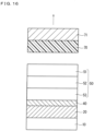
- FIG. 16
- A cross-sectional view for explaining a method of manufacturing the nitride semiconductor device according to the Embodiment 2.
- FIG. 17
- A cross-sectional view for explaining a method of manufacturing the nitride semiconductor device according to the Embodiment 2.
- An embodiment is described hereinafter with reference to the drawings. The drawings are schematically illustrated, thus a dimension of each constituent element in the drawings in a horizontal direction and a vertical direction does not accurately express an actual dimension, and an aspect ratio is not accurate. In the description hereinafter, the same reference numerals are assigned to the similar constituent elements in the illustration, and the same applies to names and functions thereof. Thus, a detailed description thereof may be omitted in some cases.
- Used in the description hereinafter are terms each indicating a specific position and direction such as "upper", "lower", and "side", for example, however, these terms are used for convenience of easy understanding of contents of the embodiments, and do not relate to a direction in an actual use.
- "A nitride semiconductor" in the description hereinafter is a collective term of a semiconductor including GaN, AlN, InN and an intermediate composition thereof.
- With respect to a conductivity type of an impurity, an n type is generally defined as "a first conductivity type" and a p type is defined as "a second conductivity type", however, a reverse definition is also applicable.
-
FIG. 1 is a cross-sectional view schematically illustrating a configuration of anitride semiconductor device 100 according to an Embodiment 1. A semiconductor device according to the Embodiment 1 includes adiamond substrate 10, a graphene layer 20 (first graphene layer) provided on thediamond substrate 10, a graphene layer 40 (second graphene layer) provided on thegraphene layer 20, anitride semiconductor layer 50 provided on thegraphene layer 40, asource electrode 60 selectively provided on thenitride semiconductor layer 50, adrain electrode 61 selectively provided separately from thesource electrode 60, and agate electrode 62 provided between thesource electrode 60 and thedrain electrode 61. A nitride semiconductor element made up of thenitride semiconductor layer 50, thesource electrode 60 provided on thenitride semiconductor layer 50, adrain electrode 61, and agate electrode 62 constitutes an HEMT. - Described next is a method of manufacturing the
nitride semiconductor device 100. The manufacturing method according to the Embodiment 1 roughly includes the following four steps. That is to say, the manufacturing method includes a step of forming a graphene layer on a diamond substrate, a step of forming a nitride semiconductor layer on a silicon carbide substrate, a step of separating the silicon carbide substrate and the nitride semiconductor layer to fix the nitride semiconductor layer to a support substrate, and a step of fixing the nitride semiconductor layer on the diamond substrate to form a nitride semiconductor device. - Described firstly using
FIG. 2 is a step of forming a graphene layer on a diamond substrate. Firstly, adiamond substrate 10 is prepared as illustrated inFIG. 2 . A single crystal diamond substrate, a polycrystalline diamond substrate, or a substrate including a single crystal diamond and a polycrystalline diamond can be used as thediamond substrate 10, and the substrate having a thermal conductivity of 1000 W ▪ m-1 ▪ K-1 or more is preferably used. An upper surface of thediamond substrate 10 is flattened at a level of atomic layer using a known method such as mechanical polishing, chemical mechanical polishing, dry etching, or wet etching, for example, and a surface roughness is smaller than 1.0 nm, and is more preferably smaller than 0.5 nm. - Next, the
graphene layer 20 is formed on thediamond substrate 10 as illustrated inFIG. 2 . As a method of forming thegraphene layer 20, thegraphene layer 20 is formed by performing a thermal treatment at a temperature of 800 °C to 1400 °C under vacuum or inactive gas atmosphere of 1.333 ×101 Pa (1×10⁻¹ Torr) or less. - A heating temperature is more preferably within a range of 1000 °C to 1300 °C. According to such a thermal treatment, a carbon atom on the surface of the
diamond substrate 10 is reconstructed, and thegraphene layer 20 taking over a crystal structure of thediamond substrate 10 is formed. Thegraphene layer 20 is formed on thediamond substrate 10 by such a method, thus thegraphene layer 20 having a high surface flatness with a controlled number of layers and having extremely low lattice defect can be provided on a whole surface of thediamond substrate 10. A thickness of thegraphene layer 20 is 0.6 to 0.7 nm (6 to 7 Å), for example. - Examples of a method of forming the
graphene layer 20 include chemical vapor deposition using methane gas as a material. However, thegraphene layer 20 can be formed more simply by using a method using the thermal treatment described above than a case of using the chemical vapor deposition. - The graphene layer formed on the single crystal diamond substrate has low lattice defect compared with the graphene layer formed on the polycrystalline diamond substrate. Examples of a substrate including the single crystal diamond and polycrystalline diamond can include a substrate in which some of single crystal diamond substrates are planarly arranged, and the polycrystalline diamond is formed between the substrates by chemical vapor deposition to connect the single crystal diamond substrates.
- Next, a step of forming a nitride semiconductor layer on a silicon carbide substrate is described using
FIG. 3 andFIG. 4 . Firstly, asilicon carbide substrate 30 is prepared as illustrated inFIG. 3 . Thesilicon carbide substrate 30 has a cubic or hexagonal crystal structure. An upper surface of thesilicon carbide substrate 30 is flattened at a level of atomic layer using a known method such as mechanical polishing, chemical mechanical polishing, dry etching, or wet etching, for example, and a surface roughness is smaller than 1.0 nm, and is more preferably smaller than 0.5 nm. - Next, the
graphene layer 40 is formed on thesilicon carbide substrate 30 as illustrated inFIG. 3 . Thegraphene layer 40 is formed by performing a thermal treatment under hydrogen atmosphere and a thermal treatment under vacuum on thesilicon carbide substrate 30. A temperature of the thermal treatment is within a range of 1400 °C to 1600 °C and is preferably 1550 °C to 1600 °C. The thermal treatment under hydrogen atmosphere is a preparation step for forming thegraphene 40, and the graphene layer is formed by the subsequent thermal treatment under vacuum. Pressure of hydrogen atmosphere is approximately 3.999 × 10³ Pa (30 Torr), for example. Thegraphene layer 40 may be formed using a thermal treatment under inactive gas atmosphere in place of the thermal treatment under vacuum. A temperature of the thermal treatment in this case is also within a range of 1400 °C to 1600 °C, and is preferably 1550 °C to 1600 °C. - A silicon atom on a surface of the
silicon carbide substrate 30 is desorbed from thesilicon carbide substrate 30 in accordance with such a thermal treatment, and a remaining carbon atom forms thegraphene layer 40 taking over a crystal structure of thesilicon carbide substrate 30. The graphene layer is formed on thesilicon carbide substrate 30 by such a method, thus thegraphene layer 40 having low surface roughness with a controlled number of layers and having extremely little lattice defect can be provided on a whole surface of thesilicon carbide substrate 30. A thickness of thegraphene layer 40 is 0.6 nm to 0.7 nm (6 to 7 Å), for example. - Examples of a method of forming the
graphene layer 40 also include chemical vapor deposition using methane gas. However, thegraphene layer 40 can be formed more simply by using a method using the thermal treatment described above than a case of using the chemical vapor deposition. - Next, the
nitride semiconductor layer 50 is formed on thegraphene layer 40 by heteroepitaxial growth in the step illustrated inFIG. 4 . Applicable as a method of forming thenitride semiconductor layer 50 is molecular beam epitaxy using metal gallium and active nitrogen or metal-organic chemical vapor deposition using trimethyl gallium and ammonia. Thenitride semiconductor layer 50 has a configuration that a buffer layer 53 (first nitride semiconductor layer) made of AlN or AlGaN, for example, a channel layer 52 (second nitride semiconductor layer) made of GaN, for example, and a barrier layer 51 (third nitride semiconductor layer) made of AlGaN (aluminum gallium nitride) are stacked on thegraphene layer 40 in this order. An example of thicknesses of these layers is that thebarrier layer 51 is 25 nm, thechannel layer 52 is 1 µm, and thebuffer layer 53 is 500 nm. - The
channel layer 52 may include impurity such as iron (Fe) or carbon (C) for purpose of achieving high resistance. Hetero junction is formed in an interface between thechannel layer 52 and thebarrier layer 51, and thebarrier layer 51 supplies electrons to the interface, thus two dimensional electron gas (2DEG) is formed in the interface. The 2DEG serves as a carrier of the nitride semiconductor device of the present embodiment. Thebuffer layer 53 suppresses crystal defect caused by a lattice mismatch of thesilicon carbide substrate 30 and thegraphene layer 40 and a lattice constant of the nitride semiconductor. - Next, in a step illustrated in
FIG. 5 , thesource electrode 60, thedrain electrode 61, and thegate electrode 62 are selectively formed on thenitride semiconductor layer 50. Thesource electrode 60 and thedrain electrode 61 are metal electrodes, for example, and is made of aluminum, for example. Ohmic contact is preferably formed between thesource electrode 60 and thenitride semiconductor layer 50 and between thedrain electrode 61 and thenitride semiconductor layer 50. - A thickness of each of the
source electrode 60 and thedrain electrode 61 is 1 µm, for example, and a thickness of thegate electrode 62 is 200 nm, for example, and all of them are formed by vacuum deposition, sputtering, or chemical vapor deposition. - Ion implantation may be performed on a semiconductor region below the source electrode 60 (referred to as the source electrode region hereinafter) and a semiconductor region below the drain electrode (the drain electrode region) to have an n-type conductivity. Silicon, for example, is ion-implanted as n-type impurity to have the n-type conductivity. A dose amount of the n-type impurity is 1 ×1015 cm-2, for example. The impurity is activated by a thermal treatment after implantation. The
gate electrode 62 may be made of metal such as nickel (Ni) or platinum (Pt), p-type polysilicon doped with boron, or n-type polysilicon doped with phosphorus, for example. - Next, a step of separating a nitride silicon substrate and a nitride semiconductor layer is described using
FIG. 6 andFIG. 7 . Firstly, in a step illustrated inFIG. 6 , asupport substrate 71 is bonded to thenitride semiconductor layer 50 on thesilicon carbide substrate 30 using a supportsubstrate adhesive layer 70. - The support
substrate adhesive layer 70 is preferably formed by applying an organic adhesive agent removable with an organic solution, for example, or an adhesive agent which can be removed with heating or ultraviolet irradiation to cover thesource electrode 60, thedrain electrode 61, and thegate electrode 62. Two or more adhesive layers may be overlapped with each other. Thesupport substrate 71 is made of Si, sapphire, or glass, for example. - Next, in a step illustrated in
FIG. 7 , thenitride semiconductor layer 50 to which thesupport substrate 71 is bonded is pulled upward or downward while thesilicon carbide substrate 30 is fixed, thus thesilicon carbide substrate 30 and thenitride semiconductor layer 50 are separated from each other. - Force of pulling the
support substrate 71 may be set to any of a magnitude of separating thesilicon carbide substrate 30 and thegraphene layer 40 at the interface therebetween and a magnitude of interlayer-separating thegraphene layer 40. Thesilicon carbide substrate 30 is fixed to a supporter not shown in the drawings by vacuum suction or using an adhesive agent, for example. Force within a range from 10 N▪mm-2 to 10000 N▪mm-2, for example, is appropriately added as force of pulling thesupport substrate 71. That is to say, pulling force is added to separate thenitride semiconductor layer 50 and thesilicon carbide substrate 30, and at this time, the pulling force is gradually increased from a small value, and the pulling is stopped at a time when thenitride semiconductor layer 50 and thesilicon carbide substrate 30 are separated from each other. In this manner, force in a magnitude of separating thesilicon carbide substrate 30 and thegraphene layer 40 at the interface therebetween or a magnitude of interlayer-separating thegraphene layer 40 may be appropriately added as the pulling force. - It is also applicable that the
silicon carbide substrate 30 and thenitride semiconductor layer 50 are separated from each other by pulling thesilicon carbide substrate 30 upward or downward while thesupport substrate 71 is fixed. - Also applicable as a method of separating the
silicon carbide substrate 30 and thenitride semiconductor layer 50 is that stress caused by a volume change in accordance with heating or cooling using a difference in coefficient of thermal expansion between graphene and silicon carbide. -
FIG. 7 illustrates a state where thegraphene layer 40 is interlayer-separated, and it is most preferable that thesilicon carbide substrate 30 and thegraphene layer 40 are separated at the interface therebetween and thewhole graphene layer 40 is located on thenitride semiconductor layer 50. - By separating them in this manner, a surface of the
graphene layer 40 on a side of thenitride semiconductor layer 50 is flat after separation, and enters a preferable state when thegraphene layer 40 is bonded to thegraphene layer 20 on thediamond substrate 10 in a subsequent step. - The
nitride semiconductor layer 50 and thesilicon carbide substrate 30 are separated by the method described above, thus thenitride semiconductor layer 50 can be isolated while leaving thesilicon carbide substrate 30. That is to say, thesilicon carbide substrate 30 is not mechanically or chemically removed, thus thesilicon carbide substrate 30 as the heteroepitaxial substrate of thenitride semiconductor layer 50 can be reused, and a manufacturing cost of thenitride semiconductor device 100 can be reduced. - Described next using
FIG. 8 andFIG. 9 is a step of fixing the nitride semiconductor layer on the diamond substrate to form the nitride semiconductor device. Firstly, in a step illustrated inFIG. 8 , thediamond substrate 10 illustrated inFIG. 2 is bonded to thenitride semiconductor layer 50 separated from thesilicon carbide substrate 30. - The
graphene layer 20 on thediamond substrate 10 illustrated inFIG. 2 has an atomic arrangement similar to thegraphene layer 40 remaining below thenitride semiconductor layer 50. Thegraphene layer 20 and thegraphene layer 40 have contact with each other, thus physical bonding is formed by van der Waals force which occurs between thegraphene layer 20 and thegraphene layer 40. At a time of bonding, a clean room or a clean booth having little dust particles in an atmosphere is preferably used to suppress particle inclusion in a bonding interface. Bonding can be performed at atmospheric pressure, however, when bonding is performed in vacuum, remaining air in the bonding interface can be suppressed. Both thegraphene layer 20 and thegraphene layer 40 are graphene layers having high surface flatness with a controlled number of layers, thus occurrence of a void in the bonding interface can be suppressed. - The graphene is a high thermal conductive material, and the
graphene layer 20 and thegraphene layer 40 have little lattice defect. Accordingly, thenitride semiconductor layer 50 and thediamond substrate 10 can be bonded via an interface layer having extremely small thermal resistance, that is to say, a bonding layer made up of thegraphene layer 20 and thegraphene layer 40. A thermal conductivity of the graphene layer is approximately 2000 to 5000 W▪m-1▪K-1 in an in-plane direction and is approximately 10 W▪m-1- K-1 in a direction vertical to the in-plane direction, for example, at room temperature. - Next, in a step illustrated in
FIG. 9 , thesupport substrate 71 is separated from thenitride semiconductor layer 50 on thediamond substrate 10. Thediamond substrate 10 to which thenitride semiconductor layer 50 is bonded is heated or ultraviolet light is irradiated to the supportsubstrate adhesive layer 70 so that the supportsubstrate adhesive layer 70 has detachability, and the supportsubstrate adhesive layer 70 is separated to separate thesupport substrate 71 together with the supportsubstrate adhesive layer 70 from thenitride semiconductor layer 50 on thediamond substrate 10. According to this step, the nitride semiconductor device 100 (FIG. 1 ) having the nitride semiconductor element (HEMT) made up of thenitride semiconductor layer 50, thesource electrode 60, thedrain electrode 61, and thegate electrode 62 can be obtained. - As described above, the
nitride semiconductor device 100 according to the Embodiment 1 includes thediamond substrate 10 having a high thermal conductivity. The bonding layer made up of the graphene layers 20 and 40 having extremely little lattice defect and a high thermal transport property has a thickness of two atomic layers to several tens of atomic layers between thenitride semiconductor layer 50 and thediamond substrate 10. - Thus, achieved is a nitride semiconductor device having a more preferable thermal conductivity between the
nitride semiconductor layer 50 and thediamond substrate 10 and a higher heat dissipation property than a configuration that an amorphous carbon layer having a thickness of 10 nm is located between a nitride semiconductor layer and a diamond substrate disclosed in Japanese Patent Application Laid-OpenJP 2018- 206 955 A - That is to say, the graphene layer having a thickness of two atomic layers to several tens of atomic layers is thinner than an amorphous carbon layer having a thickness of 10 nm, and amorphous carbon generally has a thermal conductivity smaller than 5 W▪ m-1▪K-1, and has a lower thermal conductivity than graphene. The reason is that, as described above, graphene has a high thermal conductivity in an in-plane direction, and can diffuse heat in the in-plane direction, thus has a much higher heat dissipation property than amorphous carbon.
- The method of manufacturing the
nitride semiconductor device 100 according to the Embodiment 1 described above includes the step of bonding thesupport substrate 71 via the supportsubstrate adhesive layer 70 after forming thesource electrode 60, thedrain electrode 61, and thegate electrode 62 on thenitride semiconductor layer 50. However, it is also applicable that thesource electrode 60, thedrain electrode 61, and thegate electrode 62 are formed after thenitride semiconductor layer 50 is bonded to thediamond substrate 10 as described in the Embodiment 2 hereinafter. - Described hereinafter using
FIG. 10 to FIG. 15 is a method of manufacturing anitride semiconductor device 200 according to an Embodiment 2. A cross-sectional configuration of thenitride semiconductor device 200 according to the Embodiment 2 is the same as that inFIG. 1 , thus the configuration inFIG. 1 is also used as thenitride semiconductor device 200. Omitted is a redundant description of the configuration and steps overlapping with the manufacturing method according to Embodiment 1 described usingFIG. 2 to FIG. 9 . - The manufacturing method according to the Embodiment 2 roughly includes the following four steps. That is to say, the manufacturing method includes a step of forming a graphene layer on a diamond substrate, a step of forming a nitride semiconductor layer on a silicon carbide substrate, a step of separating the silicon carbide substrate and the nitride semiconductor layer to fix the nitride semiconductor layer to a support substrate, and a step of fixing the nitride semiconductor layer on the diamond substrate to form a nitride semiconductor device.
- Described firstly using
FIG. 10 is a step of forming a graphene layer on a diamond substrate. Firstly, thediamond substrate 10 is prepared as illustrated inFIG. 10 . A single crystal diamond substrate, a polycrystalline diamond substrate, or a substrate including a single crystal diamond and a polycrystalline diamond can be used as thediamond substrate 10, and the upper surface of thediamond substrate 10 is flattened at a level of atomic layer using a known method such as mechanical polishing, chemical mechanical polishing, dry etching, or wet etching, for example. - Next, the
graphene layer 20 is formed on thediamond substrate 10 as illustrated inFIG. 10 . A method of forming thegraphene layer 20 is the same as that in the Embodiment 1, and a thickness of thegraphene layer 20 is 0.6 nm to 0.7 nm (6 to 7 Å), for example. - Next, a step of forming a nitride semiconductor layer on a silicon carbide substrate is described using
FIG. 11 and FIG. 12 . Firstly, asilicon carbide substrate 30 is prepared as illustrated inFIG. 11 . Thesilicon carbide substrate 30 has a cubic or hexagonal crystal structure. The upper surface of thesilicon carbide substrate 30 is flattened at a level of atomic layer using a known method such as mechanical polishing, chemical mechanical polishing, dry etching, or wet etching, for example. - Next, the
graphene layer 40 is formed on thesilicon carbide substrate 30 as illustrated inFIG. 11 . A method of forming thegraphene layer 40 is the same as that in the Embodiment 1, and a thickness of thegraphene layer 40 is 0.6 nm to 0.7 nm (6 to 7 Å), for example. - Next, the
nitride semiconductor layer 50 is formed on thegraphene layer 40 by heteroepitaxial growth in the step illustrated inFIG. 12 . A method of forming thenitride semiconductor layer 50 is the same as that in the Embodiment 1, and thebuffer layer 53, thechannel layer 52, and thebarrier layer 51 are staked on thegraphene layer 40 in this order. An example of thicknesses of these layers is that thebarrier layer 51 is 25 nm, thechannel layer 52 is 1 µm, and thebuffer layer 53 is 500 nm. - Next, a step of separating a silicon carbide substrate and a nitride semiconductor layer is described using
FIG. 13 andFIG. 14 . Firstly, in a step illustrated inFIG. 13 , thesupport substrate 71 is bonded to thenitride semiconductor layer 50 on thesilicon carbide substrate 30 using the supportsubstrate adhesive layer 70. - The support
substrate adhesive layer 70 is preferably formed by applying an organic adhesive agent removable with an organic solution, for example, or an adhesive agent which can be removed with heating or ultraviolet irradiation to cover thenitride semiconductor layer 50. Two or more adhesive layers may be overlapped with each other. - In the method of manufacturing the semiconductor device according to the Embodiment 1, the support
substrate adhesive layer 70 needs to cover thesource electrode 60, thedrain electrode 61, and thegate electrode 62. In the meanwhile, in the method of manufacturing the semiconductor device according to the Embodiment 2, the supportsubstrate adhesive layer 70 is formed on the flatnitride semiconductor layer 50. - Accordingly, the thickness of the support
substrate adhesive layer 70 may be smaller than the thickness of thesource electrode 60, thedrain electrode 61, and thegate electrode 62. An adhesive agent having low viscosity needs not be used to fill a portion between thesource electrode 60 and thegate electrode 62 and a portion between thedrain electrode 61 and thegate electrode 62. - Next, in a step illustrated in
FIG. 14 , thenitride semiconductor layer 50 to which thesupport substrate 71 is bonded is pulled upward or downward while thesilicon carbide substrate 30 is fixed, thus thesilicon carbide substrate 30 and thenitride semiconductor layer 50 are separated from each other. Force of pulling thesupport substrate 71 may be set to any of a magnitude of separating thesilicon carbide substrate 30 and thegraphene layer 40 at the interface and a magnitude of interlayer-separating thegraphene layer 40. - Applicable as a method of separating the
silicon carbide substrate 30 and thenitride semiconductor layer 50 is that stress caused by a volume change in accordance with heating or cooling using a difference in coefficient of thermal expansion between graphene and silicon carbide. -
FIG. 14 illustrates a state where thegraphene layer 40 is interlayer-separated, and it is most preferable that thesilicon carbide substrate 30 and thegraphene layer 40 are separated at the interface therebetween and thewhole graphene layer 40 is located on thenitride semiconductor layer 50. By separating them in this manner, the surface of thegraphene layer 40 on the side of thenitride semiconductor layer 50 is flat after separation, and enters the preferable state when thegraphene layer 40 is bonded to thegraphene layer 20 on thediamond substrate 10 in the subsequent step. - The
nitride semiconductor layer 50 and thesilicon carbide substrate 30 are separated by the method described above, thus thenitride semiconductor layer 50 can be isolated while leaving thesilicon carbide substrate 30. That is to say, thesilicon carbide substrate 30 is not mechanically or chemically removed, thus thesilicon carbide substrate 30 as the heteroepitaxial substrate of thenitride semiconductor layer 50 can be reused, and a manufacturing cost of thenitride semiconductor device 200 can be reduced. - Described next using
FIG. 15 to FIG. 17 is a step of fixing the nitride semiconductor layer on the diamond substrate to form the nitride semiconductor device. Firstly, in a step illustrated inFIG. 15 , thediamond substrate 10 illustrated inFIG. 10 is bonded to thenitride semiconductor layer 50 separated from thesilicon carbide substrate 30. - The
graphene layer 20 on thediamond substrate 10 illustrated inFIG. 10 has an atomic arrangement similar to thegraphene layer 40 remaining below thenitride semiconductor layer 50. Thegraphene layer 20 and thegraphene layer 40 have contact with each other, thus physical bonding is formed by van der Waals force which occurs between thegraphene layer 20 and thegraphene layer 40. A condition in bonding is the same as that in the Embodiment 1. - The graphene is a high thermal conductive material, and the
graphene layer 20 and thegraphene layer 40 have little lattice defect. Accordingly, thenitride semiconductor layer 50 and thediamond substrate 10 can be bonded via an interface layer having extremely small thermal resistance, that is to say, a bonding layer made up of thegraphene layer 20 and thegraphene layer 40. A thermal conductivity of the graphene layer is approximately 2000 to 5000 W▪m-1▪K-1 in the in-plane direction and is approximately 10 W▪m-1▪K-1 in a direction vertical to the in-plane direction, for example, at room temperature. - Next, in a step illustrated in
FIG. 16 , thesupport substrate 71 is separated from thenitride semiconductor layer 50 on thediamond substrate 10. Thediamond substrate 10 to which thenitride semiconductor layer 50 is bonded is heated or ultraviolet light is irradiated to the supportsubstrate adhesive layer 70 so that the supportsubstrate adhesive layer 70 has detachability, and the supportsubstrate adhesive layer 70 is separated to separate thesupport substrate 71 together with the supportsubstrate adhesive layer 70 from thenitride semiconductor layer 50 on thediamond substrate 10. - Next, in a step illustrated in
FIG. 17 , thesource electrode 60, thedrain electrode 61, and thegate electrode 62 are selectively formed on thenitride semiconductor layer 50 to obtain thenitride semiconductor device 200. The method of forming these electrodes and thicknesses thereof are the same as those in the Embodiment 1. - Ion implantation may be performed on a source electrode region below the
source region 60 and a drain electrode region below the drain electrode to have an n-type conductivity. Silicon, for example, is ion-implanted as n-type impurity. A dose amount of the n-type impurity is 1×1015 cm-2, for example. The impurity is activated by a thermal treatment after implantation. Thegate electrode 62 may be made of metal such as nickel or platinum, p-type polysilicon doped with boron, or n-type polysilicon doped with phosphorus. - According to this step, the nitride semiconductor device 200 (
FIG. 1 ) having the nitride semiconductor element (HEMT) made up of thenitride semiconductor layer 50, thesource electrode 60, thedrain electrode 61, and thegate electrode 62 can be obtained. - As described above, the
nitride semiconductor device 200 according to the Embodiment 2 includes thediamond substrate 10 having a high thermal conductivity. The bonding layer made up of the graphene layers 20 and 40 having extremely little lattice defect and a high thermal transport property has a thickness of two atomic layers to several tens of atomic layers between thenitride semiconductor layer 50 and thediamond substrate 10. - Thus, achieved is a nitride semiconductor device having a more preferable thermal conductivity between the
nitride semiconductor layer 50 and thediamond substrate 10 and a higher heat dissipation property than a configuration that an amorphous carbon layer having a thickness of 10 nm is located between a nitride semiconductor layer and a diamond substrate disclosed in Japanese Patent Application Laid-OpenJP 2018- 206 955 A - Although the present invention is described in detail, the foregoing description is in all aspects illustrative and does not restrict the invention. It is therefore understood that numerous modification examples not illustrated can be devised.
- According to the present invention, each embodiment can be arbitrarily combined, or each embodiment can be appropriately varied or features omitted within the scope of the invention.
Claims (11)
- A nitride semiconductor device, comprising:a diamond substrate;a first graphene layer provided on the diamond substrate;a second graphene layer provided on the first graphene layer;a nitride semiconductor layer provided on the second graphene layer; anda nitride semiconductor element having an electrode provided on the nitride semiconductor layer, whereinthe first and second graphene layers are provided as an interface layer between the diamond substrate and the nitride semiconductor layer.
- The nitride semiconductor device according to claim 1, wherein
the diamond substrate is made up of any one of a single crystal diamond substrate, a polycrystalline diamond substrate, and a substrate including a single crystal diamond and a polycrystalline diamond. - The nitride semiconductor device according to claim 1, wherein
the first and second graphene layers have a thickness of two or more atomic layers. - The nitride semiconductor device according to claim 1, wherein
the first graphene layer is formed by performing a thermal treatment on the diamond substrate. - The nitride semiconductor device according to claim 1, wherein
the nitride semiconductor layer includes:a first nitride semiconductor layer provided on the second graphene layer;a second nitride semiconductor layer provided on the first nitride semiconductor layer; anda third nitride semiconductor layer provided on the second nitride semiconductor layer. - A method of manufacturing a nitride semiconductor device,
comprising steps of:(a) forming a first graphene layer on a diamond substrate;(b) forming a second graphene layer on a silicon carbide substrate;(c) epitaxially growing a nitride semiconductor layer on the first graphene layer;(d) separating the silicon carbide substrate and the nitride semiconductor layer after the step (c);(e) bonding the diamond substrate and the nitride semiconductor layer so that the first graphene layer is located on a side of the nitride semiconductor layer after the step (d); and(f) forming an electrode on the nitride semiconductor layer to form a nitride semiconductor element. - The method of manufacturing the nitride semiconductor device according to claim 6, wherein
the step (a) includes a step of performing a thermal treatment on the diamond substrate to form the first graphene layer. - The method of manufacturing the nitride semiconductor device according to claim 6, wherein
the step (b) includes a step of performing a thermal treatment on the silicon carbide substrate to form the second graphene layer. - The method of manufacturing the nitride semiconductor device according to claim 6, whereinthe step (d) includes a step of leaving the second graphene layer on the nitride semiconductor layer and separating the silicon carbide substrate, andthe (e) includes a step of bonding the first graphene layer and the second graphene layer by van der Waals force.
- The method of manufacturing the nitride semiconductor device according to claim 6, whereinthe step (f) is executed before the step (d), andthe step (d) includes:a step of forming an adhesive layer to cover the nitride semiconductor element on the nitride semiconductor layer and bonding a support substrate on the nitride semiconductor layer via the adhesive layer; anda step of adding force of separating the silicon carbide substrate and the nitride semiconductor layer via the support substrate and the silicon carbide substrate, wherein the method includesa step of removing the support substrate together with the adhesive layer from an upper side of the nitride semiconductor layer after the step (e).
- The method of manufacturing the nitride semiconductor device according to claim 6, wherein
the step (d) includes:a step of forming an adhesive layer to cover the nitride semiconductor layer and bonding a support substrate on the nitride semiconductor layer via the adhesive layer; anda step of adding force of separating the silicon carbide substrate and the nitride semiconductor layer via the support substrate and the silicon carbide substrate, andthe step (f) is executed after the support substrate is removed together with the adhesive layer from an upper side of the nitride semiconductor layer after the step (e).
Applications Claiming Priority (1)
| Application Number | Priority Date | Filing Date | Title |
|---|---|---|---|
| PCT/JP2020/012665 WO2021191956A1 (en) | 2020-03-23 | 2020-03-23 | Nitride semiconductor device, and method for manufacturing same |
Publications (2)
| Publication Number | Publication Date |
|---|---|
| EP4131346A1 true EP4131346A1 (en) | 2023-02-08 |
| EP4131346A4 EP4131346A4 (en) | 2023-04-19 |
Family
ID=72829254
Family Applications (1)
| Application Number | Title | Priority Date | Filing Date |
|---|---|---|---|
| EP20926775.6A Pending EP4131346A4 (en) | 2020-03-23 | 2020-03-23 | NITRIDE SEMICONDUCTOR DEVICE AND METHOD FOR MAKING IT |
Country Status (6)
| Country | Link |
|---|---|
| US (1) | US12476165B2 (en) |
| EP (1) | EP4131346A4 (en) |
| JP (1) | JP6771706B1 (en) |
| KR (1) | KR102731260B1 (en) |
| CN (1) | CN115298807A (en) |
| WO (1) | WO2021191956A1 (en) |
Families Citing this family (6)
| Publication number | Priority date | Publication date | Assignee | Title |
|---|---|---|---|---|
| CN113594110B (en) * | 2021-07-29 | 2024-04-16 | 东南大学苏州研究院 | Semiconductor device and method for manufacturing the same |
| TWI806457B (en) * | 2022-03-01 | 2023-06-21 | 鴻創應用科技有限公司 | Composite substrate and manufacturing method thereof |
| CN115863399A (en) * | 2023-02-24 | 2023-03-28 | 成都功成半导体有限公司 | A method and device for bonding GaN layers on a diamond substrate |
| CN116314268A (en) * | 2023-03-21 | 2023-06-23 | 西安电子科技大学 | A gallium nitride device capable of suppressing self-heating effect and its preparation method |
| CN117410013B (en) * | 2023-12-14 | 2024-03-12 | 浙江正泰电器股份有限公司 | Graphene conductor and preparation method thereof |
| WO2025243391A1 (en) * | 2024-05-21 | 2025-11-27 | 三菱電機株式会社 | Semiconductor device and method for manufacturing semiconductor device |
Family Cites Families (17)
| Publication number | Priority date | Publication date | Assignee | Title |
|---|---|---|---|---|
| JP2009190918A (en) | 2008-02-13 | 2009-08-27 | New Japan Radio Co Ltd | Nitride semiconductor substrate manufacturing method and nitride semiconductor device manufacturing method |
| US8409366B2 (en) | 2009-06-23 | 2013-04-02 | Oki Data Corporation | Separation method of nitride semiconductor layer, semiconductor device, manufacturing method thereof, semiconductor wafer, and manufacturing method thereof |
| JP5070247B2 (en) | 2009-06-23 | 2012-11-07 | 株式会社沖データ | Semiconductor device manufacturing method and semiconductor device |
| US20110108854A1 (en) * | 2009-11-10 | 2011-05-12 | Chien-Min Sung | Substantially lattice matched semiconductor materials and associated methods |
| JP5545567B2 (en) * | 2010-06-17 | 2014-07-09 | 国立大学法人金沢大学 | Base material for single crystal diamond growth and method for producing single crystal diamond |
| US20120141799A1 (en) * | 2010-12-03 | 2012-06-07 | Francis Kub | Film on Graphene on a Substrate and Method and Devices Therefor |
| JP5681959B2 (en) * | 2010-12-07 | 2015-03-11 | 国立大学法人金沢大学 | Graphene / Diamond Laminate |
| JP6098048B2 (en) * | 2012-06-29 | 2017-03-22 | 株式会社豊田自動織機 | Manufacturing method of semiconductor device |
| WO2014030040A1 (en) * | 2012-08-24 | 2014-02-27 | Soitec | Methods of forming semiconductor structures and devices including graphene, and related structures and devices |
| JP2015015321A (en) * | 2013-07-03 | 2015-01-22 | 高槻電器工業株式会社 | Semiconductor light emitting device and manufacturing method thereof |
| CN103779193A (en) * | 2014-01-27 | 2014-05-07 | 苏州能讯高能半导体有限公司 | Nitride semi-conductor component based on diamond substrate and manufacturing method thereof |
| CN119349566A (en) | 2015-09-08 | 2025-01-24 | 麻省理工学院 | Systems and methods for graphene-based layer transfer |
| FR3061167B1 (en) * | 2016-12-22 | 2019-07-05 | Commissariat A L'energie Atomique Et Aux Energies Alternatives | PROCESS FOR PRODUCING GRAPHENE FILM |
| JP6930229B2 (en) | 2017-06-05 | 2021-09-01 | 富士通株式会社 | Manufacturing method of semiconductor devices |
| US10504722B2 (en) | 2017-07-25 | 2019-12-10 | United States Of America As Represented By The Secretary Of The Air Force | Growth of III-nitride semiconductors on thin van der Waals buffers for mechanical lift off and transfer |
| CN108878266B (en) * | 2018-07-03 | 2020-09-08 | 北京大学 | Method for growing single crystal gallium nitride film on polycrystalline or amorphous substrate |
| CN109950131B (en) * | 2019-02-28 | 2021-09-14 | 天津大学 | Single-layer graphene with non-polar crystal face SiC as substrate and controllable growth method |
-
2020
- 2020-03-23 WO PCT/JP2020/012665 patent/WO2021191956A1/en not_active Ceased
- 2020-03-23 CN CN202080098651.2A patent/CN115298807A/en active Pending
- 2020-03-23 EP EP20926775.6A patent/EP4131346A4/en active Pending
- 2020-03-23 JP JP2020539304A patent/JP6771706B1/en active Active
- 2020-03-23 US US17/799,272 patent/US12476165B2/en active Active
- 2020-03-23 KR KR1020227030438A patent/KR102731260B1/en active Active
Also Published As
| Publication number | Publication date |
|---|---|
| JP6771706B1 (en) | 2020-10-21 |
| EP4131346A4 (en) | 2023-04-19 |
| US12476165B2 (en) | 2025-11-18 |
| WO2021191956A1 (en) | 2021-09-30 |
| CN115298807A (en) | 2022-11-04 |
| KR20220137070A (en) | 2022-10-11 |
| US20230083507A1 (en) | 2023-03-16 |
| JPWO2021191956A1 (en) | 2021-09-30 |
| KR102731260B1 (en) | 2024-11-15 |
Similar Documents
| Publication | Publication Date | Title |
|---|---|---|
| US12476165B2 (en) | Nitride semiconductor device, and method of manufacturing nitride semiconductor device | |
| US10158009B2 (en) | Method of making a graphene base transistor with reduced collector area | |
| KR102403038B1 (en) | Electronic Power Device Integrated with Machined Substrate | |
| US10134848B2 (en) | Semiconductor device having a graphene layer, and method of manufacturing thereof | |
| US8901536B2 (en) | Transistor having graphene base | |
| US20120056202A1 (en) | Semiconductor device | |
| US8703623B2 (en) | Fabrication technique for gallium nitride substrates | |
| US11576259B2 (en) | Carrier, laminate and method of manufacturing semiconductor devices | |
| TW200301016A (en) | Strain balanced nitride heterojunction transistors and methods of fabricating strain balanced nitride heterojunction transistors | |
| JP2007519262A5 (en) | ||
| US11430875B2 (en) | Method for manufacturing transistor | |
| CN104798206B (en) | III-nitride transistor with engineered substrates | |
| CN111211161A (en) | Bidirectional heat-dissipation longitudinal gallium nitride power transistor and preparation method thereof | |
| WO2017086253A1 (en) | Diamond electronic element | |
| CN111863957A (en) | A normally-off high electron mobility transistor and its manufacturing method | |
| WO2019130546A1 (en) | Nitride semiconductor device and method for producing same | |
| CN112750898A (en) | Gallium nitride-based semiconductor power device and manufacturing method thereof | |
| KR101172857B1 (en) | Enhancement normally off nitride smiconductor device and manufacturing method thereof | |
| US20240234139A9 (en) | Diamond-Capped Gallium Oxide Transistor | |
| JP5415668B2 (en) | Semiconductor element | |
| JPWO2012099209A1 (en) | Silicon carbide single crystal substrate and method for manufacturing semiconductor device | |
| JP7656701B2 (en) | Method for fabricating transistors having high electron mobility and fabricated transistors | |
| CN101322229A (en) | Semiconductor SOI Devices | |
| Mehta | Development of FETs based on ultra-wide band gap materials for high voltage power electronics | |
| JP2024179648A (en) | NITRIDE SEMICONDUCTOR DEVICE AND METHOD FOR MANUFACTURING NITRIDE SEMICON |
Legal Events
| Date | Code | Title | Description |
|---|---|---|---|
| STAA | Information on the status of an ep patent application or granted ep patent |
Free format text: STATUS: THE INTERNATIONAL PUBLICATION HAS BEEN MADE |
|
| PUAI | Public reference made under article 153(3) epc to a published international application that has entered the european phase |
Free format text: ORIGINAL CODE: 0009012 |
|
| STAA | Information on the status of an ep patent application or granted ep patent |
Free format text: STATUS: REQUEST FOR EXAMINATION WAS MADE |
|
| 17P | Request for examination filed |
Effective date: 20220913 |
|
| AK | Designated contracting states |
Kind code of ref document: A1 Designated state(s): AL AT BE BG CH CY CZ DE DK EE ES FI FR GB GR HR HU IE IS IT LI LT LU LV MC MK MT NL NO PL PT RO RS SE SI SK SM TR |
|
| A4 | Supplementary search report drawn up and despatched |
Effective date: 20230321 |
|
| RIC1 | Information provided on ipc code assigned before grant |
Ipc: H01L 29/66 20060101ALI20230315BHEP Ipc: C01B 32/28 20170101ALI20230315BHEP Ipc: C01B 32/184 20170101ALI20230315BHEP Ipc: H01L 21/20 20060101ALI20230315BHEP Ipc: H01L 29/812 20060101ALI20230315BHEP Ipc: H01L 29/778 20060101ALI20230315BHEP Ipc: H01L 21/338 20060101AFI20230315BHEP |
|
| DAV | Request for validation of the european patent (deleted) | ||
| DAX | Request for extension of the european patent (deleted) | ||
| STAA | Information on the status of an ep patent application or granted ep patent |
Free format text: STATUS: EXAMINATION IS IN PROGRESS |
|
| 17Q | First examination report despatched |
Effective date: 20260204 |
|
| STAA | Information on the status of an ep patent application or granted ep patent |
Free format text: STATUS: THE APPLICATION HAS BEEN WITHDRAWN |